EP4482004A1 - Stromrichtersystem - Google Patents
Stromrichtersystem Download PDFInfo
- Publication number
- EP4482004A1 EP4482004A1 EP23180651.4A EP23180651A EP4482004A1 EP 4482004 A1 EP4482004 A1 EP 4482004A1 EP 23180651 A EP23180651 A EP 23180651A EP 4482004 A1 EP4482004 A1 EP 4482004A1
- Authority
- EP
- European Patent Office
- Prior art keywords
- arcp
- resonant
- swing time
- converter
- inverter
- Prior art date
- Legal status (The legal status is an assumption and is not a legal conclusion. Google has not performed a legal analysis and makes no representation as to the accuracy of the status listed.)
- Pending
Links
Images


Classifications
-
- H—ELECTRICITY
- H02—GENERATION; CONVERSION OR DISTRIBUTION OF ELECTRIC POWER
- H02M—APPARATUS FOR CONVERSION BETWEEN AC AND AC, BETWEEN AC AND DC, OR BETWEEN DC AND DC, AND FOR USE WITH MAINS OR SIMILAR POWER SUPPLY SYSTEMS; CONVERSION OF DC OR AC INPUT POWER INTO SURGE OUTPUT POWER; CONTROL OR REGULATION THEREOF
- H02M1/00—Details of apparatus for conversion
- H02M1/0003—Details of control, feedback or regulation circuits
- H02M1/0009—Devices or circuits for detecting current in a converter
-
- H—ELECTRICITY
- H02—GENERATION; CONVERSION OR DISTRIBUTION OF ELECTRIC POWER
- H02M—APPARATUS FOR CONVERSION BETWEEN AC AND AC, BETWEEN AC AND DC, OR BETWEEN DC AND DC, AND FOR USE WITH MAINS OR SIMILAR POWER SUPPLY SYSTEMS; CONVERSION OF DC OR AC INPUT POWER INTO SURGE OUTPUT POWER; CONTROL OR REGULATION THEREOF
- H02M1/00—Details of apparatus for conversion
- H02M1/0003—Details of control, feedback or regulation circuits
-
- H—ELECTRICITY
- H02—GENERATION; CONVERSION OR DISTRIBUTION OF ELECTRIC POWER
- H02J—ELECTRIC POWER NETWORKS; CIRCUIT ARRANGEMENTS OR SYSTEMS FOR SUPPLYING OR DISTRIBUTING ELECTRIC POWER; SYSTEMS FOR STORING ELECTRIC ENERGY
- H02J1/00—Circuit arrangements for DC mains or DC distribution networks
- H02J1/10—Parallel operation of DC sources
- H02J1/102—Parallel operation of DC sources being switching converters
-
- H—ELECTRICITY
- H02—GENERATION; CONVERSION OR DISTRIBUTION OF ELECTRIC POWER
- H02J—ELECTRIC POWER NETWORKS; CIRCUIT ARRANGEMENTS OR SYSTEMS FOR SUPPLYING OR DISTRIBUTING ELECTRIC POWER; SYSTEMS FOR STORING ELECTRIC ENERGY
- H02J1/00—Circuit arrangements for DC mains or DC distribution networks
- H02J1/10—Parallel operation of DC sources
- H02J1/106—Parallel operation of DC sources for load balancing, symmetrisation, or sharing
-
- H—ELECTRICITY
- H02—GENERATION; CONVERSION OR DISTRIBUTION OF ELECTRIC POWER
- H02J—ELECTRIC POWER NETWORKS; CIRCUIT ARRANGEMENTS OR SYSTEMS FOR SUPPLYING OR DISTRIBUTING ELECTRIC POWER; SYSTEMS FOR STORING ELECTRIC ENERGY
- H02J3/00—Circuit arrangements for AC mains or AC distribution networks
- H02J3/38—Arrangements for feeding a single network from two or more generators or sources in parallel; Arrangements for feeding already energised networks from additional generators or sources in parallel
- H02J3/46—Controlling the sharing of generated power between the generators, sources or networks
-
- H—ELECTRICITY
- H02—GENERATION; CONVERSION OR DISTRIBUTION OF ELECTRIC POWER
- H02M—APPARATUS FOR CONVERSION BETWEEN AC AND AC, BETWEEN AC AND DC, OR BETWEEN DC AND DC, AND FOR USE WITH MAINS OR SIMILAR POWER SUPPLY SYSTEMS; CONVERSION OF DC OR AC INPUT POWER INTO SURGE OUTPUT POWER; CONTROL OR REGULATION THEREOF
- H02M1/00—Details of apparatus for conversion
- H02M1/0003—Details of control, feedback or regulation circuits
- H02M1/0038—Circuits or arrangements for suppressing, e.g. by masking incorrect turn-on or turn-off signals, e.g. due to current spikes in current mode control
-
- H—ELECTRICITY
- H02—GENERATION; CONVERSION OR DISTRIBUTION OF ELECTRIC POWER
- H02M—APPARATUS FOR CONVERSION BETWEEN AC AND AC, BETWEEN AC AND DC, OR BETWEEN DC AND DC, AND FOR USE WITH MAINS OR SIMILAR POWER SUPPLY SYSTEMS; CONVERSION OF DC OR AC INPUT POWER INTO SURGE OUTPUT POWER; CONTROL OR REGULATION THEREOF
- H02M1/00—Details of apparatus for conversion
- H02M1/0048—Circuits or arrangements for reducing losses
- H02M1/0054—Transistor switching losses
- H02M1/0058—Transistor switching losses by employing soft switching techniques, i.e. commutation of transistors when applied voltage is zero or when current flow is zero
-
- H—ELECTRICITY
- H02—GENERATION; CONVERSION OR DISTRIBUTION OF ELECTRIC POWER
- H02M—APPARATUS FOR CONVERSION BETWEEN AC AND AC, BETWEEN AC AND DC, OR BETWEEN DC AND DC, AND FOR USE WITH MAINS OR SIMILAR POWER SUPPLY SYSTEMS; CONVERSION OF DC OR AC INPUT POWER INTO SURGE OUTPUT POWER; CONTROL OR REGULATION THEREOF
- H02M1/00—Details of apparatus for conversion
- H02M1/08—Circuits specially adapted for the generation of control voltages for semiconductor devices incorporated in static converters
- H02M1/083—Circuits specially adapted for the generation of control voltages for semiconductor devices incorporated in static converters for the ignition at the zero crossing of the voltage or the current
-
- H—ELECTRICITY
- H02—GENERATION; CONVERSION OR DISTRIBUTION OF ELECTRIC POWER
- H02M—APPARATUS FOR CONVERSION BETWEEN AC AND AC, BETWEEN AC AND DC, OR BETWEEN DC AND DC, AND FOR USE WITH MAINS OR SIMILAR POWER SUPPLY SYSTEMS; CONVERSION OF DC OR AC INPUT POWER INTO SURGE OUTPUT POWER; CONTROL OR REGULATION THEREOF
- H02M1/00—Details of apparatus for conversion
- H02M1/08—Circuits specially adapted for the generation of control voltages for semiconductor devices incorporated in static converters
- H02M1/084—Circuits specially adapted for the generation of control voltages for semiconductor devices incorporated in static converters using a control circuit common to several phases of a multi-phase system
-
- H—ELECTRICITY
- H02—GENERATION; CONVERSION OR DISTRIBUTION OF ELECTRIC POWER
- H02M—APPARATUS FOR CONVERSION BETWEEN AC AND AC, BETWEEN AC AND DC, OR BETWEEN DC AND DC, AND FOR USE WITH MAINS OR SIMILAR POWER SUPPLY SYSTEMS; CONVERSION OF DC OR AC INPUT POWER INTO SURGE OUTPUT POWER; CONTROL OR REGULATION THEREOF
- H02M1/00—Details of apparatus for conversion
- H02M1/08—Circuits specially adapted for the generation of control voltages for semiconductor devices incorporated in static converters
- H02M1/088—Circuits specially adapted for the generation of control voltages for semiconductor devices incorporated in static converters for the simultaneous control of series or parallel connected semiconductor devices
-
- H—ELECTRICITY
- H02—GENERATION; CONVERSION OR DISTRIBUTION OF ELECTRIC POWER
- H02M—APPARATUS FOR CONVERSION BETWEEN AC AND AC, BETWEEN AC AND DC, OR BETWEEN DC AND DC, AND FOR USE WITH MAINS OR SIMILAR POWER SUPPLY SYSTEMS; CONVERSION OF DC OR AC INPUT POWER INTO SURGE OUTPUT POWER; CONTROL OR REGULATION THEREOF
- H02M1/00—Details of apparatus for conversion
- H02M1/32—Means for protecting converters other than automatic disconnection
-
- H—ELECTRICITY
- H02—GENERATION; CONVERSION OR DISTRIBUTION OF ELECTRIC POWER
- H02M—APPARATUS FOR CONVERSION BETWEEN AC AND AC, BETWEEN AC AND DC, OR BETWEEN DC AND DC, AND FOR USE WITH MAINS OR SIMILAR POWER SUPPLY SYSTEMS; CONVERSION OF DC OR AC INPUT POWER INTO SURGE OUTPUT POWER; CONTROL OR REGULATION THEREOF
- H02M3/00—Conversion of DC power input into DC power output
- H02M3/01—Resonant DC/DC converters
-
- H—ELECTRICITY
- H02—GENERATION; CONVERSION OR DISTRIBUTION OF ELECTRIC POWER
- H02M—APPARATUS FOR CONVERSION BETWEEN AC AND AC, BETWEEN AC AND DC, OR BETWEEN DC AND DC, AND FOR USE WITH MAINS OR SIMILAR POWER SUPPLY SYSTEMS; CONVERSION OF DC OR AC INPUT POWER INTO SURGE OUTPUT POWER; CONTROL OR REGULATION THEREOF
- H02M3/00—Conversion of DC power input into DC power output
- H02M3/02—Conversion of DC power input into DC power output without intermediate conversion into AC
- H02M3/04—Conversion of DC power input into DC power output without intermediate conversion into AC by static converters
- H02M3/10—Conversion of DC power input into DC power output without intermediate conversion into AC by static converters using discharge tubes with control electrode or semiconductor devices with control electrode
- H02M3/145—Conversion of DC power input into DC power output without intermediate conversion into AC by static converters using discharge tubes with control electrode or semiconductor devices with control electrode using devices of a triode or transistor type requiring continuous application of a control signal
- H02M3/155—Conversion of DC power input into DC power output without intermediate conversion into AC by static converters using discharge tubes with control electrode or semiconductor devices with control electrode using devices of a triode or transistor type requiring continuous application of a control signal using semiconductor devices only
- H02M3/156—Conversion of DC power input into DC power output without intermediate conversion into AC by static converters using discharge tubes with control electrode or semiconductor devices with control electrode using devices of a triode or transistor type requiring continuous application of a control signal using semiconductor devices only with automatic control of output voltage or current, e.g. switching regulators
- H02M3/158—Conversion of DC power input into DC power output without intermediate conversion into AC by static converters using discharge tubes with control electrode or semiconductor devices with control electrode using devices of a triode or transistor type requiring continuous application of a control signal using semiconductor devices only with automatic control of output voltage or current, e.g. switching regulators including plural semiconductor devices as final control devices for a single load
- H02M3/1584—Conversion of DC power input into DC power output without intermediate conversion into AC by static converters using discharge tubes with control electrode or semiconductor devices with control electrode using devices of a triode or transistor type requiring continuous application of a control signal using semiconductor devices only with automatic control of output voltage or current, e.g. switching regulators including plural semiconductor devices as final control devices for a single load with a plurality of power processing stages connected in parallel
-
- H—ELECTRICITY
- H02—GENERATION; CONVERSION OR DISTRIBUTION OF ELECTRIC POWER
- H02M—APPARATUS FOR CONVERSION BETWEEN AC AND AC, BETWEEN AC AND DC, OR BETWEEN DC AND DC, AND FOR USE WITH MAINS OR SIMILAR POWER SUPPLY SYSTEMS; CONVERSION OF DC OR AC INPUT POWER INTO SURGE OUTPUT POWER; CONTROL OR REGULATION THEREOF
- H02M7/00—Conversion of AC power input into DC power output; Conversion of DC power input into AC power output
- H02M7/42—Conversion of DC power input into AC power output without possibility of reversal
- H02M7/44—Conversion of DC power input into AC power output without possibility of reversal by static converters
- H02M7/48—Conversion of DC power input into AC power output without possibility of reversal by static converters using discharge tubes with control electrode or semiconductor devices with control electrode
- H02M7/4811—Conversion of DC power input into AC power output without possibility of reversal by static converters using discharge tubes with control electrode or semiconductor devices with control electrode having auxiliary actively switched resonant commutation circuits connected to intermediate DC voltage or between two push-pull branches
-
- H—ELECTRICITY
- H02—GENERATION; CONVERSION OR DISTRIBUTION OF ELECTRIC POWER
- H02M—APPARATUS FOR CONVERSION BETWEEN AC AND AC, BETWEEN AC AND DC, OR BETWEEN DC AND DC, AND FOR USE WITH MAINS OR SIMILAR POWER SUPPLY SYSTEMS; CONVERSION OF DC OR AC INPUT POWER INTO SURGE OUTPUT POWER; CONTROL OR REGULATION THEREOF
- H02M7/00—Conversion of AC power input into DC power output; Conversion of DC power input into AC power output
- H02M7/42—Conversion of DC power input into AC power output without possibility of reversal
- H02M7/44—Conversion of DC power input into AC power output without possibility of reversal by static converters
- H02M7/48—Conversion of DC power input into AC power output without possibility of reversal by static converters using discharge tubes with control electrode or semiconductor devices with control electrode
- H02M7/4815—Resonant converters
-
- H—ELECTRICITY
- H02—GENERATION; CONVERSION OR DISTRIBUTION OF ELECTRIC POWER
- H02M—APPARATUS FOR CONVERSION BETWEEN AC AND AC, BETWEEN AC AND DC, OR BETWEEN DC AND DC, AND FOR USE WITH MAINS OR SIMILAR POWER SUPPLY SYSTEMS; CONVERSION OF DC OR AC INPUT POWER INTO SURGE OUTPUT POWER; CONTROL OR REGULATION THEREOF
- H02M7/00—Conversion of AC power input into DC power output; Conversion of DC power input into AC power output
- H02M7/42—Conversion of DC power input into AC power output without possibility of reversal
- H02M7/44—Conversion of DC power input into AC power output without possibility of reversal by static converters
- H02M7/48—Conversion of DC power input into AC power output without possibility of reversal by static converters using discharge tubes with control electrode or semiconductor devices with control electrode
- H02M7/483—Converters with outputs that each can have more than two voltages levels
- H02M7/487—Neutral point clamped inverters
-
- H—ELECTRICITY
- H02—GENERATION; CONVERSION OR DISTRIBUTION OF ELECTRIC POWER
- H02M—APPARATUS FOR CONVERSION BETWEEN AC AND AC, BETWEEN AC AND DC, OR BETWEEN DC AND DC, AND FOR USE WITH MAINS OR SIMILAR POWER SUPPLY SYSTEMS; CONVERSION OF DC OR AC INPUT POWER INTO SURGE OUTPUT POWER; CONTROL OR REGULATION THEREOF
- H02M7/00—Conversion of AC power input into DC power output; Conversion of DC power input into AC power output
- H02M7/42—Conversion of DC power input into AC power output without possibility of reversal
- H02M7/44—Conversion of DC power input into AC power output without possibility of reversal by static converters
- H02M7/48—Conversion of DC power input into AC power output without possibility of reversal by static converters using discharge tubes with control electrode or semiconductor devices with control electrode
- H02M7/493—Conversion of DC power input into AC power output without possibility of reversal by static converters using discharge tubes with control electrode or semiconductor devices with control electrode the static converters being arranged for operation in parallel
-
- H—ELECTRICITY
- H02—GENERATION; CONVERSION OR DISTRIBUTION OF ELECTRIC POWER
- H02M—APPARATUS FOR CONVERSION BETWEEN AC AND AC, BETWEEN AC AND DC, OR BETWEEN DC AND DC, AND FOR USE WITH MAINS OR SIMILAR POWER SUPPLY SYSTEMS; CONVERSION OF DC OR AC INPUT POWER INTO SURGE OUTPUT POWER; CONTROL OR REGULATION THEREOF
- H02M7/00—Conversion of AC power input into DC power output; Conversion of DC power input into AC power output
- H02M7/42—Conversion of DC power input into AC power output without possibility of reversal
- H02M7/44—Conversion of DC power input into AC power output without possibility of reversal by static converters
- H02M7/48—Conversion of DC power input into AC power output without possibility of reversal by static converters using discharge tubes with control electrode or semiconductor devices with control electrode
- H02M7/53—Conversion of DC power input into AC power output without possibility of reversal by static converters using discharge tubes with control electrode or semiconductor devices with control electrode using devices of a triode or transistor type requiring continuous application of a control signal
- H02M7/537—Conversion of DC power input into AC power output without possibility of reversal by static converters using discharge tubes with control electrode or semiconductor devices with control electrode using devices of a triode or transistor type requiring continuous application of a control signal using semiconductor devices only, e.g. single switched pulse inverters
- H02M7/539—Conversion of DC power input into AC power output without possibility of reversal by static converters using discharge tubes with control electrode or semiconductor devices with control electrode using devices of a triode or transistor type requiring continuous application of a control signal using semiconductor devices only, e.g. single switched pulse inverters with automatic control of output wave form or frequency
Definitions
- the present invention relates to a power converter, particularly to parallel-connected power converters, and more particularly to current sharing of parallel-connected power converters.
- a dc-ac or ac-dc converter also known as an inverter or a rectifier respectively, converts power from dc to ac or ac to dc system at desired voltages and frequencies.
- the inverter therefore can be operated as an adjustable-frequency voltage source.
- the dc power input to the inverter may be obtained from an existing power supply network through a rectifier or from a battery, fuel cell, photovoltaic array, etc.
- the filter capacitor(s) across the input terminals of the inverter provides a fairly constant dc-link voltage.
- a configuration of ac to dc rectifier and dc to ac inverter may be called a dc-link converter.
- a power inverter with an increased output power capability is implemented by connecting a plurality of inverter units in parallel with one another to feed the same load
- the parallel-connected inverter units may receive simultaneous and similar control signals to provide a desired output of the power inverter.
- the currents between the units can be unequal in magnitude.
- Such a current imbalance can stress the components unevenly and wear switch components with higher current prematurely.
- a higher current in a switch component can result in a higher dissipated power and, further, a higher temperature of the component.
- the control pulses can be modified by delaying a turn-on time instant for a switch that has the highest current or by delaying turn-off time instants for a switch that has the smallest current.
- One such method is disclosed in EP0524398 .
- the conducting times of the parallel components are modified to equalize stresses to the switch components on the basis of measured inverter unit currents.
- US8432714 discloses a method for balancing load between parallel-connected inverter modules wherein temperatures of each output leg of each inverter module are determined and the switching instructions for one or more of the parallel inverter modules are modified for controlling the temperatures of the output legs.
- WO2017/079125A1 discloses a method wherein the output voltages of all the parallel connected power devices are measured, and the measuring results are used for mitigating timing differences during output voltage state changes caused e.g. by gate driver circuit and switching component parameter tolerances.
- US7068525 discloses a method of operating multiple parallel-connected inverters by regulating the individual currents of the inverters separately.
- An object of the present invention to provide an improved power converter system, particularly a system having two or more parallel-connected converter legs.
- the power converter system is recited in the independent claim 1. Preferred embodiments are disclosed in the dependent claims.
- An aspect of the invention is a power converter system, comprising
- the resonant swing time controller is, configured to provide, based on an error between the actual resonant swing time duration and the reference value, control values to adjust a turn-on instant of at least one auxiliary switching device of the ARCP converter leg earlier or later in time so that resonant swing time duration of ARCP commutations is controlled towards the reference value.
- the resonant swing time controller is configured to form an integral of the error to provide the control value.
- the resonant swing time controller is configured to vary the control values around a nominal control value based on the error, the nominal control value preferably corresponding to about a midpoint of a desired control range of the resonant swing time.
- the resonant swing time controller is configured to adjust a turn-on instant of at least one auxiliary switching device of the ARCP converter leg earlier or later relative to a nominal turn-on instant of the at least one auxiliary switching device.
- the resonant swing time controller is configured to provide the control values based on ARCP Mode A commutations and to apply the same control values for both ARCP Mode A commutations and ARCP Mode B commutations.
- the resonant swing time controller is configured to measure the actual resonant swing time duration from switching instants of main switching devices of the ARCP converter leg in ARCP Mode A commutations, preferably from gating signals of the main switching devices.
- the resonant swing time controller is configured to calculate the resonant swing time reference based on an ARCP Mode A boost current and a dc-link voltage of the ARCP converter leg.
- the resonant swing time controller is configured to define the resonant swing time reference based on an actual measured dc-link voltage of the ARCP converter leg.
- the power converter system comprises a plurality of ARCP converter legs and a plurality of resonant swing time controllers, one for each ARCP converter leg, and wherein the resonant swing time controllers control the resonant swing time duration towards essentially same reference value in all ARCP converter legs of the converter system.
- the power converter system comprises
- the power converter system comprises two or more ARCP converters, each of the ARCP converters comprising one or more ARCP converter legs, wherein the parallel-connected ARCP converter legs are the corresponding ARPC converter legs of the two or more converters connected in parallel.
- each of said ARCP converter legs comprises:
- a dc-ac or ac-dc converter also known as an inverter or a rectifier respectively, converts power from dc to ac or ac to dc power system at desired voltages and frequencies.
- a dc-dc converter such as a dc chopper, converts power from dc to dc power system.
- a converter When a converter operates as an inverter (dc/ac converter), it converts the power from a dc system to an ac system, i.e., the ac side of the converter is referred as an output side and the dc side is considered as an input side.
- a converter When a converter operates as a rectifier (ac/dc converter), it converts power from an ac system to a dc system, i.e., the ac side of the converter is considered as an input side and the dc side is considered as an output side.
- ac/dc and dc/dc converters in back-to-back configuration i.e., dcsides connected together, between two ac systems
- one of the converters is operating in rectifier mode and the other in inverter mode, depending on the power flow direction.
- Operation modes of the converters may vary during the operation, as power flow may vary.
- Fig. 1 shows a block diagram that schematically illustrates an exemplary inverter system having a plurality of (i.e., two or more) inverters INV1, INV2, ..., INVN connected in parallel from their DC side (e.g., DC link) terminals (e.g., dc+, dc-) and their AC side terminals (e.g., U 1 , V 1 , W 1 , U 2 , V 2 , W 2 ).
- DC side e.g., DC link
- dc+, dc- AC side terminals
- the inverters INV1 and INV2 are three-phase inverters providing three phase outputs U 1 , V 1 , W 1 and U 2 , V 2 , W 2 , but it should be appreciated that parallel-connected inverters may be implemented as single-phase inverters, or generally include any number of inverter phases or inverter legs.
- the parallel-connected inverters are fed by a common DC voltage source 4 with voltage Udc, and inverters are feeding a common AC load 6.
- a typical application area of the parallel-connected inverters fed by a common DC voltage source 4 is an electric motor drive having an AC electric motor as a common load 6. It should be noted that the load 6 does not have to be of AC type.
- inductances Lo There is a non-zero impedance at each phase output of each inverter, represented by inductances Lo in Fig. 1 .
- the output inductances Lo may be intentionally implemented (e.g., a coil, a choke, etc.) or it may be just some leakage impedance of practical components and materials, such as cabling.
- the output inductances Lo may be substantially equal, but it must not necessarily be so.
- the corresponding phase outputs U 1 , U 2 , V 1 , V 2 , and W 1 , W 2 of the parallel-connected inverters INV1 and INV2 are connected through the output inductances Lo to the common phase outputs U, V, and W, respectively.
- the corresponding phase outputs U 1 , U 2 , V 1 , V 2 , and W 1 , Wz of the parallel-connected inverters INV1 and INV2 may be connected together right after the output inductances Lo, and a single cable or multiple cables per phase U, V, and W may be used to connect the phase outputs to the load 6.
- each parallel-connected inverters INV1 and INV2 can be connected by means of its own cabling to the load 6, and the phase outputs U 1 , U 2 , V 1 , V 2 , and W 1 , W 2 can be connected in parallel first at the terminals of the load 6.
- Output phase current Io of each phase U, V, W supplied to the load 6 is formed by combining phase output currents I o1 and I o2 of the respective phase outputs U 1 , U 2 , V 1 , V 2 , and W 1 , Wz of the parallel-connected inverters INV1 and INV2.
- the common DC supplied parallel-connected inverter modules INV1 and INV2 can be controlled to act like one high power inverter. This can be achieved by controlling the parallel inverter units with essentially same control commands.
- Each inverter module INV1 and INV2 may have one or more bridge circuits (a full bridge or a half bridge), one bridge circuit for each inverter phase or inverter leg.
- the bridge circuits of the same phase of different inverter modules are connected in parallel with one another.
- Each bridge circuit can include a plurality of electronic switching elements or devices (e.g., insulated gate bipolar transistors (IGBTs) that operate in a switch mode, meaning that that they are controlled to transition from a blocking state (OFF state) to a conducting state (ON state), and vice-versa, by providing control pulses (often called switching control signals or gating signals) at a high switching frequency.
- IGBTs insulated gate bipolar transistors
- the parallel-connected inverters INV1 and INV2 may have a common switching control (e.g., as a part of the higher level control 86 in Fig. 1 ) that provides switching signals or gating signals to operate switching devices of all inverters, or each parallel-connected inverter INV1 and INV2 may have a dedicated switching control unit 8 1 and 8 2 that provides switching signals or gating signals to operate switching devices of the respective inverter, as illustrated in Fig. 1 .
- the control may be distributed among a common switching control unit and inverter module-specific switching control units.
- the inverter modules may be normal inverter modules (i.e., that can be used as single units) that can be connected in parallel as such.
- the switching control(s) 8 1 and 8 2 of the parallel-connected inverter modules INV1 and INV2 may be controlled by a higher-level control system 86 with simultaneous and essentially similar control signals or commands.
- the higher-level control system 86 may be an electric motor control system or similar. It can also include a common PWM generation function (for example, a PWM modulator) for all system elements and phases.
- a common PWM generation function for example, a PWM modulator
- Electronic switching devices e.g., IGBTs
- IGBTs Electronic switching devices
- the switch neither completely blocks nor fully conducts, and therefore, neither the voltage across the switch nor the current through the switch is zero. In other words, there is a considerable overlap between voltage and current waveforms.
- This simultaneous presence of voltage across the switch and current through it means that, during this overlapping period, power is being dissipated within the device.
- This power loss called “a switching loss” reduces efficiency of the inverter, and when dissipated in the switch causes a major thermal stress on the switching device. The ability of a switching device to remove heat is limited.
- auxiliary resonant commutated pole (ARCP) inverter is one of the most promising approaches for soft-switching inverters and has distinct potential benefits in a motor drive application.
- the ARCP inverter can be implemented using various topologies, which all perform essentially similarly.
- the output voltage wave form during commutation can be shaped to be motor friendly via suitable resonant circuit parameter selections.
- the inverter system is an auxiliary resonant commutated pole (ARCP) inverter system, comprising a plurality of (i.e., two or more) ARCP inverters INV1, INV2, ..., INVN connected in parallel from their DC side (e.g. DC link) input terminals and their AC side output terminals (e.g., U 1 , V 1 , W 1 , U 2 , V 2 , W 2 ).
- an ARCP inverter comprises series-connected dc-link capacitances of equal size between the negative (N) and the positive (P) dc-link rails of the dc-link side of the inverter.
- a neutral point of capacitances there is provided a neutral point potential U NP that essentially corresponds to half of the voltage U dc between the dc rails.
- Each phase of the inverter is associated with at least one resonant capacitor to force zero-voltage turn-off switching conditions.
- an auxiliary branch comprising a resonant inductor and auxiliary switching device(s) is connected between the neutral point and a phase output to operate under zero current switching conditions.
- commutation is accomplished through the auxiliary circuitry in a finite amount of time. The auxiliary circuit is only used when the output is required to commutate from one voltage rail to the other.
- a boost current is added to the resonant current by appropriately controlling the conduction times of the auxiliary switching devices.
- a predetermined boost current level in the inductor adds sufficient energy to the resonant operation to ensure that the output voltage attempts to overshoot the respective converter antiparallel diode and clamping the output voltage to the respective rail voltage.
- the main switches turn on and off in a zero-voltage condition, and the auxiliary switch(es) in zero-current condition, which reduce the occurring switching losses. Consequently, the switching frequency can be increased without a considerable loss penalty. Low acoustic noise of such a drive is appreciated in many applications. High switching frequency also enables higher fundamental output frequencies with low distortion, making the ARCP topology attractive for high-speed drive applications.
- FIG. 2 The schematic of an exemplary ARCP inverter system having a plurality of (i.e., two or more) inverters INV1, INV2, ..., INVN connected in parallel is illustrated in Figure 2 and described herein in order to alleviate comprehending operation and configuration of embodiments of the invention in relation to an exemplary basic ARCP. It is not intended to limit embodiments of the invention to the described and illustrated exemplary ARCP(s) with only two parallel inverters. It shall be appreciated that the current sharing control according to embodiments of the invention is universally applicable to any type of ARCP inverters and their derivates and modifications regardless the specific design, configuration, and operation variations of an inverter from a basic ARCP inverter.
- the parallel-connected ARCP inverters INV1 and INV2 may preferably be identical modules having the same configuration and operation.
- the exemplary ARCP inverter INV1 illustrated in Fig. 2 includes a DC-link 2 comprising a first delink rail 22, and a second dc-link rail 24, a first dc-link capacitor C d11 coupled with the first dc-link rail 22 and a dc-link midpoint, called a neutral point NP1, and a second dc-link capacitor C d12 coupled with the second dc-link rail 24 and the neutral point NP1.
- the first dc-link rail 22 is at a first voltage, so called positive (P) dc-link potential
- the second dc-link rail 24 is at a second voltage lower than the first DC voltage, so called negative (N) dc-link potential
- the dc-link midpoint NP1 is at a midpoint voltage, so called neutral point voltage U NP .
- the exemplary ARCP inverter INV2 includes a similar DC link 2 having dc-link rails 22 and 24, dc-link capacitors C d21 and C d22 , voltages U 21 and U 22 , and dc-link midpoint NP 2 .
- the dc-link rails 22 of the parallel-connected ARCP inverters (positive dc-link potentials P) are connected to each other and to a first voltage terminal U dc+ of the common DC power source 4.
- the dc-link rails 24 of ARCP inverter modules (negative dc-link potentials N) are connected to each other and to a second voltage terminal U dc- of the common DC power source 4.
- the neural points NP1 and NP2 of the parallel-connected ARCP inverter modules may be connected to each other as shown in Fig.2 .
- the connection of the neutral points NP1 and NP2 is not essential to this invention, and they may as well be not connected to each other.
- the common dc power input to the parallel-connected ARCP inverter modules INV1 and INV2 may be obtained from any kind of a dc power source 4, such as from an existing power supply network through a rectifier, or from a battery, fuel cell, photovoltaic array, etc.
- dc-link 2 may be provided in a number of forms and may have a number of voltages and other attributes. It shall also be appreciated that the voltage difference between positive and negative dc-link rails is flexible, depending on how the dc-link 2 is charged or how the dc-link 2 is discharged by the connected circuits.
- some embodiments may use a front-end isolation transformer and rectifier connected to the dc-link with the positive and negative rails floating and the differential voltage typically in the range of 50V-1500V, but in principle in other voltages outside this range as well.
- the positive rail, mid-point, or negative rail may be grounded to earth.
- the positive and negative rails are balanced.
- dc-link rail 22 would be at a positive voltage (e.g., in the range of +25 VDC to +500 VDC, the range of in the range of +150 VDC to +400 VDC or other positive voltage ranges) and dc-link rail 24 would be at a negative voltage corresponding to the positive voltage (e.g., in the range of -25 VDC to - 500 VDC, the range of in the range of -150 VDC to -400 VDC or other negative voltage ranges corresponding to the other positive voltage ranges).
- the exemplary ARCP inverters INV1 and INV2 illustrated in Figure 2 may be three-phase bridge ARCP inverters including a power section 10u, 10v, and 10w for each phase or inverter leg U 1 , U 2 , V 1 , V 2 , W 1 and W 2 , respectively. Operation and configuration of the inverters INV1 and INV2 are illustrated and described in more detail primarily with respect to one phase or inverter leg U 1 and U 2 herein, but the other phases or inverter legs V 1 , V 2 , W 1 and W 2 of the inverters INV1 and INV2 can have identical operation and configuration.
- the power sections 10u, 10v, and 10w of inverter legs U 1 , V 1 and W 1 may be connected to the positive dc-link rail 22, the neutral point NP 1 , and the negative dc-link rail 24 of the common dc-link 2, and thereby to the negative (N), the neutral point (NP) and the positive (P) dc-link potentials, as illustrated in Fig. 2 .
- each power section 10u, 10v, and 10w is connected to the corresponding phase of a load 6, such as an ac motor or ac grid or any applicable electric load, via a non-zero impedance (presented generally by an output inductance L o1 herein), which can consist of the impedance of connecting cable or busbar and it can also have additional elements if needed.
- a load 6 such as an ac motor or ac grid or any applicable electric load
- L o1 non-zero impedance
- the power sections 10u, 10v, and 10w of inverter legs U 2 , V 2 and W 2 may be connected to the common dc-link 2 of the inverter INV2 in a similar manner as in the inverter INV1.
- each power section 10u, 10v, and 10w of the inverter INV2 is connected to the corresponding phase of the ac load 6 via a non-zero impedance (presented generally by an output inductance L o2 herein), and thereby each phase output of the inverter INV2 is connected in parallel with the corresponding phase output of the inverter INV1.
- a three-phase ARCP inverter is illustrated as an example herein, an ARCP inverter may be implemented as a single-phase inverter, or generally include any number of inverter phases or inverter legs.
- a half-bridge ARCP inverter is illustrated as an example herein, the ARCP inverter may have other configurations, particularly a full-bridge configuration.
- the exemplary half-bridge power section 10u of the ARCP inverter INV1 illustrated in Fig. 2 includes a pair of main or power switching devices S 11 and S 21 coupled in parallel to the dc-link rails 22 and 24 of the dc-link 2.
- the first main switching device S 11 may have a first terminal electrically coupled to the positive dc-link rail 22 and a second terminal electrically coupled to an output node 110.
- the second main switching device S 21 having a first terminal coupled to output node 110 and a second terminal coupled to the negative dc-link rail 24.
- first antiparallel diode D 11 Across the first main switching device S 11 between the positive dc-link rail 22 and the output node 110 is connected a first antiparallel diode D 11 , and across the second main switching device S 21 between the output node 110 and the negative dc-link rail 24 is connected a second antiparallel diode D 21 .
- a first resonant capacitor C 11 is operationally connected (i.e., directly or via additional components, such as an active or passive damping circuit series connected with the resonant capacitor) in parallel with the first main switching device S 11
- second resonant capacitor C 21 is operationally connected in parallel with the second main switching device S 21 .
- the first main switching device S 11 is operable to turn on and turn off, and thereby to respectively connect and disconnect the dc-link rail 22 and the output node 110, in response to control signal(s) G 11 received from a control and driver circuitry, such as an inverter-specific ARCP switching controller 8 1 illustrated in Fig. 2 .
- the second main switching device S 21 is operable to turn on and turn off, and thereby to respectively connect and disconnect the dc-link rail 24 and the output node 110, in response to control signal(s) G 21 received from the control and driver circuitry, such as the ARCP switching controller 8 1 .
- All power sections 10u, 10v, and 10w of inverter legs U 1 , V 1 and W 1 in the ARCP inverter INV1 may be controlled by the same inverter-specific switching controller 8 1 .
- ⁇ 2 includes a pair of main or power switching devices S 12 and S 22 , a first antiparallel diode D 12 , and a first resonant capacitor C 12 , a second antiparallel diode D 22 , a second resonant capacitor C 22 , and switching control signals G 12 and G 22 from a control and driver circuitry, such as an inverter specific ARCP switching controller 8z. All power sections 10u, 10v, and 10w of inverter legs U 2 , V 2 and W 2 in the ARCP inverter INV2 may be controlled by the same inverter-specific switching controller 8z.
- the switching devices S 11 , S 12 , S 21 and S 22 may be an insulated-gate bipolar transistor (IGBT), or another type of semiconductor switching device, such as an integrated gate-commutated thyristor (IGCT), a metal-oxide-semiconductor field-effect transistor (MOSFET), or a silicon carbide (SiC) MOSFET to name several examples.
- IGBT insulated-gate bipolar transistor
- IGCT integrated gate-commutated thyristor
- MOSFET metal-oxide-semiconductor field-effect transistor
- SiC silicon carbide
- a first switch current I s11 / I s12 can flow between the dc-link rail 22 and the output node 110.
- a second switch current I s21 / I s22 can flow between the output node 110 and the dc-link rail 24.
- the first switch current I s11 will not flow in the switch-forward direction between the dc-link rail 22 and the output node 110, although a current I d11 /I d12 may flow in the switch-reverse direction through the first anti-parallel diode D 11/ D 12 of the first main switching device S 11/ S 12 .
- the second switch current I s21 /I s22 will not flow in the switch-forward direction between the output node 110 and the dc-link rail 24, although a current I d21 /I d22 may flow in the switch-reverse direction through the anti-parallel diode D 21 /D 22 of the second switching device S 21 /S 22 .
- the output voltage at the output node 110 will be controlled or commutated to be either the voltage P from the dc-link rail 22 or the voltage N from the dc-link rail 24.
- the purpose of the resonant capacitors C 11 /C 12 and C 21 /C 22 is to limit the voltage slew rate of the output node; this ensures that the voltages U c11 /U c12 and U c21 /U c22 across the main switching devices S 11 /S 12 and S 21 /S 22 do not significantly change during turn-off such that the main switching devices are turned off at essentially zero-voltage.
- the exemplary half-bridge power section 10u of the ARCP inverter INV1 illustrated in Fig. 2 further includes an auxiliary circuit comprising a resonant inductor L 1 and a bidirectional auxiliary switch S aux1 connected in series between the neutral point NP 1 and the output node 110.
- the auxiliary switch S aux1 is operable to turn on and turn off, and thereby to respectively connect and disconnect the neutral point and the output node 110, in response to control signals received from the control and driver circuitry, such as the ARCP switching controller 8 1 .
- the auxiliary switch S aux1 can behave like a bidirectional thyristor: it can be triggered into conduction, and it turns off if or before the current tries to reverse its direction.
- the bidirectional auxiliary switch S aux1 may be implemented with a pair of ordinary switching devices connected back-to-back, for example in a commonemitter or common-collector configuration and provided with anti-parallel diodes.
- Figure 2 illustrates an exemplary auxiliary switch S aux1 comprising a first auxiliary switching device Sa 11 and a second auxiliary switching device Sa 21 in a commonemitter series connection, a first anti-parallel diode Da 11 connected across the first auxiliary switching device Sa 11 , and a second antiparallel diode Da 21 connected across the second auxiliary switching device Sa 21 .
- One of the two auxiliary switching devices San and Sa 21 is turned on and conducting at a time, as is one of the two antiparallel diodes Da 11 and Da 21 , in response to control signals Gan and Ga 21 received from a control and driver circuitry, such as an ARCP switching controller 8 1 illustrated in Fig. 2 .
- the auxiliary current I a1 will flow through one diode in series with one switch.
- the auxiliary switching devices in the auxiliary circuit are turned on and off at zero-current.
- the first auxiliary switching device Sa 11 is turned on and the second switching device Sa 21 is turned off, the auxiliary current I a1 will flow in one direction through San and Da 21 .
- the auxiliary circuit is only used when the output node 110 is required to commutate from one voltage rail to the other.
- the auxiliary circuit functions by creating a pulse of current that, in combination with the resonant capacitors, is used to slew the output voltage on the output node 110.
- the exemplary half-bridge power section 10 A of the ARCP inverter INV2 illustrated in Fig. 2 further includes an auxiliary circuit comprising a resonant inductor L 2 and a bidirectional auxiliary switch S aux2 connected in series between the neutral point NP 2 and the output node 110.
- the auxiliary switch S aux2 may be implemented with a pair of ordinary switches and antiparallel diodes in a similar manner as the auxiliary switch S aux1 .
- Figure 2 illustrates an exemplary auxiliary switch S aux2 comprising a first auxiliary switching device Sa 12 and a second auxiliary switching device Sa 22 in a series connection, a first anti-parallel diode Da 12 connected across the first auxiliary switching device Sa 12 , and a second antiparallel diode Da 22 connected across the second auxiliary switching device Sa 22 .
- One of the two auxiliary switching devices Sa 12 and Sa 22 is turned on and conducting at a time, as is one of the two antiparallel diodes Da 12 and Da 22 , in response to control signals Ga 21 and Ga 22 received from a control and driver circuitry, such as an ARCP switching controller 82 illustrated in Fig. 2 .
- the ARCP switching control 8 1 ...8 n illustrated in Figs. 1 and 2 refers generally to any control functions, logic, hardware, firmware, software, etc. required to control main and auxiliary switching devices in the ARCP inverter leg(s) based on a PWM signal or PWM signals.
- a PWM signal a standard hard-switching inverter does not need too much additional logic to form a complete inverter drive system.
- the direct PWM signal is sent to one switch while the complement of the PWM input signal is sent to the other switch in that phase.
- the ARCP requires more than the PWM modulation and control: it requires an additional more complex control, particularly due to the auxiliary circuit and the auxiliary switch(es).
- Fig. 3 is a schematic block diagram of an exemplary embodiment of an ARCP switching controller 8 1 having a ARCP control function 84.
- the ARCP control 84 may include a dedicated ARCP control module 841u, 841 V , and 841 W adapted to provide control signals, such as G 11 , G 21 , G a11 and G a21 to each ARCP inverter leg U 1 , V 1 and W 1 , respectively, based on a respective PWM signal PWM U , PWM V and PWM W received from a PWM modulator.
- the PWM modulator may be common for all parallel-connected inverters INV1...INVn (e.g., as a part of the higher-level control 86 in Fig.
- the ARCP control 84 or the respective ARCP control module 841u, 841v, and 841w, may have to provide for instance the following functions for each inverter leg U 1 , V 1 and W 1 : Activation of the correct auxiliary switch before commutating the main switches, controlling the boost time, ensuring that the main switches are switched at essentially zero-voltage, ensuring that the auxiliary switches are switched at zero-current, initially starting the switching sequence upon power up, etc.
- various sensing feedbacks FB may be required to implement the control algorithms, such as feedback from main switch zero-voltage sensors, auxiliary switch zero-current sensors, an auxiliary current sensor, an output (load) current sensor, a dc-link voltage sensor, a dc-link capacitor sensor(s), a neutral point voltage sensor, etc.
- a leg-specific current balancing may be included in the switching control 84, and particularly in the leg-specific switching control modules 841A, 841B, and 841C.
- a leg-specific current balancing may be implemented by means of Field Programmable Gate Arrays (FPGAs).
- the mode of commutating the output current I o from a diode to a switch (e.g., the current I o1 from the diode D 21 to the switch S 11 ) in ARCP is called mode A and the mode of commutating the output current I o from a switch to a diode (e.g., the current I o1 from the switch S 11 to the diode D 21 ) is called mode B, when the auxiliary circuit is involved in commutation and a boost current is provided.
- the mode of commutating high output current I o from a switch to diode when the output current I O itself is sufficient to drive the output voltage from one dc-link rail to another and the auxiliary circuit is not involved, is called mode O herein.
- Mode A commutation If the output current I o is positive (Io > 0) and the output voltage U o swings from the potential N (the dc-link 24) to the potential P (the dc-link 22), the lower diodes D 21 and D 22 commutate their currents (I d21 and I d22 , respectively) to upper switches S 11 and S 12 , respectively.
- the upper diodes D 11 and D 12 commutate their currents (I d11 and Iaiz, respectively) to lower switches S 21 and S 22 , respectively.
- Mode B commutation If the output current I o is positive (Io > 0) and the output voltage U o swings from the potential P (the dc-link 22) to the potential N (the dc-link 24), the upper switches S 11 and S 12 commutate their currents to lower diodes D 21 and D 22 , respectively. If the output current I o is negative (Io ⁇ 0) and the output voltage U o swings from the potential N (the dc-link 24) to the potential P (the dc-link 22), the lower switches S 21 and S 22 commutate their currents to diodes D 11 and D 12 , respectively.
- the switch S 11 may be turned on as soon as U c21 has reached U dc .
- the boosting time t bA1 may preferably be set to a value that minimizes the current I tA1 close to zero. This way the losses and the reverse recovery current of D 11 will be minimized, as well as the duration of the commutation. This strategy narrows the window t tAx . Thus, the precise timing of S 11 turn-on is critical.
- the ARCP commutation for a corresponding phase in the plurality of parallel-connected ARCP inverters can be initiated by similar commutation commands at the same time instant, e.g., at the time instant t Ao for mode A commutation and at the time instant t Bo for mode B commutation.
- the output currents I o1 and I o2 of the parallel-connected ARCP inverters would be equal
- the parallel operated inverters do not behave similarly, for example due to parameter differences of switch components and differing impedances in parallel branches.
- One problem is that there may be differential variations of the ARCP resonant circuit component characteristics between the parallel-connected ARCP-inverters, e.g., the ARCP inverters INV1 and INV2 in Fig. 2 .
- the (dynamic) inductances of the resonant inductors L 1 and L 2 may differ significantly.
- the turn-on characteristics of the auxiliary switching devices Sa 11 , Sa 21 and Sa 12 , Sa 22 or their gate drivers may differ significantly between the ARCP inverters INV1 and INV2. Any of these impairments will lead to different boost currents, resonant swing trajectories and resonant swing durations between the ARCP inverters INV1 and INV2, which, in turn, will give rise to circulating currents, i.e., unequal current sharing between the ARCP inverters INV1 and INV2.
- the turn-off gating signals G 21 and G 22 of the main switches S 21 and S 22 were kept in synchrony, i.e., the start times of the resonant swing in the ARCP inverters INV1 and INV2 were identical, however not their durations.
- the gating signal Gan of the auxiliary switch Sa11 was turned on without delay in the ARCP inverter INV1, and the ARCP inverter INV1 had the entire boost time t bA for the buildup of the boost current I a1 . Due to the 100 ns delay in turning on gating signal Ga 12 of the auxiliary switch Sa 12 , the ARCP inverter INV2 had less time for the buildup of the boost current Ia2.
- the boost current I a2 in the inverter INV2 was 49 A lower compared to the boost current I a1 in the ARCP inverter INV1, hence leading to a slower resonant swing with a 80 ns longer swing time duration in the ARCP inverter INV2 compared to the resonant swing of the ARCP inverter INV1.
- the continuous PWM (CPWM) frequency was 10 kHz
- the ARCP resonant swing time is controlled to a reference value autonomously in each ARCP inverter leg by means of a closed loop feedback based on a measured resonant swing time duration.
- the measured resonant swing time duration is obtained from signals which correspond to switching instants of main switching devices of the ARCP inverter leg.
- the actual resonant swing time may be easily measured from the gating signals of the main switching devices.
- the actual resonant swing time duration is compared against the reference value in order to obtain an error signal and a turn-on time of at least one auxiliary switching device of the ARCP inverter leg is modified in a direction that drives the error signal towards zero, i.e., controls the resonant swing time duration of the ARCP commutation towards a reference value of the resonant swing time.
- control values are provided, based on an error between the actual resonant swing time duration and the reference value, to adjust a turn-on instant of at least one auxiliary switching device of the ARCP inverter leg earlier or later in time so that resonant swing time duration of ARCP commutations is controlled towards the reference value.
- the actual resonant swing time duration is compared against the reference value in order to obtain an error signal and a control value (e.g., a gate signal time delay value) is provided to be applied to modify the turn-on time of the at least one auxiliary switching devices and to thereby drive said error signal towards zero.
- control value e.g., a gate signal time delay value
- I controller integral control behavior
- the I-converter forms an integral of the error to provide the control value.
- control values e.g., delay values
- the nominal control value e.g., a nominal delay value
- the nominal control value preferably corresponding to about a midpoint of a desired control range of the resonant swing time.
- a turn-on instant of at least one auxiliary switching device of the ARCP inverter leg may be adjusted to be earlier or later relative to a nominal turn-on instant of the at least one auxiliary switching device so as to control the resonant swing time duration of ARCP commutations towards the reference value.
- the gating signal of the auxiliary switch is advanced, e.g., delayed less compared to the nominal control value.
- the gating signal of the auxiliary switch is postponed, e.g., delayed more compared to the nominal control value.
- a boost time of each commutation of the ARCP inverter leg is increased by a period of time to give a control range for resonant swing time control.
- the period of time may correspond to about at least half of a desired control range of the resonant swing time.
- the actual resonant swing time duration is measured, and the resonant swing duration control value is calculated from ARCP Mode A commutations only, as only Mode A has a constant swing time which is not affected by load currents.
- the control value obtained in the ARCP Mode A commutations is applied to the auxiliary switching devices also in ARCP Mode B commutations, as the component impairments (e.g., auxiliary IGBT turn-on characteristics) can be assumed to be similar.
- a dedicated resonant swing time controller is provided for each ARCP inverter leg and configured to control the resonant swing time duration to the same reference value in all ARCP inverter legs of the inverter system. This ensures substantially identical resonant swing time durations between the parallel ARCP inverter legs and therefore facilitates equal current sharing.
- the inverter a dedicated resonant swing time controller is provided for each parallel connected ARCP half-bridge leg and thereby control the resonant swing time duration to the same reference value in all parallel connected half-bridge legs of the ARCP converter
- the embodiments of the invention have various advantages. As the resonant swing time of the ARCP inverter leg is controlled in a closed loop (feedback), additional robustness of the ARCP commutation against component parameter uncertainties of the inverter is provided. Note that this improves a performance of a single inverter leg even for without having inverter legs connected in parallel. In case of parallel-connected inverter legs, embodiments of the inventions allow suppression of differential output currents by a simple control arrangement which is much cheaper to implement compared to adding an output filter.
- the control arrangement can be implemented with the same technology together with the other ARCP control functions of the ARCP inverter leg. In embodiments, the control arrangement may be implemented using Field Programmable Gate Arrays (FPGAs).
- FPGAs Field Programmable Gate Arrays
- the ARCP resonant swing time is controlled autonomously in each ARCP inverter leg, i.e., the ARCP resonant swing time control is carried out independently and concurrently in each ARCP inverter leg of the inverter system. No central coordination or communications across inverter legs is needed.
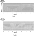
- Fig. 6B illustrates the differential output current I do between the ARCP inverters INV1 and INV2 over one period of the fundamental frequency when a swing time control according to the invention is simulated under the same conditions as in the simulation of Fig. 6A .
- the peak differential output current has been reduced to about 6 A which is only 10% of the original current difference in Fig. 6A .
- FIG.7 An exemplary functional block diagram of a resonant swing time controller logic according to an embodiment of the invention is illustrated in Fig.7 .
- the actual swing time duration is determined or measured by a pre-swing detector 70, a post-swing detector 71, and a timer 72.
- the pre-swing detector 70 and the post-swing detector 71 have inputs receiving the main switch gating signals G 11 and G 21 , or signals representative of them.
- the pre-swing detector 70 and the post-swing detector 71 also takes into account whether a Mode A commutation is happening and also the direction of the commutation from the potential N to the potential P or from the potential P to the potential N.
- the resonant swing time duration is calculated from Mode A commutations only, as only Mode A has a constant swing time which is not affected by load currents.
- the detectors 70 and 72 may be disabled for Mode B commutations.
- the pre-swing detector 70 In Mode A commutation from N to P, the pre-swing detector 70 outputs a pre-swing trigger pulse 70a, when it detects from a change of the gating signal G 21 that the main switch S 21 is turned off at the end of the boosting interval t bA1 , and that the commutation swing of the output voltage U c21 from N to P starts.
- the pre-swing trigger pulse 70a starts a timer 72 to calculate the elapsed time of the resonant swing.
- the post-swing detector 71 outputs a post-swing trigger pulse 71a, when it detects from a change of the gating signal G 11 that the main switch S 11 is turned on at the end of the commutation swing of the output voltage U c21 .
- the post-swing trigger pulse 71a stops the timer 72 which outputs the measured actual resonant swing time t s_meas .
- the pre-swing detector 70 outputs a pre-swing trigger pulse 70a, when it detects from a change of the gating signal G 11 that the main switch S 11 is turned off at the end of the boosting interval t bA1 , and that the commutation swing of the output voltage U c11 from P to N starts.
- the pre-swing trigger pulse 70a starts a timer 72 to calculate the elapsed time of the resonant swing.
- the post-swing detector 71 outputs a post-swing trigger pulse 71a, when it detects from a change of the gating signal G 21 that the main switch S 21 is turned on at the end of the commutation swing of the output voltage U c11 .
- the post-swing trigger pulse 71a stops the timer 72 which outputs the measured actual resonant swing time t s_meas .
- a comparator 73 compares the actual resonant swing time t s_meas with a swing time reference t s_ref and outputs a swing time error signal t s_error which represents the difference between the actual resonant swing time t s_meas and a swing time reference t s_ref .
- the swing time error signal t s_error is fed into an integral controller (I-controller) 75.
- the I-controller 75 forms an integral of the error signal that is used for forming a delay control command aux_delay_cmd.
- the delay control command aux_delay_cmd is the actual delay used in the turn-on gating of the auxiliary switch S a11 or S a21 .
- the I-controller 75 combines (sums) the integral of the error signal with a nominal midpoint delay (max_diff_delay_aux/2) to form the delay control command aux_delay_cmd.
- the I-controller effectively varies or modifies the turn-on delay of an auxiliary switch around the nominal midpoint delay (max_diff_delay_aux/2) within a maximum delay control range (max_diff_delay_aux).
- the delay control range max_diff_delay_aux is split around the nominal midpoint delay to allow for either increasing or decreasing the auxiliary switch turn-on from the nominal midpoint delay to meet the swing time reference t s_ref , i.e., to drive the swing time error signal t s_error towards zero.
- the turn-on instant of the auxiliary switch is respectively advanced or delayed from the turn-on instant corresponding to the nominal midpoint delay.
- the ARCP inverter has respectively more or less time for the buildup of the boost current, which respectively results in a higher or lower boost current, hence respectively leading to a faster resonant swing with a shorter swing time duration or to a slower resonant swing with a longer swing time duration in the ARCP inverter compared to the resonant swing corresponding to the nominal midpoint delay.
- the delay control command aux_delay_cmd is arranged to control an adjustable delay 76 which delays an input auxiliary gating signal G an (e.g., the gating signal G a11 or G a21 ) and outputs a delayed auxiliary gating signal G an ⁇ .
- the delay control commands provided for mode A commutation by the swing time controller may be stored in the swing time controller or in another storage unit to be used in subsequent mode B commutations.
- the main switch such as the main switch S 11 or the main switch S 21 , is turned off at the end of the actual delayed boost time t b ⁇ , and the turn-off timing of the main switch is not impacted by the varying auxiliary switch delays commanded by the swing time duration controller.
- the auxiliary switch delay merely controls the actual starting point of the boosting, i.e., the effective boost time, within the actual delayed boost time.
- the swing time reference t s_ref may be calculated from the dc-link voltage U dc and the boost current (reference) I bA , e.g., by a swing time reference calculator 74 as illustrated in Fig. 7 .
- the calculation of the swing time reference t s_ref may be performed applying and implemented the equations (1), (2), and (3) above, for example.
- the capacitor voltage U c21 may be replaced by U dc /2 in the equations.
- the dc-link voltage U dc may be known (constant) or measured actual value.
- the target boost current I b is typically set to a constant value, regardless of U dc .
- U dc is not a constant.
- Figure 9 is a plot showing an example of the swing time reference t s_ref as function of U dc for a constant boost current I b .
- the swing time controller may essentially reduce the actual boost current too much for a successful ARCP commutation, and the delay the control range gets consumed in compensating for the U dc variation.
- the swing time reference calculator 7 approximates the swing time reference t s_ref using an actual measured value of the dc-link voltage U dc with some readily available approximation means, such as a lookup table indexed by U dc values, linear interpolation, approximation of transcendental functions, etc.
- the resulting swing time reference will thus "breathe” with varying U dc but stay in synchronism among the parallel ARCP half-bridge legs.
- Fig 10 is a graph that shows how the swing time controller drives the swing time to this reference value after some initial transients at the start of the simulation.
- the switching control and swing time control techniques described herein may be implemented by various means. For example, these techniques may be implemented in hardware (one or more devices), firmware (one or more devices), software (one or more modules), or combinations thereof. For a firmware or software, implementation can be through modules (e.g., procedures, functions, and so on) that perform the functions described herein.
- the software codes may be stored in any suitable, processor/computer-readable data storage medium(s) or memory unit(s) and executed by one or more processors/computers.
- the data storage medium or the memory unit may be implemented within the processor/computer or external to the processor/computer, in which case it can be communicatively coupled to the processor/computer via various means as is known in the art.
- components of systems described herein may be rearranged and/or complimented by additional components in order to facilitate achieving the various aspects, goals, advantages, etc., described with regard thereto, and are not limited to the precise configurations set forth in a given figure, as will be appreciated by one skilled in the art.
Landscapes
- Engineering & Computer Science (AREA)
- Power Engineering (AREA)
- Inverter Devices (AREA)
Priority Applications (3)
| Application Number | Priority Date | Filing Date | Title |
|---|---|---|---|
| EP23180651.4A EP4482004A1 (de) | 2023-06-21 | 2023-06-21 | Stromrichtersystem |
| CN202410521861.8A CN119182269A (zh) | 2023-06-21 | 2024-04-28 | 功率转换器系统 |
| US18/741,109 US20240429832A1 (en) | 2023-06-21 | 2024-06-12 | Power converter system |
Applications Claiming Priority (1)
| Application Number | Priority Date | Filing Date | Title |
|---|---|---|---|
| EP23180651.4A EP4482004A1 (de) | 2023-06-21 | 2023-06-21 | Stromrichtersystem |
Publications (1)
| Publication Number | Publication Date |
|---|---|
| EP4482004A1 true EP4482004A1 (de) | 2024-12-25 |
Family
ID=86942522
Family Applications (1)
| Application Number | Title | Priority Date | Filing Date |
|---|---|---|---|
| EP23180651.4A Pending EP4482004A1 (de) | 2023-06-21 | 2023-06-21 | Stromrichtersystem |
Country Status (3)
| Country | Link |
|---|---|
| US (1) | US20240429832A1 (de) |
| EP (1) | EP4482004A1 (de) |
| CN (1) | CN119182269A (de) |
Citations (5)
| Publication number | Priority date | Publication date | Assignee | Title |
|---|---|---|---|---|
| US5047913A (en) | 1990-09-17 | 1991-09-10 | General Electric Company | Method for controlling a power converter using an auxiliary resonant commutation circuit |
| EP0524398A2 (de) | 1991-07-23 | 1993-01-27 | Kabushiki Kaisha Meidensha | Schaltkreis zur Kontrolle des Ausgangsstroms von parallel geschalteten pulsbreitenmodulierten Wechslerichtern |
| US7068525B2 (en) | 2002-12-06 | 2006-06-27 | Loher Gmbh | Method of operating multiple parallel-connected pulse-controlled inverters |
| US8432714B2 (en) | 2009-01-27 | 2013-04-30 | Abb Oy | Load balancing of parallel connected inverter modules |
| WO2017079125A1 (en) | 2015-11-02 | 2017-05-11 | Servicenow, Inc. | Universal automatic data update detection and publication |
Family Cites Families (2)
| Publication number | Priority date | Publication date | Assignee | Title |
|---|---|---|---|---|
| US8385085B2 (en) * | 2007-09-25 | 2013-02-26 | Daihen Corporation | PWM signal generator, and inverter equipped with this PWM signal generator |
| US10666127B2 (en) * | 2017-08-14 | 2020-05-26 | Ge Global Sourcing Llc | Power system and method |
-
2023
- 2023-06-21 EP EP23180651.4A patent/EP4482004A1/de active Pending
-
2024
- 2024-04-28 CN CN202410521861.8A patent/CN119182269A/zh active Pending
- 2024-06-12 US US18/741,109 patent/US20240429832A1/en active Pending
Patent Citations (5)
| Publication number | Priority date | Publication date | Assignee | Title |
|---|---|---|---|---|
| US5047913A (en) | 1990-09-17 | 1991-09-10 | General Electric Company | Method for controlling a power converter using an auxiliary resonant commutation circuit |
| EP0524398A2 (de) | 1991-07-23 | 1993-01-27 | Kabushiki Kaisha Meidensha | Schaltkreis zur Kontrolle des Ausgangsstroms von parallel geschalteten pulsbreitenmodulierten Wechslerichtern |
| US7068525B2 (en) | 2002-12-06 | 2006-06-27 | Loher Gmbh | Method of operating multiple parallel-connected pulse-controlled inverters |
| US8432714B2 (en) | 2009-01-27 | 2013-04-30 | Abb Oy | Load balancing of parallel connected inverter modules |
| WO2017079125A1 (en) | 2015-11-02 | 2017-05-11 | Servicenow, Inc. | Universal automatic data update detection and publication |
Non-Patent Citations (5)
| Title |
|---|
| "The auxiliary resonant commutated pole converter", IEEE-IAS CONFERENCE PROCEEDINGS, 1990, pages 1228 - 35 |
| PROTIWA F-F ET AL: "A 20 KVA AUXILIARY RESONANT COMMUTATED POLE CONVERTER. ÖDESIGN AND PRACTICAL EXPERIENCES", EPE '95: 6TH. EUROPEAN CONFERENCE ON POWER ELECTRONICS AND APPLICATIONS. SEVILLA, SEPT. 19 - 21, 1995; [EUROPEAN CONFERENCE ON POWER ELECTRONICS AND APPLICATIONS], BRUSSELS, EPE ASSOCIATION, B, vol. 2, 19 September 1995 (1995-09-19), pages 2.111 - 2.116, XP000537731 * |
| TABRIZI GHOLAMREZA ET AL: "Influence of DC Supply Voltage Unbalances on the Performance of ARCP Inverters", 2022 24TH EUROPEAN CONFERENCE ON POWER ELECTRONICS AND APPLICATIONS (EPE'22 ECCE EUROPE), EPE ASSOCIATION, 5 September 2022 (2022-09-05), pages 1 - 9, XP034207761 * |
| TABRIZI GHOLAMREZA ET AL: "Optimized Design Method and Control of an Auxiliary Resonant Commutated Pole Inverter for Two Level Photovoltaic Inverters", 3 May 2021 (2021-05-03), pages 1662 - 1669, XP093103787, Retrieved from the Internet <URL:https://ieeexplore.ieee.org/stampPDF/getPDF.jsp?tp=&arnumber=9472446&ref=aHR0cHM6Ly9pZWVleHBsb3JlLmllZWUub3JnL2RvY3VtZW50Lzk0NzI0NDY=> [retrieved on 20231121] * |
| ZOCHER MARKUS ET AL: "Auxiliary Resonant Commutated Pole Inverter (ARCPI) Operation Using online voltage measurements", 2022 IEEE APPLIED POWER ELECTRONICS CONFERENCE AND EXPOSITION (APEC), IEEE, 20 March 2022 (2022-03-20), pages 1592 - 1597, XP034125179, DOI: 10.1109/APEC43599.2022.9773560 * |
Also Published As
| Publication number | Publication date |
|---|---|
| CN119182269A (zh) | 2024-12-24 |
| US20240429832A1 (en) | 2024-12-26 |
Similar Documents
| Publication | Publication Date | Title |
|---|---|---|
| US5047913A (en) | Method for controlling a power converter using an auxiliary resonant commutation circuit | |
| US6603675B1 (en) | Apparatus and a method for voltage conversion | |
| US7577007B2 (en) | Power converting apparatus | |
| US8830711B2 (en) | Hybrid switch for resonant power converters | |
| US10608522B2 (en) | Electrical circuit with auxiliary voltage source for zero-voltage switching in DC-DC converter under all load conditions | |
| Norrga | Experimental study of a soft-switched isolated bidirectional AC–DC converter without auxiliary circuit | |
| US20100246231A1 (en) | Achieving zvs in a two quadrant converter using a simplified auxiliary circuit | |
| JP6706811B2 (ja) | スナバ回路及びそれを用いた電力変換システム | |
| Kim et al. | New bilateral zero voltage switching AC/AC converter using high frequency partial-resonant link | |
| US20240429833A1 (en) | Arrangement for Current Sharing of Parallel-Connected Converters | |
| US10050556B2 (en) | Voltage source converter and control thereof | |
| US20240348180A1 (en) | Arcp converter and control thereof | |
| US10848071B2 (en) | Highly reliable and compact universal power converter | |
| US20240178739A1 (en) | Control apparatus for an arcp inverter | |
| Pal et al. | A PWM ZVS high-frequency-link three-phase inverter with T-type NPC unfolder | |
| Tripathi et al. | MVDC microgrids enabled by 15kV SiC IGBT based flexible three phase dual active bridge isolated DC-DC converter | |
| Ishikawa et al. | A novel soft-switched PWM current source inverter with voltage clamped circuit | |
| Kopacz et al. | High-frequency SiC-based medium voltage quasi-2-level flying capacitor DC/DC converter with zero voltage switching | |
| EP4482004A1 (de) | Stromrichtersystem | |
| US20240305216A1 (en) | Arrangement For Current Sharing Of Parallel-Connected Inverters | |
| EP4482003A1 (de) | Anordnung zur stromteilung von parallel geschalteten wandlern | |
| EP3571757B1 (de) | Energierückstellung eines modularen mehrpegelumsetzers | |
| US6061256A (en) | Apparatus for conversion of a three-phase voltage into an isolated DC voltage | |
| EP1487094A1 (de) | Wandler und Verfharen zu deren Regelung | |
| Ram et al. | An si+ sic based hybrid voltage source inverter topology for transformerless grid tied inverters |
Legal Events
| Date | Code | Title | Description |
|---|---|---|---|
| PUAI | Public reference made under article 153(3) epc to a published international application that has entered the european phase |
Free format text: ORIGINAL CODE: 0009012 |
|
| STAA | Information on the status of an ep patent application or granted ep patent |
Free format text: STATUS: THE APPLICATION HAS BEEN PUBLISHED |
|
| AK | Designated contracting states |
Kind code of ref document: A1 Designated state(s): AL AT BE BG CH CY CZ DE DK EE ES FI FR GB GR HR HU IE IS IT LI LT LU LV MC ME MK MT NL NO PL PT RO RS SE SI SK SM TR |
|
| STAA | Information on the status of an ep patent application or granted ep patent |
Free format text: STATUS: REQUEST FOR EXAMINATION WAS MADE |
|
| 17P | Request for examination filed |
Effective date: 20250613 |
|
| STAA | Information on the status of an ep patent application or granted ep patent |
Free format text: STATUS: EXAMINATION IS IN PROGRESS |