EP4481812A1 - Radio frequency semiconductor device and method for fabricating a radio frequency semiconductor device - Google Patents
Radio frequency semiconductor device and method for fabricating a radio frequency semiconductor device Download PDFInfo
- Publication number
- EP4481812A1 EP4481812A1 EP23180220.8A EP23180220A EP4481812A1 EP 4481812 A1 EP4481812 A1 EP 4481812A1 EP 23180220 A EP23180220 A EP 23180220A EP 4481812 A1 EP4481812 A1 EP 4481812A1
- Authority
- EP
- European Patent Office
- Prior art keywords
- semiconductor device
- metal layer
- semiconductor chip
- semiconductor
- chip
- Prior art date
- Legal status (The legal status is an assumption and is not a legal conclusion. Google has not performed a legal analysis and makes no representation as to the accuracy of the status listed.)
- Withdrawn
Links
Images

Classifications
-
- H—ELECTRICITY
- H10—SEMICONDUCTOR DEVICES; ELECTRIC SOLID-STATE DEVICES NOT OTHERWISE PROVIDED FOR
- H10W—GENERIC PACKAGES, INTERCONNECTIONS, CONNECTORS OR OTHER CONSTRUCTIONAL DETAILS OF DEVICES COVERED BY CLASS H10
- H10W42/00—Arrangements for protection of devices
- H10W42/20—Arrangements for protection of devices protecting against electromagnetic or particle radiation, e.g. light, X-rays, gamma-rays or electrons
-
- H—ELECTRICITY
- H10—SEMICONDUCTOR DEVICES; ELECTRIC SOLID-STATE DEVICES NOT OTHERWISE PROVIDED FOR
- H10W—GENERIC PACKAGES, INTERCONNECTIONS, CONNECTORS OR OTHER CONSTRUCTIONAL DETAILS OF DEVICES COVERED BY CLASS H10
- H10W40/00—Arrangements for thermal protection or thermal control
- H10W40/20—Arrangements for cooling
- H10W40/22—Arrangements for cooling characterised by their shape, e.g. having conical or cylindrical projections
-
- H—ELECTRICITY
- H10—SEMICONDUCTOR DEVICES; ELECTRIC SOLID-STATE DEVICES NOT OTHERWISE PROVIDED FOR
- H10W—GENERIC PACKAGES, INTERCONNECTIONS, CONNECTORS OR OTHER CONSTRUCTIONAL DETAILS OF DEVICES COVERED BY CLASS H10
- H10W42/00—Arrangements for protection of devices
- H10W42/20—Arrangements for protection of devices protecting against electromagnetic or particle radiation, e.g. light, X-rays, gamma-rays or electrons
- H10W42/261—Arrangements for protection of devices protecting against electromagnetic or particle radiation, e.g. light, X-rays, gamma-rays or electrons characterised by their shapes or dispositions
- H10W42/276—Arrangements for protection of devices protecting against electromagnetic or particle radiation, e.g. light, X-rays, gamma-rays or electrons characterised by their shapes or dispositions the arrangements being on an external surface of the package, e.g. on the outer surface of an encapsulation
-
- H—ELECTRICITY
- H10—SEMICONDUCTOR DEVICES; ELECTRIC SOLID-STATE DEVICES NOT OTHERWISE PROVIDED FOR
- H10W—GENERIC PACKAGES, INTERCONNECTIONS, CONNECTORS OR OTHER CONSTRUCTIONAL DETAILS OF DEVICES COVERED BY CLASS H10
- H10W44/00—Electrical arrangements for controlling or matching impedance
- H10W44/20—Electrical arrangements for controlling or matching impedance at high-frequency [HF] or radio frequency [RF]
-
- H—ELECTRICITY
- H10—SEMICONDUCTOR DEVICES; ELECTRIC SOLID-STATE DEVICES NOT OTHERWISE PROVIDED FOR
- H10W—GENERIC PACKAGES, INTERCONNECTIONS, CONNECTORS OR OTHER CONSTRUCTIONAL DETAILS OF DEVICES COVERED BY CLASS H10
- H10W74/00—Encapsulations, e.g. protective coatings
- H10W74/10—Encapsulations, e.g. protective coatings characterised by their shape or disposition
- H10W74/111—Encapsulations, e.g. protective coatings characterised by their shape or disposition the semiconductor body being completely enclosed
- H10W74/114—Encapsulations, e.g. protective coatings characterised by their shape or disposition the semiconductor body being completely enclosed by a substrate and the encapsulations
- H10W74/117—Encapsulations, e.g. protective coatings characterised by their shape or disposition the semiconductor body being completely enclosed by a substrate and the encapsulations the substrate having spherical bumps for external connection
-
- H—ELECTRICITY
- H10—SEMICONDUCTOR DEVICES; ELECTRIC SOLID-STATE DEVICES NOT OTHERWISE PROVIDED FOR
- H10W—GENERIC PACKAGES, INTERCONNECTIONS, CONNECTORS OR OTHER CONSTRUCTIONAL DETAILS OF DEVICES COVERED BY CLASS H10
- H10W74/00—Encapsulations, e.g. protective coatings
- H10W74/10—Encapsulations, e.g. protective coatings characterised by their shape or disposition
- H10W74/111—Encapsulations, e.g. protective coatings characterised by their shape or disposition the semiconductor body being completely enclosed
- H10W74/121—Encapsulations, e.g. protective coatings characterised by their shape or disposition the semiconductor body being completely enclosed by multiple encapsulations, e.g. by a thin protective coating and a thick encapsulation
-
- H—ELECTRICITY
- H10—SEMICONDUCTOR DEVICES; ELECTRIC SOLID-STATE DEVICES NOT OTHERWISE PROVIDED FOR
- H10W—GENERIC PACKAGES, INTERCONNECTIONS, CONNECTORS OR OTHER CONSTRUCTIONAL DETAILS OF DEVICES COVERED BY CLASS H10
- H10W99/00—Subject matter not provided for in other groups of this subclass
-
- H—ELECTRICITY
- H01—ELECTRIC ELEMENTS
- H01Q—ANTENNAS, i.e. RADIO AERIALS
- H01Q1/00—Details of, or arrangements associated with, antennas
- H01Q1/12—Supports; Mounting means
- H01Q1/22—Supports; Mounting means by structural association with other equipment or articles
- H01Q1/2283—Supports; Mounting means by structural association with other equipment or articles mounted in or on the surface of a semiconductor substrate as a chip-type antenna or integrated with other components into an IC package
-
- H—ELECTRICITY
- H10—SEMICONDUCTOR DEVICES; ELECTRIC SOLID-STATE DEVICES NOT OTHERWISE PROVIDED FOR
- H10W—GENERIC PACKAGES, INTERCONNECTIONS, CONNECTORS OR OTHER CONSTRUCTIONAL DETAILS OF DEVICES COVERED BY CLASS H10
- H10W44/00—Electrical arrangements for controlling or matching impedance
- H10W44/20—Electrical arrangements for controlling or matching impedance at high-frequency [HF] or radio frequency [RF]
- H10W44/241—Electrical arrangements for controlling or matching impedance at high-frequency [HF] or radio frequency [RF] for passive devices or passive elements
- H10W44/248—Electrical arrangements for controlling or matching impedance at high-frequency [HF] or radio frequency [RF] for passive devices or passive elements for antennas
Definitions
- the present disclosure relates to a radio frequency semiconductor device and in particular to a radio frequency semiconductor device with a metal layer. In addition, the present disclosure relates to method of manufacturing such devices.
- RF semiconductor devices play a crucial role.
- EMI electromagnetic interference
- the first surface and second surface extend along a lateral direction and the sidewalls extend along a vertical direction.
- a metal layer is provided external to the active chip region, wherein the metal layer faces the second surface of the semiconductor chip, wherein the metal layer has a thickness that is below a skin depth corresponding to the operating frequency range.
- a method for a radio frequency (RF) semiconductor device to process RF signals in an operating frequency range comprises:
- FIG. 1 shows a cross sectional view of a radio frequency (RF) semiconductor device 100.
- the RF semiconductor device 100 has a semiconductor chip 102 configured to operate in a predetermined frequency range such as a millimeter-wave frequency range, for example in a first frequency range from 1 GHz to 500 GHz or in a second frequency range from 60 GHz to 90 GHz.
- the semiconductor chip 102 may correspond to a radar chip and may be used as a transmitter, a receiver, a sensor, a detector etc.
- the semiconductor chip may be a 5G or 6G communication chip, a high data transfer communication system, wireless backhaul systems of body scanning systems for security.
- the RF signal or RF signals refer to the RF signal or RF signals in the operating frequency range.
- the semiconductor chip 102 has a first surface 104, a second surface 106 opposite to the first surface 104 and sidewalls 108.
- the first surface 104 and the second surface 106 may be referred to as a first main surface and a second main surface.
- the first surface 104 and second surface 106 extend along a lateral direction and the sidewalls 108 extend along a vertical direction.
- An active chip area having transistors and other circuit elements is provided in the semiconductor chip 102.
- the active chip area may be capable of generating and analyzing RF signals and other signals. In some examples, the active chip area may also be referred as an RF chip circuitry.
- the first surface 104 of the semiconductor chip 102 is arranged on a first side 112 of a redistribution layer 110 and an electrical contact is established between the semiconductor chip 102 and electrically conductive structures of the redistribution layer 110.
- the electrical contact may be formed by a bond pad which may be made of aluminum and/or copper. This allows the RF signals to be transmitted from the semiconductor chip 102 to the electrical contacts and/or vice-versa.
- the RF semiconductor device 100 may correspond to a wafer level package.
- the semiconductor chip 102 may have a thickness selected from a range of 100 ⁇ m to 1000 ⁇ m, wherein the thickness is measured between the first surface 104 and the second surface 106 of the semiconductor chip 102. In some examples the semiconductor chip 102 may have the thickness selected in a range of 50 ⁇ m to 400 ⁇ m. In some examples, the thickness of the semiconductor chip 102 can also be measured between the first side 112 of the redistribution layer 110 and the second surface 106 of the semiconductor chip 102.
- the redistribution layer 110 may have one or more electrically conductive structures in form of metal lines or metal planes, running parallel to the first surface 104 of the semiconductor chip 102.
- the electrically conductive structures route the electric current in the RF semiconductor device 100 and are electrically isolated from each other by a dielectric material.
- the conductive structures may be made of aluminum, copper or a copper alloy.
- the dielectric material may comprise an oxide or a nitride.
- the redistribution layer 110 has a second side 120 opposite to the first side 112.
- a plurality of first solder balls 122 is arranged on the second side 120 of the redistribution layer 110. Accordingly, the redistribution layer 110 establishes the electrical connection between the plurality of first solder balls 122 and the semiconductor chip 102.
- a printed circuit board (PCB) which is not shown in Figure 1 may be electrically and mechanically mounted to the plurality of first solder balls 122.
- the plurality of first solder balls 122 may comprise at least one of Sn, Ag, or Cu.
- Each solder ball of the plurality of first solder balls 122 may have diameter in a range between 200 ⁇ m and 400 ⁇ m and pitches in a range between of 400 ⁇ m and 600 ⁇ m.
- Flip-Chip BGAs (Ball Grid Arrays) or Wirebond-BGA may be used for establishing the electrical and mechanical connection to the PCB.
- a metal layer 114 is disposed over the semiconductor chip 102 external to the active chip area.
- the metal layer 114 has a top surface 114a and a bottom surface 114b opposite to each other.
- the bottom surface 114b of the metal layer 114 faces the second surface 106 of the semiconductor chip 102.
- the metal layer 114 may have smooth or rough top surface 114a and bottom surface 114b, however a thickness of the metal layer 114 is always below than a skin depth of the metal layer 114 in the corresponding operating frequency range, wherein the thickness of the metal layer 114 is measured between the top 114a and bottom surface 114b in the vertical direction. In some examples, the thickness is selected such that the thickness of the metal layer 114 is along the extension of the metal layer 114 always below the skin depth.
- the metal layer 114 may absorb the RF signals from the RF chip circuitry and thereby reduces the interference among the RF chip circuitry components, for example from one channel to another channel. In other words, the metal layer 114 reduces the RF signals reflecting back to the RF chip circuitry and hence improves the RF properties e.g., channel to channel isolation of the RF semiconductor device 100. The metal layer 114 may also absorb the RF signals originating from external elements and provides RF shielding to the RF semiconductor device 100 from the external elements.
- the optimum performance of the RF semiconductor device 100 can be achieved by choosing the relevant thickness for the metal layer 114 depending upon the operating frequency of the RF semiconductor device 100 to be below the skin depth.
- the improvement of the absorption properties of a metal layer is based on the skin depth effect, wherein the skin depth refers to how deeply the RF signal can penetrate the metal layer.
- the skin depth refers to how deeply the RF signal can penetrate the metal layer.
- the skin depth depends on the frequency of the RF signal as well as the properties of the metal layer.
- the metal layer 114 comprises a metal or a metal alloy e.g. Au, Al, Cu Ti, Ta, Ti, Ru, TaN, TiN, Co 90 Fe 10 , Ni 80 Fe 20 , Ni 60 Cr 40 but not limited to the aforementioned examples.
- the conductivity s of the metal layer depends on its thickness.
- the metal layer may have a thickness between 1nm and 150nm for maximum absorption in the first frequency range from 1 GHz to 500GHz. For ruthenium as an example, a thickness between 2.5nm and 10nm might be chosen to maximize the absorption for the second frequency range from 60GHz to 90GHz.
- the metal layer 114 With the introduction of the metal layer 114 on the semiconductor chip 102 a new concept is introduced which allows an efficient, cost effective and configurable absorption concept of RF signals for RF semiconductor devices.
- the metal layer 114 can be deposited over the semiconductor device 102 using technology for e.g., sputter deposition or vapor deposition (PVD), evaporation, electrochemical deposition (ECD), Electroless deposition (ED), ALD, Metal film lamination.
- PVD sputter deposition or vapor deposition
- ECD electrochemical deposition
- ED Electroless deposition
- ALD Metal film lamination.
- the new concept is inexpensive and highly flexible since an adaption of the absorption properties can be achieved by varying the thickness of the metal layer 114 for the requirement of various RF semiconductor devices.
- the thickness changes required for adaption of the absorption properties are within a nanometer or micrometer range which practically does not affect the device dimension which is in the millimeter range nor requires any additional steps or material.
- the concept can be used for single-chip RF devices or multi-chip RF devices in which multiple semiconductor chips are arranged above or lateral to each other within a semiconductor device.
- the metal layer 114 can extend completely over an area of the second main surface of the semiconductor chip 102 or at least a majority of the second main surface of the semiconductor chip 102.
- the metal layer 114 may in other examples be arranged to extend only over specific semiconductor chip areas of particular interest.
- the new concept introduced in this application is further well-suited for fan-out packages where the RF signals are in a fan-out area significantly influenced by interference from other RF signals and will be described with respect to examples later in the description.
- the metal layer 114 may extend in the complete fan-out area or in a majority of the fan-out area or in a portion of the fan-out area.
- the thickness of the semiconductor chip 102 may be in a range of a quarter wavelength of the RF signal. This configuration provides an additional advantage that the RF signals which are reflected at the second surface 106 will have 180° phase shift with respect to the RF signals originating at the RF chip circuitry and/or the first surface 104 and hence will vanish from destructive interference within the semiconductor chip 102 and thereby further reducing the interference among the RF chip circuitry components.
- At least one antenna may be configured on the second surface 106 of the semiconductor chip 102 such that the at least one antenna is exposed and separated by a gap from the metal layer 114. Additionally, the metal layer 114 may reduce the interference between the at least one antenna.
- FIG 2 shows an example of an RF semiconductor device 200 which may include some or all features of the RF semiconductor device 100 of Figure 1 .
- the metal layer 114 is a first metal layer of a plurality of metal layers 216 (e.g. a stack of metal layers 216), wherein each metal layer of the plurality of metal layers 216 comprises a top surface 216a and a bottom surface 216b opposite to their respective top surface 216a.
- the plurality of metal layers 216 is arranged between the first surface 104 and second surface 106 of the semiconductor chip 102, wherein the bottom surface 216b of each metal layer of the plurality of metal layers 216 faces the second surface 106.
- Each metal layer of the plurality of metal layer 216 has a thickness that is below a skin depth corresponding to the operating frequency range of the semiconductor device 200, wherein the thickness of each metal layer of the plurality of metal layers 216 is measured between their respective top surfaces 216a and bottom surfaces 216b. Accordingly, each of the plurality of metal layers 216 provides the same properties and characteristics as outlined above for the metal layer 114 in order to improve the RF properties and reduce EMI.
- a material between the respective metal layers of the plurality of metal layers 216 may be a non-metallic material or a dielectric material, e.g. mold compound, silicon or silicon dioxide.
- Each metal layer of the plurality of metal layers 216 may be separated by a distance in the range of quarter wavelength of the operating frequency range or a distance other than the quarter wavelength of the operating frequency range.
- the quarter wavelength separation among the plurality of metal layers 216 further improves the RF characteristics in that the RF signals reflected at each metal layer of the plurality of metal layers 216 will have 180° phase shift with respect to the RF signals reflected at the adjacent metal layer of the plurality of metal layer 216 and hence the RF signals will vanish due to destructive interference.
- the RF semiconductor device 200 combines the absorption, transmission and reflection properties of the plurality of metal layer 216.
- each metal layer in the plurality of metal layers 216 may comprise of a same metal or different metals.
- RF signals of various frequencies may be absorbed.
- the RF semiconductor device 300 comprises a mold compound 302.
- the mold compound 302 covers completely or at least a portion of the second surface 106 and completely or at least a portion of the sidewalls 108 of the semiconductor chip 102 and a first portion of the first side 112 of the redistribution layer 110 that is not covered by the semiconductor chip 102.
- the mold compound 302 comprises an outer surface of the RF semiconductor device wherein the outer surface has a top side 304 and sidewalls 308.
- the top side 304 faces and extends beyond the second surface 106 of the semiconductor chip 102 and the fan-out area and the sidewalls 308 of the RF semiconductor device face the sidewalls 108 of the semiconductor chip 102.
- the thickness of at least the first region of the mold compound 302, measured in the fan-out-area may be in the range of a quarter-wavelength of the operating frequency of the RF semiconductor device 300.
- the RF signals which are reflected at the top side 304 will have 180° phase shift with respect to the RF signals reflected from the second surface 106 of the semiconductor chip 102 or from the first side 112 of the redistribution layer 110 and hence the RF signals will vanish from destructive interference within the RF semiconductor device 300.
- the mold compound 302 may be epoxy, filled epoxy, glass fiber filled epoxy, thermoset polymers, thermoplastic polymers, or elastomer polymers but not limited to the aforementioned examples.
- Figure 4 shows an example of an RF semiconductor device 400 which may include some or all features of the RF semiconductor device 200 of Figure 2 and the RF semiconductor device 300 of Figure 3 .
- the first metal layer 314 is a metal layer of a plurality of metal layers 416, and the plurality of metal layers 416 has the same characteristics and functionalities and thicknesses as the plurality of metal layers 216 of the Figure 2 .
- the plurality of metal layers 416 may be separated by a quarter wavelength of the operating frequency, as outlined above with respect to the plurality of metal layer 216.
- Figure 5 shows an example of an RF semiconductor device 500 which may include some or all features of the RF semiconductor device 300 of Figure 3 .
- the RF semiconductor device 500 comprises a second metal layer 514 similar to the metal layer 114 described above which is disposed over the second surface 106 of the semiconductor chip 102.
- the second metal layer 514 has the same functionalities and characteristics of the metal layer 114 of Figure 1 .
- the first metal layer 314 on the top side 304 of the RF semiconductor device 500 absorbs the RF signals in the mold compound 302 and in the fan-out area, whereas the second metal layer 514 on the second surface 106 of the semiconductor chip 102 absorbs the RF signals within the semiconductor chip 102.
- the RF signals propagating in the RF semiconductor device 500 may scatter between the first metal layer 314 and the second metal layer 514 and eventually vanish.
- Figure 7 shows an example of an RF semiconductor device 700 which may include some or all feature of the RF semiconductor device 600 of Figure 6 .
- a second plurality of metal layers 716 is provided in Figure 7 which includes the second metal layer 514.
- the second plurality of metal layers 716 is arranged between the first surface 104 and the second surface 106 of the semiconductor chip 102.
- the second plurality of metal layers 716 has the same functionalities and characteristics of the plurality of metal layers 216 of Figure 2 .
- Figure 8 shows an example of an RF semiconductor device 800 which may include some or all features of the RF semiconductor device 300 of Figure 3 .
- the first metal layer 314 is shown to include at least one recess 802.
- the at least one recess 802 may be a groove, a trench, a cut etc.
- the at least one recess 802 may be configured to accommodate an antenna 804 arranged on the top side 304 of the RF semiconductor device 800.
- the at least one antenna 804 may be configured to have a same horizontal level as of the bottom surface 314b of the first metal layer 314.
- the at least one antenna 804 is separated from the first metal layer 314 by a gap between the first metal layer 314 and the at least one antenna 804 in the lateral direction.
- the first metal layer 314 may absorb the RF signals and hence the interference originating from the at least one antenna 804 or between multiple of the at least one antenna can be reduced and tuned.
- Figure 8A shows an example of an RF semiconductor device 800A which may include some or all features of the RF semiconductor device 800 of Figure 8 .
- the RF semiconductor device 800A differs from the RF semiconductor device 800 regarding the position of the first metal layer 314 and the position of the at least one antenna 804.
- the first metal layer 314 and the at least one antenna 804 are arranged on the second side 120 of the redistribution layer 110.
- the first metal layer 314 is arranged in the fan-out area in the vicinity of the at least one antenna 804, wherein the first metal layer 314 may absorb the RF signal and reduce the interference originating from the at least one antenna 804 in the fan-out area.
- a heat sink can be mounted on the top side 304 of the RF semiconductor device 800.
- a thermal interface material can be arranged between the top side 304 of the RF semiconductor device and the heat sink.
- the thermal interface material may comprise for e.g., Gap Filler Pads, Dispensable Gap Fillers, Phase Change and having thermal conductivity in a range of 1 to 20 W/mK.
- FIG 10 shows an example of an RF semiconductor device 1000 which may include some or all features of the RF semiconductor device 100 of Figure 1 .
- the RF semiconductor device 1000 comprises a plurality of second solder balls 1002, wherein the plurality of second solder balls 1002 faces the plurality of first solder balls 122. In the lateral direction, the plurality of second solder balls 1002 extends beyond the plurality of first solder balls 122.
- the plurality of second solder balls 1002 may comprise the same material and may have the same or different diameters and pitches as the plurality of first solder balls 122.
- a substrate 1004 is sandwiched between the plurality of first 122 and second solder balls 1002.
- the substrate 1004 may comprise of laminate or FR4 or Bismaleimide Triazine material, wherein the substrate 1004 may comprise a vertical or horizontal interconnects.
- the RF semiconductor device 1000 further comprises a lid 1006, wherein the lid 1006 is a hollow structure having a main surface 1006a and side legs 1006b.
- the side legs 1006b are perpendicular to the main surface 1006a.
- the lid 1006 is mounted on the semiconductor chip 102 such that the main surface 1006a faces and extends beyond the second surface 106 having the metal layer 114.
- the side legs 1006b are mounted on the substrate 1004 and face the sidewalls 108 of the semiconductor chip 102.
- the side legs 1006b can be mounted to the substrate using an adhesive.
- a layer of thermal interface material 1010 is arranged between the metal layer 114 and a part of the main surface 1006a of the lid 1006 to provide mechanical and thermal stability between the semiconductor chip 102 and the lid 1006.
- the lid 1006 may comprise of a metal or a non-metal material and provides electrical shielding, thermal heat distribution and thermo-mechanical stability in the RF semiconductor device 1000.
- the metal and non-metal material may comprise
Landscapes
- Semiconductor Integrated Circuits (AREA)
- Physics & Mathematics (AREA)
- Health & Medical Sciences (AREA)
- Electromagnetism (AREA)
- Toxicology (AREA)
- Junction Field-Effect Transistors (AREA)
Abstract
According to an example of the invention, a radio frequency (RF) semiconductor device to process RF signals in an operating frequency range comprising a semiconductor chip comprising a first surface, a second surface, sidewalls and an active chip region. The first surface and second surface extend along a lateral direction and the sidewalls extend along a vertical direction.
Description
- The present disclosure relates to a radio frequency semiconductor device and in particular to a radio frequency semiconductor device with a metal layer. In addition, the present disclosure relates to method of manufacturing such devices.
- In the area of advanced driver assistant systems (ADAS), RF semiconductor devices play a crucial role. To improve the performance and functionality of the RF semiconductor devices, more and more functionalities are packed into components with small packages leading to an electromagnetic interference (EMI) coupling between the electrical circuits and other components of the RF semiconductor devices. As RF semiconductor devices are becoming smaller and tightly packed, they are also more vulnerable to the EMI.
- Accordingly, it is an object of this application to provide a concept for an RF semiconductor device which reduces the electromagnetic interference in the RF semiconductor device. This object is solved by an RF semiconductor device according to claim 1 and a method of fabricating a radio frequency semiconductor device according to claim 19.
- According to an example of the invention, a radio frequency (RF) semiconductor device to process RF signals in an operating frequency range comprises a semiconductor chip comprising a first surface, a second surface, sidewalls and an active chip region. The first surface and second surface extend along a lateral direction and the sidewalls extend along a vertical direction. A metal layer is provided external to the active chip region, wherein the metal layer faces the second surface of the semiconductor chip, wherein the metal layer has a thickness that is below a skin depth corresponding to the operating frequency range.
- According to an example of the invention a method for a radio frequency (RF) semiconductor device to process RF signals in an operating frequency range comprises:
- providing a semiconductor chip comprising a first surface, a second surface, sidewalls and an active chip region, the first surface and second surface extending along a lateral direction and the sidewalls extending along a vertical direction,
- providing a metal layer external to the active chip region, wherein the metal layer faces the second surface of the semiconductor chip, wherein the metal layer has a thickness that is below a skin depth corresponding to the operating frequency range.
- Those skilled in the art will recognize additional features and advantages upon reading the following detailed description, and upon viewing the accompanying drawings.
- The present disclosure is illustrated by way of example, and not by way of limitation, in the figures of the accompanying drawings in which like reference numerals refer to similar or identical elements. The elements of the drawings are not necessarily to scale relative to each other. The features of the various illustrated examples can be combined unless they exclude each other.
-
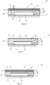
Fig. 1 illustrates a cross-sectional view of an RF semiconductor device. -
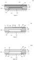
Fig. 2 illustrates a cross-sectional view of an RF semiconductor device. -
Fig. 3 illustrates a cross-sectional view of an RF semiconductor device. -
Fig. 4 illustrates a cross-sectional view of an RF semiconductor device. -
Fig. 5 illustrates a cross-sectional view of an RF semiconductor device. -
Fig. 6 illustrates a cross-sectional view of an RF semiconductor device. -
Fig. 7 illustrates a cross-sectional view of an RF semiconductor device. -
Fig. 8 illustrates a cross-sectional view of an RF semiconductor device. -
Fig. 8A illustrates a cross-sectional view of an RF semiconductor device. -
Fig. 9 illustrates a cross-sectional view of an RF semiconductor device. -
Fig. 10 illustrates a cross-sectional view of an RF semiconductor device. -
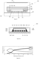
Fig. 11 illustrates an experimental measurement of reflection, transmission, and absorption of a metal layer. - In the following description, directional terminology, such as "top", "bottom", "upper", "lower" "front", "back" etc., is used with reference to the orientation of figures being described. The components of the disclosure can be positioned in a number of different orientations, the directional terminology is used for purposes of illustration and is in no way limiting.
- Furthermore, to the extent that the terms "include", "have", "with" or other variants thereof are used in either the detailed description or the claims, such terms are intended to be inclusive in a manner similar to the term "comprise". The terms "coupled" and "connected", along with derivatives thereof may be used. It should be understood that these terms may be used to indicate that two elements co-operate or interact with each other regardless of whether they are in direct physical or electrical contact, or they are not in direct contact with each other; intervening elements or layers may be provided between the "bonded", "attached", or "connected" elements.
-
Figure 1 shows a cross sectional view of a radio frequency (RF)semiconductor device 100. TheRF semiconductor device 100 has asemiconductor chip 102 configured to operate in a predetermined frequency range such as a millimeter-wave frequency range, for example in a first frequency range from 1 GHz to 500 GHz or in a second frequency range from 60 GHz to 90 GHz. In some examples, thesemiconductor chip 102 may correspond to a radar chip and may be used as a transmitter, a receiver, a sensor, a detector etc. In other examples the semiconductor chip may be a 5G or 6G communication chip, a high data transfer communication system, wireless backhaul systems of body scanning systems for security. The RF signal or RF signals refer to the RF signal or RF signals in the operating frequency range. - The
semiconductor chip 102 has afirst surface 104, asecond surface 106 opposite to thefirst surface 104 andsidewalls 108. Thefirst surface 104 and thesecond surface 106 may be referred to as a first main surface and a second main surface. Thefirst surface 104 andsecond surface 106 extend along a lateral direction and thesidewalls 108 extend along a vertical direction. An active chip area having transistors and other circuit elements is provided in thesemiconductor chip 102. The active chip area may be capable of generating and analyzing RF signals and other signals. In some examples, the active chip area may also be referred as an RF chip circuitry. - The
first surface 104 of thesemiconductor chip 102 is arranged on afirst side 112 of aredistribution layer 110 and an electrical contact is established between thesemiconductor chip 102 and electrically conductive structures of theredistribution layer 110. For example, the electrical contact may be formed by a bond pad which may be made of aluminum and/or copper. This allows the RF signals to be transmitted from thesemiconductor chip 102 to the electrical contacts and/or vice-versa. In the implementation ofFigure 1 , theRF semiconductor device 100 may correspond to a wafer level package. - The
semiconductor chip 102 may have a thickness selected from a range of 100 µm to 1000 µm, wherein the thickness is measured between thefirst surface 104 and thesecond surface 106 of thesemiconductor chip 102. In some examples thesemiconductor chip 102 may have the thickness selected in a range of 50 µm to 400 µm. In some examples, the thickness of thesemiconductor chip 102 can also be measured between thefirst side 112 of theredistribution layer 110 and thesecond surface 106 of thesemiconductor chip 102. - The
redistribution layer 110 may have one or more electrically conductive structures in form of metal lines or metal planes, running parallel to thefirst surface 104 of thesemiconductor chip 102. The electrically conductive structures route the electric current in theRF semiconductor device 100 and are electrically isolated from each other by a dielectric material. The conductive structures may be made of aluminum, copper or a copper alloy. The dielectric material may comprise an oxide or a nitride. - The
redistribution layer 110 has asecond side 120 opposite to thefirst side 112. A plurality offirst solder balls 122 is arranged on thesecond side 120 of theredistribution layer 110. Accordingly, theredistribution layer 110 establishes the electrical connection between the plurality offirst solder balls 122 and thesemiconductor chip 102. A printed circuit board (PCB) which is not shown inFigure 1 may be electrically and mechanically mounted to the plurality offirst solder balls 122. The plurality offirst solder balls 122 may comprise at least one of Sn, Ag, or Cu. Each solder ball of the plurality offirst solder balls 122 may have diameter in a range between 200 µm and 400 µm and pitches in a range between of 400 µm and 600 µm. In some examples, Flip-Chip BGAs (Ball Grid Arrays) or Wirebond-BGA may be used for establishing the electrical and mechanical connection to the PCB. - A
metal layer 114 is disposed over thesemiconductor chip 102 external to the active chip area. Themetal layer 114 has atop surface 114a and abottom surface 114b opposite to each other. Thebottom surface 114b of themetal layer 114 faces thesecond surface 106 of thesemiconductor chip 102. Themetal layer 114 may have smooth or roughtop surface 114a andbottom surface 114b, however a thickness of themetal layer 114 is always below than a skin depth of themetal layer 114 in the corresponding operating frequency range, wherein the thickness of themetal layer 114 is measured between the top 114a andbottom surface 114b in the vertical direction. In some examples, the thickness is selected such that the thickness of themetal layer 114 is along the extension of themetal layer 114 always below the skin depth. - The
metal layer 114 may absorb the RF signals from the RF chip circuitry and thereby reduces the interference among the RF chip circuitry components, for example from one channel to another channel. In other words, themetal layer 114 reduces the RF signals reflecting back to the RF chip circuitry and hence improves the RF properties e.g., channel to channel isolation of theRF semiconductor device 100. Themetal layer 114 may also absorb the RF signals originating from external elements and provides RF shielding to theRF semiconductor device 100 from the external elements. - The optimum performance of the
RF semiconductor device 100 can be achieved by choosing the relevant thickness for themetal layer 114 depending upon the operating frequency of theRF semiconductor device 100 to be below the skin depth. - The improvement of the absorption properties of a metal layer is based on the skin depth effect, wherein the skin depth refers to how deeply the RF signal can penetrate the metal layer. When the RF signal passes through the metal layer it tends to become distributed within the metal layer such that an RF signal density is largest near a surface of the metal layer and decreases exponentially with greater depths in the metal layer. The skin depth depends on the frequency of the RF signal as well as the properties of the metal layer. The skin depth δ is calculated as

- In the
RF semiconductor device 100, themetal layer 114 comprises a metal or a metal alloy e.g. Au, Al, Cu Ti, Ta, Ti, Ru, TaN, TiN, Co90Fe10, Ni80Fe20, Ni60Cr40 but not limited to the aforementioned examples. In general, the conductivity s of the metal layer depends on its thickness. The metal layer may have a thickness between 1nm and 150nm for maximum absorption in the first frequency range from 1 GHz to 500GHz. For ruthenium as an example, a thickness between 2.5nm and 10nm might be chosen to maximize the absorption for the second frequency range from 60GHz to 90GHz. With the introduction of themetal layer 114 on the semiconductor chip 102 a new concept is introduced which allows an efficient, cost effective and configurable absorption concept of RF signals for RF semiconductor devices. In particular, a proper selection of themetal layer 114 and further the thickness ofmetal layer 114 corresponding to the operating frequency range of theRF semiconductor device 100. Themetal layer 114 can be deposited over thesemiconductor device 102 using technology for e.g., sputter deposition or vapor deposition (PVD), evaporation, electrochemical deposition (ECD), Electroless deposition (ED), ALD, Metal film lamination. The new concept is inexpensive and highly flexible since an adaption of the absorption properties can be achieved by varying the thickness of themetal layer 114 for the requirement of various RF semiconductor devices. In particular, the thickness changes required for adaption of the absorption properties are within a nanometer or micrometer range which practically does not affect the device dimension which is in the millimeter range nor requires any additional steps or material. This makes the concept especially suitable for upcoming technologies and chip scaling in which more and more functionalities are integrated since the absorption can be easily varied and adapted for example in order to take into account the required operational frequency, the size or design of the RF semiconductor device, the routing of RF lines within the RF semiconductor device or the package type used. The concept can be used for single-chip RF devices or multi-chip RF devices in which multiple semiconductor chips are arranged above or lateral to each other within a semiconductor device. Themetal layer 114 can extend completely over an area of the second main surface of thesemiconductor chip 102 or at least a majority of the second main surface of thesemiconductor chip 102. Themetal layer 114 may in other examples be arranged to extend only over specific semiconductor chip areas of particular interest. - The new concept introduced in this application is further well-suited for fan-out packages where the RF signals are in a fan-out area significantly influenced by interference from other RF signals and will be described with respect to examples later in the description. In these examples, the
metal layer 114 may extend in the complete fan-out area or in a majority of the fan-out area or in a portion of the fan-out area. - In some examples, the thickness of the
semiconductor chip 102 may be in a range of a quarter wavelength of the RF signal. This configuration provides an additional advantage that the RF signals which are reflected at thesecond surface 106 will have 180° phase shift with respect to the RF signals originating at the RF chip circuitry and/or thefirst surface 104 and hence will vanish from destructive interference within thesemiconductor chip 102 and thereby further reducing the interference among the RF chip circuitry components. - In some examples at least one antenna may be configured on the
second surface 106 of thesemiconductor chip 102 such that the at least one antenna is exposed and separated by a gap from themetal layer 114. Additionally, themetal layer 114 may reduce the interference between the at least one antenna. -
Figure 2 shows an example of anRF semiconductor device 200 which may include some or all features of theRF semiconductor device 100 ofFigure 1 . Themetal layer 114 is a first metal layer of a plurality of metal layers 216 (e.g. a stack of metal layers 216), wherein each metal layer of the plurality ofmetal layers 216 comprises atop surface 216a and abottom surface 216b opposite to their respectivetop surface 216a. The plurality ofmetal layers 216 is arranged between thefirst surface 104 andsecond surface 106 of thesemiconductor chip 102, wherein thebottom surface 216b of each metal layer of the plurality ofmetal layers 216 faces thesecond surface 106. Each metal layer of the plurality ofmetal layer 216 has a thickness that is below a skin depth corresponding to the operating frequency range of thesemiconductor device 200, wherein the thickness of each metal layer of the plurality ofmetal layers 216 is measured between their respectivetop surfaces 216a andbottom surfaces 216b. Accordingly, each of the plurality ofmetal layers 216 provides the same properties and characteristics as outlined above for themetal layer 114 in order to improve the RF properties and reduce EMI. A material between the respective metal layers of the plurality ofmetal layers 216 may be a non-metallic material or a dielectric material, e.g. mold compound, silicon or silicon dioxide. - Each metal layer of the plurality of
metal layers 216 may be separated by a distance in the range of quarter wavelength of the operating frequency range or a distance other than the quarter wavelength of the operating frequency range. The quarter wavelength separation among the plurality ofmetal layers 216 further improves the RF characteristics in that the RF signals reflected at each metal layer of the plurality ofmetal layers 216 will have 180° phase shift with respect to the RF signals reflected at the adjacent metal layer of the plurality ofmetal layer 216 and hence the RF signals will vanish due to destructive interference. TheRF semiconductor device 200 combines the absorption, transmission and reflection properties of the plurality ofmetal layer 216. - In some examples, each metal layer in the plurality of
metal layers 216 may comprise of a same metal or different metals. When plurality ofmetal layers 216 is comprised of different metals then RF signals of various frequencies may be absorbed. -
Figure 3 shows an example of anRF semiconductor device 300 which may include some or all features of theRF semiconductor device 100 ofFigure 1 . TheRF semiconductor device 300 is a fan-out package comprising a fan-out area. The fan-out package may be manufactured for example by an eWLB (embedded Wafer Level Ball Grid Array) process or other Fan-Out Wafer-Level-Packing technologies. - The
RF semiconductor device 300 comprises amold compound 302. Themold compound 302 covers completely or at least a portion of thesecond surface 106 and completely or at least a portion of thesidewalls 108 of thesemiconductor chip 102 and a first portion of thefirst side 112 of theredistribution layer 110 that is not covered by thesemiconductor chip 102. Themold compound 302 comprises an outer surface of the RF semiconductor device wherein the outer surface has atop side 304 andsidewalls 308. Thetop side 304 faces and extends beyond thesecond surface 106 of thesemiconductor chip 102 and the fan-out area and thesidewalls 308 of the RF semiconductor device face thesidewalls 108 of thesemiconductor chip 102. Themold compound 302 may be a low-loss mold compound with low-loss properties in the operating frequency range of theRF semiconductor device 300. At least a first region of themold compound 302 may have a thickness in a range of 20 µm to 1000 µm, wherein the thickness of the first region is measured between thetop side 304 of theRF semiconductor device 300 and thefirst side 112 of theredistribution layer 110 in the vertical direction. In other words, the at least first region is located in the fan-out area of theRF semiconductor device 300. - The low-loss properties of the
mold compound 302 decreases the attenuation of the RF signal to be processed by theRF semiconductor device 300 in the fan-out area and makes the fan-out area prone to interference of RF signals. To improve the RF signal interference in such situations afirst metal layer 314 is disposed over thetop side 304 of theRF semiconductor device 300 wherein thefirst metal layer 314 faces thesecond surface 106 of thesemiconductor chip 102 and the fan-out area and/or thesidewalls 308 ofRF semiconductor device 300. Thefirst metal layer 314 further faces the fan-out area and may absorb the RF signals in fan-out area and hence improving the channel-to-channel isolation in the fan-out area and other parts of theRF semiconductor device 300. Thefirst metal layer 314 may in some examples be directly disposed and in contact with thetop side 304 and/orsidewalls 308 of theRF semiconductor device 300. Thefirst metal layer 314 has the same functionalities and characteristics as themetal layer 114 ofRF semiconductor device 100. - In some examples, the thickness of at least the first region of the
mold compound 302, measured in the fan-out-area, may be in the range of a quarter-wavelength of the operating frequency of theRF semiconductor device 300. The RF signals which are reflected at thetop side 304 will have 180° phase shift with respect to the RF signals reflected from thesecond surface 106 of thesemiconductor chip 102 or from thefirst side 112 of theredistribution layer 110 and hence the RF signals will vanish from destructive interference within theRF semiconductor device 300. - In some examples, the thickness of at least the first region of the
mold compound 302 may be other than the quarter wavelength of the operating frequency range. - The
mold compound 302 may be epoxy, filled epoxy, glass fiber filled epoxy, thermoset polymers, thermoplastic polymers, or elastomer polymers but not limited to the aforementioned examples. -
Figure 4 shows an example of anRF semiconductor device 400 which may include some or all features of theRF semiconductor device 200 ofFigure 2 and theRF semiconductor device 300 ofFigure 3 . Thefirst metal layer 314 is a metal layer of a plurality ofmetal layers 416, and the plurality ofmetal layers 416 has the same characteristics and functionalities and thicknesses as the plurality ofmetal layers 216 of theFigure 2 . In one example, the plurality ofmetal layers 416 may be separated by a quarter wavelength of the operating frequency, as outlined above with respect to the plurality ofmetal layer 216. - The plurality of
metal layers 416 may be arranged on thetop side 304 of theRF semiconductor device 400, wherein the bottom surfaces 414b of each metal layer of the plurality ofmetal layers 416 faces and extends beyond thesecond surface 106 of thesemiconductor chip 102 and the fan-out area. A material between the respective metal layers of the plurality ofmetal layers 416 may be a non-metallic material or a dielectric material, for e.g., mold compound, silicon or silicon dioxide. In some examples, each metal layer in the plurality ofmetal layers 416 and may comprise of different metal such that RF signals of various frequencies may be absorbed. -
Figure 5 shows an example of anRF semiconductor device 500 which may include some or all features of theRF semiconductor device 300 ofFigure 3 . In addition to thefirst metal layer 314 extending over thetop side 304 of theRF semiconductor device 500, theRF semiconductor device 500 comprises asecond metal layer 514 similar to themetal layer 114 described above which is disposed over thesecond surface 106 of thesemiconductor chip 102. Thesecond metal layer 514 has the same functionalities and characteristics of themetal layer 114 ofFigure 1 . Thefirst metal layer 314 on thetop side 304 of theRF semiconductor device 500 absorbs the RF signals in themold compound 302 and in the fan-out area, whereas thesecond metal layer 514 on thesecond surface 106 of thesemiconductor chip 102 absorbs the RF signals within thesemiconductor chip 102. The RF signals propagating in theRF semiconductor device 500 may scatter between thefirst metal layer 314 and thesecond metal layer 514 and eventually vanish. -
Figure 6 shows an example of anRF semiconductor device 600 which may include some or all features of theRF semiconductor device 400 ofFigure 4 . In addition to the plurality ofmetal layers 416, theRF semiconductor device 600 further comprises asecond metal layer 614 similar to themetal layer 114 which is disposed over thesecond surface 106 of thesemiconductor chip 102. Thesecond metal layer 614 has the same functionalities and characteristics of themetal layer 114 ofFigure 1 . -
Figure 7 shows an example of anRF semiconductor device 700 which may include some or all feature of theRF semiconductor device 600 ofFigure 6 . A second plurality of metal layers 716 is provided inFigure 7 which includes thesecond metal layer 514. The second plurality of metal layers 716 is arranged between thefirst surface 104 and thesecond surface 106 of thesemiconductor chip 102. The second plurality of metal layers 716 has the same functionalities and characteristics of the plurality ofmetal layers 216 ofFigure 2 . -
Figure 8 shows an example of anRF semiconductor device 800 which may include some or all features of theRF semiconductor device 300 ofFigure 3 . InFigure 8 , thefirst metal layer 314 is shown to include at least onerecess 802. The at least onerecess 802 may be a groove, a trench, a cut etc. - In some examples, the at least one
recess 802 may be configured to accommodate anantenna 804 arranged on thetop side 304 of theRF semiconductor device 800. The at least oneantenna 804 may be configured to have a same horizontal level as of thebottom surface 314b of thefirst metal layer 314. The at least oneantenna 804 is separated from thefirst metal layer 314 by a gap between thefirst metal layer 314 and the at least oneantenna 804 in the lateral direction. Thefirst metal layer 314 may absorb the RF signals and hence the interference originating from the at least oneantenna 804 or between multiple of the at least one antenna can be reduced and tuned. -
Figure 8A shows an example of anRF semiconductor device 800A which may include some or all features of theRF semiconductor device 800 ofFigure 8 . TheRF semiconductor device 800A differs from theRF semiconductor device 800 regarding the position of thefirst metal layer 314 and the position of the at least oneantenna 804. InFigure 8A , thefirst metal layer 314 and the at least oneantenna 804 are arranged on thesecond side 120 of theredistribution layer 110. Thefirst metal layer 314 is arranged in the fan-out area in the vicinity of the at least oneantenna 804, wherein thefirst metal layer 314 may absorb the RF signal and reduce the interference originating from the at least oneantenna 804 in the fan-out area. - In the RF semiconductor devices described in preceding examples, a heat sink can be mounted on the
top side 304 of theRF semiconductor device 800. A thermal interface material can be arranged between thetop side 304 of the RF semiconductor device and the heat sink. The thermal interface material may comprise for e.g., Gap Filler Pads, Dispensable Gap Fillers, Phase Change and having thermal conductivity in a range of 1 to 20 W/mK. -
Figure 9 shows an example of anRF semiconductor device 900. TheRF semiconductor device 900 comprises anRF semiconductor device 906, a printedcircuit board 904 and ahousing 902. TheRF semiconductor device 906 is theRF semiconductor device 300 of Figure 300. TheRF semiconductor device 906 is mechanically and electrically coupled to the printedcircuit board 904 via the plurality offirst solder balls 122. TheRF semiconductor device 906 is enclosed by thehousing 902, wherein thefirst metal layer 314 is arranged on a wall of thehousing 902 facing thetop side 304 of theRF semiconductor device 900. Thehousing 902 can be a metallic or plastic housing. For the location, where the antenna beam will radiate out of the radome housing, the material needs to be chosen in a way that thehousing 902 is transparent. -
Figure 10 shows an example of anRF semiconductor device 1000 which may include some or all features of theRF semiconductor device 100 ofFigure 1 . TheRF semiconductor device 1000 comprises a plurality ofsecond solder balls 1002, wherein the plurality ofsecond solder balls 1002 faces the plurality offirst solder balls 122. In the lateral direction, the plurality ofsecond solder balls 1002 extends beyond the plurality offirst solder balls 122. The plurality ofsecond solder balls 1002 may comprise the same material and may have the same or different diameters and pitches as the plurality offirst solder balls 122. Asubstrate 1004 is sandwiched between the plurality of first 122 andsecond solder balls 1002. Thesubstrate 1004 may comprise of laminate or FR4 or Bismaleimide Triazine material, wherein thesubstrate 1004 may comprise a vertical or horizontal interconnects. - The
RF semiconductor device 1000 further comprises alid 1006, wherein thelid 1006 is a hollow structure having amain surface 1006a andside legs 1006b. Theside legs 1006b are perpendicular to themain surface 1006a. Thelid 1006 is mounted on thesemiconductor chip 102 such that themain surface 1006a faces and extends beyond thesecond surface 106 having themetal layer 114. Theside legs 1006b are mounted on thesubstrate 1004 and face thesidewalls 108 of thesemiconductor chip 102. Theside legs 1006b can be mounted to the substrate using an adhesive. A layer ofthermal interface material 1010 is arranged between themetal layer 114 and a part of themain surface 1006a of thelid 1006 to provide mechanical and thermal stability between thesemiconductor chip 102 and thelid 1006. Thelid 1006 may comprise of a metal or a non-metal material and provides electrical shielding, thermal heat distribution and thermo-mechanical stability in theRF semiconductor device 1000. The metal and non-metal material may comprise a thermally conductive material. - An underfill material 1008 fully covers each solder ball in the plurality of
first solder balls 122 and partially covers thesidewalls 108 of thesemiconductor chip 102 and parts of thesubstrate 1004. Acavity 1016 is formed between an outer peripheral of the underfill compound 1008, thesubstrate 1004 and thelid 1006. The underfill material 1008 is a thermoset epoxy which reduces thermal stress occurring due to a mismatch of coefficient of thermal expansion between thesubstrate 1004 and thesemiconductor chip 102. - In some examples the
mold compound 302 may be arranged in thecavity 1016. Thelid 1006 may be a flat lid comprising themain surface 1006a only. A layer of adhesive can be arranged between themain surface 1006a of thelid 1006 and themold compound 302 increasing the adhesiveness between thelid 1006 and themold compound 302. - In all of the above described examples, a metal layer having a thickness below the skin depth at the operating frequency is provided to improve the RF characteristic, in particular absorption.
-
Figure 11 shows a thickness dependence of transmission (T), reflection (R) and absorption (A) of themetal layer 114 comprising ruthenium (Ru) for a single operating frequency of 65 GHz. Themetal layer 114 is deposited on themold compound 302 during measurements and the thickness of the mold compound is 0.87 mm. The thickness of Ru is changed from 2.5 nm to 30 nm. Below 10nm thickness the absorption of Ru is higher than the reflection and the transmission due to the fact that the skin depth of Ru at 65 GHz is less than the 10 nm thickness. Such a situation is well suited to improve the RF characteristics and the EMI as absorption is high and reflection is low. As the thickness of the Ru increases beyond 10 nm thickness the skin depth effect is no longer effective and hence the reflection is higher than the absorption and the transmission. - The following examples pertain to further aspects of the disclosure:
- Example 1 discloses a radio frequency (RF) semiconductor device to process RF signals in an operating frequency range comprising:
- a semiconductor chip comprising a first surface, a second surface, sidewalls and an active chip region, the first surface and second surface extending along a lateral direction and the sidewalls extending along a vertical direction,
- a metal layer external to the active chip region, wherein the metal layer faces the second surface of the semiconductor chip, wherein the metal layer has a thickness that is below a skin depth corresponding to the operating frequency range.
- Example 2 discloses the RF semiconductor device according to example 1, wherein the metal layer is disposed on the second surface of the semiconductor chip.
- Example 3 discloses the RF semiconductor device according to example 1 and 2, wherein the thickness of the semiconductor chip is in a range corresponding to a quarter-wavelength of the operating frequency range of the RF semiconductor device.
- Example 4 discloses the RF semiconductor device according to example 1 and 2, wherein the RF semiconductor device comprises a plurality of metal layers, wherein the metal layer is a first metal layer of the plurality of metal layers, wherein the plurality of metal layers is arranged between the first surface and the second surface of the semiconductor chip, wherein the plurality of metal layers are external to the active chip region, wherein each metal layer of the plurality of metal layer has a thickness that is below a skin depth corresponding to the operating frequency range of the semiconductor device.
- Example 5 discloses the RF semiconductor device according to any preceding example, wherein the semiconductor device further comprises a mold compound, wherein the mold compound covers at least a portion of the second surface and/or at least a portion of the sidewalls of the semiconductor chip.
- Example 6 discloses the RF semiconductor device according to example 5, wherein the RF semiconductor device comprises a housing, wherein the metal layer is arranged between a wall of the housing and the second surface of the semiconductor chip.
- Example 7 discloses the RF semiconductor device according to example 5, wherein the metal layer is a first metal layer, wherein the first metal layer is disposed over a top side of the RF semiconductor device facing the second surface of the semiconductor chip and/or a sidewall of the RF semiconductor device.
- Example 8 discloses the RF semiconductor device according to example 7, wherein at least a first region of the mold compound has a thickness in a range of a quarter-wavelength of the operating frequency of the RF semiconductor device.
- Example 9 discloses the RF semiconductor device according to example 7 or 8, wherein the first metal layer is a metal layer of a plurality of metal layers, wherein the plurality of the metal layers is arranged between the second surface of the semiconductor chip and the top side of the RF semiconductor device, wherein each metal layer of the plurality of metal layer has a thickness that is below a skin depth corresponding to the operating frequency range of the RF semiconductor device.
- Example 10 discloses the RF semiconductor device according to example 7, wherein the first metal layer comprises at least one recess.
- Example 11 discloses the RF semiconductor device according to example 10, wherein the semiconductor device comprises at least one antenna, wherein the at least one antenna is arranged in a recess of the metal layer, wherein the at least one antenna is separated from the metal layer by a gap.
- Example 12 discloses the RF semiconductor device according to example 11, wherein the first metal layer and the at least one antenna are arranged on the second side of the redistribution layer.
- Example 13 discloses the RF semiconductor device according to example 7 to 9, wherein a second metal layer is disposed on the second surface of the semiconductor chip, wherein the second metal layer has a thickness that is below the skin depth corresponding to the operating frequency range of the RF semiconductor device.
- Example 14 discloses the RF semiconductor device according to example 9 wherein the RF semiconductor device comprises a second plurality of metal layer, wherein the second plurality of metal layers is arranged between the first surface and second surface of the semiconductor chip, wherein each metal layer of the plurality of metal layers has a thickness that is below a skin depth corresponding to the operating frequency range of the semiconductor device.
- Example 15 discloses the RF semiconductor device according to example 5, wherein the RF semiconductor device comprises a housing, wherein the metal layer is arranged between a wall of the housing and the second surface of the semiconductor chip.
- Example 16 discloses the RF semiconductor device according to any preceding example, wherein the RF semiconductor device comprises at least one of the following elements:
- a plurality of first solder balls arranged between the first surface and a substrate and a plurality of second solder balls arranged between the plurality of first solder balls and the substrate,
- an underfill compound covering fully a plurality of first solder balls, wherein the plurality first solder balls is arranged between the first surface and a substrate and wherein the underfill compound partially covers the sidewalls of the semiconductor chip; or
- a lid mounted on the second surface of the semiconductor chip, wherein the lid extends beyond the second surface of the semiconductor chip.
- Example 17 discloses the RF semiconductor device according to any preceding example, wherein the metal layer has a thickness in a range of 0.5 nm to 100 nm.
- Example 18 discloses a method for fabricating a radio frequency (RF) semiconductor device to process RF signals in an operating frequency range comprising:
- providing a semiconductor chip comprising a first surface, a second surface, side walls and an active chip region, the first surface and second surface extending along a lateral direction and the sidewalls extending along a vertical direction,
- providing a metal layer external to the active chip region, wherein the metal layer faces the second surface of the semiconductor chip, wherein the metal layer has a thickness that is below a skin depth corresponding to the operating frequency range.
Claims (19)
- A radio frequency (RF) semiconductor device (100) to process RF signals in an operating frequency range comprising:- a semiconductor chip (102) comprising a first surface (104), a second surface (106), sidewalls (108) and an active chip region, the first surface (104) and second surface (106) extending along a lateral direction and the sidewalls (108) extending along a vertical direction,- a metal layer (114) external to the active chip region, wherein the metal layer (114) faces the second surface (106) of the semiconductor chip (102), wherein the metal layer (114) has a thickness that is below a skin depth corresponding to the operating frequency range.
- The RF semiconductor device (100) according to claim 1, wherein the metal layer (114) is disposed on the second surface (106) of the semiconductor chip (102).
- The RF semiconductor device (100) according to claim 1 and 2, wherein the thickness of the semiconductor chip (102) is in a range corresponding to a quarter-wavelength of the operating frequency range of the RF semiconductor device (100).
- The RF semiconductor device (200) according to claim 1 and 2, wherein the RF semiconductor device (400) comprises a plurality of metal layers (216), wherein the metal layer (114) is a first metal layer of the plurality of metal layers (216), wherein the plurality of metal layers (216) is arranged between the first surface (104) and the second surface (106) of the semiconductor chip (102), wherein the plurality of metal layers (216) are external to the active chip region, wherein each metal layer of the plurality of metal layer (216) has a thickness that is below a skin depth corresponding to the operating frequency range of the semiconductor device (200)
- The RF semiconductor device (300) according to any preceding claim, wherein the semiconductor device (300) further comprises a mold compound (302), wherein the mold compound (302) covers at least a portion of the second surface (106) and/or at least a portion of the sidewalls (108) of the semiconductor chip (102).
- The RF semiconductor device (900) according to claim 5, wherein the RF semiconductor device comprises a housing (902), wherein the metal layer (114) is arranged between a wall of the housing (902) and the second surface (106) of the semiconductor chip (102).
- The RF semiconductor device (300, 500, 800) according to claim 5, wherein the metal layer (114) is a first metal layer (314), wherein the first metal layer (314) is disposed over a top side (304) of the RF semiconductor device (300, 500, 800) facing the second surface (106) of the semiconductor chip (102) and/or a sidewall (308) of the RF semiconductor device (300, 500, 800).
- The RF semiconductor device (300, 400, 500, 600, 700, 800) according to claim 7, wherein at least a first region of the mold compound (302) has a thickness in a range of a quarter-wavelength of the operating frequency of the RF semiconductor device (300, 400, 500, 600, 700, 800).
- The RF semiconductor device (400) according to claim 7 or 8, wherein the first metal layer (314) is a metal layer of a plurality of metal layers (416), wherein the plurality of the metal layers (416) is arranged between the second surface (106) of the semiconductor chip (102) and the top side (304) of the RF semiconductor device (400), wherein each metal layer of the plurality of metal layer (416) has a thickness that is below a skin depth corresponding to the operating frequency range of the RF semiconductor device (400).
- The RF semiconductor device (800) according to claim 7, wherein the first metal layer (314) comprises at least one recess (802).
- The RF semiconductor device (800) according to claim 10, wherein the semiconductor device (1000) comprises at least one antenna (804), wherein the at least one antenna (804) is arranged in a recess (802) of the metal layer (114), wherein the at least one antenna (804) is separated from the metal layer (114) by a gap (806).
- The RF semiconductor device (800A) according to claim 11, wherein the first metal layer (314) and the at least one antenna are arranged on the second side (120) of the redistribution layer (110).
- The RF semiconductor device (500, 600, 700) according to claim 7 to 9, wherein a second metal layer (514) is disposed on the second surface (106) of the semiconductor chip (102), wherein the second metal layer (514) has a thickness that is below the skin depth corresponding to the operating frequency range of the RF semiconductor device (500, 600, 700).
- The RF semiconductor device (700) according to claim 9 wherein the RF semiconductor device (700) comprises a second plurality of metal layer (716), wherein the second plurality of metal layers (716) is arranged between the first surface (104) and second surface (106) of the semiconductor chip (102), wherein each metal layer of the plurality of metal layers (716) has a thickness that is below a skin depth corresponding to the operating frequency range of the semiconductor device (700).
- The RF semiconductor device according to any preceding claim, wherein the RF semiconductor device comprises a redistribution layer (110), wherein the redistribution layer (110) comprises a first side (112), wherein the first side (112) faces the first surface (104) of the semiconductor chip (102).
- The RF semiconductor device according to any preceding claim, wherein a plurality of first solder balls (122) is arranged on a second side (120) of the redistribution layer (110) opposite to the first side (112).
- The RF semiconductor device (1000) according to any preceding claim, wherein the RF semiconductor device comprises at least one of the following elements:- a plurality of first solder balls (122) arranged between the first surface (104) and a substrate (1004) and a plurality of second solder balls (1002) arranged between the plurality of first solder balls (122) and the substrate (1004),- an underfill compound (1008) covering fully a plurality of first solder balls (122), wherein the plurality first solder balls (122) is arranged between the first surface (104) and a substrate (1004) and wherein the underfill compound (1008) partially covers the sidewalls (108) of the semiconductor chip (102); or- a lid (1006) mounted on the second surface (106) of the semiconductor chip (102), wherein the lid (1006) extends beyond the second surface (106) of the semiconductor chip (102).
- The RF semiconductor device according to any preceding claim, wherein the metal layer has a thickness in a range of 0.5 nm to 100 nm.
- A method for fabricating a radio frequency (RF) semiconductor device (100) to process RF signals in an operating frequency range comprising:- providing a semiconductor chip (102) comprising a first surface (104), a second surface (106), sidewalls (108) and an active chip region, the first surface (104) and second surface (106) extending along a lateral direction and the sidewalls extending along a vertical direction,- providing a metal layer (114) external to the active chip region, wherein the metal layer (114) faces the second surface (106) of the semiconductor chip (102), wherein the metal layer (114) has a thickness that is below a skin depth corresponding to the operating frequency range.
Priority Applications (4)
| Application Number | Priority Date | Filing Date | Title |
|---|---|---|---|
| EP23180220.8A EP4481812A1 (en) | 2023-06-20 | 2023-06-20 | Radio frequency semiconductor device and method for fabricating a radio frequency semiconductor device |
| EP24177762.2A EP4492458A3 (en) | 2023-06-20 | 2024-05-23 | Radio frequency semiconductor device and method for fabricating a radio frequency semiconductor device |
| US18/743,398 US20240429177A1 (en) | 2023-06-20 | 2024-06-14 | Radio frequency semiconductor device and method for fabricating a radio frequency semiconductor device |
| CN202410785885.4A CN119170604A (en) | 2023-06-20 | 2024-06-18 | Radio frequency semiconductor device and method for manufacturing the same |
Applications Claiming Priority (1)
| Application Number | Priority Date | Filing Date | Title |
|---|---|---|---|
| EP23180220.8A EP4481812A1 (en) | 2023-06-20 | 2023-06-20 | Radio frequency semiconductor device and method for fabricating a radio frequency semiconductor device |
Publications (1)
| Publication Number | Publication Date |
|---|---|
| EP4481812A1 true EP4481812A1 (en) | 2024-12-25 |
Family
ID=86903911
Family Applications (2)
| Application Number | Title | Priority Date | Filing Date |
|---|---|---|---|
| EP23180220.8A Withdrawn EP4481812A1 (en) | 2023-06-20 | 2023-06-20 | Radio frequency semiconductor device and method for fabricating a radio frequency semiconductor device |
| EP24177762.2A Pending EP4492458A3 (en) | 2023-06-20 | 2024-05-23 | Radio frequency semiconductor device and method for fabricating a radio frequency semiconductor device |
Family Applications After (1)
| Application Number | Title | Priority Date | Filing Date |
|---|---|---|---|
| EP24177762.2A Pending EP4492458A3 (en) | 2023-06-20 | 2024-05-23 | Radio frequency semiconductor device and method for fabricating a radio frequency semiconductor device |
Country Status (3)
| Country | Link |
|---|---|
| US (1) | US20240429177A1 (en) |
| EP (2) | EP4481812A1 (en) |
| CN (1) | CN119170604A (en) |
Citations (8)
| Publication number | Priority date | Publication date | Assignee | Title |
|---|---|---|---|---|
| US20070132094A1 (en) * | 2005-12-12 | 2007-06-14 | Fujitsu Limited & Eudyna Devices Inc. | Circuit module |
| KR20100082180A (en) * | 2009-01-08 | 2010-07-16 | 삼성전기주식회사 | Electronic apparatus having electro-magnetic interference shielding |
| US20100230789A1 (en) * | 2009-03-16 | 2010-09-16 | Renesas Technology Corp. | Semiconductor device and manufacturing method thereof |
| US20110003435A1 (en) * | 2007-09-13 | 2011-01-06 | Freescale Semiconductor, Inc. | Electromagnetic shield formation for integrated circuit die package |
| US20120139091A1 (en) * | 2009-08-18 | 2012-06-07 | Yoshiaki Wakabayashi | Semiconductor device having shield layer and chip-side power supply terminal capacitively coupled therein |
| US20170025363A1 (en) * | 2015-07-22 | 2017-01-26 | Advanced Semiconductor Engineering, Inc. | Semiconductor device package integrated with coil for wireless charging and electromagnetic interference shielding, and method of manufacturing the same |
| US20180315719A1 (en) * | 2017-04-26 | 2018-11-01 | Advanced Semiconductor Engineering Korea, Inc. | Semiconductor package device and method of manufacturing the same |
| US20220068831A1 (en) * | 2020-09-01 | 2022-03-03 | Advanced Semiconductor Engineering Korea, Inc. | Shielding structure, semiconductor package structure with shielding structure |
-
2023
- 2023-06-20 EP EP23180220.8A patent/EP4481812A1/en not_active Withdrawn
-
2024
- 2024-05-23 EP EP24177762.2A patent/EP4492458A3/en active Pending
- 2024-06-14 US US18/743,398 patent/US20240429177A1/en active Pending
- 2024-06-18 CN CN202410785885.4A patent/CN119170604A/en active Pending
Patent Citations (8)
| Publication number | Priority date | Publication date | Assignee | Title |
|---|---|---|---|---|
| US20070132094A1 (en) * | 2005-12-12 | 2007-06-14 | Fujitsu Limited & Eudyna Devices Inc. | Circuit module |
| US20110003435A1 (en) * | 2007-09-13 | 2011-01-06 | Freescale Semiconductor, Inc. | Electromagnetic shield formation for integrated circuit die package |
| KR20100082180A (en) * | 2009-01-08 | 2010-07-16 | 삼성전기주식회사 | Electronic apparatus having electro-magnetic interference shielding |
| US20100230789A1 (en) * | 2009-03-16 | 2010-09-16 | Renesas Technology Corp. | Semiconductor device and manufacturing method thereof |
| US20120139091A1 (en) * | 2009-08-18 | 2012-06-07 | Yoshiaki Wakabayashi | Semiconductor device having shield layer and chip-side power supply terminal capacitively coupled therein |
| US20170025363A1 (en) * | 2015-07-22 | 2017-01-26 | Advanced Semiconductor Engineering, Inc. | Semiconductor device package integrated with coil for wireless charging and electromagnetic interference shielding, and method of manufacturing the same |
| US20180315719A1 (en) * | 2017-04-26 | 2018-11-01 | Advanced Semiconductor Engineering Korea, Inc. | Semiconductor package device and method of manufacturing the same |
| US20220068831A1 (en) * | 2020-09-01 | 2022-03-03 | Advanced Semiconductor Engineering Korea, Inc. | Shielding structure, semiconductor package structure with shielding structure |
Also Published As
| Publication number | Publication date |
|---|---|
| CN119170604A (en) | 2024-12-20 |
| US20240429177A1 (en) | 2024-12-26 |
| EP4492458A2 (en) | 2025-01-15 |
| EP4492458A3 (en) | 2025-03-12 |
Similar Documents
| Publication | Publication Date | Title |
|---|---|---|
| US9472859B2 (en) | Integration of area efficient antennas for phased array or wafer scale array antenna applications | |
| US10109604B2 (en) | Package with embedded electronic components and a waveguide cavity through the package cover, antenna apparatus including package, and method of manufacturing the same | |
| US7977785B2 (en) | Electronic device including dies, a dielectric layer, and a encapsulating layer | |
| US7911292B2 (en) | Mode transition between a planar line and a waveguide with a low loss RF substrate and a high loss low frequency substrate | |
| KR20180089302A (en) | Radio frequency device packages and methods of formation thereof | |
| CN110890331A (en) | Semiconductor device package and method of manufacturing the same | |
| US20100213584A1 (en) | Ultra wideband hermetically sealed surface mount technology for microwave monolithic integrated circuit package | |
| US10546825B2 (en) | Semiconductor package device | |
| KR102038602B1 (en) | High heat radiating fan-out package and manufacturing method thereof | |
| JPH11251829A (en) | Slot antenna and wiring board provided with the same | |
| US20210343664A1 (en) | Semiconductor device package and method of manufacturing the same | |
| JP2021141370A (en) | Semiconductor package | |
| CN118117330A (en) | Antenna module | |
| EP4492458A2 (en) | Radio frequency semiconductor device and method for fabricating a radio frequency semiconductor device | |
| CN119447107B (en) | Package structure with interconnection channel and preparation method thereof | |
| US11798874B2 (en) | Semiconductor devices comprising electrical redistribution layer along with ground line and signal line and methods for manufacturing thereof | |
| EP3429026B1 (en) | An integrated circuit package and method of making thereof | |
| US20250246791A1 (en) | High-frequency assembly for radar sensors | |
| US6538316B2 (en) | High frequency semiconductor device housing package | |
| EP4651202A1 (en) | Radio frequency semiconductor device and method for fabricating a radio frequency semiconductor device | |
| EP4421866A1 (en) | Radio frequency semiconductor device and method for fabricating a radio frequency semiconductor device | |
| US20230029946A1 (en) | Extremely high frequency electromagnetic wave transmit/receive device | |
| US20260094974A1 (en) | Laminate substrate for a radiofrequency device | |
| US12627038B2 (en) | Electronic device | |
| US20260094973A1 (en) | Laminate substrate for a radiofrequency device |
Legal Events
| Date | Code | Title | Description |
|---|---|---|---|
| PUAI | Public reference made under article 153(3) epc to a published international application that has entered the european phase |
Free format text: ORIGINAL CODE: 0009012 |
|
| STAA | Information on the status of an ep patent application or granted ep patent |
Free format text: STATUS: THE APPLICATION HAS BEEN PUBLISHED |
|
| AK | Designated contracting states |
Kind code of ref document: A1 Designated state(s): AL AT BE BG CH CY CZ DE DK EE ES FI FR GB GR HR HU IE IS IT LI LT LU LV MC ME MK MT NL NO PL PT RO RS SE SI SK SM TR |
|
| STAA | Information on the status of an ep patent application or granted ep patent |
Free format text: STATUS: THE APPLICATION IS DEEMED TO BE WITHDRAWN |
|
| 18D | Application deemed to be withdrawn |
Effective date: 20250626 |