EP4480903A2 - Halbleiterbauelement mit selbstausgerichteter rückseitenkontaktstruktur - Google Patents
Halbleiterbauelement mit selbstausgerichteter rückseitenkontaktstruktur Download PDFInfo
- Publication number
- EP4480903A2 EP4480903A2 EP24182532.2A EP24182532A EP4480903A2 EP 4480903 A2 EP4480903 A2 EP 4480903A2 EP 24182532 A EP24182532 A EP 24182532A EP 4480903 A2 EP4480903 A2 EP 4480903A2
- Authority
- EP
- European Patent Office
- Prior art keywords
- backside
- isolation
- semiconductor device
- source
- drain region
- Prior art date
- Legal status (The legal status is an assumption and is not a legal conclusion. Google has not performed a legal analysis and makes no representation as to the accuracy of the status listed.)
- Pending
Links
Images


Classifications
-
- H—ELECTRICITY
- H10—SEMICONDUCTOR DEVICES; ELECTRIC SOLID-STATE DEVICES NOT OTHERWISE PROVIDED FOR
- H10D—INORGANIC ELECTRIC SEMICONDUCTOR DEVICES
- H10D84/00—Integrated devices formed in or on semiconductor substrates that comprise only semiconducting layers, e.g. on Si wafers or on GaAs-on-Si wafers
- H10D84/80—Integrated devices formed in or on semiconductor substrates that comprise only semiconducting layers, e.g. on Si wafers or on GaAs-on-Si wafers characterised by the integration of at least one component covered by groups H10D12/00 or H10D30/00, e.g. integration of IGFETs
- H10D84/82—Integrated devices formed in or on semiconductor substrates that comprise only semiconducting layers, e.g. on Si wafers or on GaAs-on-Si wafers characterised by the integration of at least one component covered by groups H10D12/00 or H10D30/00, e.g. integration of IGFETs of only field-effect components
- H10D84/83—Integrated devices formed in or on semiconductor substrates that comprise only semiconducting layers, e.g. on Si wafers or on GaAs-on-Si wafers characterised by the integration of at least one component covered by groups H10D12/00 or H10D30/00, e.g. integration of IGFETs of only field-effect components of only insulated-gate FETs [IGFET]
- H10D84/834—Integrated devices formed in or on semiconductor substrates that comprise only semiconducting layers, e.g. on Si wafers or on GaAs-on-Si wafers characterised by the integration of at least one component covered by groups H10D12/00 or H10D30/00, e.g. integration of IGFETs of only field-effect components of only insulated-gate FETs [IGFET] comprising FinFETs
-
- H10W20/20—
-
- B—PERFORMING OPERATIONS; TRANSPORTING
- B82—NANOTECHNOLOGY
- B82Y—SPECIFIC USES OR APPLICATIONS OF NANOSTRUCTURES; MEASUREMENT OR ANALYSIS OF NANOSTRUCTURES; MANUFACTURE OR TREATMENT OF NANOSTRUCTURES
- B82Y10/00—Nanotechnology for information processing, storage or transmission, e.g. quantum computing or single electron logic
-
- H—ELECTRICITY
- H10—SEMICONDUCTOR DEVICES; ELECTRIC SOLID-STATE DEVICES NOT OTHERWISE PROVIDED FOR
- H10D—INORGANIC ELECTRIC SEMICONDUCTOR DEVICES
- H10D30/00—Field-effect transistors [FET]
- H10D30/01—Manufacture or treatment
- H10D30/014—Manufacture or treatment of FETs having zero-dimensional [0D] or one-dimensional [1D] channels, e.g. quantum wire FETs, single-electron transistors [SET] or Coulomb blockade transistors
-
- H—ELECTRICITY
- H10—SEMICONDUCTOR DEVICES; ELECTRIC SOLID-STATE DEVICES NOT OTHERWISE PROVIDED FOR
- H10D—INORGANIC ELECTRIC SEMICONDUCTOR DEVICES
- H10D30/00—Field-effect transistors [FET]
- H10D30/01—Manufacture or treatment
- H10D30/019—Manufacture or treatment of FETs having stacked nanowire, nanosheet or nanoribbon channels
-
- H—ELECTRICITY
- H10—SEMICONDUCTOR DEVICES; ELECTRIC SOLID-STATE DEVICES NOT OTHERWISE PROVIDED FOR
- H10D—INORGANIC ELECTRIC SEMICONDUCTOR DEVICES
- H10D30/00—Field-effect transistors [FET]
- H10D30/40—FETs having zero-dimensional [0D], one-dimensional [1D] or two-dimensional [2D] charge carrier gas channels
- H10D30/43—FETs having zero-dimensional [0D], one-dimensional [1D] or two-dimensional [2D] charge carrier gas channels having 1D charge carrier gas channels, e.g. quantum wire FETs or transistors having 1D quantum-confined channels
-
- H—ELECTRICITY
- H10—SEMICONDUCTOR DEVICES; ELECTRIC SOLID-STATE DEVICES NOT OTHERWISE PROVIDED FOR
- H10D—INORGANIC ELECTRIC SEMICONDUCTOR DEVICES
- H10D30/00—Field-effect transistors [FET]
- H10D30/501—FETs having stacked nanowire, nanosheet or nanoribbon channels
-
- H—ELECTRICITY
- H10—SEMICONDUCTOR DEVICES; ELECTRIC SOLID-STATE DEVICES NOT OTHERWISE PROVIDED FOR
- H10D—INORGANIC ELECTRIC SEMICONDUCTOR DEVICES
- H10D30/00—Field-effect transistors [FET]
- H10D30/60—Insulated-gate field-effect transistors [IGFET]
- H10D30/62—Fin field-effect transistors [FinFET]
- H10D30/6219—Fin field-effect transistors [FinFET] characterised by the source or drain electrodes
-
- H—ELECTRICITY
- H10—SEMICONDUCTOR DEVICES; ELECTRIC SOLID-STATE DEVICES NOT OTHERWISE PROVIDED FOR
- H10D—INORGANIC ELECTRIC SEMICONDUCTOR DEVICES
- H10D30/00—Field-effect transistors [FET]
- H10D30/60—Insulated-gate field-effect transistors [IGFET]
- H10D30/67—Thin-film transistors [TFT]
- H10D30/6704—Thin-film transistors [TFT] having supplementary regions or layers in the thin films or in the insulated bulk substrates for controlling properties of the device
- H10D30/6713—Thin-film transistors [TFT] having supplementary regions or layers in the thin films or in the insulated bulk substrates for controlling properties of the device characterised by the properties of the source or drain regions, e.g. compositions or sectional shapes
-
- H—ELECTRICITY
- H10—SEMICONDUCTOR DEVICES; ELECTRIC SOLID-STATE DEVICES NOT OTHERWISE PROVIDED FOR
- H10D—INORGANIC ELECTRIC SEMICONDUCTOR DEVICES
- H10D30/00—Field-effect transistors [FET]
- H10D30/60—Insulated-gate field-effect transistors [IGFET]
- H10D30/67—Thin-film transistors [TFT]
- H10D30/6729—Thin-film transistors [TFT] characterised by the electrodes
- H10D30/673—Thin-film transistors [TFT] characterised by the electrodes characterised by the shapes, relative sizes or dispositions of the gate electrodes
- H10D30/6735—Thin-film transistors [TFT] characterised by the electrodes characterised by the shapes, relative sizes or dispositions of the gate electrodes having gates fully surrounding the channels, e.g. gate-all-around
-
- H—ELECTRICITY
- H10—SEMICONDUCTOR DEVICES; ELECTRIC SOLID-STATE DEVICES NOT OTHERWISE PROVIDED FOR
- H10D—INORGANIC ELECTRIC SEMICONDUCTOR DEVICES
- H10D30/00—Field-effect transistors [FET]
- H10D30/60—Insulated-gate field-effect transistors [IGFET]
- H10D30/67—Thin-film transistors [TFT]
- H10D30/6757—Thin-film transistors [TFT] characterised by the structure of the channel, e.g. transverse or longitudinal shape or doping profile
-
- H—ELECTRICITY
- H10—SEMICONDUCTOR DEVICES; ELECTRIC SOLID-STATE DEVICES NOT OTHERWISE PROVIDED FOR
- H10D—INORGANIC ELECTRIC SEMICONDUCTOR DEVICES
- H10D62/00—Semiconductor bodies, or regions thereof, of devices having potential barriers
- H10D62/10—Shapes, relative sizes or dispositions of the regions of the semiconductor bodies; Shapes of the semiconductor bodies
- H10D62/117—Shapes of semiconductor bodies
- H10D62/118—Nanostructure semiconductor bodies
- H10D62/119—Nanowire, nanosheet or nanotube semiconductor bodies
- H10D62/121—Nanowire, nanosheet or nanotube semiconductor bodies oriented parallel to substrates
-
- H—ELECTRICITY
- H10—SEMICONDUCTOR DEVICES; ELECTRIC SOLID-STATE DEVICES NOT OTHERWISE PROVIDED FOR
- H10D—INORGANIC ELECTRIC SEMICONDUCTOR DEVICES
- H10D62/00—Semiconductor bodies, or regions thereof, of devices having potential barriers
- H10D62/10—Shapes, relative sizes or dispositions of the regions of the semiconductor bodies; Shapes of the semiconductor bodies
- H10D62/17—Semiconductor regions connected to electrodes not carrying current to be rectified, amplified or switched, e.g. channel regions
- H10D62/351—Substrate regions of field-effect devices
- H10D62/357—Substrate regions of field-effect devices of FETs
- H10D62/364—Substrate regions of field-effect devices of FETs of IGFETs
-
- H—ELECTRICITY
- H10—SEMICONDUCTOR DEVICES; ELECTRIC SOLID-STATE DEVICES NOT OTHERWISE PROVIDED FOR
- H10D—INORGANIC ELECTRIC SEMICONDUCTOR DEVICES
- H10D64/00—Electrodes of devices having potential barriers
- H10D64/20—Electrodes characterised by their shapes, relative sizes or dispositions
- H10D64/23—Electrodes carrying the current to be rectified, amplified, oscillated or switched, e.g. sources, drains, anodes or cathodes
- H10D64/251—Source or drain electrodes for field-effect devices
- H10D64/254—Source or drain electrodes for field-effect devices for lateral devices wherein the source or drain electrodes extend entirely through the semiconductor bodies, e.g. via-holes for back side contacts
-
- H—ELECTRICITY
- H10—SEMICONDUCTOR DEVICES; ELECTRIC SOLID-STATE DEVICES NOT OTHERWISE PROVIDED FOR
- H10D—INORGANIC ELECTRIC SEMICONDUCTOR DEVICES
- H10D84/00—Integrated devices formed in or on semiconductor substrates that comprise only semiconducting layers, e.g. on Si wafers or on GaAs-on-Si wafers
- H10D84/01—Manufacture or treatment
- H10D84/0123—Integrating together multiple components covered by H10D12/00 or H10D30/00, e.g. integrating multiple IGBTs
- H10D84/0126—Integrating together multiple components covered by H10D12/00 or H10D30/00, e.g. integrating multiple IGBTs the components including insulated gates, e.g. IGFETs
- H10D84/0149—Manufacturing their interconnections or electrodes, e.g. source or drain electrodes
-
- H—ELECTRICITY
- H10—SEMICONDUCTOR DEVICES; ELECTRIC SOLID-STATE DEVICES NOT OTHERWISE PROVIDED FOR
- H10D—INORGANIC ELECTRIC SEMICONDUCTOR DEVICES
- H10D84/00—Integrated devices formed in or on semiconductor substrates that comprise only semiconducting layers, e.g. on Si wafers or on GaAs-on-Si wafers
- H10D84/01—Manufacture or treatment
- H10D84/0123—Integrating together multiple components covered by H10D12/00 or H10D30/00, e.g. integrating multiple IGBTs
- H10D84/0126—Integrating together multiple components covered by H10D12/00 or H10D30/00, e.g. integrating multiple IGBTs the components including insulated gates, e.g. IGFETs
- H10D84/0151—Manufacturing their isolation regions
-
- H—ELECTRICITY
- H10—SEMICONDUCTOR DEVICES; ELECTRIC SOLID-STATE DEVICES NOT OTHERWISE PROVIDED FOR
- H10D—INORGANIC ELECTRIC SEMICONDUCTOR DEVICES
- H10D84/00—Integrated devices formed in or on semiconductor substrates that comprise only semiconducting layers, e.g. on Si wafers or on GaAs-on-Si wafers
- H10D84/01—Manufacture or treatment
- H10D84/0123—Integrating together multiple components covered by H10D12/00 or H10D30/00, e.g. integrating multiple IGBTs
- H10D84/0126—Integrating together multiple components covered by H10D12/00 or H10D30/00, e.g. integrating multiple IGBTs the components including insulated gates, e.g. IGFETs
- H10D84/0158—Integrating together multiple components covered by H10D12/00 or H10D30/00, e.g. integrating multiple IGBTs the components including insulated gates, e.g. IGFETs the components including FinFETs
-
- H—ELECTRICITY
- H10—SEMICONDUCTOR DEVICES; ELECTRIC SOLID-STATE DEVICES NOT OTHERWISE PROVIDED FOR
- H10D—INORGANIC ELECTRIC SEMICONDUCTOR DEVICES
- H10D84/00—Integrated devices formed in or on semiconductor substrates that comprise only semiconducting layers, e.g. on Si wafers or on GaAs-on-Si wafers
- H10D84/01—Manufacture or treatment
- H10D84/02—Manufacture or treatment characterised by using material-based technologies
- H10D84/03—Manufacture or treatment characterised by using material-based technologies using Group IV technology, e.g. silicon technology or silicon-carbide [SiC] technology
- H10D84/038—Manufacture or treatment characterised by using material-based technologies using Group IV technology, e.g. silicon technology or silicon-carbide [SiC] technology using silicon technology, e.g. SiGe
Definitions
- Apparatuses and methods related to the disclosure relate to a semiconductor device in which a backside contact structure is formed in a self-aligned manner.
- a backside power distribution network (BSPDN) for a semiconductor device has been introduced to address a heavy traffic of signal lines at a front side of the semiconductor device.
- the BSPDN includes connection structures formed at a back side of a semiconductor device.
- the front side refers to a side where a transistor is formed with respect to a top surface of a substrate
- the back side refers to a side opposite to the front side.
- the BSPDN formed on a back side of a 3D-stacked semiconductor device may include backside metal lines, such as a buried power rail, and backside contact structures.
- a backside contact structure may be formed on a bottom surface of a lower source/drain region (epitaxial structure) of a field-effect transistor such as a nanosheet transistor or a fin field-effect transistor (FinFET), and the backside metal line may connect the backside contact structure to a voltage source or another circuit element for signal routing.
- the contact poly pitch (CPP) of a semiconductor device including a plurality of field-effect transistors is reduced to increase device density, it becomes more difficult and complicated to form a backside contact structure in a back side of the semiconductor device.
- the backside contact structure may not be precisely aligned with and connected to a bottom surface of a source/drain region of the semiconductor device in a nanometer-scale dimension at least because of substrate warpage occurring in thermal processing of the device, etching variation, etc.
- the hole or recess may have a tapering or cone shape which may make deposition of a metal from a back side of the semiconductor device during a backside process.
- the disclosure provides a semiconductor device in which a lower source/drain region for a lower transistor below an upper transistor is formed in a backside process forming a backside contact structure.
- the disclosure also provides a method of manufacturing this semiconductor device.
- a semiconductor device which may include: a 1 st source/drain region; a 2 nd source/drain region; a channel structure connecting the 1 st source/drain region to the 2 nd source/drain region; a gate structure surrounding the channel structure; a backside contact structure, below the 1 st source/drain region, connected to the 1 st source/drain region; and a 1 st backside spacer at a lateral side of the backside contact structure.
- the semiconductor device may further include an isolation stack, below the gate structure, including at least one isolation layer and a substrate layer which are vertically stacked; and a backside isolation structure below the isolation stack.
- the at least one isolation layer may include a plurality of vertcially stacked isolation layers, and the substrate layer may be disposed between two adjacent isolation layers among the isolation layers
- the semiconductor device may further include: a 1 st source/drain region; a 2 nd source/drain region; a channel structure connecting the 1 st source/drain region to the 2 nd source/drain region; a gate structure surrounding the channel structure; a backside contact structure, below the 1 st source/drain region, connected to the 1 st source/drain region; and an isolation stack, below the gate structure, comprising a plurality of isolation layers and a substrate layer disposed between two adjacent isolation layers among the isolation layers.
- the semiconductor device may further include: a 1 st backside spacer at a lateral side of the backside contact structure; a placeholder structure, below the 2 nd source/drain region, connected to the 2 nd source/drain region; and a 2 nd backside spacer at a lateral side of the placeholder structure.
- a method of manufacturing a semiconductor device may include: formig a isolation stack including a plurality of isolation layers and a substrate layer between a substrate and a channel stack; etching the isolation stack to form a recess; forming a backside spacer at a side surface of the recess; forming a placeholder structure in the recess based on the backside spacer; forming a source/drain region on the placeholder structure based on the channel stack; and replacing the placeholder structure with a backside contact structure based on the backside spacer.
- an element, component, layer, pattern, structure, region, or so on (hereinafter collectively “element”) of a semiconductor device is referred to as being “over,” “above,” “on,” “below,” “under,” “beneath,” “connected to” or “coupled to” another element the semiconductor device, it can be directly over, above, on, below, under, beneath, connected or coupled to the other element or an intervening element(s) may be present.
- an element of a semiconductor device is referred to as being “directly over,” “directly above,” “directly on,” “directly below,” “directly under,” “directly connected to” or “directly coupled to” another element of the semiconductor device, there are no intervening elements present.
- Like numerals refer to like elements throughout this disclosure.
- spatially relative terms such as “over,” “above,” “on,” “upper,” “below,” “under,” “beneath,” “lower,” “left,” “right,” “lower-left,” “lower-right,” “upper-left,” “upper-right,” “central,” “middle,” and the like, may be used herein for ease of description to describe one element's relationship to another element(s) as illustrated in the figures. It will be understood that the spatially relative terms are intended to encompass different orientations of a semiconductor device in use or operation in addition to the orientation depicted in the figures. For example, if the semiconductor device in the figures is turned over, an element described as “below” or “beneath” another element would then be oriented “above” the other element.
- the term “below” can encompass both an orientation of above and below.
- the semiconductor device may be otherwise oriented (rotated 90 degrees or at other orientations) and the spatially relative descriptors used herein interpreted accordingly.
- the "left” element and the “right” element may also be referred to as a “1 st “ element or a “2 nd “ element, respectively, as long as their structural relationship is clearly understood in the context of the descriptions.
- the terms a “lower” element and an “upper” element may be respectively referred to as a “1 st “ element and a "2 nd " element with necessary descriptions to distinguish the two elements.
- the expression, "at least one of a, b and c,” should be understood as including only a, only b, only c, both a and b, both a and c, both b and c, or all of a, b and c.
- a term “same” or “equal” is used to compare a dimension of two or more elements, the term may cover a "substantially same” or “substantially equal” dimension.
- a term “coplanar” or “aligned” is used to compare a positional relationship between two or more elements, the term may also cover "a substantially coplanar” or “substantially alighted” dimension.
- step or operation may be performed faster than the other step or operation unless the other step or operation is described as being performed after the step or operation.
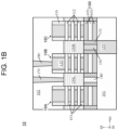
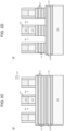
- FIG. 1A illustrates a top plan view of a semiconductor device including a self-aligned backside contact structure, according to an embodiment.
- FIG. 1B illustrates a cross-section view of the semiconductor device of FIG. 1A along a line I-I' shown therein in a D1 direction, according to an embodiment.
- the D1 direction is a channel-length direction which intersects a D2 direction, which is a channel-width direction, and a D3 direction which is a vertical direction.
- a semiconductor device 10 may include 1 st to 3 rd semiconductor stacks 10A-10C each of which may include a plurality of channel layers 112 vertically stacked on a front side of the semiconductor device 10 and surrounded by a gate structure 115. Each of the channel layers 112 may be referred to as a nanosheet or nanoribbon. Each of the semiconductor stacks 10A-10C may also include an isolation stack 100 including a couple of isolation layers 103 and a substrate layer 105 therebetween. A backside isolation structure 161 may be formed below the semiconductor stacks 10A-10C.
- the channel layers 112 of each of the semiconductor stacks 10A-10C surrounded by the gate structure 115 may form a channel structure which connects source/drain regions formed at both sides of the channel structure to each other to form a field-effect nanosheet transistor.
- a field-effect nanosheet transistor may be formed by a channel structure including the channel layers 112, the gate structure 115 surrounding the channel structure, and 1 st and 2 nd source/drain regions 130L and 130R connected to each other by the channel structure.
- One or more materials forming the channel layers 112 may include, for example, silicon (Si), silicon germanium (SiGe).
- the gate structure 115 may be formed of one or more materials including, for example, copper (Cu), aluminum (Al), cobalt (Co), tungsten (W), titanium (Ti), tantalum (Ta) or their combination.
- Each of the source/drain regions 130L and 130R may include one or more materials, for example, silicon (Si), silicon germanium (SiGe) doped with impurities.
- the source/drain regions 130L and 130R may be either a p-type or an n-type.
- Each of the semiconductor stacks 10A-10C may also include inner spacers 131 formed at side surfaces of lower portions of the gate structure 115 and gate spacers 116 formed at side surfaces of an upper portion of the gate structure 115.
- the inner spacers 131 may isolate the gate structure 115 from the source/drain regions 130L and 130R, and the gate spacers 116 may isolate the gate structure 115 from the source/drain regions 130L and 130R and other frontside isolation structure 162.
- One or more materials forming the inner spacers 131 and the gate spacers 116 may include, for example, silicon oxide (e.g., SiO 2 ) or silicon nitride (Si 3 N 4 ).
- the frontside isolation structure 162 may be formed of, for example, silicon oxide (e.g., SiO or SiO 2 ).
- the semiconductor device 10 may also include a plurality of contact structures including a frontside contact structure 170, a gate contact structure 180, and a backside contact structure 150.
- the frontside contact structure 170 may be formed on a top surface of the 1 st source/drain region 130L to connect this source/drain region to a voltage source or another semiconductor device.
- the gate contact structure 180 may be formed on a top surface of the gate structure 115 to receive a gate input signal for the gate structure 115.
- the frontside contact structure 170 and the gate contact structure 180 may be isolated from each other though the frontside isolation structure 162.
- the backside contact structure 150 may be formed on a bottom surface of the 2 nd source/drain region 130R to connect this source/drain region to a voltage source or another semiconductor device.
- These contact structures 170, 180 and 150 may each be formed of one or more materials such as copper (Cu), aluminum (Al), tungsten (W), ruthenium (Ru), molybdenum (Mo), etc.
- the semiconductor device 10 may be characterized by the isolation stack 100 formed at the lower portion of each of the semiconductor stacks 10A-10C.
- the isolation stack 100 may include the two isolation layers 103 and the substrate layer 105 disposed therebetween.
- the uppermost isolation layer among the isolation layers 103 may be formed below the lowermost portion of the gate structure 115 and the lowermost inner spacers among the inner spacers 131.
- the uppermost isolation layer 103 may suppress current leakage from the gate structure 115 thereabove.
- the isolation layers 103 with the substrate layer 105 therebetween may also structurally support each of the semiconductor stacks 10A-10C.
- the substrate layer 105 may be formed of silicon (Si), not being limited thereto.
- the isolation layer 103 may be formed a material such as silicon oxide (e.g., SiO 2 ), not being limited thereto.
- FIG. 1B shows that the isolation stack 100 includes two vertically-stacked isolation layers 103 and the substrate layer 105 disposed therebetween.
- the isolation stack 100 may be structurally strengthened to more stably support each of the semiconductor stacks 10A-10C.
- the number of the isolation layers 103 and the substrate layer 105 may be controlled such that an entire thickness of the isolation stack 100 corresponds to or is the same as a thickness of the backside contact structure 150 in the D3 direction.
- the isolation stack 100 may include more than two isolation layers and more than one substrate layer disposed between every two vertically adjacent isolation layers.
- the isolation stack 100 may include only one isolation layer and only one substrate layer having a thickness corresponding to that of the two isolation layers 103 with the substrate layer 105. Still, however, the isolation layer 103 may be formed as a top layer of the isolation stack 100 to prevent current leakage from the gate structure 115 thereabove.
- the semiconductor device 10 may be further characterized by a backside spacer 151 formed at lateral sides of the isolation stack 100.
- the isolation stack 100 comprises the two isolation layers 103 and the substrate layer 105 which are vertically stacked on the backside isolation structure 161
- the backside spacer 151 may contact side surfaces of the isolation layers 103 and the substrate layer 105.
- the backside spacer 151 may be formed such that a top surface thereof is horizontally aligned with or coplanar with a top surface of the backside contact structure 150, a top surface of the uppermost isolation layer 103, and bottom surfaces of the lowermost inner spacer 131 and the gate structure 115.
- the backside spacer 151 may have been used to form the backside contact structure 150 in a self-aligning manner when the semiconductor device 10 was manufactured, which will be further described later.
- the backside contact structure 150 may be formed between the backside spacers 151 formed at side surfaces of two adjacent isolation stacks 100, and connected to a backside metal line 155 formed therebelow in a backside isolation structure 161. As the backside contact structure 150 is self-aligned precisely below each of the source/drain regions 130L and 130R due to the backside spacer 151, the semiconductor device 10 may have an improved backside contact performance.
- the backside spacer 151 may be formed of one or more materials including silicon nitride (e.g., SiN, SiBCN, SiOCN, SiOC, etc.).
- the backside spacer 151, the inner spacers 131 and the gate spacer 116 may the same or different material compositions from each other.
- the backside metal line 155 may be formed of one or more materials such as copper (Cu), aluminum (Al), tungsten (W), ruthenium (Ru), molybdenum (Mo), etc., which may be the same as or different from the materials forming the contact structures 150, 170 and 180.
- the backside isolation structure 161 may be formed of the same material forming the frontside isolation structure 162.
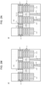
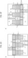
- the preliminary isolation stack 100' may be etched to form three isolation stacks 100 and further extend the recesses R1 and R2 downward to provide a space for formation of a backside contact structure in a later step. Further, the three isolation stacks 100 patterned from the preliminary isolation stack 100' along with the three channel stacks 110 now form 1 st to 3 rd intermediate semiconductor stacks 10A'-10C'.
- the etching operation in this step may be performed through, for example, selective wet etching or dry etching, not being limited thereto, remove only silicon germanium included in the 2 nd sacrificial layers 111 against silicon included in the channel layers 112, the substrate layer 105 and silicon oxide included in the isolation layers 103.
- selective wet etching or dry etching not being limited thereto, remove only silicon germanium included in the 2 nd sacrificial layers 111 against silicon included in the channel layers 112, the substrate layer 105 and silicon oxide included in the isolation layers 103.
- a mixture of hydrofluoric acid (HF) and nitric acid (HNO 3 ) may be used for the selective etching.
- Each of the inner spacer 131 may be formed such that an outer side surface opposite to an inner side surface contacting the dented 2 nd sacrificial layer 111 is vertically aligned with or coplanar with the side surfaces of the channel layers 112 and the isolation stack 100.
- the backside spacer 151 may be conformally formed on an outer surface of each of the intermediate semiconductor stacks 10A'-10C' including the side surfaces of each of the isolation stacks 100.
- the formation of the inner spacers 131 and the backside spacers 151 may be performed through, for example, atomic layer deposition (ALD) or any other suitable deposition process or electroplating.
- ALD atomic layer deposition
- the placeholder structure 140 may be formed to have the same thickness as the isolation stack 100 in the D3 direction.
- the placeholder structure 140 may include a material such as silicon germanium (SiGe) or silicon oxide (e.g., SiO, SiO 2 , etc.), not being limited thereto.
- the formation of the placeholder structure 140 in the lower portion of each of the recesses R1 and R2 may be performed through, for example, CVD, PVD, PECVD, ALD, or a combination thereof, not being limited thereto.
- the etch back of the backside spacer 151 may be performed through, for example, dry etching, not being limited thereto, such that the top surfaces thereof are horizontally aligned or coplanar with the top surfaces of the placeholder structures 140.
- the source/drain regions including the 1 st and 2 nd source/drain regions 130L and 130R may be epitaxially grown from the channel layers 112 on or above the top surfaces of the placeholder structures 140 and the backside spacers 151.
- the removal of the hard mask patterns 160 may be performed through, for example, plasma ashing, stripping, etc. Further, the gate spacer 116 may be etched back so that a top surface thereof may be horizontally aligned or coplanar with a top surface of the dummy gate structure 115' in each of the intermediate semiconductor stacks 10A'-10C'.
- the frontside isolation structure 162 may be formed through, for example, CVD, PVD, PECVD, ALD, or a combination thereof, not being limited thereto, and planarized through, for example, a CMP operation.
- the dummy gate structure 115' and the 2 nd sacrificial layers 111 may be replaced by the gate structure 115, and the frontside contact structure 170 and the gate contact structure 180 may be formed to contact the 1 st source/drain region 130L and the gate structure 115, respectively.
- the dummy gate structure 115' and the 2 nd sacrificial layers 111 may be removed through, for example, wet etching and/or dry etching, to leave voids or spaces in each of the intermediate semiconductor stacks 10A'-10C', and the gate structure 115 may be formed in those voids or spaces through, for example, CVD, PVD, PECVD, ALD, or a combination thereof, not being limited thereto.
- frontside contact structure 170 and the gate contact structure 180 may be performed through a similar deposition process after photolithography/masking/etching operations on the frontside isolation structure 162.
- the intermediate semiconductor device 10' obtained in the previous step may be flipped upside down, and the substrate 101 may be removed and replaced by the backside isolation structure 161, which is patterned to expose the placeholder structure 140 and the backside spacers 151 formed below the 2 nd source/drain region 130R.
- a carrier substrate may be formed on a top surface of the intermediate semiconductor device 10' obtained in the previous step before the intermediate semiconductor device 10' is flipped upside down for a backside process.
- the substrate 101 may be removed through, for example, dry etching, wet etching, ashing and/or stripping, and the backside isolation structure 161 may be formed through, for example, PVD, CVD, PECVD, etc. not being limited thereto, followed by planarization.
- the backside isolation structure 161 may be patterned through, for example, photolithography/masking/etching to expose the bottom surfaces of the placeholder structure 140 and the backside spacer 151 on which a subsequent backside process is to be performed in a next step. It is to be understood here that in FIG. 2J , the bottom surfaces of the placeholder structure 140 and the backside spacer 151 are shown as top surfaces thereof because the intermediate semiconductor device 10' has been inverted for a backside process.
- the placeholder structure 140 formed on the bottom surface of the 2 nd source/drain region 130R between the backside spacers 151 may be removed through selective etching against the backside spacers 151 based on the photoresist pattern.
- the selective etching of the placeholder structure 140 including, for example, silicon germanium or silicon oxide against the backside spacers 151 including, for example, silicon nitride may be wet etching and/or dry etching using an etchant such as hot phosphoric acid (H3PO4) or potassium hydroxide (KOH), not being limited thereto.
- an etchant such as hot phosphoric acid (H3PO4) or potassium hydroxide (KOH), not being limited thereto.
- the backside contact structure 150 may be formed in a void or space, from which the placeholder structure 140 has been removed in the previous step, in a self-aligning manner based on the backside spacers 151.
- a metal such as copper (Cu), aluminum (Al), tungsten (W), ruthenium (Ru), molybdenum (Mo), etc. may be deposited in the void or space through, for example, CVD, PVD, PECVD or a combination thereof, not being limited thereto. Due to the backside spacers 151 formed at both sides of the void or space left from the removal of the placeholder structure 140, the metal deposited in the void or space may be self-aligned with the bottom surface (top surface in FIG. 2M ) of the 2 nd source/drain region 130R.
- the backside contact structure 150 may have the same shape as the placeholder structure 140.
- a thickness of the backside contact structure 150 may be the same as that of the placeholder structure 140 in the D3 direction.
- the backside metal line 155 may be formed to be connected to the backside contact structure 150 to finish a BSPDN of the intermediate semiconductor device 10'
- a metal similar to that forming the backside contact structure 150 may be deposited through, for example, CVD, PVD, PECVD or a combination thereof, to form the backside metal line 155 which connects the 2 nd source/drain region 130R to a voltage source or another circuit element for internal routing purposes.
- the intermediate semiconductor device 10' obtained in the previous step may be flipped upside down again to finish the manufacturing operation for the semiconductor device 10 at least in part.
- FIG. 3 illustrates a flowchart describing a method of manufacturing a semiconductor device including a self-aligned contact structure in reference to FIGS. 2A-2P , according to embodiments.
- a preliminary isolation stack including two or more vertically-stacked isolation layers and a substrate layer therebetween may be formed between a substrate therebelow and a plurality of channel stacks thereabove, to form an intermediate semiconductor device. See FIGS. 2A-2C .
- the isolation layers may be formed of a material including silicon oxide, which may more etching prone than silicon.
- a number of the isolation layers and a vertical thickness of the isolation stack may be controlled to correspond to or be the same as a vertical thickness of a backside contact structure to be formed in a later step.
- the preliminary isolation stack may be etched down between the channel stacks to form a plurality of isolation stacks, respectively below the channel stacks, and recesses in which respective placeholder structures for backside contact structures are to be formed. See FIGS. 2D-2F .
- the preliminary isolation stack includes the isolation layers formed of silicon oxide which is etching prone, it may be possible to etch out a hole or recess having a profile for easy deposition of a metal for a backside contact structure.
- backside spacers may be formed on side surfaces of the recesses for the placeholder structures, which will facilitate self-aligned formation of backside contact structures in a later step. See FIG. 2G .
- the backside spacer may be formed to contact side surfaces of each of the isolation stacks.
- the backside spacer may be formed of a material such as silicon nitride.
- the placeholder structures may be formed in the recesses between the backside spacers. See FIG. 2H .
- the placeholder structure may be formed of a material such as silicon germanium or silicon oxide.
- source/drain regions may be formed from the channel stacks at sides of the channel stacks on or above the placeholder structures and the backside spacers, and a gate structure may be formed to surround the channel stack. See FIGS. 2I-2K .
- the substrate may be removed and replaced by a backside isolation structure, and the backside isolation structure may be patterned to expose at least one of the placeholder structure and the backside spacers thereon. See FIG. 2L .
- the removal of the substrate and the formation of the backside isolation structure may be performed after inverting the intermediate semiconductor device obtained in the previous step such that a bottom surface of the substrate is directed upward in the D3 direction.
- a backside metal line may be formed to contact the backside contact structure in the backside isolation structure to at least partially finish a BSPDN of a semiconductor device. See FIGS. 2O-2P .
- FIG. 4 is a schematic block diagram illustrating an electronic device including one or more semiconductor devices including a self-aligned backside contact structure as shown in FIGS. 1A and 1B , according to embodiments.
- an electronic device 4000 may include at least one application processor 4100, a communication module 4200, a display/touch module 4300, a storage device 4400, and a buffer RAM 4500.
- the electronic device 4000 may be a mobile device such as a smartphone or a tablet computer, not being limited thereto, according to embodiments.
- the application processor 4100 may control operations of the electronic device 4000.
- the communication module 4200 is implemented to perform wireless or wire communications with an external device.
- the display/touch module 4300 is implemented to display data processed by the application processor 4100 and/or to receive data through a touch panel.
- the storage device 4400 is implemented to store user data.
- the storage device 4400 may be an embedded multimedia card (eMMC), a solid state drive (SSD), a universal flash storage (UFS) device, etc.
- eMMC embedded multimedia card
- SSD solid state drive
- UFS universal flash storage
- the storage device 4400 may perform caching of the mapping data and the user data as described above.
- the buffer RAM 4500 may temporarily store data used for processing operations of the electronic device 4000.
- the buffer RAM 4500 may be volatile memory such as double data rate (DDR) synchronous dynamic random access memory (SDRAM), low power double data rate (LPDDR) SDRAM, graphics double data rate (GDDR) SDRAM, Rambus dynamic random access memory (RDRAM), etc.
- DDR double data rate
- LPDDR low power double data rate
- GDDR graphics double data rate SDRAM
- RDRAM Rambus dynamic random access memory
- At least one component in the electronic device 4000 may include one or more semiconductor devices including a self-aligned backside contact structure as shown in FIGS. 1A and 1B .
Landscapes
- Engineering & Computer Science (AREA)
- Chemical & Material Sciences (AREA)
- Nanotechnology (AREA)
- Physics & Mathematics (AREA)
- Insulated Gate Type Field-Effect Transistor (AREA)
- Crystallography & Structural Chemistry (AREA)
- Theoretical Computer Science (AREA)
- Mathematical Physics (AREA)
- Thin Film Transistor (AREA)
- Condensed Matter Physics & Semiconductors (AREA)
- General Physics & Mathematics (AREA)
- Computer Hardware Design (AREA)
- Microelectronics & Electronic Packaging (AREA)
- Power Engineering (AREA)
- Electrodes Of Semiconductors (AREA)
- Element Separation (AREA)
Applications Claiming Priority (2)
| Application Number | Priority Date | Filing Date | Title |
|---|---|---|---|
| US202363522522P | 2023-06-22 | 2023-06-22 | |
| US18/375,186 US20240429130A1 (en) | 2023-06-22 | 2023-09-29 | Semiconductor device including self-aligned backside contact structure |
Publications (2)
| Publication Number | Publication Date |
|---|---|
| EP4480903A2 true EP4480903A2 (de) | 2024-12-25 |
| EP4480903A3 EP4480903A3 (de) | 2025-04-23 |
Family
ID=91581851
Family Applications (1)
| Application Number | Title | Priority Date | Filing Date |
|---|---|---|---|
| EP24182532.2A Pending EP4480903A3 (de) | 2023-06-22 | 2024-06-17 | Halbleiterbauelement mit selbstausgerichteter rückseitenkontaktstruktur |
Country Status (5)
| Country | Link |
|---|---|
| US (1) | US20240429130A1 (de) |
| EP (1) | EP4480903A3 (de) |
| KR (1) | KR20240178667A (de) |
| CN (1) | CN119181706A (de) |
| TW (1) | TW202520481A (de) |
Cited By (1)
| Publication number | Priority date | Publication date | Assignee | Title |
|---|---|---|---|---|
| EP4553836A1 (de) * | 2023-11-06 | 2025-05-14 | Samsung Electronics Co., Ltd. | Halbleiterbauelement mit selbstausgerichteter rückseitenkontaktstruktur und ätzstoppschicht |
Family Cites Families (8)
| Publication number | Priority date | Publication date | Assignee | Title |
|---|---|---|---|---|
| US11830773B2 (en) * | 2020-02-26 | 2023-11-28 | Taiwan Semiconductor Manufacturing Co., Ltd. | Semiconductor device with isolation structures |
| US11410930B2 (en) * | 2020-04-28 | 2022-08-09 | Taiwan Semiconductor Manufacturing Co., Ltd. | Semiconductor device and method |
| US11626494B2 (en) * | 2020-06-17 | 2023-04-11 | Taiwan Semiconductor Manufacturing Co., Ltd. | Epitaxial backside contact |
| US12205997B2 (en) * | 2021-03-12 | 2025-01-21 | Taiwan Semiconductor Manufacturing Co., Ltd. | Integrated circuit including backside conductive vias |
| US11482595B1 (en) * | 2021-04-23 | 2022-10-25 | Taiwan Semiconductor Manufacturing Co., Ltd. | Dual side contact structures in semiconductor devices |
| US12119348B2 (en) * | 2021-04-28 | 2024-10-15 | Taiwan Semiconductor Manufacturing Company Limited | Stacked device structures and methods for forming the same |
| US20220359679A1 (en) * | 2021-05-05 | 2022-11-10 | Taiwan Semiconductor Manufacturing Co., Ltd. | Backside source/drain contacts and methods of forming the same |
| US12136655B2 (en) * | 2021-09-22 | 2024-11-05 | International Business Machines Corporation | Backside electrical contacts to buried power rails |
-
2023
- 2023-09-29 US US18/375,186 patent/US20240429130A1/en active Pending
-
2024
- 2024-05-13 KR KR1020240062732A patent/KR20240178667A/ko active Pending
- 2024-06-17 EP EP24182532.2A patent/EP4480903A3/de active Pending
- 2024-06-20 TW TW113122962A patent/TW202520481A/zh unknown
- 2024-06-21 CN CN202410807875.6A patent/CN119181706A/zh active Pending
Cited By (1)
| Publication number | Priority date | Publication date | Assignee | Title |
|---|---|---|---|---|
| EP4553836A1 (de) * | 2023-11-06 | 2025-05-14 | Samsung Electronics Co., Ltd. | Halbleiterbauelement mit selbstausgerichteter rückseitenkontaktstruktur und ätzstoppschicht |
Also Published As
| Publication number | Publication date |
|---|---|
| CN119181706A (zh) | 2024-12-24 |
| US20240429130A1 (en) | 2024-12-26 |
| TW202520481A (zh) | 2025-05-16 |
| KR20240178667A (ko) | 2024-12-31 |
| EP4480903A3 (de) | 2025-04-23 |
Similar Documents
| Publication | Publication Date | Title |
|---|---|---|
| CN110800113B (zh) | 埋入式电力轨道 | |
| EP4270458A1 (de) | Via zur verbindung der vorderseite einer halbleitervorrichtung mit einem rückseitigen stromverteilungsnetzwerk und zugehöriges verfahren | |
| EP4468332A1 (de) | Halbleiterbauelement mit rückseitiger source-/drain-kontaktstruktur mit kontaktabstandhalter und rückseitiger gate-kontaktstruktur | |
| EP4421859A1 (de) | Halbleiterbauelement mit auf basis einer kontaktisolationsschicht geformter selbstausgerichteter rückseitenkontaktstruktur | |
| EP4480903A2 (de) | Halbleiterbauelement mit selbstausgerichteter rückseitenkontaktstruktur | |
| CN119108396A (zh) | 半导体器件和制造半导体器件的方法 | |
| EP4525584A2 (de) | 3d-gestapelte halbleitervorrichtung und verfahren zur herstellung davon | |
| EP4495986A1 (de) | 3d-gestapelte halbleitervorrichtung und verfahren zur herstellung davon | |
| EP4421862A1 (de) | Halbleiteranordnung mit 3d-stapel-feldeffekttransistoren mit isolationsstruktur zwischen den kontakten | |
| US20240274676A1 (en) | Semiconductor device including backside contact structure having low ohmic contact resistance | |
| EP4553836A1 (de) | Halbleiterbauelement mit selbstausgerichteter rückseitenkontaktstruktur und ätzstoppschicht | |
| EP4651196A1 (de) | Halbleiterbauelement mit rückseitiger kontaktstruktur, die auf der basis einer breiten platzhalterstruktur gebildet wird | |
| US20240290853A1 (en) | Semiconductor device including extended backside contact structure | |
| US20250316594A1 (en) | Semiconductor device including backside contact structure formed based on wide placeholder structure | |
| US12389660B1 (en) | Semiconductor device including backside contact structure with silicide layer formed in FEOL process | |
| EP4608091A2 (de) | Halbleiterbauelement mit gabelschichttransistoren mit isolationswand und gate-schnitt-struktur darauf | |
| EP4633321A1 (de) | Halbleiterbauelement mit rückseitiger kontaktstruktur mit in einem feol-prozess geformter silizidschicht | |
| US20250098324A1 (en) | 3d-stacked semiconductor device having different channel structures, source/drain regions, and gate structures at different levels | |
| US20240290689A1 (en) | Semiconductor device including backside contact structure | |
| US20250275234A1 (en) | Semiconductor device including forksheet transistor structure and early-formed gate cut structure | |
| US20250254989A1 (en) | Semiconductor device including different inner spacers | |
| CN118553768A (zh) | 包括扩展背侧接触结构的半导体器件及其制造方法 |
Legal Events
| Date | Code | Title | Description |
|---|---|---|---|
| PUAI | Public reference made under article 153(3) epc to a published international application that has entered the european phase |
Free format text: ORIGINAL CODE: 0009012 |
|
| STAA | Information on the status of an ep patent application or granted ep patent |
Free format text: STATUS: THE APPLICATION HAS BEEN PUBLISHED |
|
| AK | Designated contracting states |
Kind code of ref document: A2 Designated state(s): AL AT BE BG CH CY CZ DE DK EE ES FI FR GB GR HR HU IE IS IT LI LT LU LV MC ME MK MT NL NO PL PT RO RS SE SI SK SM TR |
|
| PUAL | Search report despatched |
Free format text: ORIGINAL CODE: 0009013 |
|
| AK | Designated contracting states |
Kind code of ref document: A3 Designated state(s): AL AT BE BG CH CY CZ DE DK EE ES FI FR GB GR HR HU IE IS IT LI LT LU LV MC ME MK MT NL NO PL PT RO RS SE SI SK SM TR |
|
| RIC1 | Information provided on ipc code assigned before grant |
Ipc: H01L 29/775 20060101ALI20250319BHEP Ipc: H01L 29/66 20060101ALI20250319BHEP Ipc: H01L 29/417 20060101ALI20250319BHEP Ipc: H01L 29/10 20060101ALI20250319BHEP Ipc: H01L 29/06 20060101ALI20250319BHEP Ipc: H01L 21/8234 20060101ALI20250319BHEP Ipc: B82Y 10/00 20110101AFI20250319BHEP |
|
| STAA | Information on the status of an ep patent application or granted ep patent |
Free format text: STATUS: REQUEST FOR EXAMINATION WAS MADE |
|
| 17P | Request for examination filed |
Effective date: 20250520 |