EP4478842A1 - Printed circuit board assembly and method for manufacturing printed circuit board assembly - Google Patents
Printed circuit board assembly and method for manufacturing printed circuit board assembly Download PDFInfo
- Publication number
- EP4478842A1 EP4478842A1 EP24173870.7A EP24173870A EP4478842A1 EP 4478842 A1 EP4478842 A1 EP 4478842A1 EP 24173870 A EP24173870 A EP 24173870A EP 4478842 A1 EP4478842 A1 EP 4478842A1
- Authority
- EP
- European Patent Office
- Prior art keywords
- circuit board
- printed circuit
- plate portion
- metal frame
- supports
- Prior art date
- Legal status (The legal status is an assumption and is not a legal conclusion. Google has not performed a legal analysis and makes no representation as to the accuracy of the status listed.)
- Granted
Links
Images




Classifications
-
- H—ELECTRICITY
- H05—ELECTRIC TECHNIQUES NOT OTHERWISE PROVIDED FOR
- H05K—PRINTED CIRCUITS; CASINGS OR CONSTRUCTIONAL DETAILS OF ELECTRIC APPARATUS; MANUFACTURE OF ASSEMBLAGES OF ELECTRICAL COMPONENTS
- H05K7/00—Constructional details common to different types of electric apparatus
- H05K7/14—Mounting supporting structure in casing or on frame or rack
- H05K7/1417—Mounting supporting structure in casing or on frame or rack having securing means for mounting boards, plates or wiring boards
- H05K7/142—Spacers not being card guides
-
- H—ELECTRICITY
- H05—ELECTRIC TECHNIQUES NOT OTHERWISE PROVIDED FOR
- H05K—PRINTED CIRCUITS; CASINGS OR CONSTRUCTIONAL DETAILS OF ELECTRIC APPARATUS; MANUFACTURE OF ASSEMBLAGES OF ELECTRICAL COMPONENTS
- H05K1/00—Printed circuits
- H05K1/02—Details
-
- H—ELECTRICITY
- H05—ELECTRIC TECHNIQUES NOT OTHERWISE PROVIDED FOR
- H05K—PRINTED CIRCUITS; CASINGS OR CONSTRUCTIONAL DETAILS OF ELECTRIC APPARATUS; MANUFACTURE OF ASSEMBLAGES OF ELECTRICAL COMPONENTS
- H05K1/00—Printed circuits
- H05K1/02—Details
- H05K1/0271—Arrangements for reducing stress or warp in rigid printed circuit boards, e.g. caused by loads, vibrations or differences in thermal expansion
-
- H—ELECTRICITY
- H05—ELECTRIC TECHNIQUES NOT OTHERWISE PROVIDED FOR
- H05K—PRINTED CIRCUITS; CASINGS OR CONSTRUCTIONAL DETAILS OF ELECTRIC APPARATUS; MANUFACTURE OF ASSEMBLAGES OF ELECTRICAL COMPONENTS
- H05K3/00—Apparatus or processes for manufacturing printed circuits
-
- H—ELECTRICITY
- H05—ELECTRIC TECHNIQUES NOT OTHERWISE PROVIDED FOR
- H05K—PRINTED CIRCUITS; CASINGS OR CONSTRUCTIONAL DETAILS OF ELECTRIC APPARATUS; MANUFACTURE OF ASSEMBLAGES OF ELECTRICAL COMPONENTS
- H05K2201/00—Indexing scheme relating to printed circuits covered by H05K1/00
- H05K2201/10—Details of components or other objects attached to or integrated in a printed circuit board
- H05K2201/10227—Other objects, e.g. metallic pieces
- H05K2201/10424—Frame holders
Definitions
- Embodiments relate to a printed circuit board assembly and a method for manufacturing a printed circuit board assembly.
- PCB printed circuit board
- Embodiments are directed to a printed circuit board assembly, including a printed circuit board having a plurality of support holes, a metal frame supporting the printed circuit board, and a plurality of bonding portions between the metal frame and the printed circuit board bonding the metal frame and the printed circuit board, wherein the metal frame includes a plate portion opposite the printed circuit board, and a plurality of supports that is integral with the plate portion, bent and extending from the plate portion to the printed circuit board, inserted into the plurality of support holes, and supporting the printed circuit board.
- the metal frame may further include a plurality of through-holes adjacent to the plurality of supports and penetrating the plate portion.
- a planar shape of the plurality of through-holes may be the same as a side shape of the plurality of supports.
- the number of the plurality of through-holes may be the same as the number of the plurality of supports.
- the plurality of supports may be separated from the plurality of through-holes and may be bent from the plate portion to protrude from the plate portion.
- the metal frame may further include a plurality of through-hinges penetrating between the plurality of supports and the plate portion.
- the metal frame may further comprise a plurality of connecting hinges that curve and connect between each of the plurality of supports and the plate portion with each of the plurality of through-hinges interposed therebetween.
- the plurality of through-hinges may be linear.
- each of the plurality of supports may include an insertion portion inserted into each of the plurality of support holes, and a support portion may extend from the insertion portion to the plate portion and supporting the printed circuit board.
- the support portion may include a side portion extending at an incline from the plate portion toward the printed circuit board, and an upper portion positioned between the side portion and the insertion portion and contacting the printed circuit board.
- each of the plurality of bonding portions may have a different thickness.
- each of the plurality of bonding portions may have a different area.
- each of the plurality of bonding portions may include solder.
- the plurality of supports may be closer to a corner of the plate portion than to a center of the plate portion.
- a method for manufacturing a printed circuit board assembly includes separating a plurality of supports from a plate portion of a metal frame and bending the plurality of supports from the plate portion to protrude from the plate portion, supporting the printed circuit board on the metal frame by inserting the plurality of supports into a plurality of support holes of the printed circuit board, and bonding the metal frame and the printed circuit board using a plurality of bonding portions between the metal frame and the printed circuit board.
- the separating of the plurality of supports from the plate portion of the metal frame and bending the plurality of supports from the plate portion to protrude from the plate portion may include forming a plurality of through-holes adjacent to the plurality of supports and penetrating the plate portion on the metal frame.
- the separating of the plurality of supports from the plate portion of the metal frame and bending the plurality of supports from the plate portion to protrude from the plate portion may be performed by separating the plurality of supports from the plurality of through-holes along a plurality of through-hinges penetrating between the plurality of supports and the plate portion, and bending the plurality of supports from the plate portion.
- the plurality of through-hinges may be linear.
- the bonding of the metal frame and the printed circuit board by positioning the plurality of bonding portions between the metal frame and the printed circuit board may be performed by soldering the plurality of bonding portions between the metal frame and the printed circuit board.
- each of the plurality of bonding portions may have a different thickness.
- a printed circuit board assembly and a method for manufacturing the printed circuit board assembly in which a short circuit between the metal frame and the printed circuit board is suppressed by maintaining a constant distance between the metal frame and the printed circuit board, even if no separate structure is added between the metal frame and the printed circuit board, are provided.
- the printed circuit board assembly may be a printed circuit board assembly included in a protective circuit module of a secondary battery, but is not limited thereto, and may be a printed circuit board assembly including a printed circuit board assembly and a metal frame included in various known electronic devices.
- FIG. 1 is a cross-sectional view illustrating a printed circuit board assembly according to an embodiment.
- a printed circuit board assembly 1000 may include a printed circuit board 100, a metal frame 200, and a plurality of bonding portions 300.
- the printed circuit board 100 may include a plurality of support holes 110 positioned on the outside and a plurality of chips 120 mounted on the printed circuit board 100.
- the plurality of support holes 110 may be positioned at corners of the printed circuit board 100 in a plan view, but are not limited thereto.
- a plurality of support holes 110 may penetrate the printed circuit board 100.
- a plurality of supports 220 of the metal frame 200 may be inserted into the plurality of support holes 110.
- the plurality of support holes 110 may have various planar shapes corresponding to the shapes of the plurality of supports 220.
- the plurality of support holes 110 may have various planar shapes such as polygons, including triangles, quadrangles, pentagons, and hexagons, as well as circular shapes, oval shapes, and irregular shapes.
- the plurality of chips 120 may be mounted on the printed circuit board 100.
- the plurality of chips 120 may include various known electronic chips included in various known protective circuit modules of secondary batteries, but are not limited thereto, and may include electronic chips included in various known electronic devices.
- the metal frame 200 may be bonded to the printed circuit board 100 using a plurality of bonding portions 300 therebetween.
- the metal frame 200 supports the printed circuit board 100.
- the metal frame 200 may have an area corresponding to the area of the printed circuit board 100, but is not limited thereto.
- the metal frame 200 may have an area and a structure corresponding to a region inside a case of the secondary battery on which the printed circuit board assembly included in the protective circuit module of the secondary battery is mounted. In some embodiments, the metal frame 200 may have an area and structure corresponding to a region of various known electronic devices.
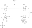
- FIG. 2 is a top plan view illustrating a metal frame of a printed circuit board assembly according to an embodiment.
- FIG. 3 is a side view illustrating a metal frame of a printed circuit board assembly according to an embodiment.
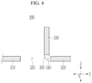
- FIG. 4 is a cross-sectional view along IV-IV line of FIG. 2 .
- the metal frame 200 includes a plate portion 210, a plurality of supports 220, a plurality of through-holes 230, a plurality of through-hinges 240, and a plurality of connecting hinges 250.
- the plate portion 210 may be opposite to or face-to-face with the printed circuit board 100.
- the plate portion 210 may include a metal containing nickel (Ni), but is not limited thereto.
- the plate portion 210 may include various known metals such as aluminum (Al) and stainless steel.
- the plate portion 210 may have a plate shape extending in a first direction X and in a second direction Y intersecting with the first direction X, but is not limited thereto.
- the plate portion 210 may be opposite to or face-to-face with the printed circuit board 100 in a third direction Z intersecting with the first and second directions X and Y.
- the plate portion 210 may be integral with the plurality of supports 220.
- the plurality of supports 220 integral with the plate portion 210, may be bent and extend from the plate portion 210 to the printed circuit board 100 and inserted into the plurality of support holes 110 of the printed circuit board 100, to support the printed circuit board 100.
- the plurality of supports 220 support the printed circuit board 100, so that the printed circuit board 100 is supported on the metal frame 200 while maintaining a certain distance from the metal frame 200.
- the plurality of supports 220 may be bent and extend in the third direction Z from the plate portion 210 and inserted into the plurality of support holes 110 of the printed circuit board 100.
- the plurality of supports 220 may extend in the first direction X and the second direction Y inside the plurality of through-holes 230 of the plate portion 210, and are separated from the plurality of through-holes 230, bent in the third direction Z from the plate portion 210, and may protrude and extend from the plate portion 210 in the third direction Z.
- the plurality of supports 220 may be positioned closer to the corners of the first direction X and the second direction Y of the plate portion 210 than to the center of the first direction X and the second direction Y of the plate portion 210, and may be positioned at the corners of the plate portion 210.
- Each of the plurality of supports 220 may include an insertion portion 221 and a support portion 222.
- the insertion portion 221 may be inserted into each of the plurality of support holes 11 0 of the printed circuit board 100.
- the insertion portion 221 may protrude from the support portion 222 in the third direction Z.
- a planar shape of the insertion portion 221 may have the same shape as that of the support hole 110, but is not limited thereto.
- the support portion 222 may extend from the insertion portion 221 to the plate portion 210.
- the support portion 222 may be positioned between the plate portion 210 and the insertion portion 221 and may contact the rear surface of the printed circuit board 100 in the third direction Z to support the printed circuit board 100.
- the support portion 222 may include a side portion 222a and an upper portion 222b.
- the side portion 222a may extend at an incline from the plate portion 210 toward the printed circuit board 100.
- the side portion 222a may extend at an incline from the front surface of the plate portion 210 based on the third direction Z.
- the upper portion 222b may be positioned between the side portion 222a and the insertion portion 221 and may contact the rear surface of the printed circuit board 100 in the third direction Z.
- the side portion 222a of the support portion 222 extends inclined from the upper portion 222b contacting the rear surface of the printed circuit board 100 to the front surface of the plate portion 210, so that the printed circuit board 100 is firmly supported to the support 220.
- the plurality of through-holes 230 may be positioned adjacent to the plurality of supports 220.
- the plurality of through-holes 230 may penetrate the plate portion 210 in the third direction Z.
- the planar shape of the plurality of through-holes 230 may be the same as the side shape of the plurality of supports 220.
- the number of the plurality of through-holes 230 may be the same as the number of the plurality of supports 220.
- the plurality of supports 220 may be separated from the plurality of through-holes 230 and may be bent and may be extended in the third direction Z from the plate portion 210, so that the planar shape of the plurality of through-holes 230 is the same as the side shape of the plurality of supports 220, and the number of the plurality of through-holes 230 is the same as the number of the plurality of supports 220.
- the plurality of through-hinges 240 are shown in FIG. 4 and FIGS. 6 and 7 to be described later.
- the plurality of through-hinges 240 may penetrate between the plurality of supports 220 and the plate portion 210 in the third direction Z.
- the plurality of through-hinges 240 may extend linearly in the first direction X.
- Each of the plurality of through-hinges 240 may extend linearly to correspond to a partial region of the plurality of supports 220 in the first direction X.
- the plurality of connecting hinges 250 are shown in FIG. 4 and FIGS. 6 and 7 to be described later.
- the plurality of connecting hinges 250 may connect between the plurality of supports 220 and the plate portion 210.
- Each of the plurality of connecting hinges 250 may connect in a curved manner each of the plurality of supports 220 and the plate portion 210 with each of the plurality of through-hinges 240 therebetween.
- the plurality of supports 220 may be separated from the plurality of through-holes 230 by the plurality of connecting hinges 250 and the plurality of through-hinges 240 so as to be easily bent and extended from the plate portion 210 in the third direction Z.
- the metal frame 200 and the printed circuit board 100 may be bonded by the plurality of bonding portions 300.
- the plurality of bonding portions 300 may be positioned between the metal frame 200 and the printed circuit board 100.
- the plurality of bonding portions 300 may bond between the metal frame 200 and the printed circuit board 100.
- Each of the plurality of bonding portions 300 may include solder.
- Each of the plurality of bonding portions 300 may have a different thickness due to inherent characteristics of solder formed by a soldering process.
- Each of the plurality of bonding portions 300 may have different an area due to inherent characteristics of solder formed by a soldering process.
- the printed circuit board assembly 1000 may include a metal frame 200, including a plurality of supports 220 that may be integral with the metal frame 200 and that may be bent and extend toward the printed circuit board 100 and that may be inserted into the plurality of support holes 110 of the printed circuit board 100 to support the printed circuit board 100. Accordingly, the printed circuit board 100 may be supported on the metal frame 200 while maintaining a constant distance from the metal frame 200, even if deviation occurs in the thickness and area of each of the plurality of bonding portions 300 bonding between the metal frame 200 and the printed circuit board 100.
- a short circuit between the metal frame 200 and the printed circuit board 100 may be suppressed by maintaining a constant distance between the metal frame 200 and the printed circuit board 100, even if deviation occurs in the thickness and area of each of the plurality of bonding portions 300 because the plurality of bonding portions 300 include solder.
- a printed circuit board assembly 1000 in which the plurality of supports 220 integral with the metal frame 200 bend and extend from the metal frame 200 toward the printed circuit board 100 to support the printed circuit board 100, such that a short circuit between the metal frame 200 and the printed circuit board 100 are suppressed by maintaining a constant distance between the metal frame 200 and the printed circuit board 100, even if no separate structure is added between the metal frame 200 and the printed circuit board 100.
- the printed circuit board assembly according to the above-described embodiment may be manufactured using a method for manufacturing a printed circuit board assembly according to another embodiment, but is not limited thereto.
- FIG. 5 is a flowchart illustrating a method for manufacturing a printed circuit board assembly according to an embodiment.
- FIGS. 6 and 7 are plan views of a metal frame for explaining or describing a method for manufacturing a printed circuit board assembly according to an embodiment.
- the plurality of supports 220 may be separated from the plate portion 210 of the metal frame 200 and may be bent from the plate portion 210 so as to protrude (S100) from the plate portion 210.
- the plurality of through-holes 230 that may be adjacent to the plurality of supports 220 and that may penetrate the plate portion 210 are formed on the metal frame 200.
- the plurality of through-holes 230 may be formed along the edges of the plurality of supports 220, and the plurality of supports 220 may be integrally formed with the metal frame 200 in the same shape as the plurality of through-holes 230.
- the plurality of through-hinges 240 may be formed to linearly penetrate between the plurality of supports 220 and the plate portion 210 in the first direction X.
- the plurality of connecting hinges 250 may be formed to be spaced apart in the first direction X with the through-hinge 240 therebetween according to the formation of the plurality of through hinges 240 to connect the plate portion 210 and the plurality of supports 220.
- the plurality of supports 220 may be separated from the plurality of through-holes 230 based on a bending line CL, that may be in an extending direction of the plurality of through-hinges 240 penetrating between the plurality of supports 220 and the plate portion 210, and bent CU in the third direction Z that intersects with the first direction X from and at the plate portion 210.
- CL a bending line
- bent CU in the third direction Z and the plate portion 210 may be connected by a plurality of curved or bent connecting hinges 250.
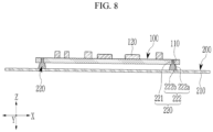
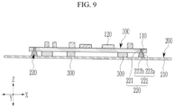
- FIGS. 8 and 9 are cross-sectional views of a printed circuit board assembly for explaining and describing a method for manufacturing a printed circuit board assembly according to an embodiment.
- the plurality of supports 220 may be inserted into the plurality of support holes 110 of the printed circuit board 100 to support the printed circuit board 100 on the metal frame 200 (S200).
- the printed circuit board 100 may be positioned on the metal frame 200, and the plurality of supports 220 of the metal frame 200 may be inserted into the plurality of support holes 110 of the printed circuit board 100 to support the printed circuit board 100 on the plurality of supports 220 of the metal frame 200.
- the printed circuit board 100 may be supported on the metal frame 200 while maintaining a constant distance from the metal frame 200.
- the plurality of bonding portions 300 may be positioned between the metal frame 200 and the printed circuit board 100 to bond between the metal frame 200 and the printed circuit board 100 (S300).
- the metal frame 200 and the printed circuit board 100 may be bonded by soldering a plurality of joints (bonding portions 300) between the metal frame 200 and the printed circuit board 100.
- Each of the plurality of bonding portions 300 may have a different thickness and area due to the inherent characteristics of solder formed by a soldering process, but regardless of the thickness and area of the plurality of bonding portions 300, a constant distance is maintained between the printed circuit board 100 and the metal frame 200 by the plurality of supports 220.
- a printed circuit board included in a protective circuit module of a secondary battery may have the form of a printed circuit board assembly bonded to a metal frame supported inside the case of the secondary battery.
- a conventional printed circuit board assembly may include a metal frame, a printed circuit board bonded to the metal frame, and a plurality of bonding agents bonded between the metal frame and the printed circuit board.
- the conventional printed circuit board assembly has an issue where deviations and variations occur in the distance between the metal frame and the printed circuit board, depending on the difference in thickness of each of a plurality of adhesives positioned therebetween, and various problems and shortcomings of the conventional printed circuit board assembly are avoided by the present printed circuit board assembly that may be made and manufactured as described above.
- the plurality of supports 220 integral with the metal frame 200 may be bent to extend from the metal frame 200 toward the printed circuit board 100 to support the printed circuit board 100, such that a short circuit between the metal frame 200 and the printed circuit board 100 may be suppressed by maintaining a constant distance between the metal frame 200 and the printed circuit board 100, even if no separate structure is added between the metal frame 200 and the printed circuit board 100.
- a method for manufacturing a printed circuit board assembly in which a short circuit between the metal frame 200 and the printed circuit board 100 may be suppressed by maintaining a constant distance between the metal frame 200 and the printed circuit board 100, even if no separate structure is added between the metal frame 200 and the printed circuit board 100.
Landscapes
- Engineering & Computer Science (AREA)
- Microelectronics & Electronic Packaging (AREA)
- Manufacturing & Machinery (AREA)
- Structure Of Printed Boards (AREA)
- Chemical & Material Sciences (AREA)
- Chemical Kinetics & Catalysis (AREA)
- Electrochemistry (AREA)
- General Chemical & Material Sciences (AREA)
- Combinations Of Printed Boards (AREA)
Abstract
Description
- Embodiments relate to a printed circuit board assembly and a method for manufacturing a printed circuit board assembly.
- A printed circuit board (PCB) is used for mounting electronic components.
- Embodiments are directed to a printed circuit board assembly, including a printed circuit board having a plurality of support holes, a metal frame supporting the printed circuit board, and a plurality of bonding portions between the metal frame and the printed circuit board bonding the metal frame and the printed circuit board, wherein the metal frame includes a plate portion opposite the printed circuit board, and a plurality of supports that is integral with the plate portion, bent and extending from the plate portion to the printed circuit board, inserted into the plurality of support holes, and supporting the printed circuit board.
- According to embodiments, the metal frame may further include a plurality of through-holes adjacent to the plurality of supports and penetrating the plate portion.
- According to embodiments, a planar shape of the plurality of through-holes may be the same as a side shape of the plurality of supports.
- According to embodiments, the number of the plurality of through-holes may be the same as the number of the plurality of supports.
- According to embodiments, the plurality of supports may be separated from the plurality of through-holes and may be bent from the plate portion to protrude from the plate portion. According to embodiments, the metal frame may further include a plurality of through-hinges penetrating between the plurality of supports and the plate portion.
- Accordingly to embodiments, the metal frame may further comprise a plurality of connecting hinges that curve and connect between each of the plurality of supports and the plate portion with each of the plurality of through-hinges interposed therebetween.
- According to embodiments, the plurality of through-hinges may be linear.
- According to embodiments, each of the plurality of supports may include an insertion portion inserted into each of the plurality of support holes, and a support portion may extend from the insertion portion to the plate portion and supporting the printed circuit board.
- According to embodiments, the support portion may include a side portion extending at an incline from the plate portion toward the printed circuit board, and an upper portion positioned between the side portion and the insertion portion and contacting the printed circuit board.
- According to embodiments, each of the plurality of bonding portions may have a different thickness.
- According to embodiments, each of the plurality of bonding portions may have a different area.
- According to embodiments, each of the plurality of bonding portions may include solder.
- According to embodiments, the plurality of supports may be closer to a corner of the plate portion than to a center of the plate portion.
- According to embodiments, a method for manufacturing a printed circuit board assembly, includes separating a plurality of supports from a plate portion of a metal frame and bending the plurality of supports from the plate portion to protrude from the plate portion, supporting the printed circuit board on the metal frame by inserting the plurality of supports into a plurality of support holes of the printed circuit board, and bonding the metal frame and the printed circuit board using a plurality of bonding portions between the metal frame and the printed circuit board.
- According to embodiments, the separating of the plurality of supports from the plate portion of the metal frame and bending the plurality of supports from the plate portion to protrude from the plate portion may include forming a plurality of through-holes adjacent to the plurality of supports and penetrating the plate portion on the metal frame.
- According to embodiments, the separating of the plurality of supports from the plate portion of the metal frame and bending the plurality of supports from the plate portion to protrude from the plate portion may be performed by separating the plurality of supports from the plurality of through-holes along a plurality of through-hinges penetrating between the plurality of supports and the plate portion, and bending the plurality of supports from the plate portion.
- According to embodiments, the plurality of through-hinges may be linear.
- According to embodiments, the bonding of the metal frame and the printed circuit board by positioning the plurality of bonding portions between the metal frame and the printed circuit board may be performed by soldering the plurality of bonding portions between the metal frame and the printed circuit board.
- According to embodiments, each of the plurality of bonding portions may have a different thickness.
- Accordingly, a printed circuit board assembly and a method for manufacturing the printed circuit board assembly in which a short circuit between the metal frame and the printed circuit board is suppressed by maintaining a constant distance between the metal frame and the printed circuit board, even if no separate structure is added between the metal frame and the printed circuit board, are provided.
- All embodiments described in this specification may be advantageously combined with one another to the extent that their respective features are compatible. In particular, the expressions "according to an embodiment," "in an embodiment," "an embodiment of the invention provides" etc. mean that the respective features may or may not be part of specific embodiments of the present invention.
- Features will become apparent to those of skill in the art by describing in detail exemplary embodiments with reference to the attached drawings, in which:
-
FIG. 1 is a cross-sectional view illustrating a printed circuit board assembly according to an embodiment; -
FIG. 2 is a top plan view illustrating a metal frame of a printed circuit board assembly according to an embodiment; -
FIG. 3 is a side view illustrating a metal frame of a printed circuit board assembly according to an embodiment; -
FIG. 4 is a cross-sectional view along IV-IV line ofFIG. 2 ; -
FIG. 5 is a flowchart illustrating a method for manufacturing a printed circuit board assembly according to an embodiment; -
FIGS. 6 and7 are plan views of a metal frame for describing a method for manufacturing a printed circuit board assembly according to an embodiment; and -
FIGS. 8 and9 are cross-sectional views of a printed circuit board assembly for describing a method for manufacturing a printed circuit board assembly according to an embodiment; - Example embodiments will now be described more fully hereinafter with reference to the accompanying drawings; however, they may be embodied in different forms and should not be construed as limited to the embodiments set forth herein. Rather, these embodiments are provided so that this disclosure will be thorough and complete, and will fully convey exemplary implementations to those skilled in the art.
- In the drawing figures, the dimensions of layers and regions may be exaggerated for clarity of illustration. It will also be understood that if a layer or element is referred to as being "on" another layer or substrate, it can be directly on the other layer or substrate, or intervening layers may also be present. Further, it will be understood that if a layer is referred to as being "under" another layer, it can be directly under, and one or more intervening layers may also be present. In addition, it will also be understood that if a layer is referred to as being "between" two layers, it can be the only layer between the two layers, or one or more intervening layers may also be present. Like reference numerals refer to like elements throughout.
- The terminology used herein is used to describe embodiments only, and is not intended to limit the present disclosure. The singular expression includes the plural expression unless the context clearly indicates otherwise.
- In addition, unless explicitly described to the contrary, the word "comprises", "includes", or "have" and variations thereof are intended to designate the presence of an embodied feature, number, step, element, or a combination thereof, and will be understood to imply the inclusion of stated elements but it does not preclude the possibility of the presence or addition of one or more features, number, step, element, or a combination thereof.
- Hereinafter, a printed circuit board assembly according to embodiments will be described with reference to
FIGS. 1 to 4 . - In an implementation, the printed circuit board assembly according to embodiments may be a printed circuit board assembly included in a protective circuit module of a secondary battery, but is not limited thereto, and may be a printed circuit board assembly including a printed circuit board assembly and a metal frame included in various known electronic devices.
-
FIG. 1 is a cross-sectional view illustrating a printed circuit board assembly according to an embodiment. - Referring to
FIG. 1 , a printedcircuit board assembly 1000 according to embodiments may include a printedcircuit board 100, ametal frame 200, and a plurality ofbonding portions 300. - The printed
circuit board 100 may include a plurality ofsupport holes 110 positioned on the outside and a plurality ofchips 120 mounted on the printedcircuit board 100. - The plurality of
support holes 110 may be positioned at corners of the printedcircuit board 100 in a plan view, but are not limited thereto. A plurality ofsupport holes 110 may penetrate the printedcircuit board 100. A plurality ofsupports 220 of themetal frame 200 may be inserted into the plurality ofsupport holes 110. By inserting the plurality ofsupports 220 into the plurality ofsupport holes 110, theprinted circuit board 100 may be supported by themetal frame 200 while maintaining a constant distance from themetal frame 200. The plurality ofsupport holes 110 may have various planar shapes corresponding to the shapes of the plurality ofsupports 220. In an implementation, the plurality ofsupport holes 110 may have various planar shapes such as polygons, including triangles, quadrangles, pentagons, and hexagons, as well as circular shapes, oval shapes, and irregular shapes. - The plurality of
chips 120 may be mounted on the printedcircuit board 100. The plurality ofchips 120 may include various known electronic chips included in various known protective circuit modules of secondary batteries, but are not limited thereto, and may include electronic chips included in various known electronic devices. - The
metal frame 200 may be bonded to the printedcircuit board 100 using a plurality of bondingportions 300 therebetween. Themetal frame 200 supports the printedcircuit board 100. Themetal frame 200 may have an area corresponding to the area of the printedcircuit board 100, but is not limited thereto. Themetal frame 200 may have an area and a structure corresponding to a region inside a case of the secondary battery on which the printed circuit board assembly included in the protective circuit module of the secondary battery is mounted. In some embodiments, themetal frame 200 may have an area and structure corresponding to a region of various known electronic devices. -
FIG. 2 is a top plan view illustrating a metal frame of a printed circuit board assembly according to an embodiment.FIG. 3 is a side view illustrating a metal frame of a printed circuit board assembly according to an embodiment.FIG. 4 is a cross-sectional view along IV-IV line ofFIG. 2 . - Referring to
FIGS. 2 to 4 , themetal frame 200 includes aplate portion 210, a plurality ofsupports 220, a plurality of through-holes 230, a plurality of through-hinges 240, and a plurality of connecting hinges 250. - The
plate portion 210 may be opposite to or face-to-face with the printedcircuit board 100. - The
plate portion 210 may include a metal containing nickel (Ni), but is not limited thereto. In an implementation, theplate portion 210 may include various known metals such as aluminum (Al) and stainless steel. Theplate portion 210 may have a plate shape extending in a first direction X and in a second direction Y intersecting with the first direction X, but is not limited thereto. Theplate portion 210 may be opposite to or face-to-face with the printedcircuit board 100 in a third direction Z intersecting with the first and second directions X and Y. Theplate portion 210 may be integral with the plurality ofsupports 220. - The plurality of
supports 220, integral with theplate portion 210, may be bent and extend from theplate portion 210 to the printedcircuit board 100 and inserted into the plurality of support holes 110 of the printedcircuit board 100, to support the printedcircuit board 100. The plurality ofsupports 220 support the printedcircuit board 100, so that the printedcircuit board 100 is supported on themetal frame 200 while maintaining a certain distance from themetal frame 200. - As described, the plurality of
supports 220 may be bent and extend in the third direction Z from theplate portion 210 and inserted into the plurality of support holes 110 of the printedcircuit board 100. The plurality ofsupports 220 may extend in the first direction X and the second direction Y inside the plurality of through-holes 230 of theplate portion 210, and are separated from the plurality of through-holes 230, bent in the third direction Z from theplate portion 210, and may protrude and extend from theplate portion 210 in the third direction Z. The plurality ofsupports 220 may be positioned closer to the corners of the first direction X and the second direction Y of theplate portion 210 than to the center of the first direction X and the second direction Y of theplate portion 210, and may be positioned at the corners of theplate portion 210. Each of the plurality ofsupports 220 may include aninsertion portion 221 and asupport portion 222. - The
insertion portion 221 may be inserted into each of the plurality of support holes 11 0 of the printedcircuit board 100. Theinsertion portion 221 may protrude from thesupport portion 222 in the third direction Z. A planar shape of theinsertion portion 221 may have the same shape as that of thesupport hole 110, but is not limited thereto. - The
support portion 222 may extend from theinsertion portion 221 to theplate portion 210. Thesupport portion 222 may be positioned between theplate portion 210 and theinsertion portion 221 and may contact the rear surface of the printedcircuit board 100 in the third direction Z to support the printedcircuit board 100. - The
support portion 222 may include aside portion 222a and anupper portion 222b. - The
side portion 222a may extend at an incline from theplate portion 210 toward the printedcircuit board 100. Theside portion 222a may extend at an incline from the front surface of theplate portion 210 based on the third direction Z. - The
upper portion 222b may be positioned between theside portion 222a and theinsertion portion 221 and may contact the rear surface of the printedcircuit board 100 in the third direction Z. - The
side portion 222a of thesupport portion 222 extends inclined from theupper portion 222b contacting the rear surface of the printedcircuit board 100 to the front surface of theplate portion 210, so that the printedcircuit board 100 is firmly supported to thesupport 220. - The plurality of through-
holes 230 may be positioned adjacent to the plurality ofsupports 220. The plurality of through-holes 230 may penetrate theplate portion 210 in the third direction Z. The planar shape of the plurality of through-holes 230 may be the same as the side shape of the plurality ofsupports 220. The number of the plurality of through-holes 230 may be the same as the number of the plurality ofsupports 220. The plurality ofsupports 220 may be separated from the plurality of through-holes 230 and may be bent and may be extended in the third direction Z from theplate portion 210, so that the planar shape of the plurality of through-holes 230 is the same as the side shape of the plurality ofsupports 220, and the number of the plurality of through-holes 230 is the same as the number of the plurality ofsupports 220. - The plurality of through-
hinges 240 are shown inFIG. 4 andFIGS. 6 and7 to be described later. The plurality of through-hinges 240 may penetrate between the plurality ofsupports 220 and theplate portion 210 in the third direction Z. The plurality of through-hinges 240 may extend linearly in the first direction X. Each of the plurality of through-hinges 240 may extend linearly to correspond to a partial region of the plurality ofsupports 220 in the first direction X. - The plurality of connecting
hinges 250 are shown inFIG. 4 andFIGS. 6 and7 to be described later. The plurality of connectinghinges 250 may connect between the plurality ofsupports 220 and theplate portion 210. Each of the plurality of connectinghinges 250 may connect in a curved manner each of the plurality ofsupports 220 and theplate portion 210 with each of the plurality of through-hinges 240 therebetween. - The plurality of
supports 220 may be separated from the plurality of through-holes 230 by the plurality of connectinghinges 250 and the plurality of through-hinges 240 so as to be easily bent and extended from theplate portion 210 in the third direction Z. Themetal frame 200 and the printedcircuit board 100 may be bonded by the plurality ofbonding portions 300. - Referring to
FIG. 1 , the plurality ofbonding portions 300 may be positioned between themetal frame 200 and the printedcircuit board 100. The plurality ofbonding portions 300 may bond between themetal frame 200 and the printedcircuit board 100. Each of the plurality ofbonding portions 300 may include solder. Each of the plurality ofbonding portions 300 may have a different thickness due to inherent characteristics of solder formed by a soldering process. Each of the plurality ofbonding portions 300 may have different an area due to inherent characteristics of solder formed by a soldering process. - As such, the printed
circuit board assembly 1000 according to embodiments may include ametal frame 200, including a plurality ofsupports 220 that may be integral with themetal frame 200 and that may be bent and extend toward the printedcircuit board 100 and that may be inserted into the plurality of support holes 110 of the printedcircuit board 100 to support the printedcircuit board 100. Accordingly, the printedcircuit board 100 may be supported on themetal frame 200 while maintaining a constant distance from themetal frame 200, even if deviation occurs in the thickness and area of each of the plurality ofbonding portions 300 bonding between themetal frame 200 and the printedcircuit board 100. - In addition, in the printed
circuit board assembly 1000 in accordance with embodiments, a short circuit between themetal frame 200 and the printedcircuit board 100 may be suppressed by maintaining a constant distance between themetal frame 200 and the printedcircuit board 100, even if deviation occurs in the thickness and area of each of the plurality ofbonding portions 300 because the plurality ofbonding portions 300 include solder. - In an implementation, in accordance with embodiments, there is provided a printed
circuit board assembly 1000 in which the plurality ofsupports 220 integral with themetal frame 200 bend and extend from themetal frame 200 toward the printedcircuit board 100 to support the printedcircuit board 100, such that a short circuit between themetal frame 200 and the printedcircuit board 100 are suppressed by maintaining a constant distance between themetal frame 200 and the printedcircuit board 100, even if no separate structure is added between themetal frame 200 and the printedcircuit board 100. - Hereinafter, a method for manufacturing a printed circuit board assembly according to an embodiment will be described with reference to
FIGS. 5 to 9 . The printed circuit board assembly according to the above-described embodiment may be manufactured using a method for manufacturing a printed circuit board assembly according to another embodiment, but is not limited thereto. -
FIG. 5 is a flowchart illustrating a method for manufacturing a printed circuit board assembly according to an embodiment.FIGS. 6 and7 are plan views of a metal frame for explaining or describing a method for manufacturing a printed circuit board assembly according to an embodiment. - Referring to
FIGS. 5 to 7 , the plurality ofsupports 220 may be separated from theplate portion 210 of themetal frame 200 and may be bent from theplate portion 210 so as to protrude (S100) from theplate portion 210. - Referring to
FIG. 6 , the plurality of through-holes 230 that may be adjacent to the plurality ofsupports 220 and that may penetrate theplate portion 210 are formed on themetal frame 200. The plurality of through-holes 230 may be formed along the edges of the plurality ofsupports 220, and the plurality ofsupports 220 may be integrally formed with themetal frame 200 in the same shape as the plurality of through-holes 230. The plurality of through-hinges 240 may be formed to linearly penetrate between the plurality ofsupports 220 and theplate portion 210 in the first direction X. The plurality of connectinghinges 250 may be formed to be spaced apart in the first direction X with the through-hinge 240 therebetween according to the formation of the plurality of throughhinges 240 to connect theplate portion 210 and the plurality ofsupports 220. - Referring to
FIG. 7 , the plurality ofsupports 220 may be separated from the plurality of through-holes 230 based on a bending line CL, that may be in an extending direction of the plurality of through-hinges 240 penetrating between the plurality ofsupports 220 and theplate portion 210, and bent CU in the third direction Z that intersects with the first direction X from and at theplate portion 210. - Between the plurality of
supports 220, bent CU in the third direction Z and theplate portion 210 may be connected by a plurality of curved or bent connecting hinges 250. -
FIGS. 8 and9 are cross-sectional views of a printed circuit board assembly for explaining and describing a method for manufacturing a printed circuit board assembly according to an embodiment. - Referring to
FIG. 8 , the plurality ofsupports 220 may be inserted into the plurality of support holes 110 of the printedcircuit board 100 to support the printedcircuit board 100 on the metal frame 200 (S200). - In an implementation, the printed
circuit board 100 may be positioned on themetal frame 200, and the plurality ofsupports 220 of themetal frame 200 may be inserted into the plurality of support holes 110 of the printedcircuit board 100 to support the printedcircuit board 100 on the plurality ofsupports 220 of themetal frame 200. As a result, the printedcircuit board 100 may be supported on themetal frame 200 while maintaining a constant distance from themetal frame 200. - Referring to
FIG. 9 , the plurality ofbonding portions 300 may be positioned between themetal frame 200 and the printedcircuit board 100 to bond between themetal frame 200 and the printed circuit board 100 (S300). - In an implementation, the
metal frame 200 and the printedcircuit board 100 may be bonded by soldering a plurality of joints (bonding portions 300) between themetal frame 200 and the printedcircuit board 100. - Each of the plurality of
bonding portions 300 may have a different thickness and area due to the inherent characteristics of solder formed by a soldering process, but regardless of the thickness and area of the plurality ofbonding portions 300, a constant distance is maintained between the printedcircuit board 100 and themetal frame 200 by the plurality ofsupports 220. - A printed circuit board included in a protective circuit module of a secondary battery may have the form of a printed circuit board assembly bonded to a metal frame supported inside the case of the secondary battery. A conventional printed circuit board assembly may include a metal frame, a printed circuit board bonded to the metal frame, and a plurality of bonding agents bonded between the metal frame and the printed circuit board. The conventional printed circuit board assembly, however, has an issue where deviations and variations occur in the distance between the metal frame and the printed circuit board, depending on the difference in thickness of each of a plurality of adhesives positioned therebetween, and various problems and shortcomings of the conventional printed circuit board assembly are avoided by the present printed circuit board assembly that may be made and manufactured as described above.
- According to an implementation of embodiments, in a method for manufacturing a printed circuit board assembly, the plurality of
supports 220 integral with themetal frame 200 may be bent to extend from themetal frame 200 toward the printedcircuit board 100 to support the printedcircuit board 100, such that a short circuit between themetal frame 200 and the printedcircuit board 100 may be suppressed by maintaining a constant distance between themetal frame 200 and the printedcircuit board 100, even if no separate structure is added between themetal frame 200 and the printedcircuit board 100. - In an implementation, there is provided a method for manufacturing a printed circuit board assembly in which a short circuit between the
metal frame 200 and the printedcircuit board 100 may be suppressed by maintaining a constant distance between themetal frame 200 and the printedcircuit board 100, even if no separate structure is added between themetal frame 200 and the printedcircuit board 100. - Example embodiments have been disclosed herein, and although specific terms are employed, they are used and are to be interpreted in a generic and descriptive sense only and not for purpose of limitation. In some instances, as would be apparent to one of ordinary skill in the art as of the filing of the present application, features, characteristics, and/or elements described in connection with a particular embodiment may be used singly or in combination with features, characteristics, and/or elements described in connection with other embodiments unless otherwise specifically indicated. Accordingly, it will be understood by those of skill in the art that various changes in form and details may be made without departing from the scope of the present invention as set forth in the appended claims.
Claims (15)
- A printed circuit board assembly (1000), comprising:a printed circuit board (100) having a plurality of support holes (110);a metal frame (200) supporting the printed circuit board (100); anda plurality of bonding portions (300) between the metal frame (200) and the printed circuit board (100) bonding the metal frame (200) and the printed circuit board (100),wherein the metal frame (200) includes:a plate portion (210) opposite the printed circuit board (100); anda plurality of supports (220) that is:integral with the plate portion (210),bent and extending from the plate portion (210) to the printed circuit board (100),inserted into the plurality of support holes (110), andsupporting the printed circuit board (100).
- The printed circuit board assembly (1000) as claimed in claim 1, wherein the metal frame (200) further comprises a plurality of through-holes (230) adjacent to the plurality of supports (220) and penetrating the plate portion (210).
- The printed circuit board assembly (1000) as claimed in claim 2,wherein a planar shape of the plurality of through-holes (230) is the same as a side shape of the plurality of supports (220); and/orwherein the number of the plurality of through-holes (230) is the same as the number of the plurality of supports (220).
- The printed circuit board assembly (1000) as claimed in claim 2 or 3, wherein the plurality of supports (220) are separated from the plurality of through-holes (230) and bent from the plate portion (210) to protrude from the plate portion (210).
- The printed circuit board assembly (1000) as claimed in any one of the preceding claims,
wherein the metal frame (200) further comprises a plurality of through-hinges (240) penetrating between the plurality of supports (220) and the plate portion (210). - The printed circuit board assembly (1000) as claimed in claim 5,wherein the metal frame (200) further comprises a plurality of connecting hinges (250) that curve and connect between each of the plurality of supports (220) and the plate portion (210) with each of the plurality of through-hinges (240) interposed therebetween; and/orwherein the plurality of through-hinges (240) are linear.
- The printed circuit board assembly (1000) as claimed in any one of the preceding claims, wherein each of the plurality of supports (220) comprises:an insertion portion (221) inserted into each of the plurality of support holes (110); anda support portion (222) extending from the insertion portion (221) to the plate portion (210) and supporting the printed circuit board (100).
- The printed circuit board assembly (1000) as claimed in claim 7, wherein the support portion (222) comprises:a side portion (222a) extending at an incline from the plate portion (210) toward the printed circuit board (100); andan upper portion (222b) positioned between the side portion (222a) and the insertion portion (221) and contacting the printed circuit board (100).
- The printed circuit board assembly (1000) as claimed in any one of the preceding claims,wherein each of the plurality of bonding portions (300) has a different thickness; and/orwherein each of the plurality of bonding portions (300) has a different area; and/orwherein each of the plurality of bonding portions (300) includes solder.
- The printed circuit board assembly (1000) as claimed in any one of the preceding claims, wherein the plurality of supports (220) are closer to a corner of the plate portion (210) than to a center of the plate portion (210).
- A method for manufacturing a printed circuit board assembly (1000), comprising:separating a plurality of supports (220) from a plate portion (210) of a metal frame (200) and bending the plurality of supports (220) from the plate portion (210) to protrude from the plate portion (210);supporting a printed circuit board (100) on the metal frame (200) by inserting the plurality of supports (220) into a plurality of support holes (110) of the printed circuit board (100); andbonding the metal frame (200) and the printed circuit board (100) using a plurality of bonding portions (300) between the metal frame (200) and the printed circuit board (100).
- The method for manufacturing a printed circuit board assembly (1000) as claimed in claim 11, wherein the separating of the plurality of supports (220) from the plate portion (210) of the metal frame (200) and bending the plurality of supports (220) from the plate portion (210) to protrude from the plate portion (210) comprises forming a plurality of through-holes (230) adjacent to the plurality of supports (220) and penetrating the plate portion (210) on the metal frame (200).
- The method for manufacturing the printed circuit board assembly (1000) as claimed in claim 12, wherein the separating of the plurality of supports (220) from the plate portion (210) of the metal frame (200) and bending the plurality of supports (220) from the plate portion (210) to protrude from the plate portion (210) is performed by separating the plurality of supports (220) from the plurality of through-holes (230) along a plurality of through-hinges (240) penetrating between the plurality of supports (220) and the plate portion (210), and bending the plurality of supports (220) from the plate portion (210).
- The method for manufacturing the printed circuit board assembly (1000) as claimed in claim 13, wherein the plurality of through-hinges (240) are linear.
- The method for manufacturing the printed circuit board assembly (1000) as claimed in any one of claims 11 to 14,wherein the bonding of the metal frame (200) and the printed circuit board (100) by positioning the plurality of bonding portions (300) between the metal frame (200) and the printed circuit board (100) is performed by soldering the plurality of bonding portions (300) between the metal frame (200) and the printed circuit board (100); and/orwherein each of the plurality of bonding portions (300) has a different thickness.
Applications Claiming Priority (1)
| Application Number | Priority Date | Filing Date | Title |
|---|---|---|---|
| KR1020230075711A KR20240175592A (en) | 2023-06-13 | 2023-06-13 | Printed circuit board assembly and method for manufacturing printed circuit board assembly |
Publications (2)
| Publication Number | Publication Date |
|---|---|
| EP4478842A1 true EP4478842A1 (en) | 2024-12-18 |
| EP4478842B1 EP4478842B1 (en) | 2026-03-04 |
Family
ID=90971567
Family Applications (1)
| Application Number | Title | Priority Date | Filing Date |
|---|---|---|---|
| EP24173870.7A Active EP4478842B1 (en) | 2023-06-13 | 2024-05-02 | Printed circuit board assembly and method for manufacturing printed circuit board assembly |
Country Status (4)
| Country | Link |
|---|---|
| US (1) | US12575019B2 (en) |
| EP (1) | EP4478842B1 (en) |
| KR (1) | KR20240175592A (en) |
| CN (1) | CN119136401A (en) |
Citations (5)
| Publication number | Priority date | Publication date | Assignee | Title |
|---|---|---|---|---|
| US5353194A (en) * | 1991-04-30 | 1994-10-04 | Sgs-Thomson Microelectronics S.R.L. | Modular power circuit assembly |
| JPH0745973A (en) * | 1993-07-27 | 1995-02-14 | Fuji Electric Co Ltd | Printed wiring board mounting structure |
| US20080165511A1 (en) * | 2004-10-06 | 2008-07-10 | Hitachi, Ltd. | Control Device and Method of Manufacturing Thereof |
| CN103857236A (en) * | 2012-11-30 | 2014-06-11 | 株式会社电装 | Electronic control unit used for vehicle |
| US20180153040A1 (en) * | 2016-11-29 | 2018-05-31 | Fujitsu Limited | Joining part and board unit |
Family Cites Families (10)
| Publication number | Priority date | Publication date | Assignee | Title |
|---|---|---|---|---|
| US5181044A (en) * | 1989-11-15 | 1993-01-19 | Matsushita Electric Works, Ltd. | Top loaded antenna |
| US5294938A (en) * | 1991-03-15 | 1994-03-15 | Matsushita Electric Works, Ltd. | Concealedly mounted top loaded vehicular antenna unit |
| US7085146B2 (en) * | 1999-12-20 | 2006-08-01 | Synqor, Inc. | Flanged terminal pins for DC/DC converters |
| US6544047B2 (en) * | 2001-03-30 | 2003-04-08 | Intel Corporation | Dual-swiping interconnection clip, and hook and slot arrangement for printed circuit board (PCB) attachment |
| JP2005159843A (en) * | 2003-11-27 | 2005-06-16 | Alps Electric Co Ltd | Circularly polarized antenna device |
| KR100741543B1 (en) | 2006-04-07 | 2007-07-20 | 한국단자공업 주식회사 | Bending prevention prefabricated structure |
| JP2014033025A (en) * | 2012-08-01 | 2014-02-20 | Alps Electric Co Ltd | Electronic circuit module |
| JP3184248U (en) * | 2013-04-08 | 2013-06-20 | アルプス電気株式会社 | Electronic circuit module cover structure |
| KR102238366B1 (en) | 2015-03-02 | 2021-04-09 | 삼성에스디아이 주식회사 | Secondary Battery |
| EP3609066B1 (en) * | 2018-08-07 | 2021-02-24 | Mahle International GmbH | Electric power inverter |
-
2023
- 2023-06-13 KR KR1020230075711A patent/KR20240175592A/en active Pending
- 2023-10-30 US US18/385,012 patent/US12575019B2/en active Active
-
2024
- 2024-04-12 CN CN202410439674.5A patent/CN119136401A/en active Pending
- 2024-05-02 EP EP24173870.7A patent/EP4478842B1/en active Active
Patent Citations (5)
| Publication number | Priority date | Publication date | Assignee | Title |
|---|---|---|---|---|
| US5353194A (en) * | 1991-04-30 | 1994-10-04 | Sgs-Thomson Microelectronics S.R.L. | Modular power circuit assembly |
| JPH0745973A (en) * | 1993-07-27 | 1995-02-14 | Fuji Electric Co Ltd | Printed wiring board mounting structure |
| US20080165511A1 (en) * | 2004-10-06 | 2008-07-10 | Hitachi, Ltd. | Control Device and Method of Manufacturing Thereof |
| CN103857236A (en) * | 2012-11-30 | 2014-06-11 | 株式会社电装 | Electronic control unit used for vehicle |
| US20180153040A1 (en) * | 2016-11-29 | 2018-05-31 | Fujitsu Limited | Joining part and board unit |
Also Published As
| Publication number | Publication date |
|---|---|
| KR20240175592A (en) | 2024-12-20 |
| US20240422891A1 (en) | 2024-12-19 |
| EP4478842B1 (en) | 2026-03-04 |
| CN119136401A (en) | 2024-12-13 |
| US12575019B2 (en) | 2026-03-10 |
Similar Documents
| Publication | Publication Date | Title |
|---|---|---|
| US6208521B1 (en) | Film carrier and laminate type mounting structure using same | |
| US5742484A (en) | Flexible connector for circuit boards | |
| US6383839B2 (en) | Vertically mountable semiconductor device and methods | |
| US8449339B2 (en) | Connector assembly and method of manufacture | |
| CN216698775U (en) | Electrical contact for connecting substrates together and electrical assembly including same | |
| TWI664881B (en) | Component module | |
| EP4478842B1 (en) | Printed circuit board assembly and method for manufacturing printed circuit board assembly | |
| EP0513743B1 (en) | Semiconductor package for surface mounting | |
| EP3822997A1 (en) | Busbar laminate, electronic component mounting module including same, and method of manufacturing busbar laminate | |
| JPH0677644A (en) | Method for forming terminal portion of three-dimensional structure electronic component | |
| JP4131724B2 (en) | Terminal mounting structure on circuit board | |
| US20070147012A1 (en) | Circuit board | |
| CN114222424A (en) | Rigid-flex board via hole connection structure | |
| JP6959342B2 (en) | Manufacturing method of flexible printed wiring board | |
| CN114097309A (en) | Flexible printed wiring board, battery wiring module, and method for manufacturing flexible printed wiring board | |
| JP2006202870A (en) | Three-dimensional electronic circuit module, method for manufacturing the same, and electronic device using the same | |
| JP4187705B2 (en) | Coil device | |
| EP2683037A1 (en) | Connector terminal and method of fabricating the same | |
| CN222422398U (en) | Insulating substrate and optical drive base | |
| EP4093161A1 (en) | Circuit board assembly | |
| JP4247623B2 (en) | Semiconductor device and manufacturing method thereof, circuit board, and electronic apparatus | |
| JP5095107B2 (en) | Solid electrolytic capacitor | |
| CN103444272A (en) | Wiring board | |
| CN119422295A (en) | Method for manufacturing flexible printed wiring board | |
| JPH0532935Y2 (en) |
Legal Events
| Date | Code | Title | Description |
|---|---|---|---|
| PUAI | Public reference made under article 153(3) epc to a published international application that has entered the european phase |
Free format text: ORIGINAL CODE: 0009012 |
|
| STAA | Information on the status of an ep patent application or granted ep patent |
Free format text: STATUS: REQUEST FOR EXAMINATION WAS MADE |
|
| 17P | Request for examination filed |
Effective date: 20240502 |
|
| AK | Designated contracting states |
Kind code of ref document: A1 Designated state(s): AL AT BE BG CH CY CZ DE DK EE ES FI FR GB GR HR HU IE IS IT LI LT LU LV MC ME MK MT NL NO PL PT RO RS SE SI SK SM TR |
|
| GRAP | Despatch of communication of intention to grant a patent |
Free format text: ORIGINAL CODE: EPIDOSNIGR1 |
|
| STAA | Information on the status of an ep patent application or granted ep patent |
Free format text: STATUS: GRANT OF PATENT IS INTENDED |
|
| RIC1 | Information provided on ipc code assigned before grant |
Ipc: H05K 1/02 20060101AFI20251020BHEP Ipc: H05K 7/14 20060101ALI20251020BHEP |
|
| INTG | Intention to grant announced |
Effective date: 20251030 |
|
| RIN1 | Information on inventor provided before grant (corrected) |
Inventor name: LEE, WOOJIN |
|
| GRAS | Grant fee paid |
Free format text: ORIGINAL CODE: EPIDOSNIGR3 |
|
| GRAA | (expected) grant |
Free format text: ORIGINAL CODE: 0009210 |
|
| STAA | Information on the status of an ep patent application or granted ep patent |
Free format text: STATUS: THE PATENT HAS BEEN GRANTED |
|
| AK | Designated contracting states |
Kind code of ref document: B1 Designated state(s): AL AT BE BG CH CY CZ DE DK EE ES FI FR GB GR HR HU IE IS IT LI LT LU LV MC ME MK MT NL NO PL PT RO RS SE SI SK SM TR |
|
| REG | Reference to a national code |
Ref country code: CH Ref legal event code: F10 Free format text: ST27 STATUS EVENT CODE: U-0-0-F10-F00 (AS PROVIDED BY THE NATIONAL OFFICE) Effective date: 20260304 Ref country code: GB Ref legal event code: FG4D |
|
| REG | Reference to a national code |
Ref country code: IE Ref legal event code: FG4D |
|
| REG | Reference to a national code |
Ref country code: DE Ref legal event code: R096 Ref document number: 602024002920 Country of ref document: DE |