EP4478422A2 - Capacitance networks for enhancing high voltage operation of a high electron mobility transistor and method therein - Google Patents
Capacitance networks for enhancing high voltage operation of a high electron mobility transistor and method therein Download PDFInfo
- Publication number
- EP4478422A2 EP4478422A2 EP24210232.5A EP24210232A EP4478422A2 EP 4478422 A2 EP4478422 A2 EP 4478422A2 EP 24210232 A EP24210232 A EP 24210232A EP 4478422 A2 EP4478422 A2 EP 4478422A2
- Authority
- EP
- European Patent Office
- Prior art keywords
- field plate
- field
- potential
- capacitance network
- drift region
- Prior art date
- Legal status (The legal status is an assumption and is not a legal conclusion. Google has not performed a legal analysis and makes no representation as to the accuracy of the status listed.)
- Pending
Links
Images








Classifications
-
- H—ELECTRICITY
- H10—SEMICONDUCTOR DEVICES; ELECTRIC SOLID-STATE DEVICES NOT OTHERWISE PROVIDED FOR
- H10D—INORGANIC ELECTRIC SEMICONDUCTOR DEVICES
- H10D30/00—Field-effect transistors [FET]
- H10D30/40—FETs having zero-dimensional [0D], one-dimensional [1D] or two-dimensional [2D] charge carrier gas channels
- H10D30/47—FETs having zero-dimensional [0D], one-dimensional [1D] or two-dimensional [2D] charge carrier gas channels having two-dimensional [2D] charge carrier gas channels, e.g. nanoribbon FETs or high electron mobility transistors [HEMT]
- H10D30/471—High electron mobility transistors [HEMT] or high hole mobility transistors [HHMT]
- H10D30/475—High electron mobility transistors [HEMT] or high hole mobility transistors [HHMT] having wider bandgap layer formed on top of lower bandgap active layer, e.g. undoped barrier HEMTs such as i-AlGaN/GaN HEMTs
-
- H—ELECTRICITY
- H10—SEMICONDUCTOR DEVICES; ELECTRIC SOLID-STATE DEVICES NOT OTHERWISE PROVIDED FOR
- H10D—INORGANIC ELECTRIC SEMICONDUCTOR DEVICES
- H10D1/00—Resistors, capacitors or inductors
- H10D1/60—Capacitors
- H10D1/62—Capacitors having potential barriers
-
- H—ELECTRICITY
- H10—SEMICONDUCTOR DEVICES; ELECTRIC SOLID-STATE DEVICES NOT OTHERWISE PROVIDED FOR
- H10D—INORGANIC ELECTRIC SEMICONDUCTOR DEVICES
- H10D30/00—Field-effect transistors [FET]
- H10D30/40—FETs having zero-dimensional [0D], one-dimensional [1D] or two-dimensional [2D] charge carrier gas channels
- H10D30/47—FETs having zero-dimensional [0D], one-dimensional [1D] or two-dimensional [2D] charge carrier gas channels having two-dimensional [2D] charge carrier gas channels, e.g. nanoribbon FETs or high electron mobility transistors [HEMT]
-
- H—ELECTRICITY
- H10—SEMICONDUCTOR DEVICES; ELECTRIC SOLID-STATE DEVICES NOT OTHERWISE PROVIDED FOR
- H10D—INORGANIC ELECTRIC SEMICONDUCTOR DEVICES
- H10D62/00—Semiconductor bodies, or regions thereof, of devices having potential barriers
- H10D62/80—Semiconductor bodies, or regions thereof, of devices having potential barriers characterised by the materials
- H10D62/85—Semiconductor bodies, or regions thereof, of devices having potential barriers characterised by the materials being Group III-V materials, e.g. GaAs
- H10D62/8503—Nitride Group III-V materials, e.g. AlN or GaN
-
- H—ELECTRICITY
- H10—SEMICONDUCTOR DEVICES; ELECTRIC SOLID-STATE DEVICES NOT OTHERWISE PROVIDED FOR
- H10D—INORGANIC ELECTRIC SEMICONDUCTOR DEVICES
- H10D64/00—Electrodes of devices having potential barriers
- H10D64/111—Field plates
-
- H—ELECTRICITY
- H10—SEMICONDUCTOR DEVICES; ELECTRIC SOLID-STATE DEVICES NOT OTHERWISE PROVIDED FOR
- H10D—INORGANIC ELECTRIC SEMICONDUCTOR DEVICES
- H10D64/00—Electrodes of devices having potential barriers
- H10D64/111—Field plates
- H10D64/112—Field plates comprising multiple field plate segments
-
- H—ELECTRICITY
- H10—SEMICONDUCTOR DEVICES; ELECTRIC SOLID-STATE DEVICES NOT OTHERWISE PROVIDED FOR
- H10D—INORGANIC ELECTRIC SEMICONDUCTOR DEVICES
- H10D64/00—Electrodes of devices having potential barriers
- H10D64/20—Electrodes characterised by their shapes, relative sizes or dispositions
- H10D64/23—Electrodes carrying the current to be rectified, amplified, oscillated or switched, e.g. sources, drains, anodes or cathodes
- H10D64/251—Source or drain electrodes for field-effect devices
- H10D64/257—Source or drain electrodes for field-effect devices for lateral devices wherein the source or drain electrodes are characterised by top-view geometrical layouts, e.g. interdigitated, semi-circular, annular or L-shaped electrodes
-
- H—ELECTRICITY
- H10—SEMICONDUCTOR DEVICES; ELECTRIC SOLID-STATE DEVICES NOT OTHERWISE PROVIDED FOR
- H10D—INORGANIC ELECTRIC SEMICONDUCTOR DEVICES
- H10D64/00—Electrodes of devices having potential barriers
- H10D64/20—Electrodes characterised by their shapes, relative sizes or dispositions
- H10D64/27—Electrodes not carrying the current to be rectified, amplified, oscillated or switched, e.g. gates
- H10D64/311—Gate electrodes for field-effect devices
- H10D64/411—Gate electrodes for field-effect devices for FETs
- H10D64/511—Gate electrodes for field-effect devices for FETs for IGFETs
- H10D64/517—Gate electrodes for field-effect devices for FETs for IGFETs characterised by the conducting layers
- H10D64/519—Gate electrodes for field-effect devices for FETs for IGFETs characterised by the conducting layers characterised by their top-view geometrical layouts
-
- H—ELECTRICITY
- H10—SEMICONDUCTOR DEVICES; ELECTRIC SOLID-STATE DEVICES NOT OTHERWISE PROVIDED FOR
- H10D—INORGANIC ELECTRIC SEMICONDUCTOR DEVICES
- H10D84/00—Integrated devices formed in or on semiconductor substrates that comprise only semiconducting layers, e.g. on Si wafers or on GaAs-on-Si wafers
- H10D84/80—Integrated devices formed in or on semiconductor substrates that comprise only semiconducting layers, e.g. on Si wafers or on GaAs-on-Si wafers characterised by the integration of at least one component covered by groups H10D12/00 or H10D30/00, e.g. integration of IGFETs
- H10D84/811—Combinations of field-effect devices and one or more diodes, capacitors or resistors
-
- H—ELECTRICITY
- H10—SEMICONDUCTOR DEVICES; ELECTRIC SOLID-STATE DEVICES NOT OTHERWISE PROVIDED FOR
- H10D—INORGANIC ELECTRIC SEMICONDUCTOR DEVICES
- H10D64/00—Electrodes of devices having potential barriers
- H10D64/60—Electrodes characterised by their materials
- H10D64/62—Electrodes ohmically coupled to a semiconductor
Definitions
- the present invention relates to capacitance networks for enhancing high voltage operation of a high electron mobility transistor (HEMT) and more particularly to a lateral gallium nitride (GaN) HEMT having field plates coupled via capacitance networks.
- HEMT high electron mobility transistor
- GaN lateral gallium nitride
- GaN Gallium nitride
- other wide band-gap nitride III based direct transitional semiconductor materials exhibit high break-down electric fields and avail high current densities.
- GaN based semiconductor devices are actively researched as an alternative to silicon based semiconductor devices in power and high frequency applications.
- a GaN HEMT may provide lower specific on resistance with higher breakdown voltage relative to a silicon power field effect transistor of commensurate area.
- Power field effect transistors can be enhancement mode or depletion mode.
- An enhancement mode device may refer to a transistor ( e . g ., a field effect transistor) which blocks current ( i . e ., which is off) when there is no applied gate bias ( i . e ., when the gate to source bias is zero).
- a depletion mode device may refer to a transistor which allows current ( i . e ., which is on) when the gate to source bias is zero.
- Non-limiting and non-exhaustive embodiments of capacitance networks for enhancing high voltage operation of high electron mobility transistors are described with reference to the following figures, wherein like reference numerals refer to like parts throughout the various views unless otherwise specified.
- a high-voltage transistor comprises an N-channel metal-oxide-semiconductor (NMOS) field-effect transistor (FET) with the high-voltage being supported between the first terminal, a drain, and the second terminal, a source.
- NMOS metal-oxide-semiconductor
- FET field-effect transistor
- an integrated controller circuit may be used to drive a power switch when regulating energy provided to a load.
- ground or ground potential refers to a reference voltage or potential against which all other voltages or potentials of an electronic circuit or Integrated circuit (IC) are defined or measured.
- a HEMT and/or a GaN HEMT may provide lower specific on resistance with higher breakdown voltage relative to a silicon power field effect transistor of commensurate area. It has been found, however, that breakdown voltage of HEMTs and/or GaN HEMTs may be limited by non-uniform electric fields in a drift region. Thus, it may be desirable to find ways to distribute an electric field in the drift region so that it becomes uniform and/or substantially uniform.
- a traditional field plate design for a high voltage HEMT e.g., a lateral high voltage HEMT
- the traditional field plate design may necessitate a thick dielectric to support a high breakdown voltage. This, in turn, may increase process cost and complexity. Accordingly, it may also be desirable to find ways to distribute an electric field without increasing process cost and complexity.
- Capacitance networks for enhancing high voltage operation of high electron mobility transistors are presented herein.
- a capacitance network integrated and/or external, may be provided with a fixed number of capacitively coupled field plates to distribute the electric field in the drift region.
- the capacitively coupled field plates may advantageously be fabricated on the same metal layer to lower cost; and the capacitance network may be provided to control field plate potentials.
- the potentials on each field plate may be pre-determined through the capacitance network, resulting in a uniform, and/or a substantially uniform electric field distribution along the drift region.
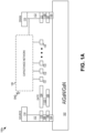
- FIG. 1A illustrates a simplified schematic 100a of a device cross section including a capacitance network 140 according to an embodiment.
- the simplified schematic 100a depicts a semiconductor layer 102 which may comprise aluminum gallium nitride (AlGaN), gallium nitride (GaN), and/or a combination of both AlGaN and GaN.
- the simplified schematic 100a further depicts interconnect to a source, gate, and a drain.
- interconnect layers may be identified as ohmic contacts 104-105, a source field plate (SFP) 106, a drain field plate (DFP) 107, vias 108-109, a first metal layer 110 (i.e.
- the gate interconnect may include a gate field plate 120, a via 122, and a first metal layer 124 ( i.e., to the gate).
- a drift region may exist along and/or near the surface ( i.e., top) of semiconductor layer 102 between the gate (GATE) and the drain (DRAIN).
- field plates 131-134 can be fabricated using the first metal layer so that the field plates 131-134 are disposed above the drift region of semiconductor layer 102.
- the field plates 131-134 may advantageously be formed on the same metal layer (i.e., metal 1) as first metal layers 110-111, 124 so as to reduce process steps and/or cost.
- the capacitance network 140 may be electrically connected to the field plates 131-134, to ground (GND), and/or to the drain at one or more layer (e.g. , at via 113).
- GND ground
- the capacitance network 140 may be electrically connected to the field plates 131-134, to ground (GND), and/or to the drain at one or more layer (e.g. , at via 113).
- FIG. 1A shows four field plates 131-134, there may be greater or fewer than four field plates 131-134. For instance, there may be just one field plate 131.
- the capacitance network 140 may be an external network and/or an internal ( i.e. , integrated) network which may be provided to adjust field plate potentials (i.e., field plate voltages).
- field plate potentials i.e., field plate voltages.
- an electric field within the drift region of semiconductor layer 102 may be adjusted ( i.e., distributed) in a controlled manner. In this way, the electric field may be distributed to be substantially uniform.
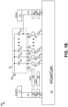
- FIG. 1B illustrates a schematic 100b of a device cross section including a capacitance network 140 according to an embodiment.
- Schematic 100b illustrates parasitic field plate capacitances C1-C4 and C11-C15.
- the parasitic field plate capacitances C1-C4 and C11-C15 may give rise to coupling such that field plates 131-134 are capacitively coupled.
- the capacitance network 140 may provide capacitors C21-C24 tailored to control and/or select field plate potentials ( i.e. , field plate voltages).
- the capacitors C21-C24 may be determined, at least in part, by simulation and/or by experiment so as to select the field plate potentials.
- FIG. 1C illustrates a schematic 100c of a device cross section including a capacitance network 140 according to an embodiment.
- the capacitance network 140 includes additional impedances R1-R6 electrically coupled between ground (GND) and the drain ( i.e. , to via 113).
- the impedances R1-R6 may be resistors, passive elements, and/or non-linear components ( e . g ., active field effect transistors) tailored to connect to the field plates 131-134.
- the impedances R1-R6 may advantageously provide a discharge feature allowing charge on the field plates 131-134 to be removed and/or controlled.
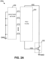
- FIG. 2A illustrates a schematic 200a of a device including a capacitance network 206 according to an embodiment.
- Schematic 200a includes a transistor 202 having a gate G, source S, and drain D; and as schematically illustrated, field plates 204 may be electrically coupled between the gate G and drain D.
- Schematic 200a also shows additional information relating to system voltages.
- the capacitance network 206 may be coupled to ground (GND) and to the field plates 204 to provide field plate potentials VFP1-VFP4.
- a drain to source voltage VDS may be applied at the drain D.
- a gate to source voltage VGS may be applied at the gate G; and the source S may be connected to ground (GND).
- FIG. 2B illustrates a schematic 200b of a device including a capacitance network 206 according to an embodiment.
- Field plates 204 include field plates 231-234 coupled with parasitic capacitances C30-C34.
- the capacitance network includes capacitors C35-C38 connected to the field plates 231-234, respectively.
- the values of capacitors C35-C38 may be selected so as to control ( i.e. , to select) the field plate potentials VFP1-VFP4; and by selecting the field plate potentials VFP1-VFP4, one may control an electric field along a drift region of transistor 202.
- the drift region of transistor 202 may be between the gate G and drain D; and there may be greater or fewer than four field plates 231-234. Accordingly, there may also be greater or fewer than four capacitors C35-C38.
- FIG. 2C illustrates a schematic 200c of a device including a capacitance network 206 according to an embodiment.
- Schematic 200c illustrates an embodiment including a discharge network 207.
- the discharge network 207 may also connect to field plates 204.
- FIG. 2D illustrates a schematic of a device 200d including a capacitance network 206 according to an embodiment.
- the discharge network 207 may include impedances Z1-Z5 electrically coupled between the drain D and the gate G.
- the impedances are also electrically coupled to the field plates 231-234 so as to provide a discharge feature.
- the impedances Z1-Z5 may be implemented by active devices ( e . g ., field effect transistors).
- the impedances Z1-Z5 may be implemented by resistors and/or by passive components.
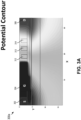
- FIG. 3A illustrates a device cross section 300a including potential contours according to an embodiment.
- the device cross section 300a may be that of a HEMT device including a source (S) 302, a gate (G) 304, and a drain (D) 306.
- the device cross section 300a also shows field plates 312-314 located between the gate 304 and drain 306 along an "X" axis.
- the potential contours may be derived from a simulation of the device cross section 300a.
- FIG. 3B illustrates a device cross section 300b including potential contours according to an embodiment.
- the potential contours are illustrated with lines and may also be derived using a device simulator.
- FIG. 3C illustrates a device cross section 300c including potential contours according to an embodiment.
- Device cross section 300c shows additional details relating to device materials and drift region. For instance, device cross section 300c shows a high voltage region 320 corresponding to where the field plates 312-314 are formed over a drift region ( i.e., a high voltage region).
- the field plates 312-314 may also labelled as field plates f1-f3.
- the device cross section 300c also delineates a GaN buffer layer 352 and an aluminum oxide (Al2O3) layer 354.
- simulation values of electrostatic potential (V) may be illustrated according to a color coded key ( e . g ., with values ranging between 1.0560 and 1,202.9 volts).
- FIG. 3C may correspond with a simulated potential contour for a 1200V device with three capacitively coupled field plates 312-314 (f1-f3). Assigning an adjusting external capacitance to each field plate, as means to emulate capacitance network, the device of FIG. 3C may be shown to support 1200V with a uniform 2DEG electric field in the extended HV region (see, e.g. , FIG. 4C ).
- FIG. 4A illustrates plots 402, 404 of potential and electric field as a function of distance along a drift region according to an embodiment.
- the embodiment may correspond with the simulation results of device cross sections 300a-c.
- plot 402 may correspond with potential and plot 404 may correspond with electric field.
- plot 404 is substantially uniform so as to improve plot 402 as a function of distance. In this way the maximum value of potential (i.e. , plot 402) reaches approximately 1200 volts (V).
- FIG. 4B illustrates plots 402, 404 of potential and electric field as a function of distance along a drift region according to an embodiment.
- FIG. 4B further delineates the location of the high voltage region 420 corresponding with the high voltage region 320.
- electric field is substantially uniform within the high voltage region 420 ( e . g ., within the drift region).
- FIG. 4C illustrates plots 402, 404 of potential and electric field as a function of distance along a drift region according to an embodiment.
- FIG. 4C can be similar to FIG. 4B except it includes additional labels showing the locations of the field plates 312-314 (f1-f3).
- plot 404 corresponding to potential, shows plateaus 431-433 corresponding to the locations of field plates 312-314 (f1-f3).
- the device may support 1200 volts with uniform 2DEG electric field in the extended high voltage (HV) region 420.
- a uniform electrical field in the two-dimensional electron gate (2DEG) region can advantageously provide a stable dynamic on-resistance (Rdson) in a GaN device.
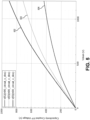
- FIG. 5 illustrates plots corresponding to field plate potentials 502-504 as a function of drain voltage according to an embodiment.
- the embodiment may also correspond with the simulation results of device cross sections 300a-c.
- the field plate potentials 502-504 are provided as a function of drain voltage Vdrain and may show how a coupling ratio of each field plate 312-314 ( e . g ., field plates f1-f3) can be calculated by a ratio of a field plate potential to drain voltage.
- FIG. 6 illustrates a top layout view 600 of a device according to an embodiment.
- the top layout view 600 shows an active region 610 with stripes oriented parallel to a direction YP.
- transistors and/or semiconductor devices may be fabricated to have active regions wherein current, voltage, and/or power may be actively controlled; additionally there may be interconnect layers including pad layers adjacent to the active region(s).
- the top layout view 600 also shows where interconnect ( e . g ., metallization and/or pad layers) may be located to connect to a drain D and a source S.
- pads 601-603 may be drain pads 601-603 allowing connection ( i .
- pad 608 may be a source pad 608 allowing connection ( i . e ., electrical connection) to source stripes and/or segments within the active region 610.
- pad 607 may be a gate pad 607 allowing connection ( i.e. , electrical connection) to gate regions within the active region 610.
- a capacitance network (e . g ., capacitance network 140 and/or capacitance network 206) may be placed outside of the active region 610.
- capacitance network 606 may be placed outside of the active region 610 near the drain pad 602.
- field plates e.g. , field plates 131-134, field plates 204, and/or field plates 312-314) may be placed inside the active region 610.
- field plates such as field plates 312-314, may be positioned parallel to the direction YP and within ( i.e. , inside) the active region 610.
- FIG. 6 shows capacitance network 606 as being placed near the drain pad 602, other placements are possible.
- the capacitance network 606 may be placed near or within the source pad 608.
- a device may use a layout with multiple capacitance networks and/or integrated capacitance networks as described below with regards to FIG. 10A and FIG. 11A .
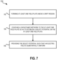
- FIG. 7 illustrates a conceptual flow diagram 700 for distributing an electric field in a drift region ( e.g. , a high voltage region 320 and/or 420) according to an embodiment.
- Step 702 may correspond with forming at least one field plate (e.g. , any one of field plates 131-134, 231-234, 312-314, and/or f1-f3) above the drift region.
- Step 704 may correspond with coupling a capacitance network ( e . g ., capacitance network 140, 206) to the at least one field plate so as to establish a select potential ( e . g ., any one of field plate potentials VFP1-VFP4) on the at least one field plate.
- Step 706 may correspond with providing the select potential such that an electric field (see, e.g., plot 404 of electric field) is substantially uniform (see, e.g. , plot 404 within high voltage region 420).
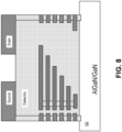
- FIG. 8 illustrates a traditional field plate design for a high voltage lateral gallium nitride device
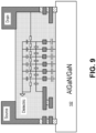
- FIG. 9 illustrates a lateral gallium nitride device cross-section and electrical schematic according to the teachings herein.
- FIG. 9 may further illustrate parasitic capacitance, resistor static discharge network elements, and a capacitance network for coupling ratio establishment.
- a capacitance network can be realized by a metal-insulator-metal (MIM) structure; a MIM structure can be inherent to a GaN process.
- the MIM structure can be realized through vertical metal plates and/or adjacent metal comb plates.
- FIG. 10A illustrates a top layout view 1000 of a device according to an embodiment. Similar to top layout view 600, the top layout view 1000 shows an active region 1020 with stripes oriented parallel to the direction YP. Additionally, the top layout view 1000 also shows where interconnect (e . g ., metallization and/or pad layers) may be located to connect to the drain D and the source S. For instance, pads 1004-1006 may be drain pads 1004-1006 allowing connection ( i . e ., electrical connection) to drain stripes and/or segments within the active region 1020; and pad 1024 may be a source pad 1024 allowing connection ( i . e ., electrical connection) to source stripes and/or segments within the active region 1020. Additionally, pad 1023 may be a gate pad 1023 allowing connection ( i.e., electrical connection) to gate regions within the active region 1020.
- interconnect e . g ., metallization and/or pad layers
- a capacitance network (e . g ., capacitance network 140 and/or capacitance network 206) may include a capacitor 1021 and a capacitor 1022 placed outside of the active region 1020.
- Field plates such as field plates 312-314, may be positioned parallel to the direction YP and within ( i . e ., inside) the active region 1020.
- FIG. 10B illustrates a top layout view of the stripe region 1025 according to the embodiment of FIG. 10A and shows a field plate pattern 1050 and field plate pattern 1051.
- Field plate pattern 1050 may electrically couple to capacitor 1021 (or capacitor 1022); and field plate pattern 1051 may electrically couple to capacitor 1022 (or capacitor 1021).
- capacitors 1021 and 1022 may have capacitance values in the range of one to ten picoFarads (pF); for instance, capacitor 1021 may have a value of 5.4pF and capacitor 1022 may have a value of 7.6pF.
- FIG. 11A illustrates a top layout view 1100 of a device according to an embodiment. Similar to top layout view 600 and top layout view 1000, the top layout view 1100 shows an active region 1120 with stripes oriented parallel to the direction YP. However, unlike the embodiments shown in top layout views 600 and 1000, the device of top layout view 1100 realizes a capacitor network ( e . g ., capacitance network 140 and/or capacitance network 206) using an embedded capacitor distributed within the active region 1120.
- a capacitor network e . g ., capacitance network 140 and/or capacitance network 206
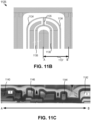
- FIG. 11B illustrates a top layout view and FIG. 11C illustrates a cross sectional view of the stripe region 1125 according to the embodiment of FIG. 11A .
- FIG. 11B illustrates a field plate pattern 1134 is electrically coupled with an embedded capacitor pattern 1136 by an interconnect link 1135.
- a cross section line 1137 delineated between points A (source S) and B (drain D) of top layout view may correspond with the cross sectional view of FIG. 11C .
- Point A may align (and be electrically coupled) with source interconnect 1140; and point B may align (and be electrically coupled) with drain interconnect 1142.
- the embedded capacitor pattern 1136 may be electrically coupled with embedded capacitor 1146; and the field plate pattern 1134 may be electrically coupled with field plate 1144.
- a problem solved by capacitance networks for enhancing high voltage operation of high electron mobility transistors may include enabling high voltage operation of a lateral gallium nitride (GaN) device without adding process complexity and cost.
- Ideal ( i . e ., traditional) field plate design for a lateral HV device may have a nearly square e-field distribution along drift region. This may be achieved by increasing level of field plates with increasing dielectric thickness as breakdown voltage increases (see, e.g., FIG. 8 ); but this adds process cost and complexity.
- the teachings herein may be applicable to a lateral GaN device with a number of capacitively coupled field plates; and the field plates may preferably built on the same metal layer for lower cost, whereby the potential on each field plate may be pre-determined through a capacitance network, resulting in a uniform e-field distribution along drift region at maximum operating voltage.
- a function of capacitance networks may be to establish a desired potential on each capacitively coupled field plate, by means of pre-determined capacitance in combination with parasitic capacitance to result in the right (e.g. , the ideal or substantially ideal) coupling ratio.
Landscapes
- Junction Field-Effect Transistors (AREA)
- Insulated Gate Type Field-Effect Transistor (AREA)
- Electrodes Of Semiconductors (AREA)
- Engineering & Computer Science (AREA)
- Power Engineering (AREA)
Abstract
Description
- The present invention relates to capacitance networks for enhancing high voltage operation of a high electron mobility transistor (HEMT) and more particularly to a lateral gallium nitride (GaN) HEMT having field plates coupled via capacitance networks.
- Gallium nitride (GaN) and other wide band-gap nitride III based direct transitional semiconductor materials exhibit high break-down electric fields and avail high current densities. In this regard GaN based semiconductor devices are actively researched as an alternative to silicon based semiconductor devices in power and high frequency applications. For instance, a GaN HEMT may provide lower specific on resistance with higher breakdown voltage relative to a silicon power field effect transistor of commensurate area.
- Power field effect transistors (FETs) can be enhancement mode or depletion mode. An enhancement mode device may refer to a transistor (e.g., a field effect transistor) which blocks current (i.e., which is off) when there is no applied gate bias (i.e., when the gate to source bias is zero). In contrast, a depletion mode device may refer to a transistor which allows current (i.e., which is on) when the gate to source bias is zero.
- Non-limiting and non-exhaustive embodiments of capacitance networks for enhancing high voltage operation of high electron mobility transistors (HEMTs) are described with reference to the following figures, wherein like reference numerals refer to like parts throughout the various views unless otherwise specified.
-
FIG. 1A illustrates a simplified schematic of a device cross section including a capacitance network according to an embodiment. -
FIG. 1B illustrates a schematic of a device cross section including a capacitance network according to an embodiment. -
FIG. 1C illustrates a schematic of a device cross section including a capacitance network according to an embodiment. -
FIG. 2A illustrates a schematic of a device including a capacitance network according to an embodiment. -
FIG. 2B illustrates a schematic of a device including a capacitance network according to an embodiment. -
FIG. 2C illustrates a schematic of a device including a capacitance network according to an embodiment. -
FIG. 2D illustrates a schematic of a device including a capacitance network according to an embodiment. -
FIG. 3A illustrates a device cross section including potential contours according to an embodiment. -
FIG. 3B illustrates a device cross section including potential contours according to an embodiment. -
FIG. 3C illustrates a device cross section including potential contours according to an embodiment. -
FIG. 4A illustrates plots of electric field and potential as a function of distance along a drift region according to an embodiment. -
FIG. 4B illustrates plots of electric field and potential as a function of distance along a drift region according to an embodiment. -
FIG. 4C illustrates plots of electric field and potential as a function of distance along a drift region according to an embodiment. -
FIG. 5 illustrates plots corresponding to field plate potentials as a function of drain voltage according to an embodiment. -
FIG. 6 illustrates a top layout view of a device according to an embodiment. -
FIG. 7 illustrates a conceptual flow diagram for distributing an electric field in a drift region according to an embodiment. -
FIG. 8 illustrates a traditional field plate design for a high voltage lateral gallium nitride device. -
FIG. 9 illustrates a lateral gallium nitride device cross-section and electrical schematic according to the teachings herein. -
FIG. 10A illustrates a top layout view of a device according to an embodiment. -
FIG. 10B illustrates a top layout view of a stripe region according to the embodiment ofFIG. 10A . -
FIG. 11A illustrates a top layout view of a device according to an embodiment. -
FIG. 11B illustrates a top layout view of a stripe region according to the embodiment ofFIG. 11A . -
FIG. 11C illustrates a cross sectional view of the stripe region according to the embodiment ofFIG. 11A . - Corresponding reference characters indicate corresponding components throughout the several views of the drawings. Skilled artisans will appreciate that elements in the figures are illustrated for simplicity and clarity and have not necessarily been drawn to scale. For example, the dimensions of some of the elements and layers in the figures may be exaggerated relative to other elements to help to improve understanding of various embodiments of the teachings herein. Also, common but well-understood elements, layers, and/or process steps that are useful or necessary in a commercially feasible embodiment are often not depicted in order to facilitate a less obstructed view of these various embodiments of capacitance networks for enhancing high voltage operation of high electron mobility transistors.
- In the following description, numerous specific details are set forth in order to provide a thorough understanding of capacitance networks for enhancing high voltage operation of high electron mobility transistors. It will be apparent, however, to one having ordinary skill in the art that the specific detail need not be employed to practice the teachings herein. In other instances, well-known materials or methods have not been described in detail in order to avoid obscuring the present disclosure.
- Reference throughout this specification to "one embodiment", "an embodiment", "one example" or "an example" means that a particular feature, structure, method, process, and/or characteristic described in connection with the embodiment or example is included in at least one embodiment of capacitance networks for enhancing high voltage operation of high electron mobility transistors. Thus, appearances of the phrases "in one embodiment", "in an embodiment", "one example" or "an example" in various places throughout this specification are not necessarily all referring to the same embodiment or example. Furthermore, the particular features, structures, methods, processes and/or characteristics may be combined in any suitable combinations and/or subcombinations in one or more embodiments or examples. In addition, it is appreciated that the figures provided herewith are for explanation purposes to persons ordinarily skilled in the art and that the drawings are not necessarily drawn to scale.
- In the context of the present application, when a transistor is in an "off-state" or "off' the transistor blocks current and/or does not substantially conduct current. Conversely, when a transistor is in an "on-state" or "on" the transistor is able to substantially conduct current. By way of example, in one embodiment, a high-voltage transistor comprises an N-channel metal-oxide-semiconductor (NMOS) field-effect transistor (FET) with the high-voltage being supported between the first terminal, a drain, and the second terminal, a source. In some embodiments an integrated controller circuit may be used to drive a power switch when regulating energy provided to a load. Also, for purposes of this disclosure, "ground" or "ground potential" refers to a reference voltage or potential against which all other voltages or potentials of an electronic circuit or Integrated circuit (IC) are defined or measured.
- As described above, a HEMT and/or a GaN HEMT may provide lower specific on resistance with higher breakdown voltage relative to a silicon power field effect transistor of commensurate area. It has been found, however, that breakdown voltage of HEMTs and/or GaN HEMTs may be limited by non-uniform electric fields in a drift region. Thus, it may be desirable to find ways to distribute an electric field in the drift region so that it becomes uniform and/or substantially uniform.
- Traditional approaches to distributing an electric field include using field plates. However, a traditional field plate design for a high voltage HEMT (e.g., a lateral high voltage HEMT) may be limited to providing a square electric field distribution along the drift region; moreover, the traditional field plate design may necessitate a thick dielectric to support a high breakdown voltage. This, in turn, may increase process cost and complexity. Accordingly, it may also be desirable to find ways to distribute an electric field without increasing process cost and complexity.
- Capacitance networks for enhancing high voltage operation of high electron mobility transistors (HEMTs) are presented herein. A capacitance network, integrated and/or external, may be provided with a fixed number of capacitively coupled field plates to distribute the electric field in the drift region. The capacitively coupled field plates may advantageously be fabricated on the same metal layer to lower cost; and the capacitance network may be provided to control field plate potentials. The potentials on each field plate may be pre-determined through the capacitance network, resulting in a uniform, and/or a substantially uniform electric field distribution along the drift region.
-
FIG. 1A illustrates a simplified schematic 100a of a device cross section including acapacitance network 140 according to an embodiment. The simplified schematic 100a depicts asemiconductor layer 102 which may comprise aluminum gallium nitride (AlGaN), gallium nitride (GaN), and/or a combination of both AlGaN and GaN. The simplified schematic 100a further depicts interconnect to a source, gate, and a drain. In one embodiment, interconnect layers may be identified as ohmic contacts 104-105, a source field plate (SFP) 106, a drain field plate (DFP) 107, vias 108-109, a first metal layer 110 (i.e., to the source), a first metal layer 111 (i.e., to the drain), vias 112-113, a second metal layer 114 (i.e., to the source), and a second metal 115 (i.e., to the drain). Additionally, the gate interconnect may include agate field plate 120, a via 122, and a first metal layer 124 (i.e., to the gate). - A drift region may exist along and/or near the surface (i.e., top) of
semiconductor layer 102 between the gate (GATE) and the drain (DRAIN). Along the drift region, field plates 131-134 can be fabricated using the first metal layer so that the field plates 131-134 are disposed above the drift region ofsemiconductor layer 102. The field plates 131-134 may advantageously be formed on the same metal layer (i.e., metal 1) as first metal layers 110-111, 124 so as to reduce process steps and/or cost. - The
capacitance network 140 may be electrically connected to the field plates 131-134, to ground (GND), and/or to the drain at one or more layer (e.g., at via 113). Although the embodiment ofFIG. 1A shows four field plates 131-134, there may be greater or fewer than four field plates 131-134. For instance, there may be just onefield plate 131. - The
capacitance network 140 may be an external network and/or an internal (i.e., integrated) network which may be provided to adjust field plate potentials (i.e., field plate voltages). By adjusting the field plate potentials to known (i.e., selected) values, an electric field within the drift region ofsemiconductor layer 102 may be adjusted (i.e., distributed) in a controlled manner. In this way, the electric field may be distributed to be substantially uniform. -
FIG. 1B illustrates a schematic 100b of a device cross section including acapacitance network 140 according to an embodiment.Schematic 100b illustrates parasitic field plate capacitances C1-C4 and C11-C15. The parasitic field plate capacitances C1-C4 and C11-C15 may give rise to coupling such that field plates 131-134 are capacitively coupled. Thecapacitance network 140 may provide capacitors C21-C24 tailored to control and/or select field plate potentials (i.e., field plate voltages). The capacitors C21-C24 may be determined, at least in part, by simulation and/or by experiment so as to select the field plate potentials. -
FIG. 1C illustrates a schematic 100c of a device cross section including acapacitance network 140 according to an embodiment. Thecapacitance network 140 includes additional impedances R1-R6 electrically coupled between ground (GND) and the drain (i.e., to via 113). The impedances R1-R6 may be resistors, passive elements, and/or non-linear components (e.g., active field effect transistors) tailored to connect to the field plates 131-134. In some embodiments the impedances R1-R6 may advantageously provide a discharge feature allowing charge on the field plates 131-134 to be removed and/or controlled. -
FIG. 2A illustrates a schematic 200a of a device including acapacitance network 206 according to an embodiment.Schematic 200a includes atransistor 202 having a gate G, source S, and drain D; and as schematically illustrated,field plates 204 may be electrically coupled between the gate G and drainD. Schematic 200a also shows additional information relating to system voltages. For instance, thecapacitance network 206 may be coupled to ground (GND) and to thefield plates 204 to provide field plate potentials VFP1-VFP4. In addition, a drain to source voltage VDS may be applied at the drain D. Also, a gate to source voltage VGS may be applied at the gate G; and the source S may be connected to ground (GND). -
FIG. 2B illustrates a schematic 200b of a device including acapacitance network 206 according to an embodiment.Field plates 204 include field plates 231-234 coupled with parasitic capacitances C30-C34. The capacitance network includes capacitors C35-C38 connected to the field plates 231-234, respectively. The values of capacitors C35-C38 may be selected so as to control (i.e., to select) the field plate potentials VFP1-VFP4; and by selecting the field plate potentials VFP1-VFP4, one may control an electric field along a drift region oftransistor 202. The drift region oftransistor 202 may be between the gate G and drain D; and there may be greater or fewer than four field plates 231-234. Accordingly, there may also be greater or fewer than four capacitors C35-C38. -
FIG. 2C illustrates a schematic 200c of a device including acapacitance network 206 according to an embodiment.Schematic 200c illustrates an embodiment including adischarge network 207. Thedischarge network 207 may also connect to fieldplates 204. -
FIG. 2D illustrates a schematic of adevice 200d including acapacitance network 206 according to an embodiment. As illustrated, thedischarge network 207 may include impedances Z1-Z5 electrically coupled between the drain D and the gate G. The impedances are also electrically coupled to the field plates 231-234 so as to provide a discharge feature. In some embodiments the impedances Z1-Z5 may be implemented by active devices (e.g., field effect transistors). In other embodiments the impedances Z1-Z5 may be implemented by resistors and/or by passive components. -
FIG. 3A illustrates adevice cross section 300a including potential contours according to an embodiment. Thedevice cross section 300a may be that of a HEMT device including a source (S) 302, a gate (G) 304, and a drain (D) 306. Thedevice cross section 300a also shows field plates 312-314 located between thegate 304 and drain 306 along an "X" axis. The potential contours may be derived from a simulation of thedevice cross section 300a. -
FIG. 3B illustrates adevice cross section 300b including potential contours according to an embodiment. The potential contours are illustrated with lines and may also be derived using a device simulator. -
FIG. 3C illustrates adevice cross section 300c including potential contours according to an embodiment.Device cross section 300c shows additional details relating to device materials and drift region. For instance,device cross section 300c shows ahigh voltage region 320 corresponding to where the field plates 312-314 are formed over a drift region (i.e., a high voltage region). The field plates 312-314 may also labelled as field plates f1-f3. - The
device cross section 300c also delineates aGaN buffer layer 352 and an aluminum oxide (Al2O3)layer 354. Indevice cross section 300c, simulation values of electrostatic potential (V) may be illustrated according to a color coded key (e.g., with values ranging between 1.0560 and 1,202.9 volts). -
FIG. 3C may correspond with a simulated potential contour for a 1200V device with three capacitively coupled field plates 312-314 (f1-f3). Assigning an adjusting external capacitance to each field plate, as means to emulate capacitance network, the device ofFIG. 3C may be shown to support 1200V with a uniform 2DEG electric field in the extended HV region (see, e.g.,FIG. 4C ). -
FIG. 4A illustratesplots device cross sections 300a-c. Additionally,plot 402 may correspond with potential andplot 404 may correspond with electric field. As illustrated, between about seventeen microns and thirty five microns,plot 404 is substantially uniform so as to improveplot 402 as a function of distance. In this way the maximum value of potential (i.e., plot 402) reaches approximately 1200 volts (V). -
FIG. 4B illustratesplots FIG. 4B further delineates the location of thehigh voltage region 420 corresponding with thehigh voltage region 320. As illustrated byplot 404, electric field is substantially uniform within the high voltage region 420 (e.g., within the drift region). -
FIG. 4C illustratesplots FIG. 4C can be similar toFIG. 4B except it includes additional labels showing the locations of the field plates 312-314 (f1-f3). For instance,plot 404, corresponding to potential, shows plateaus 431-433 corresponding to the locations of field plates 312-314 (f1-f3). - As discussed above, the device may support 1200 volts with uniform 2DEG electric field in the extended high voltage (HV)
region 420. A uniform electrical field in the two-dimensional electron gate (2DEG) region can advantageously provide a stable dynamic on-resistance (Rdson) in a GaN device. -
FIG. 5 illustrates plots corresponding to field plate potentials 502-504 as a function of drain voltage according to an embodiment. The embodiment may also correspond with the simulation results ofdevice cross sections 300a-c. The field plate potentials 502-504 are provided as a function of drain voltage Vdrain and may show how a coupling ratio of each field plate 312-314 (e.g., field plates f1-f3) can be calculated by a ratio of a field plate potential to drain voltage. -
FIG. 6 illustrates atop layout view 600 of a device according to an embodiment. Thetop layout view 600 shows anactive region 610 with stripes oriented parallel to a direction YP. As one of skill in the art may understand, transistors and/or semiconductor devices may be fabricated to have active regions wherein current, voltage, and/or power may be actively controlled; additionally there may be interconnect layers including pad layers adjacent to the active region(s). In this regard, thetop layout view 600 also shows where interconnect (e.g., metallization and/or pad layers) may be located to connect to a drain D and a source S. For instance, pads 601-603 may be drain pads 601-603 allowing connection (i.e., electrical connection) to drain stripes and/or segments within theactive region 610; andpad 608 may be asource pad 608 allowing connection (i.e., electrical connection) to source stripes and/or segments within theactive region 610. Additionally, pad 607 may be agate pad 607 allowing connection (i.e., electrical connection) to gate regions within theactive region 610. - In one embodiment a capacitance network (e.g.,
capacitance network 140 and/or capacitance network 206) may be placed outside of theactive region 610. For instance, as shown inFIG. 6 ,capacitance network 606 may be placed outside of theactive region 610 near thedrain pad 602. Additionally, field plates (e.g., field plates 131-134,field plates 204, and/or field plates 312-314) may be placed inside theactive region 610. For instance, field plates, such as field plates 312-314, may be positioned parallel to the direction YP and within (i.e., inside) theactive region 610. AlthoughFIG. 6 showscapacitance network 606 as being placed near thedrain pad 602, other placements are possible. For instance, thecapacitance network 606 may be placed near or within thesource pad 608. Alternatively, a device may use a layout with multiple capacitance networks and/or integrated capacitance networks as described below with regards toFIG. 10A andFIG. 11A . -
FIG. 7 illustrates a conceptual flow diagram 700 for distributing an electric field in a drift region (e.g., ahigh voltage region 320 and/or 420) according to an embodiment. Step 702 may correspond with forming at least one field plate (e.g., any one of field plates 131-134, 231-234, 312-314, and/or f1-f3) above the drift region. Step 704 may correspond with coupling a capacitance network (e.g.,capacitance network 140, 206) to the at least one field plate so as to establish a select potential (e.g., any one of field plate potentials VFP1-VFP4) on the at least one field plate. Step 706 may correspond with providing the select potential such that an electric field (see, e.g.,plot 404 of electric field) is substantially uniform (see, e.g.,plot 404 within high voltage region 420). -
FIG. 8 illustrates a traditional field plate design for a high voltage lateral gallium nitride device; andFIG. 9 illustrates a lateral gallium nitride device cross-section and electrical schematic according to the teachings herein.FIG. 9 may further illustrate parasitic capacitance, resistor static discharge network elements, and a capacitance network for coupling ratio establishment. A capacitance network can be realized by a metal-insulator-metal (MIM) structure; a MIM structure can be inherent to a GaN process. The MIM structure can be realized through vertical metal plates and/or adjacent metal comb plates. -
FIG. 10A illustrates atop layout view 1000 of a device according to an embodiment. Similar totop layout view 600, thetop layout view 1000 shows an active region 1020 with stripes oriented parallel to the direction YP. Additionally, thetop layout view 1000 also shows where interconnect (e.g., metallization and/or pad layers) may be located to connect to the drain D and the source S. For instance, pads 1004-1006 may be drain pads 1004-1006 allowing connection (i.e., electrical connection) to drain stripes and/or segments within the active region 1020; andpad 1024 may be asource pad 1024 allowing connection (i.e., electrical connection) to source stripes and/or segments within the active region 1020. Additionally,pad 1023 may be agate pad 1023 allowing connection (i.e., electrical connection) to gate regions within the active region 1020. - In the embodiment of top layout view 1000 a capacitance network (e.g.,
capacitance network 140 and/or capacitance network 206) may include acapacitor 1021 and acapacitor 1022 placed outside of the active region 1020. Field plates, such as field plates 312-314, may be positioned parallel to the direction YP and within (i.e., inside) the active region 1020. - For instance,
FIG. 10B illustrates a top layout view of thestripe region 1025 according to the embodiment ofFIG. 10A and shows afield plate pattern 1050 andfield plate pattern 1051.Field plate pattern 1050 may electrically couple to capacitor 1021 (or capacitor 1022); andfield plate pattern 1051 may electrically couple to capacitor 1022 (or capacitor 1021). In one embodiment,capacitors capacitor 1021 may have a value of 5.4pF andcapacitor 1022 may have a value of 7.6pF. -
FIG. 11A illustrates atop layout view 1100 of a device according to an embodiment. Similar totop layout view 600 andtop layout view 1000, thetop layout view 1100 shows anactive region 1120 with stripes oriented parallel to the direction YP. However, unlike the embodiments shown intop layout views top layout view 1100 realizes a capacitor network (e.g.,capacitance network 140 and/or capacitance network 206) using an embedded capacitor distributed within theactive region 1120. - For instance,
FIG. 11B illustrates a top layout view andFIG. 11C illustrates a cross sectional view of thestripe region 1125 according to the embodiment ofFIG. 11A .FIG. 11B illustrates afield plate pattern 1134 is electrically coupled with an embeddedcapacitor pattern 1136 by aninterconnect link 1135. - A
cross section line 1137 delineated between points A (source S) and B (drain D) of top layout view may correspond with the cross sectional view ofFIG. 11C . Point A may align (and be electrically coupled) withsource interconnect 1140; and point B may align (and be electrically coupled) withdrain interconnect 1142. The embeddedcapacitor pattern 1136 may be electrically coupled with embeddedcapacitor 1146; and thefield plate pattern 1134 may be electrically coupled withfield plate 1144. - A problem solved by capacitance networks for enhancing high voltage operation of high electron mobility transistors (HEMTs) may include enabling high voltage operation of a lateral gallium nitride (GaN) device without adding process complexity and cost.
- Ideal (i.e., traditional) field plate design for a lateral HV device may have a nearly square e-field distribution along drift region. This may be achieved by increasing level of field plates with increasing dielectric thickness as breakdown voltage increases (see, e.g.,
FIG. 8 ); but this adds process cost and complexity. The teachings herein may be applicable to a lateral GaN device with a number of capacitively coupled field plates; and the field plates may preferably built on the same metal layer for lower cost, whereby the potential on each field plate may be pre-determined through a capacitance network, resulting in a uniform e-field distribution along drift region at maximum operating voltage. - Additionally, a function of capacitance networks may be to establish a desired potential on each capacitively coupled field plate, by means of pre-determined capacitance in combination with parasitic capacitance to result in the right (e.g., the ideal or substantially ideal) coupling ratio.
- The above description of illustrated examples of the present disclosure, including what is described in the Abstract, are not intended to be exhaustive or to be limitation to the precise forms disclosed. While specific embodiments of capacitance networks for enhancing high voltage operation of high electron mobility transistors are described herein for illustrative purposes, various equivalent modifications are possible without departing from the broader spirit and scope of the present disclosure. Indeed, it is appreciated that the specific example device cross sections are provided for explanation purposes and that other embodiments may also be employed in accordance with the teachings herein.
- Although the present invention is defined in the claims, it should be understood that the present invention can alternatively be defined in accordance with the following examples:
- Example 1. A high electron mobility transistor (HEMT) comprising: a drift region; at least one field plate disposed above the drift region, wherein the drift region is configured to support an electric field; and a capacitance network electrically coupled to the at least one field plate, wherein the capacitance network is configured to distribute the electric field.
- Example 2. The HEMT of example 1, wherein the HEMT is a lateral gallium nitride (GaN) semiconductor device.
- Example 3. The HEMT of any of the preceding examples, wherein the capacitance network is configured to uniformly distribute the electric field.
- Example 4. The HEMT of any of the preceding examples, wherein the capacitance network is configured to establish a select potential on the at least one field plate.
- Example 5. The HEMT of any of the preceding examples, wherein the select potential is selected to uniformly distribute the electric field.
- Example 6. The HEMT of any of the preceding examples, wherein the capacitance network comprises at least one impedance configured to discharge the at least one field plate.
- Example 7. A semiconductor device comprising: a drift region formed laterally between a gate and a drain, wherein the drift region is configured to support an electric field; a plurality of field plates disposed above the drift region, the plurality of field plates comprising: a first field plate configured to support a first potential; and a second field plate configured to support a second potential; and a capacitance network electrically coupled to the plurality of field plates, wherein the capacitance network is configured to establish the first potential and the second potential so as to distribute the electric field.
- Example 8. The semiconductor device of example 7, wherein the capacitance network is configured to establish the first potential and the second potential.
- Example 9. The semiconductor device of any one of examples 7-8, wherein the capacitance network comprises: a first capacitor electrically coupled to the first field plate; and a second capacitor electrically coupled to the second field plate.
- Example 10. The semiconductor device of any one of examples 7-9, wherein the capacitance network is an external capacitance network.
- Example 11. The semiconductor device of any one of examples 7-10, wherein the capacitance network comprises an embedded capacitor.
- Example 12. The semiconductor device of any one of examples 7-11, wherein the first capacitor is configured to establish the first potential and the second capacitor is configured to established the second potential.
- Example 13. The semiconductor device of any one of examples 7-12, wherein the first capacitor is electrically coupled between a direct current (DC) potential and the first field plate, and the second capacitor is electrically coupled between the DC potential and the second field plate.
- Example 14. The semiconductor device of any one of examples 7-13, wherein the capacitance network further comprises: a first impedance electrically coupled between the DC potential and the first field plate; and a second impedance electrically coupled between the drain and the second field plate.
- Example 15. The semiconductor device of any one examples 7-14, wherein the DC potential is ground.
- Example 16. The semiconductor device of any one of examples 7-15, wherein the plurality of field plates comprises a third field plate configured to support a third potential; wherein the capacitance network comprises: a third capacitor electrically coupled between the DC potential and the third field plate; a third impedance electrically coupled between the first field plate and the third field plate, and a fourth impedance electrically coupled between the third field plate and the second field plate.
- Example 17. The semiconductor device of any one of examples 7-16, wherein the capacitance network is configured to establish the first potential, the second potential, and the third potential so as to distribute the electric field.
- Example 18. The semiconductor device of any one of examples 7-17, wherein the electric field is substantially uniform.
- Example 19. The semiconductor device of any one of examples 7-18, wherein the electric field sustains a voltage of at least one-thousand two-hundred volts.
- Example 20. A method of distributing an electric field in a drift region of a high voltage semiconductor device comprising: forming at least one field plate above a drift region; coupling a capacitance network to the at least one field plate so as to establish a select potential on the at least one field plate; and providing the select potential such that the electric field is substantially uniform.
- Example 21. The method of example 20, wherein coupling the capacitance network to the at least one field plate comprises coupling a first capacitor to the at least one field plate.
- Example 22. The method of any one of examples 20-21, wherein coupling the capacitance network to the at least one field plate comprises coupling a static discharge impedance to the at least one field plate.
- Example 23. The method of any one of examples 20-22, wherein forming the at least one field plate above the drift region comprises forming the at least one field plate inside an active region.
- Example 24. The method of any one of examples 20-23, wherein coupling the capacitance network to the at least one field plate comprises forming the capacitance network outside the active region.
Claims (15)
- A method of forming a high electron mobility transistor "HEMT" semiconductor device (100) in which an electric field is distributed in a drift region of the semiconductor device (100) upon provision of a select potential, the method comprising:forming at least one field plate (131, 132, 133, 134) above a drift region;coupling a capacitance network to the at least one field plate, wherein the capacitance network is configured such that, upon provision of the select potential on the at least one field plate, the electric field in the drift region as substantially uniform.
- The method of claim 1, wherein coupling the capacitance network to the at least one field plate comprises coupling a first capacitor (C21, C24) to the at least one field plate (131, 132, 133, 134).
- The method of claim 2, wherein coupling the capacitance network to the at least one field plate comprises coupling a static discharge impedance to the at least one field plate (131, 132, 133, 134).
- The method of claim 1, wherein forming the at least one field plate above the drift region comprises forming the at least one field plate inside an active region.
- The method of claim 4, wherein coupling the capacitance network to the at least one field plate comprises forming the capacitance network outside the active region.
- The method of any preceding claim, comprising:forming the drift region laterally between a gate and a drain, wherein the drift region is configured to support an electric field;disposing a plurality of field plates (131, 132, 133, 134) above the drift region, the plurality of field plates comprising:wherein the capacitance network is configured to establish the first potential on the first field plate and the second potential on the second field plate so as to distribute the electric field in the drift region.a first field plate (131) configured to support a first potential; anda second field plate (134) configured to support a second potential; anda capacitance network (140) electrically coupled to the plurality of field plates,
- The method of claim 6, wherein the capacitance network comprisesa first capacitor (C21) electrically coupled to the first field plate and between the first field plate and a DC potential,a second capacitor (C24) electrically coupled to the second field plate and between the second field plate and the DC potential,a first impedance (R1) electrically coupled between the DC potential and the first field plate, anda second impedance (R6) electrically coupled between the drain and the second field plate.
- The method of claim 7, wherein the capacitance network comprises
one or more additional impedances (R2, R3, R4, R5) electrically coupled between the first field plate and the second field plate. - The method of claim 6, wherein the capacitance network is an external capacitance network.
- The method of claim 6, wherein the capacitance network comprises an embedded capacitor (1146).
- The method of claim 6, wherein the DC potential is ground.
- The method of claim 6,wherein the plurality of field plates comprises a third field plate (132, 133) configured to support a third potential;wherein the capacitance network comprises:
a third capacitor (C22, C23) electrically coupled between the DC potential and the third field plate; andwherein the one or morea third impedance (R2, R3) electrically coupled between the first field plate and the third field plate, anda fourth impedance (R3, R4, R5) electrically coupled between the third field plate and the second field plate. - The method of claim 12, wherein the capacitance network is configured to establish the first potential, the second potential, and the third potential so as to distribute the electric field.
- The method of claim 13, wherein the electric field sustains a voltage of at least one-thousand two-hundred volts.
- The method of any preceding claim, wherein the first impedance and the second impedance are field effect transistors.
Applications Claiming Priority (3)
| Application Number | Priority Date | Filing Date | Title |
|---|---|---|---|
| US201962873307P | 2019-07-12 | 2019-07-12 | |
| EP20740752.9A EP3997737B1 (en) | 2019-07-12 | 2020-06-24 | Capacitance networks for enhancing high voltage operation of a high electron mobility transistor and method therein |
| PCT/US2020/039344 WO2021011163A1 (en) | 2019-07-12 | 2020-06-24 | Capacitance networks for enhancing high voltage operation of a high electron mobility transistor and method therein |
Related Parent Applications (1)
| Application Number | Title | Priority Date | Filing Date |
|---|---|---|---|
| EP20740752.9A Division EP3997737B1 (en) | 2019-07-12 | 2020-06-24 | Capacitance networks for enhancing high voltage operation of a high electron mobility transistor and method therein |
Publications (2)
| Publication Number | Publication Date |
|---|---|
| EP4478422A2 true EP4478422A2 (en) | 2024-12-18 |
| EP4478422A3 EP4478422A3 (en) | 2025-03-12 |
Family
ID=71620514
Family Applications (2)
| Application Number | Title | Priority Date | Filing Date |
|---|---|---|---|
| EP24210232.5A Pending EP4478422A3 (en) | 2019-07-12 | 2020-06-24 | Capacitance networks for enhancing high voltage operation of a high electron mobility transistor and method therein |
| EP20740752.9A Active EP3997737B1 (en) | 2019-07-12 | 2020-06-24 | Capacitance networks for enhancing high voltage operation of a high electron mobility transistor and method therein |
Family Applications After (1)
| Application Number | Title | Priority Date | Filing Date |
|---|---|---|---|
| EP20740752.9A Active EP3997737B1 (en) | 2019-07-12 | 2020-06-24 | Capacitance networks for enhancing high voltage operation of a high electron mobility transistor and method therein |
Country Status (7)
| Country | Link |
|---|---|
| US (2) | US12446251B2 (en) |
| EP (2) | EP4478422A3 (en) |
| JP (2) | JP7456703B2 (en) |
| KR (2) | KR102785863B1 (en) |
| CN (1) | CN114127950A (en) |
| TW (2) | TWI827858B (en) |
| WO (1) | WO2021011163A1 (en) |
Families Citing this family (4)
| Publication number | Priority date | Publication date | Assignee | Title |
|---|---|---|---|---|
| US12166476B2 (en) * | 2022-12-14 | 2024-12-10 | Globalfoundries U.S. Inc. | High voltage device with linearizing field plate configuration |
| JP2024135948A (en) * | 2023-03-23 | 2024-10-04 | 株式会社東芝 | Semiconductor device and semiconductor module |
| US20240363697A1 (en) * | 2023-04-26 | 2024-10-31 | Taiwan Semiconductor Manufacturing Company, Ltd. | Quasi field-plate structure for semiconductor devices |
| TWI880292B (en) * | 2023-08-10 | 2025-04-11 | 新唐科技股份有限公司 | Semiconductor device |
Family Cites Families (18)
| Publication number | Priority date | Publication date | Assignee | Title |
|---|---|---|---|---|
| JP2006351753A (en) * | 2005-06-15 | 2006-12-28 | Mitsubishi Electric Corp | Field effect transistor |
| US8154079B2 (en) * | 2006-12-07 | 2012-04-10 | Kabushiki Kaisha Toshiba | Semiconductor device and fabrication method of the semiconductor device |
| US8502323B2 (en) * | 2007-08-03 | 2013-08-06 | The Hong Kong University Of Science And Technology | Reliable normally-off III-nitride active device structures, and related methods and systems |
| JP5609083B2 (en) | 2009-12-01 | 2014-10-22 | 日本電気株式会社 | SEMICONDUCTOR DEVICE, ELECTRONIC DEVICE, METHOD FOR MANUFACTURING AND USING SEMICONDUCTOR DEVICE |
| JP5594515B2 (en) | 2010-03-26 | 2014-09-24 | 日本電気株式会社 | Semiconductor device, electronic device, method for manufacturing semiconductor device, and method for operating semiconductor device |
| US8749016B2 (en) | 2010-10-06 | 2014-06-10 | Macronix International Co., Ltd. | High voltage MOS device and method for making the same |
| US20140001479A1 (en) * | 2012-06-29 | 2014-01-02 | Power Integrations, Inc. | Switching device with charge distribution structure |
| US9245879B2 (en) | 2012-06-29 | 2016-01-26 | Power Integrations, Inc. | Static discharge system |
| JP6091941B2 (en) | 2012-09-27 | 2017-03-08 | ルネサスエレクトロニクス株式会社 | Semiconductor device |
| JP2015050434A (en) | 2013-09-04 | 2015-03-16 | 古河電気工業株式会社 | Nitride semiconductor device |
| US9306014B1 (en) | 2013-12-27 | 2016-04-05 | Power Integrations, Inc. | High-electron-mobility transistors |
| US9761675B1 (en) * | 2015-01-08 | 2017-09-12 | National Technology & Engineering Solutions Of Sandia, Llc | Resistive field structures for semiconductor devices and uses therof |
| JP2016139718A (en) * | 2015-01-28 | 2016-08-04 | 株式会社東芝 | Semiconductor device |
| US9911817B2 (en) * | 2015-07-17 | 2018-03-06 | Cambridge Electronics, Inc. | Field-plate structures for semiconductor devices |
| EP3179515A1 (en) * | 2015-12-10 | 2017-06-14 | Nexperia B.V. | Semiconductor device and method of making a semiconductor device |
| JP7154015B2 (en) | 2017-03-03 | 2022-10-17 | パワー・インテグレーションズ・インコーポレーテッド | Switching device including charge distribution structure |
| JP2018196026A (en) | 2017-05-18 | 2018-12-06 | 株式会社豊田中央研究所 | Gate driving device |
| GB2564482B (en) * | 2017-07-14 | 2021-02-10 | Cambridge Entpr Ltd | A power semiconductor device with a double gate structure |
-
2020
- 2020-06-24 US US17/621,852 patent/US12446251B2/en active Active
- 2020-06-24 EP EP24210232.5A patent/EP4478422A3/en active Pending
- 2020-06-24 WO PCT/US2020/039344 patent/WO2021011163A1/en not_active Ceased
- 2020-06-24 JP JP2022500903A patent/JP7456703B2/en active Active
- 2020-06-24 EP EP20740752.9A patent/EP3997737B1/en active Active
- 2020-06-24 CN CN202080050614.4A patent/CN114127950A/en active Pending
- 2020-06-24 KR KR1020227001207A patent/KR102785863B1/en active Active
- 2020-06-24 KR KR1020257009116A patent/KR20250046345A/en active Pending
- 2020-07-06 TW TW109122790A patent/TWI827858B/en active
- 2020-07-06 TW TW112147566A patent/TWI884623B/en active
-
2024
- 2024-03-08 JP JP2024036329A patent/JP7713547B2/en active Active
-
2025
- 2025-09-16 US US19/330,567 patent/US20260013169A1/en active Pending
Also Published As
| Publication number | Publication date |
|---|---|
| JP2022550238A (en) | 2022-12-01 |
| EP4478422A3 (en) | 2025-03-12 |
| JP2024070863A (en) | 2024-05-23 |
| KR20220031619A (en) | 2022-03-11 |
| TW202111951A (en) | 2021-03-16 |
| KR20250046345A (en) | 2025-04-02 |
| US12446251B2 (en) | 2025-10-14 |
| TW202416532A (en) | 2024-04-16 |
| CN114127950A (en) | 2022-03-01 |
| TWI827858B (en) | 2024-01-01 |
| JP7456703B2 (en) | 2024-03-27 |
| EP3997737A1 (en) | 2022-05-18 |
| EP3997737B1 (en) | 2024-11-13 |
| JP7713547B2 (en) | 2025-07-25 |
| US20220262941A1 (en) | 2022-08-18 |
| TWI884623B (en) | 2025-05-21 |
| KR102785863B1 (en) | 2025-03-25 |
| WO2021011163A1 (en) | 2021-01-21 |
| US20260013169A1 (en) | 2026-01-08 |
Similar Documents
| Publication | Publication Date | Title |
|---|---|---|
| US20260013169A1 (en) | Capacitance networks for enhancing high voltage operation of a high electron mobility transistor and method therein | |
| KR100550148B1 (en) | Rf power unit with voltage controlled linearity | |
| US10181523B2 (en) | Transistor structure with improved unclamped inductive switching immunity | |
| US8785987B2 (en) | IGFET device having an RF capability | |
| US20070241368A1 (en) | Field effect transistor with independently biased gates | |
| KR102390898B1 (en) | High-electron-mobility transistors | |
| CN109509783A (en) | Semiconductor device | |
| KR20260014011A (en) | Distributed fet back-bias network | |
| EP4290773A1 (en) | Integrated resistor-transistor-capacitor snubber | |
| WO2016209934A1 (en) | High voltage device with multi-electrode control | |
| US20230155025A1 (en) | Semiconductor device | |
| CN109285830B (en) | semiconductor structure | |
| US9461037B2 (en) | Reduced generation of second harmonics of FETs | |
| US20130222953A1 (en) | High-voltage transistor, esd-protection circuit, and use of a high-voltage transistor in an esd-protection circuit | |
| CN113872581A (en) | RF switch | |
| TW201608829A (en) | Semiconductor device and cascade circuit | |
| CN111509030A (en) | Super junction MOSFET with integrated snubber circuit | |
| CN107395169A (en) | Switch | |
| US20120248533A1 (en) | Field plate and circuit therewith | |
| WO2016157813A1 (en) | Load driving apparatus | |
| US12610601B2 (en) | Field plate biasing of high electron mobility transistor |
Legal Events
| Date | Code | Title | Description |
|---|---|---|---|
| PUAI | Public reference made under article 153(3) epc to a published international application that has entered the european phase |
Free format text: ORIGINAL CODE: 0009012 |
|
| STAA | Information on the status of an ep patent application or granted ep patent |
Free format text: STATUS: REQUEST FOR EXAMINATION WAS MADE |
|
| 17P | Request for examination filed |
Effective date: 20241031 |
|
| AC | Divisional application: reference to earlier application |
Ref document number: 3997737 Country of ref document: EP Kind code of ref document: P |
|
| AK | Designated contracting states |
Kind code of ref document: A2 Designated state(s): AL AT BE BG CH CY CZ DE DK EE ES FI FR GB GR HR HU IE IS IT LI LT LU LV MC MK MT NL NO PL PT RO RS SE SI SK SM TR |
|
| REG | Reference to a national code |
Ref country code: DE Ref legal event code: R079 Free format text: PREVIOUS MAIN CLASS: H01L0029778000 Ipc: H10D0030470000 |
|
| PUAL | Search report despatched |
Free format text: ORIGINAL CODE: 0009013 |
|
| AK | Designated contracting states |
Kind code of ref document: A3 Designated state(s): AL AT BE BG CH CY CZ DE DK EE ES FI FR GB GR HR HU IE IS IT LI LT LU LV MC MK MT NL NO PL PT RO RS SE SI SK SM TR |
|
| RIC1 | Information provided on ipc code assigned before grant |
Ipc: H10D 84/80 20250101ALI20250205BHEP Ipc: H10D 64/00 20250101ALI20250205BHEP Ipc: H10D 62/85 20250101ALI20250205BHEP Ipc: H01L 23/64 20060101ALI20250205BHEP Ipc: H10D 30/47 20250101AFI20250205BHEP |
|
| STAA | Information on the status of an ep patent application or granted ep patent |
Free format text: STATUS: EXAMINATION IS IN PROGRESS |
|
| 17Q | First examination report despatched |
Effective date: 20260323 |