EP4478408A1 - Power semiconductor module and method of increasing pin alignment accuracy for power semiconductor modules - Google Patents
Power semiconductor module and method of increasing pin alignment accuracy for power semiconductor modules Download PDFInfo
- Publication number
- EP4478408A1 EP4478408A1 EP24177431.4A EP24177431A EP4478408A1 EP 4478408 A1 EP4478408 A1 EP 4478408A1 EP 24177431 A EP24177431 A EP 24177431A EP 4478408 A1 EP4478408 A1 EP 4478408A1
- Authority
- EP
- European Patent Office
- Prior art keywords
- power semiconductor
- semiconductor module
- positional offset
- pins
- exposed surface
- Prior art date
- Legal status (The legal status is an assumption and is not a legal conclusion. Google has not performed a legal analysis and makes no representation as to the accuracy of the status listed.)
- Pending
Links
Images







Classifications
-
- H—ELECTRICITY
- H10—SEMICONDUCTOR DEVICES; ELECTRIC SOLID-STATE DEVICES NOT OTHERWISE PROVIDED FOR
- H10P—GENERIC PROCESSES OR APPARATUS FOR THE MANUFACTURE OR TREATMENT OF DEVICES COVERED BY CLASS H10
- H10P72/00—Handling or holding of wafers, substrates or devices during manufacture or treatment thereof
- H10P72/50—Handling or holding of wafers, substrates or devices during manufacture or treatment thereof for positioning, orientation or alignment
-
- H—ELECTRICITY
- H10—SEMICONDUCTOR DEVICES; ELECTRIC SOLID-STATE DEVICES NOT OTHERWISE PROVIDED FOR
- H10W—GENERIC PACKAGES, INTERCONNECTIONS, CONNECTORS OR OTHER CONSTRUCTIONAL DETAILS OF DEVICES COVERED BY CLASS H10
- H10W46/00—Marks applied to devices, e.g. for alignment or identification
-
- H—ELECTRICITY
- H10—SEMICONDUCTOR DEVICES; ELECTRIC SOLID-STATE DEVICES NOT OTHERWISE PROVIDED FOR
- H10P—GENERIC PROCESSES OR APPARATUS FOR THE MANUFACTURE OR TREATMENT OF DEVICES COVERED BY CLASS H10
- H10P74/00—Testing or measuring during manufacture or treatment of wafers, substrates or devices
- H10P74/23—Testing or measuring during manufacture or treatment of wafers, substrates or devices characterised by multiple measurements, corrections, marking or sorting processes
-
- H—ELECTRICITY
- H10—SEMICONDUCTOR DEVICES; ELECTRIC SOLID-STATE DEVICES NOT OTHERWISE PROVIDED FOR
- H10W—GENERIC PACKAGES, INTERCONNECTIONS, CONNECTORS OR OTHER CONSTRUCTIONAL DETAILS OF DEVICES COVERED BY CLASS H10
- H10W72/00—Interconnections or connectors in packages
- H10W72/071—Connecting or disconnecting
-
- H—ELECTRICITY
- H10—SEMICONDUCTOR DEVICES; ELECTRIC SOLID-STATE DEVICES NOT OTHERWISE PROVIDED FOR
- H10W—GENERIC PACKAGES, INTERCONNECTIONS, CONNECTORS OR OTHER CONSTRUCTIONAL DETAILS OF DEVICES COVERED BY CLASS H10
- H10W76/00—Containers; Fillings or auxiliary members therefor; Seals
- H10W76/10—Containers or parts thereof
- H10W76/12—Containers or parts thereof characterised by their shape
- H10W76/15—Containers comprising an insulating or insulated base
-
- H—ELECTRICITY
- H10—SEMICONDUCTOR DEVICES; ELECTRIC SOLID-STATE DEVICES NOT OTHERWISE PROVIDED FOR
- H10W—GENERIC PACKAGES, INTERCONNECTIONS, CONNECTORS OR OTHER CONSTRUCTIONAL DETAILS OF DEVICES COVERED BY CLASS H10
- H10W90/00—Package configurations
- H10W90/701—Package configurations characterised by the relative positions of pads or connectors relative to package parts
-
- H—ELECTRICITY
- H10—SEMICONDUCTOR DEVICES; ELECTRIC SOLID-STATE DEVICES NOT OTHERWISE PROVIDED FOR
- H10W—GENERIC PACKAGES, INTERCONNECTIONS, CONNECTORS OR OTHER CONSTRUCTIONAL DETAILS OF DEVICES COVERED BY CLASS H10
- H10W46/00—Marks applied to devices, e.g. for alignment or identification
- H10W46/101—Marks applied to devices, e.g. for alignment or identification characterised by the type of information, e.g. logos or symbols
-
- H—ELECTRICITY
- H10—SEMICONDUCTOR DEVICES; ELECTRIC SOLID-STATE DEVICES NOT OTHERWISE PROVIDED FOR
- H10W—GENERIC PACKAGES, INTERCONNECTIONS, CONNECTORS OR OTHER CONSTRUCTIONAL DETAILS OF DEVICES COVERED BY CLASS H10
- H10W46/00—Marks applied to devices, e.g. for alignment or identification
- H10W46/101—Marks applied to devices, e.g. for alignment or identification characterised by the type of information, e.g. logos or symbols
- H10W46/106—Marks applied to devices, e.g. for alignment or identification characterised by the type of information, e.g. logos or symbols digital information, e.g. bar codes
-
- H—ELECTRICITY
- H10—SEMICONDUCTOR DEVICES; ELECTRIC SOLID-STATE DEVICES NOT OTHERWISE PROVIDED FOR
- H10W—GENERIC PACKAGES, INTERCONNECTIONS, CONNECTORS OR OTHER CONSTRUCTIONAL DETAILS OF DEVICES COVERED BY CLASS H10
- H10W46/00—Marks applied to devices, e.g. for alignment or identification
- H10W46/301—Marks applied to devices, e.g. for alignment or identification for alignment
-
- H—ELECTRICITY
- H10—SEMICONDUCTOR DEVICES; ELECTRIC SOLID-STATE DEVICES NOT OTHERWISE PROVIDED FOR
- H10W—GENERIC PACKAGES, INTERCONNECTIONS, CONNECTORS OR OTHER CONSTRUCTIONAL DETAILS OF DEVICES COVERED BY CLASS H10
- H10W46/00—Marks applied to devices, e.g. for alignment or identification
- H10W46/401—Marks applied to devices, e.g. for alignment or identification for identification or tracking
-
- H—ELECTRICITY
- H10—SEMICONDUCTOR DEVICES; ELECTRIC SOLID-STATE DEVICES NOT OTHERWISE PROVIDED FOR
- H10W—GENERIC PACKAGES, INTERCONNECTIONS, CONNECTORS OR OTHER CONSTRUCTIONAL DETAILS OF DEVICES COVERED BY CLASS H10
- H10W46/00—Marks applied to devices, e.g. for alignment or identification
- H10W46/601—Marks applied to devices, e.g. for alignment or identification for use after dicing
- H10W46/607—Located on parts of packages, e.g. on encapsulations or on package substrates
-
- H—ELECTRICITY
- H10—SEMICONDUCTOR DEVICES; ELECTRIC SOLID-STATE DEVICES NOT OTHERWISE PROVIDED FOR
- H10W—GENERIC PACKAGES, INTERCONNECTIONS, CONNECTORS OR OTHER CONSTRUCTIONAL DETAILS OF DEVICES COVERED BY CLASS H10
- H10W90/00—Package configurations
Definitions
- the present disclosure relates to a power semiconductor module, in particular to a positional offset encoded on a power semiconductor module.
- Power semiconductor modules typically have a current rating between 6A and 3600A (or higher) cover a power range from hundreds of watts to several megawatts, and have wide adoption across many applications such as general purpose drives, traction, servo-units, renewable energy applications like solar inverters or wind applications, hybrid electric and full electric vehicle applications, etc.
- the electrical connection interface for power semiconductor modules typically includes contact pins that provide an electrical interface between the power semiconductor dies housed in the electrically insulative enclosure of the module and a circuit board with additional electronic components.
- the method comprises: determining a positional deviation of each pin of the plurality of pins from a respective target position in a coordinate system; determining a positional offset for the power semiconductor module based on the positional deviations of the pins, the positional offset reducing overall misalignment between the plurality of pins and the target positions; and encoding the positional offset on an exposed surface of the power semiconductor module.
- the method comprises: deciphering a positional offset encoded on the exposed surface of the power semiconductor module, the positional offset reducing overall misalignment between the plurality of pins and target positions for the pins; securing the power semiconductor module by automated equipment; adjusting a pressing position of the automated equipment in relation to a circuit board, based on the deciphered positional offset; and after adjusting the pressing position, pressing the plurality of pins into respective openings in the circuit board via the automated equipment.
- the power semiconductor module comprises: a plurality of power semiconductor dies attached to a substrate; a housing secured to the substrate and enclosing the plurality of power semiconductor dies; a plurality of pins protruding from the housing; and a positional offset encoded on the exposed surface of the power semiconductor module, the positional offset reducing overall misalignment between the plurality of pins and target positions for the pins.
- a positional offset is encoded on an exposed surface of a power semiconductor module that reduces overall misalignment between the module pins and target positions for the pins.
- a method of increasing overall pin alignment accuracy for the power semiconductor module and a method of mounting the power semiconductor module to a circuit board and/or a heat sink are also described.
- the encoded positional offset can be used to adjust a pressing position of automated equipment in relation to a circuit board, to reduce overall misalignment between the module pins and corresponding openings (apertures) in a circuit board when the automated equipment presses the module pins into the board openings.
- the individual pin tip positions do not need to be optically scanned during the module mounting process. Instead, the encoded positional offset simply needs to be ascertained from the exposed surface of the power semiconductor module and deciphered to determine an optimal pressing position for the power semiconductor module.
- FIG. 1 illustrates an exploded view of a power semiconductor module 100.
- the power semiconductor module 100 may form part of a power electronics circuit for use in various power applications such as a DC/AC inverter, a DC/DC converter, an AC/DC converter, a DC/AC converter, an AC/AC converter, a multi-phase inverter, an H-bridge, motor drive, etc.
- the power semiconductor module 100 includes power semiconductor dies 102 attached to a substrate 104.
- An electrically insulative housing 106 is secured to the substrate 104 as indicated by the downward facing arrows in FIG. 1 , and encloses the power semiconductor dies 102.
- the housing 106 may be secured to the substrate 104 by an adhesive, plastic cement, etc.
- the power semiconductor dies 102 may be electrically contacted at the backside by the patterned metallization 110 of the substrate 104 and at the frontside by bond wires 112, metal clips (not shown), etc.
- the power semiconductor dies 102 may include power Si or SiC power MOSFET (metal-oxide-semiconductor field-effect transistor) dies, HEMT (high-electron mobility transistor) dies, IGBT (insulated-gate bipolar transistor) dies, JFET (junction filed-effect transistor) dies, power diode dies, etc.
- Some or all of the power semiconductor dies 102 may be, e.g., vertical power transistor dies. For a vertical power transistor die, the primary current flow path is between the front and back sides of the die.
- the drain pad is typically disposed at the backside of the die, with the gate and source pads (and optionally one or more sense pads) at the frontside of the die.
- Additional types of semiconductor dies may be included in the power semiconductor module 100, e.g., such as one or more logic dies, controller dies, gate driver dies, etc.
- the power semiconductor module 100 also includes pins 112 that protrude from the housing 106.
- the pins 112 are attached to the substrate 104 and/or another structure such as a metallic lead frame or clip frame enclosed by the housing 106, and protrude through a first side 114 of the housing 106 to form an electrical connection interface outside the housing 106.
- the pins 112 extend through openings 118 in the first side 114 of the housing 106.
- the pins 112 are press-fit pins
- the term 'press-fit' as used herein refers to a pin geometry that enables plastic and/or elastic deformation in an upper region of the pins 112 when the pins 112 are inserted into corresponding openings of a circuit board (not shown in FIG. 1 ) such as a PCB (printed circuit board) or other type of component, providing effective contact points within the contact zone.
- the contact radius increases due to the contact pressure since the macroscopic contact force concentrates on a microscopic contact area. Accordingly, the pin face and the metallized face of the opening of the circuit board merge, i.e., are cold welded.
- Such a press-fit connection increases the effective contact zone and may provide a gas-tight contact zone that is robust against corrosive environments.
- the pins 112 include a tip part 118 configured to guide the press-fit pin 112 into a respective opening of a circuit board.
- a deformable part 120 adjoins the tip part 118 and is configured to plastically and/or elastically deform upon insertion into the corresponding circuit board opening.
- An elongate part 122 adjoins the deformable part 120 and has a length that may be chosen to accommodate the thickness (height) of the module housing 106 through which the press-fit pin 112 protrudes.
- a base part 124 adjoins the elongate part 122 and may be the widest part of the press-fit pin 112 to accommodate a force applied to the base part 124 for pressing the pin 112 into a sleeve 126 attached to the substrate 104.
- An anchoring part (out-of-view in FIG. 1 ) adjoins the base part 124 and is received by the corresponding sleeve 126.
- Part of a metallic lead frame or clip frame included (not shown in FIG. 1 ) in the power semiconductor module 100 may protrude through one or more side faces of the housing 106 to form a power terminal which may provide a reference voltage to the power semiconductor module 100 or carry current to or from the power semiconductor module 100.
- the electrical connection interface formed by the pins 112 provides an electrical interface to the power semiconductor dies 102 enclosed by the housing 106.
- the pins 112 may have a pin geometry that enables plastic and/or elastic deformation of a deformable part 120 of the pins 112 upon insertion of the tip-end 118 of the pins 112 into corresponding openings of a circuit board.
- One or more metallic tabs 128 or similar anchoring structures may protrude from the housing 106 to provide an anchoring point for securing the power semiconductor module 100 to a heat sink (not shown in FIG. 1 ).
- FIGS. 2A and 2B illustrate two different pin alignment scenarios for the power semiconductor module 100.
- a circuit board 200 such as a PCB
- all module pins 112 should be received by respective (apertures) openings 202 in the circuit board 200.
- the vertical centerline 204 of the illustrated pin tip 118 is offset from the vertical centerline 206 of the corresponding circuit board opening 202 but by an acceptable amount ⁇ x1. Accordingly, the pin 112 in FIG. 2A is properly received by the corresponding circuit board opening 202 during press fitting of the power semiconductor module 100.
- the vertical centerline 204 of the illustrated pin tip 118 also is offset from the vertical centerline 206 of the corresponding circuit board opening 202 by an amount ⁇ x2 that is outside the permitted alignment tolerance. Accordingly, the pin 112 in FIG. 2B is not received by the corresponding circuit board opening 202 during press fitting of the power semiconductor module 100 which results in damage to the pin 112 and/or circuit board 200.
- a positional offset is encoded on an exposed surface of the power semiconductor module 100.
- the positional offset reduces the overall misalignment between the pins 112 and target positions for the pins 112.
- the encoded positional offset can be used to adjust a pressing position of automated equipment (not shown in FIGS. 2A and 2B ) in relation to the circuit board 200, to reduce overall misalignment between the module pins 112 and corresponding openings 202 in the circuit board 200 when the automated equipment presses the module pins 112 into the board openings 202 as indicated by the upward facing arrows in FIGS. 2A and 2B .
- FIG. 1 illustrates different embodiments of the positional offset encoded on an exposed surface of the power semiconductor module 100.
- the positional offset may include one or more fiducial marks 130 indicative of the positional offset.
- Each fiducial mark 130 is decipherable by an imaging system and may be used as a point of reference for adjusting the position (X, Y and/or rotational) of the power semiconductor module 100 during module mounting to ensure pin alignment accuracy.
- the positional offset may include a barcode 132 indicative of the positional offset.
- the barcode 132 may be (linear) one-dimensional or (matrix) two-dimensional.
- the barcode 132 is decipherable by a barcode reader system and may be used to indicate a positional (X, Y and/or rotational) shift for the power semiconductor module 100 during module mounting to ensure pin alignment accuracy.
- the barcode 132 may relate the positional offset to a plurality of mounting regions 134 of the housing 106.
- the mounting regions 106 are configured to enable mounting of the housing 106 to a body such a circuit board, heat sink, etc.
- the mounting regions 106 may be used to locate the module housing during PCB installation (e.g., as shown in FIG. 16 ) and may also be used after PCB installation, e.g., to secure the PCB to the housing 106 with screws, for example.
- alignment instructions indicated by the positional offset may be encoded in the barcode 132 such that the barcode 132 relates the positional offset to the mounting regions 134 of the housing 106.
- the barcode 132 may instead relate the positional offset to other features already present on the housing 106, e.g., such as pegs or through holes. In each of these examples, the fiducial mark 130 is not necessary to implement the alignment instructions indicated by the positional offset.
- the positional offset encoded on an exposed surface of the power semiconductor module 100 reduces overall misalignment between the module pins 112 and target positions for the module pins 112.
- the positional offset may be deciphered and used to adjust a pressing position of automated equipment (not shown in FIGS. 2A and 2B ) in relation to the circuit board 200 such that all pins 112 of the power semiconductor module 100 are received by the respective openings 202 in the circuit board 200.
- FIG. 3 illustrates an embodiment of increasing overall pin alignment accuracy for the power semiconductor module 100 by encoding the positional offset on an exposed surface of the power semiconductor module 100.
- equipment 300 such as optical scanning equipment and a corresponding computer interface is used to determine a positional deviation of each module pin 112 from a respective target position in a coordinate system.
- the equipment 300 determines the position of each pin 112, e.g., by optical scanning and uses the pin position information to determine whether the pin 112 has any positional deviation from the respective target position in the coordinate system.
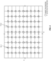
- FIG. 4 illustrates a Cartesian coordinate system as the coordinate system used to determine the positional deviation of each module pin 112 from the respective target position.
- the computer interface of the equipment 300 calculates an X offset for each pin 112 that has a detected position that differs from the corresponding target position in the X axis of the Cartesian coordinate system.
- the equipment 300 also calculates a Y offset for each pin 112 that has a position that differs from the corresponding target position in the Y axis of the Cartesian coordinate system.
- the detected position of some pins 112_1 may be within the corresponding target position whereas the detected position of other pins 112_2 may be outside the corresponding target position.
- the openings 116 in the module housing 106 are typically large enough to accommodate greater pin position tolerance than the openings 202 in the circuit board.
- Each module pin 112_2 that has a detected position outside the corresponding target position in FIG. 4 most likely will not be received by the corresponding opening 202 in the circuit board 200 absent some positional adjustment of the power semiconductor module 100, at least in the case of automated press fitting.
- step (b) in FIG. 3 involves determining a positional offset for the power semiconductor module 100 based on the positional deviations of the individual pins 112.
- a best fit position of all pins 112 is determined for the power semiconductor module 100.
- Best fit is a fitting process that determines the best fit to a series of data points.
- the data points are the positional deviations of the individual module pins 112 and the fitting criteria ensures all module pins 112 are within the respective target positions. If a best fit solution is not possible, then the power semiconductor module is reworked or discarded.
- FIG. 5 illustrates the positional offset for the power semiconductor module 100 within the Cartesian coordinate system, by calculating the positional offset based on the X and Y offsets calculated for the pins 112.
- the calculated best fit reduces overall misalignment between the module pins 112 and the target positions.
- the best fit positional offset indicates a positional shift of the power semiconductor module 100 in the X direction and/or the Y direction that ensures overall better alignment of the pins 112 with the target positions.
- the positional offset may indicate a rotational shift of the power semiconductor module 100.
- the positional offset for the power semiconductor module 100 may result in one or more individual pins 112 having a larger but still acceptable X and/or Y offset with the corresponding target position.
- overall pin alignment for the power semiconductor module 100 is increased and the positional offset yields a collective best fit since all pins 112 fall within the target positions by applying the positional offset.
- Step (C) in FIG. 3 involves encoding the positional offset on an exposed surface of the power semiconductor module 100.
- the encoding is performed by laser equipment 302 that laser marks one or more fiducial marks 130 or a barcode 132 indicative of the positional offset on an exposed surface of the power semiconductor module 100.
- the laser equipment 302 instead may be ink jet printing equipment that ink jet prints one or more fiducial marks 130 or a barcode 132 indicative of the positional offset on an exposed surface of the power semiconductor module 100.
- the laser equipment 302 instead may be mechanical scribe equipment that scribes (cuts or scratches) one or more fiducial marks 130 or a barcode 132 indicative of the positional offset on an exposed surface of the power semiconductor module 100.
- FIGS. 6 through 15 illustrate different embodiments of the positional offset encoded on an exposed surface of the power semiconductor module 100.
- the positional offset is shown encoded as one or more fiducial marks 130.
- the positional offset may be encoded as a barcode 130 or any other form suitable to convey the positional offset information.
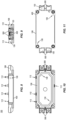
- FIG. 6 illustrates a top plan view of the power semiconductor module 100.
- the positional offset is encoded on an exposed front surface of the module housing 106.
- FIG. 7 illustrates a bottom plan view of the power semiconductor module 100.
- the positional offset is encoded on an exposed back surface of the module 100.
- the positional offset may be encoded on the substrate 104, a metallic baseplate 400, or the housing 106 at the backside of the module 100.
- FIG. 8 illustrates a side view of the power semiconductor module 100.
- the positional offset is encoded on an exposed side surface of the module housing 106.
- FIG. 9 illustrates an end view of the power semiconductor module 100.
- the positional offset is encoded on an exposed end surface of the module housing 106.
- the power semiconductor module 100 has one or more metallic bus bars 500 for providing a reference voltage to the power semiconductor module 100 and/or carrying current to or from the power semiconductor module 100.
- FIG. 10 illustrates a top plan view of the power semiconductor module 100.
- the positional offset is encoded on an exposed front surface of the module housing 106 and the module 100 has one or more metallic bus bars 500 for providing a reference voltage to the power semiconductor module 100 and/or carrying current to or from the power semiconductor module 100.
- FIG. 11 illustrates a bottom plan view of the power semiconductor module 100.
- the positional offset is encoded on an exposed back surface of the metallic baseplate 400 and the module 100 has one or more metallic bus bars 500 for providing a reference voltage to the power semiconductor module 100 and/or carrying current to or from the power semiconductor module 100.
- the positional offset may be encoded on an exposed back surface of one or more of the metallic bus bars 500.
- FIG. 12 illustrates an end view of the power semiconductor module 100. According to this embodiment, the positional offset is encoded on an exposed end surface of the module housing 106.
- FIG. 13 illustrates a side view of the power semiconductor module 100.
- the positional offset is encoded on an exposed side surface of the module housing 106.
- FIG. 14 illustrates a top plan view of the power semiconductor module 100.
- the positional offset is encoded on an exposed front surface of the module housing 106.
- FIG. 15 illustrates a bottom plan view of the power semiconductor module 100.
- the positional offset is encoded on an exposed back surface of the module 100.
- the positional offset may be encoded on an exposed back surface of the module housing 106.
- the positional offset may be encoded on an exposed metallized back surface of the module substrate 104 which may or may not be patterned.
- the positional offset may be encoded on an exposed back surface of the metallic tab(s) 128 provided for anchoring the module 100 to a heat sink (not shown in FIG. 15 ).
- FIG. 16 illustrates an embodiment of a method of mounting the power semiconductor module 100 to a circuit board 400 using automated press tool equipment.
- the automated press tool equipment is prepared for press fitting of the power semiconductor module 100 to the circuit board 200.
- the automated press tool equipment includes a base 600 that may include guide domes or posts 602 for pre-alignment purposes.
- the circuit board 400 is placed into the automated press tool equipment.
- the guide domes or posts 602 of the press tool base 600 may be used to ensure correct placement of the circuit board 400.
- Circuit components 604 may be mounted to the circuit board 400.
- the press tool base 600 may have one or more recesses 606 for receiving the circuit components 604 during the press fitting.
- the automated press tool equipment presses the circuit board 400 against the press tool base 600.
- a moveable part 608 of the automated press tool equipment secures the power semiconductor module 100.
- the positional offset for the power semiconductor module 100 is encoded on an exposed surface of the module 100.
- the positional offset is shown encoded as fiducial marks 130.
- the positional offset may be encoded as a barcode 130 or any other form suitable to convey the positional offset information.
- the automated press tool equipment deciphers the positional offset, e.g., by optical imaging. If a barcode 132 or other type of encoding is used, the automated press tool equipment decodes the encoded information to decipher the positional offset.
- the fiducial marks 130 directly indicate the positional offset.
- the automated press tool equipment adjusts the pressing position of the moveable tool part 608 in relation to the circuit board 400, based on the deciphered positional offset.
- the pressing position of the moveable tool part 608 may be adjusted in the X direction, Y direction and/or along a rotational axis 610 that is parallel to the pressing direction Z.
- the moveable tool part 608 presses the module pins 112 into the respective openings 202 in the circuit board 400.
- step e) this may involve placing the power semiconductor module 100 on the guide domes or posts 602 of the press tool base 600.
- the power semiconductor module 100 may then be released and the module pins 112 inserted into the corresponding openings 202 in the circuit board 200.
- Step f) shows the module pins 112 being inserted into the circuit board openings 202.
- the deformable part 120 of the module pins 112 plastically and/or elastically deform upon insertion into the circuit board openings 202.
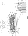
- FIG. 17 illustrates an embodiment of a method of mounting the power semiconductor module 100 to a heat sink 700.
- the heat sink 700 may be air or liquid cooled.
- the power semiconductor module 100 may be mounted to the circuit board 200 before or after the module 100 is mounted to the heat sink 700.
- the circuit board 200 may be provided with additional openings to allow access for the heat sink fasteners 702.
- the holes 704 in the module 100 for receiving the heat sink fasteners 702 are larger than the diameter of the fasteners 702, which allows for some movement of the modules 100 on the heat sink 700 prior to being secured in place. This makes circuit board press fitting more difficult, if the modules 100 are not mounted accurately on the heat sink 700.
- the mounting position of the power semiconductor module 100 to the heat sink 700 is adjusted based on the positional offset encoded on an exterior surface of the module 100 to improve mounting accuracy for the circuit board 400. This may involve imaging equipment 704 reading and deciphering the positional offset encoded on the exterior surface of the module 100, e.g., as described above in connection with FIG. 16 .
- the mounting position of the power semiconductor module 100 to the heat sink 700 may be adjusted based on the positional offset in the X direction, Y direction and/or along a rotational axis 706 that is parallel to the pressing direction Z.
- a best fit calculation may be used to determine the positional offset for the power semiconductor module 100.
- the data points are the positional deviations of the individual module pins 112 and the fitting criteria ensures all module pins 112 are within the respective target positions.
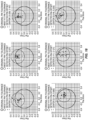
- FIG. 18 illustrates six (6) different Gaussian geometric best fit examples for the module positional offset, calculated based on the positional deviations (offsets) of the individual pins 112.
- a geometric center of gravity may be calculated based on the positional deviations of the pins 112, e.g., based on coordinate shifts in the X and Y directions.
- the positional offset for the power semiconductor module 100 is determined by applying a least squares regression analysis to the positional deviations of the pins 112.
- the positional offset for the power semiconductor module 100 is determined by calculating the positional offset based on the maximum and the minimum positional deviations of the pins 112. In each case, the overall pin tolerance for the power semiconductor module 100 is reduced using the best fit approach which in turn increases overall module pin alignment accuracy relative to the circuit board 200.
- FIG. 19 illustrates another Gaussian best fit example that uses the positional deviations (offsets) of the individual pins 112 to determine the positional offset for the power semiconductor module 100.
- best fit adjustment of the pin tip positions are calculated according to each coordinate center of gravity.
- Example 1 A method of increasing overall pin alignment accuracy for a power semiconductor module having a plurality of pins protruding from a housing of the power semiconductor module, the method comprising: determining a positional deviation of each pin of the plurality of pins from a respective target position in a coordinate system; determining a positional offset for the power semiconductor module based on the positional deviations of the pins, the positional offset reducing overall misalignment between the plurality of pins and the target positions; and encoding the positional offset on an exposed surface of the power semiconductor module.
- Example 2 The method of example 1, wherein determining the positional offset for the power semiconductor module comprises: applying a least squares regression analysis to the positional deviations of the pins.
- Example 3 The method of examples 1 to 2, wherein determining the positional offset for the power semiconductor module comprises: calculating the positional offset based on the maximum and the minimum positional deviations of the pins.
- Example 4 The method of examples 1 to 3, wherein determining the positional offset for the power semiconductor module comprises: calculating a geometric center of gravity based on the positional deviations of the pins.
- Example 5 The method of any of examples 1 through 4, wherein the coordinate system is a Cartesian coordinate system and wherein determining the positional deviation of each pin comprises: calculating an X offset for each pin having a position that differs from the corresponding target position in the X axis of the Cartesian coordinate system; and calculating a Y offset for each pin having a position that differs from the corresponding target position in the Y axis of the Cartesian coordinate system.
- Example 6 The method of example 5, wherein determining the positional offset for the power semiconductor module comprises: calculating the positional offset based on the X and Y offsets calculated for the pins.
- Example 7 The method of any of examples 1 through 6, wherein encoding the positional offset on the exposed surface of the power semiconductor module comprises: marking one or more fiducial marks indicative of the positional offset on the exposed surface of the power semiconductor module.
- Example 8 The method of any of examples 1 through 6, wherein encoding the positional offset on the exposed surface of the power semiconductor module comprises: marking a barcode indicative of the positional offset on the exposed surface of the power semiconductor module.
- Example 9 The method of any of examples 1 through 8, wherein encoding the positional offset on the exposed surface of the power semiconductor module comprises: laser marking one or more fiducial marks or a barcode indicative of the positional offset on the exposed surface of the power semiconductor module.
- Example 10 The method of any of examples 1 through 8, wherein encoding the positional offset on the exposed surface of the power semiconductor module comprises: ink jet printing one or more fiducial marks or a barcode indicative of the positional offset on the exposed surface of the power semiconductor module.
- Example 11 The method of any of examples 1 through 8, wherein encoding the positional offset on the exposed surface of the power semiconductor module comprises: scribing one or more fiducial marks or a barcode indicative of the positional offset on the exposed surface of the power semiconductor module.
- Example 12 The method of any of examples 1 through 11, wherein encoding the positional offset on the exposed surface of the power semiconductor module comprises: encoding the positional offset on an exposed surface of the housing.
- Example 13 The method of any of examples 1 through 11, wherein encoding the positional offset on the exposed surface of the power semiconductor module comprises: encoding the positional offset on an exposed surface of a substrate of the power semiconductor module to which the housing is secured.
- Example 14 The method of any of examples 1 through 11, wherein encoding the positional offset on the exposed surface of the power semiconductor module comprises: encoding the positional offset on an exposed surface of a metallic component of the power semiconductor module.
- Example 15 The method of any of examples 1 through 14, further comprising: deciphering the positional offset encoded on the exposed surface of the power semiconductor module; securing the power semiconductor module by automated equipment; adjusting a pressing position of the automated equipment in relation to a circuit board, based on the deciphered positional offset; and after adjusting the pressing position, pressing the plurality of pins into respective openings in the circuit board via the automated equipment.
- Example 16 The method of any of examples 1 through 15, further comprising: adjusting a mounting position of the power semiconductor module to a heat sink based on the positional offset.
- Example 17 A method of mounting a power semiconductor module having a plurality of pins protruding from a housing of the power semiconductor module, the method comprising: deciphering a positional offset encoded on the exposed surface of the power semiconductor module, the positional offset reducing overall misalignment between the plurality of pins and target positions for the pins; securing the power semiconductor module by automated equipment; adjusting a pressing position of the automated equipment in relation to a circuit board, based on the deciphered positional offset; and after adjusting the pressing position, pressing the plurality of pins into respective openings in the circuit board via the automated equipment.
- Example 18 A power semiconductor module, comprising: a plurality of power semiconductor dies attached to a substrate; a housing secured to the substrate and enclosing the plurality of power semiconductor dies; a plurality of pins protruding from the housing; and a positional offset encoded on the exposed surface of the power semiconductor module, the positional offset reducing overall misalignment between the plurality of pins and target positions for the pins.
- Example 19 The power semiconductor module of example 18, wherein the positional offset encoded on the exposed surface of the power semiconductor module comprises one or more fiducial marks indicative of the positional offset.
- Example 20 The power semiconductor module of example 18, wherein the positional offset encoded on the exposed surface of the power semiconductor module comprises a barcode indicative of the positional offset.
- Example 21 The power semiconductor module of example 20, wherein the barcode relates the positional offset to a plurality of mounting regions of the housing that are configured to enable mounting of the housing to a body.
Landscapes
- Cooling Or The Like Of Semiconductors Or Solid State Devices (AREA)
Abstract
A method of increasing overall pin alignment accuracy for a power semiconductor module is provided. The power semiconductor module has a plurality of pins protruding from a housing of the power semiconductor module. The method includes: determining a positional deviation of each pin of the plurality of pins from a respective target position in a coordinate system; determining a positional offset for the power semiconductor module based on the positional deviations of the pins, the positional offset reducing overall misalignment between the plurality of pins and the target positions; and encoding the positional offset on an exposed surface of the power semiconductor module. Methods of mounting the power semiconductor module to a circuit board and/or heat sink are also provided.
Description
- The present disclosure relates to a power semiconductor module, in particular to a positional offset encoded on a power semiconductor module.
- Power semiconductor modules typically have a current rating between 6A and 3600A (or higher) cover a power range from hundreds of watts to several megawatts, and have wide adoption across many applications such as general purpose drives, traction, servo-units, renewable energy applications like solar inverters or wind applications, hybrid electric and full electric vehicle applications, etc. The electrical connection interface for power semiconductor modules typically includes contact pins that provide an electrical interface between the power semiconductor dies housed in the electrically insulative enclosure of the module and a circuit board with additional electronic components.
- Accurate alignment of the module pins with corresponding openings in the circuit board is necessary to avoid pin and/or board damage during the module mounting process. This typically involves optical detection of the pin tip positions during the module mounting process. Optically scanning the pin tips to determine pin tip position is a complex and slow process, especially for a high number of pins, and dedicated optical inspection equipment and corresponding know-how is required to implement pin tip recognition. Another approach is for a human operator to manually press fit each power semiconductor module to the respective circuit board, which is labor intensive and slow.
- According to an embodiment of a method of increasing overall pin alignment accuracy for a power semiconductor module having a plurality of pins protruding from a housing of the power semiconductor module, the method comprises: determining a positional deviation of each pin of the plurality of pins from a respective target position in a coordinate system; determining a positional offset for the power semiconductor module based on the positional deviations of the pins, the positional offset reducing overall misalignment between the plurality of pins and the target positions; and encoding the positional offset on an exposed surface of the power semiconductor module.
- According to an embodiment of a method of mounting a power semiconductor module having a plurality of pins protruding from a housing of the power semiconductor module, the method comprises: deciphering a positional offset encoded on the exposed surface of the power semiconductor module, the positional offset reducing overall misalignment between the plurality of pins and target positions for the pins; securing the power semiconductor module by automated equipment; adjusting a pressing position of the automated equipment in relation to a circuit board, based on the deciphered positional offset; and after adjusting the pressing position, pressing the plurality of pins into respective openings in the circuit board via the automated equipment.
- According to an embodiment of a power semiconductor module, the power semiconductor module comprises: a plurality of power semiconductor dies attached to a substrate; a housing secured to the substrate and enclosing the plurality of power semiconductor dies; a plurality of pins protruding from the housing; and a positional offset encoded on the exposed surface of the power semiconductor module, the positional offset reducing overall misalignment between the plurality of pins and target positions for the pins.
- Those skilled in the art will recognize additional features and advantages upon reading the following detailed description, and upon viewing the accompanying drawings.
- The elements of the drawings are not necessarily to scale relative to each other. Like reference numerals designate corresponding similar parts. The features of the various illustrated embodiments can be combined unless they exclude each other. Embodiments are depicted in the drawings and are detailed in the description which follows.
-
FIG. 1 illustrates an exploded view of a power semiconductor module having an encoded positional offset that increases overall pin alignment accuracy for the module. -
FIGS. 2A and 2B illustrate two different pin alignment scenarios for the power semiconductor module. -
FIG. 3 illustrates an embodiment of increasing overall pin alignment accuracy for the power semiconductor module by encoding a positional offset on an exposed surface of the module. -
FIG. 4 illustrates a Cartesian coordinate system used as the coordinate system to determine the positional deviation of each module pin from a respective target position. -
FIG. 5 illustrates the positional offset for the power semiconductor module within the Cartesian coordinate system, by calculating the positional offset based on the X and Y offsets calculated for the pins. -
FIGS. 6 through 15 illustrate different embodiments of the positional offset encoded on an exposed surface of the power semiconductor module. -
FIG. 16 illustrates an embodiment of a method of mounting the power semiconductor module to a circuit board using automated press tool equipment. -
FIG. 17 illustrates an embodiment of a method of mounting the power semiconductor module to a heat sink. -
FIG. 18 illustrates six (6) different Gaussian geometric best fit examples for the module positional offset, calculated based on the positional deviations (offsets) of the individual module pins. -
FIG. 19 illustrates another Gaussian best fit example that uses the positional deviations (offsets) of theindividual module pins 112 to determine the positional offset for the power semiconductor module. - According to embodiments described herein, a positional offset is encoded on an exposed surface of a power semiconductor module that reduces overall misalignment between the module pins and target positions for the pins. A method of increasing overall pin alignment accuracy for the power semiconductor module and a method of mounting the power semiconductor module to a circuit board and/or a heat sink are also described. The encoded positional offset can be used to adjust a pressing position of automated equipment in relation to a circuit board, to reduce overall misalignment between the module pins and corresponding openings (apertures) in a circuit board when the automated equipment presses the module pins into the board openings. By encoding the positional offset on an exposed surface of the power semiconductor module, the individual pin tip positions do not need to be optically scanned during the module mounting process. Instead, the encoded positional offset simply needs to be ascertained from the exposed surface of the power semiconductor module and deciphered to determine an optimal pressing position for the power semiconductor module.
- Described next, with reference to the figures, are exemplary embodiments of the power semiconductor module with the encoded positional offset and methods of mounting the power semiconductor module. Any of the power semiconductor module and method embodiments described herein may be used interchangeably unless otherwise expressly stated.
-
FIG. 1 illustrates an exploded view of apower semiconductor module 100. Thepower semiconductor module 100 may form part of a power electronics circuit for use in various power applications such as a DC/AC inverter, a DC/DC converter, an AC/DC converter, a DC/AC converter, an AC/AC converter, a multi-phase inverter, an H-bridge, motor drive, etc. Thepower semiconductor module 100 includes power semiconductor dies 102 attached to asubstrate 104. An electricallyinsulative housing 106 is secured to thesubstrate 104 as indicated by the downward facing arrows inFIG. 1 , and encloses the power semiconductor dies 102. In the case of aplastic housing 106, thehousing 106 may be secured to thesubstrate 104 by an adhesive, plastic cement, etc. - The
substrate 104 may be, e.g., a DCB (direct copper bonded) substrate, an AMB (active metal brazed) substrate, an IMS (insulated metal substrate), etc. In the case of DCB, AMB, or IMS substrate technologies, thesubstrate 104 may include aceramic body 108 with a patternedmetallization 110 on the frontside of theceramic body 108 and to which the power semiconductor dies 102 are attached, e.g., by solder, sintering, an adhesive, etc. - The power semiconductor dies 102 may be electrically contacted at the backside by the
patterned metallization 110 of thesubstrate 104 and at the frontside bybond wires 112, metal clips (not shown), etc. The power semiconductor dies 102 may include power Si or SiC power MOSFET (metal-oxide-semiconductor field-effect transistor) dies, HEMT (high-electron mobility transistor) dies, IGBT (insulated-gate bipolar transistor) dies, JFET (junction filed-effect transistor) dies, power diode dies, etc. Some or all of the power semiconductor dies 102 may be, e.g., vertical power transistor dies. For a vertical power transistor die, the primary current flow path is between the front and back sides of the die. The drain pad is typically disposed at the backside of the die, with the gate and source pads (and optionally one or more sense pads) at the frontside of the die. Additional types of semiconductor dies may be included in thepower semiconductor module 100, e.g., such as one or more logic dies, controller dies, gate driver dies, etc. - The
power semiconductor module 100 also includespins 112 that protrude from thehousing 106. Thepins 112 are attached to thesubstrate 104 and/or another structure such as a metallic lead frame or clip frame enclosed by thehousing 106, and protrude through afirst side 114 of thehousing 106 to form an electrical connection interface outside thehousing 106. Thepins 112 extend throughopenings 118 in thefirst side 114 of thehousing 106. - In one embodiment, the
pins 112 are press-fit pins, The term 'press-fit' as used herein refers to a pin geometry that enables plastic and/or elastic deformation in an upper region of thepins 112 when thepins 112 are inserted into corresponding openings of a circuit board (not shown inFIG. 1 ) such as a PCB (printed circuit board) or other type of component, providing effective contact points within the contact zone. The contact radius increases due to the contact pressure since the macroscopic contact force concentrates on a microscopic contact area. Accordingly, the pin face and the metallized face of the opening of the circuit board merge, i.e., are cold welded. Such a press-fit connection increases the effective contact zone and may provide a gas-tight contact zone that is robust against corrosive environments. - In the case of press-
fit pins 112, thepins 112 include atip part 118 configured to guide the press-fit pin 112 into a respective opening of a circuit board. Adeformable part 120 adjoins thetip part 118 and is configured to plastically and/or elastically deform upon insertion into the corresponding circuit board opening. Anelongate part 122 adjoins thedeformable part 120 and has a length that may be chosen to accommodate the thickness (height) of themodule housing 106 through which the press-fit pin 112 protrudes. Abase part 124 adjoins theelongate part 122 and may be the widest part of the press-fit pin 112 to accommodate a force applied to thebase part 124 for pressing thepin 112 into asleeve 126 attached to thesubstrate 104. An anchoring part (out-of-view inFIG. 1 ) adjoins thebase part 124 and is received by thecorresponding sleeve 126. - Part of a metallic lead frame or clip frame included (not shown in
FIG. 1 ) in thepower semiconductor module 100 may protrude through one or more side faces of thehousing 106 to form a power terminal which may provide a reference voltage to thepower semiconductor module 100 or carry current to or from thepower semiconductor module 100. The electrical connection interface formed by thepins 112 provides an electrical interface to the power semiconductor dies 102 enclosed by thehousing 106. As explained above, thepins 112 may have a pin geometry that enables plastic and/or elastic deformation of adeformable part 120 of thepins 112 upon insertion of the tip-end 118 of thepins 112 into corresponding openings of a circuit board. One or moremetallic tabs 128 or similar anchoring structures may protrude from thehousing 106 to provide an anchoring point for securing thepower semiconductor module 100 to a heat sink (not shown inFIG. 1 ). -
FIGS. 2A and 2B illustrate two different pin alignment scenarios for thepower semiconductor module 100. During mounting of thepower semiconductor module 100 to acircuit board 200 such as a PCB, all module pins 112 should be received by respective (apertures)openings 202 in thecircuit board 200. InFIG. 2A , thevertical centerline 204 of the illustratedpin tip 118 is offset from thevertical centerline 206 of the corresponding circuit board opening 202 but by an acceptable amount Δx1. Accordingly, thepin 112 inFIG. 2A is properly received by the corresponding circuit board opening 202 during press fitting of thepower semiconductor module 100. - In
FIG. 2B , thevertical centerline 204 of the illustratedpin tip 118 also is offset from thevertical centerline 206 of the correspondingcircuit board opening 202 by an amount Δx2 that is outside the permitted alignment tolerance. Accordingly, thepin 112 inFIG. 2B is not received by the corresponding circuit board opening 202 during press fitting of thepower semiconductor module 100 which results in damage to thepin 112 and/orcircuit board 200. - To avoid the misalignment issue illustrated in
FIG. 2B , a positional offset is encoded on an exposed surface of thepower semiconductor module 100. The positional offset reduces the overall misalignment between thepins 112 and target positions for thepins 112. The encoded positional offset can be used to adjust a pressing position of automated equipment (not shown inFIGS. 2A and 2B ) in relation to thecircuit board 200, to reduce overall misalignment between the module pins 112 andcorresponding openings 202 in thecircuit board 200 when the automated equipment presses the module pins 112 into theboard openings 202 as indicated by the upward facing arrows inFIGS. 2A and 2B . -
FIG. 1 illustrates different embodiments of the positional offset encoded on an exposed surface of thepower semiconductor module 100. For example, the positional offset may include one or morefiducial marks 130 indicative of the positional offset. Eachfiducial mark 130 is decipherable by an imaging system and may be used as a point of reference for adjusting the position (X, Y and/or rotational) of thepower semiconductor module 100 during module mounting to ensure pin alignment accuracy. In another example, the positional offset may include abarcode 132 indicative of the positional offset. Thebarcode 132 may be (linear) one-dimensional or (matrix) two-dimensional. Thebarcode 132 is decipherable by a barcode reader system and may be used to indicate a positional (X, Y and/or rotational) shift for thepower semiconductor module 100 during module mounting to ensure pin alignment accuracy. - The
barcode 132 may relate the positional offset to a plurality of mountingregions 134 of thehousing 106. The mountingregions 106 are configured to enable mounting of thehousing 106 to a body such a circuit board, heat sink, etc. For example, the mountingregions 106 may be used to locate the module housing during PCB installation (e.g., as shown inFIG. 16 ) and may also be used after PCB installation, e.g., to secure the PCB to thehousing 106 with screws, for example. In each case, alignment instructions indicated by the positional offset may be encoded in thebarcode 132 such that thebarcode 132 relates the positional offset to the mountingregions 134 of thehousing 106. Thebarcode 132 may instead relate the positional offset to other features already present on thehousing 106, e.g., such as pegs or through holes. In each of these examples, thefiducial mark 130 is not necessary to implement the alignment instructions indicated by the positional offset. - In each case, the positional offset encoded on an exposed surface of the
power semiconductor module 100 reduces overall misalignment between the module pins 112 and target positions for the module pins 112. For example, during mounting of thepower semiconductor module 100 to thecircuit board 200 shown inFIGS. 2A and 2B , the positional offset may be deciphered and used to adjust a pressing position of automated equipment (not shown inFIGS. 2A and 2B ) in relation to thecircuit board 200 such that all pins 112 of thepower semiconductor module 100 are received by therespective openings 202 in thecircuit board 200. -
FIG. 3 illustrates an embodiment of increasing overall pin alignment accuracy for thepower semiconductor module 100 by encoding the positional offset on an exposed surface of thepower semiconductor module 100. In step (a),equipment 300 such as optical scanning equipment and a corresponding computer interface is used to determine a positional deviation of eachmodule pin 112 from a respective target position in a coordinate system. Theequipment 300 determines the position of eachpin 112, e.g., by optical scanning and uses the pin position information to determine whether thepin 112 has any positional deviation from the respective target position in the coordinate system. -
FIG. 4 illustrates a Cartesian coordinate system as the coordinate system used to determine the positional deviation of eachmodule pin 112 from the respective target position. According to this embodiment, the computer interface of theequipment 300 calculates an X offset for eachpin 112 that has a detected position that differs from the corresponding target position in the X axis of the Cartesian coordinate system. Theequipment 300 also calculates a Y offset for eachpin 112 that has a position that differs from the corresponding target position in the Y axis of the Cartesian coordinate system. - As shown in
FIG. 4 , the detected position of some pins 112_1 may be within the corresponding target position whereas the detected position of other pins 112_2 may be outside the corresponding target position. Theopenings 116 in themodule housing 106 are typically large enough to accommodate greater pin position tolerance than theopenings 202 in the circuit board. Each module pin 112_2 that has a detected position outside the corresponding target position inFIG. 4 most likely will not be received by thecorresponding opening 202 in thecircuit board 200 absent some positional adjustment of thepower semiconductor module 100, at least in the case of automated press fitting. - To mitigate this issue, step (b) in
FIG. 3 involves determining a positional offset for thepower semiconductor module 100 based on the positional deviations of the individual pins 112. In one embodiment, a best fit position of allpins 112 is determined for thepower semiconductor module 100. Best fit is a fitting process that determines the best fit to a series of data points. In this case, the data points are the positional deviations of the individual module pins 112 and the fitting criteria ensures all module pins 112 are within the respective target positions. If a best fit solution is not possible, then the power semiconductor module is reworked or discarded. -
FIG. 5 illustrates the positional offset for thepower semiconductor module 100 within the Cartesian coordinate system, by calculating the positional offset based on the X and Y offsets calculated for thepins 112. The calculated best fit reduces overall misalignment between the module pins 112 and the target positions. As shown inFIG. 5 , the best fit positional offset indicates a positional shift of thepower semiconductor module 100 in the X direction and/or the Y direction that ensures overall better alignment of thepins 112 with the target positions. Separately or in combination, the positional offset may indicate a rotational shift of thepower semiconductor module 100. - As is evident by comparing
FIGS. 4 and5 , the positional offset for thepower semiconductor module 100 may result in one or moreindividual pins 112 having a larger but still acceptable X and/or Y offset with the corresponding target position. However, overall pin alignment for thepower semiconductor module 100 is increased and the positional offset yields a collective best fit since all pins 112 fall within the target positions by applying the positional offset. - Step (C) in
FIG. 3 involves encoding the positional offset on an exposed surface of thepower semiconductor module 100. InFIG. 3 , the encoding is performed bylaser equipment 302 that laser marks one or morefiducial marks 130 or abarcode 132 indicative of the positional offset on an exposed surface of thepower semiconductor module 100. Thelaser equipment 302 instead may be ink jet printing equipment that ink jet prints one or morefiducial marks 130 or abarcode 132 indicative of the positional offset on an exposed surface of thepower semiconductor module 100. In still another embodiment, thelaser equipment 302 instead may be mechanical scribe equipment that scribes (cuts or scratches) one or morefiducial marks 130 or abarcode 132 indicative of the positional offset on an exposed surface of thepower semiconductor module 100. -
FIGS. 6 through 15 illustrate different embodiments of the positional offset encoded on an exposed surface of thepower semiconductor module 100. InFIGS. 6 through 15 , the positional offset is shown encoded as one or morefiducial marks 130. Instead, the positional offset may be encoded as abarcode 130 or any other form suitable to convey the positional offset information. -
FIG. 6 illustrates a top plan view of thepower semiconductor module 100. According to this embodiment, the positional offset is encoded on an exposed front surface of themodule housing 106. -
FIG. 7 illustrates a bottom plan view of thepower semiconductor module 100. According to this embodiment, the positional offset is encoded on an exposed back surface of themodule 100. For example, the positional offset may be encoded on thesubstrate 104, ametallic baseplate 400, or thehousing 106 at the backside of themodule 100. -
FIG. 8 illustrates a side view of thepower semiconductor module 100. According to this embodiment, the positional offset is encoded on an exposed side surface of themodule housing 106. -
FIG. 9 illustrates an end view of thepower semiconductor module 100. According to this embodiment, the positional offset is encoded on an exposed end surface of themodule housing 106. Also in this embodiment, thepower semiconductor module 100 has one or moremetallic bus bars 500 for providing a reference voltage to thepower semiconductor module 100 and/or carrying current to or from thepower semiconductor module 100. -
FIG. 10 illustrates a top plan view of thepower semiconductor module 100. According to this embodiment, the positional offset is encoded on an exposed front surface of themodule housing 106 and themodule 100 has one or moremetallic bus bars 500 for providing a reference voltage to thepower semiconductor module 100 and/or carrying current to or from thepower semiconductor module 100. -
FIG. 11 illustrates a bottom plan view of thepower semiconductor module 100. According to this embodiment, the positional offset is encoded on an exposed back surface of themetallic baseplate 400 and themodule 100 has one or moremetallic bus bars 500 for providing a reference voltage to thepower semiconductor module 100 and/or carrying current to or from thepower semiconductor module 100. Separately or in combination, the positional offset may be encoded on an exposed back surface of one or more of the metallic bus bars 500. -
FIG. 12 illustrates an end view of thepower semiconductor module 100. According to this embodiment, the positional offset is encoded on an exposed end surface of themodule housing 106. -
FIG. 13 illustrates a side view of thepower semiconductor module 100. According to this embodiment, the positional offset is encoded on an exposed side surface of themodule housing 106. -
FIG. 14 illustrates a top plan view of thepower semiconductor module 100. According to this embodiment, the positional offset is encoded on an exposed front surface of themodule housing 106. -
FIG. 15 illustrates a bottom plan view of thepower semiconductor module 100. According to this embodiment, the positional offset is encoded on an exposed back surface of themodule 100. For example, the positional offset may be encoded on an exposed back surface of themodule housing 106. Separately or in combination, the positional offset may be encoded on an exposed metallized back surface of themodule substrate 104 which may or may not be patterned. Separately or in combination, the positional offset may be encoded on an exposed back surface of the metallic tab(s) 128 provided for anchoring themodule 100 to a heat sink (not shown inFIG. 15 ). -
FIG. 16 illustrates an embodiment of a method of mounting thepower semiconductor module 100 to acircuit board 400 using automated press tool equipment. In step a), the automated press tool equipment is prepared for press fitting of thepower semiconductor module 100 to thecircuit board 200. The automated press tool equipment includes a base 600 that may include guide domes orposts 602 for pre-alignment purposes. In step b), thecircuit board 400 is placed into the automated press tool equipment. The guide domes orposts 602 of thepress tool base 600 may be used to ensure correct placement of thecircuit board 400.Circuit components 604 may be mounted to thecircuit board 400. In this case, thepress tool base 600 may have one ormore recesses 606 for receiving thecircuit components 604 during the press fitting. In step c), the automated press tool equipment presses thecircuit board 400 against thepress tool base 600. - In step d), a
moveable part 608 of the automated press tool equipment secures thepower semiconductor module 100. The positional offset for thepower semiconductor module 100 is encoded on an exposed surface of themodule 100. InFIG. 16 , the positional offset is shown encoded asfiducial marks 130. Instead, the positional offset may be encoded as abarcode 130 or any other form suitable to convey the positional offset information. The automated press tool equipment deciphers the positional offset, e.g., by optical imaging. If abarcode 132 or other type of encoding is used, the automated press tool equipment decodes the encoded information to decipher the positional offset. In the case offiducial marks 130, thefiducial marks 130 directly indicate the positional offset. - In each case, the automated press tool equipment adjusts the pressing position of the
moveable tool part 608 in relation to thecircuit board 400, based on the deciphered positional offset. The pressing position of themoveable tool part 608 may be adjusted in the X direction, Y direction and/or along arotational axis 610 that is parallel to the pressing direction Z. After adjusting the pressing position of themoveable tool part 608, themoveable tool part 608 presses the module pins 112 into therespective openings 202 in thecircuit board 400. In step e), this may involve placing thepower semiconductor module 100 on the guide domes orposts 602 of thepress tool base 600. Thepower semiconductor module 100 may then be released and the module pins 112 inserted into the correspondingopenings 202 in thecircuit board 200. Step f) shows the module pins 112 being inserted into thecircuit board openings 202. In the case of press-fit pins, thedeformable part 120 of the module pins 112 plastically and/or elastically deform upon insertion into thecircuit board openings 202. -
FIG. 17 illustrates an embodiment of a method of mounting thepower semiconductor module 100 to aheat sink 700. Theheat sink 700 may be air or liquid cooled. Thepower semiconductor module 100 may be mounted to thecircuit board 200 before or after themodule 100 is mounted to theheat sink 700. When mounted beforehand, thecircuit board 200 may be provided with additional openings to allow access for theheat sink fasteners 702. - Mounting more than one
power semiconductor module 100 to thesame heat sink 700 exasperates the high pin tolerance issue, since thesame circuit board 200 is mounted to the opposite side of themodules 100 as theheat sink 700. Theholes 704 in themodule 100 for receiving theheat sink fasteners 702 are larger than the diameter of thefasteners 702, which allows for some movement of themodules 100 on theheat sink 700 prior to being secured in place. This makes circuit board press fitting more difficult, if themodules 100 are not mounted accurately on theheat sink 700. - Before the
power semiconductor module 100 is mounted to theheat sink 700 using theheat sink fasteners 702, the mounting position of thepower semiconductor module 100 to theheat sink 700 is adjusted based on the positional offset encoded on an exterior surface of themodule 100 to improve mounting accuracy for thecircuit board 400. This may involveimaging equipment 704 reading and deciphering the positional offset encoded on the exterior surface of themodule 100, e.g., as described above in connection withFIG. 16 . The mounting position of thepower semiconductor module 100 to theheat sink 700 may be adjusted based on the positional offset in the X direction, Y direction and/or along arotational axis 706 that is parallel to the pressing direction Z. - As previously explained herein, a best fit calculation may be used to determine the positional offset for the
power semiconductor module 100. In this case, the data points are the positional deviations of the individual module pins 112 and the fitting criteria ensures all module pins 112 are within the respective target positions. -
FIG. 18 illustrates six (6) different Gaussian geometric best fit examples for the module positional offset, calculated based on the positional deviations (offsets) of the individual pins 112. A geometric center of gravity may be calculated based on the positional deviations of thepins 112, e.g., based on coordinate shifts in the X and Y directions. In another embodiment, the positional offset for thepower semiconductor module 100 is determined by applying a least squares regression analysis to the positional deviations of thepins 112. In another embodiment, the positional offset for thepower semiconductor module 100 is determined by calculating the positional offset based on the maximum and the minimum positional deviations of thepins 112. In each case, the overall pin tolerance for thepower semiconductor module 100 is reduced using the best fit approach which in turn increases overall module pin alignment accuracy relative to thecircuit board 200. -
FIG. 19 illustrates another Gaussian best fit example that uses the positional deviations (offsets) of theindividual pins 112 to determine the positional offset for thepower semiconductor module 100. According to this embodiment, best fit adjustment of the pin tip positions are calculated according to each coordinate center of gravity. - Although the present disclosure is not so limited, the following numbered examples demonstrate one or more aspects of the disclosure.
- Example 1. A method of increasing overall pin alignment accuracy for a power semiconductor module having a plurality of pins protruding from a housing of the power semiconductor module, the method comprising: determining a positional deviation of each pin of the plurality of pins from a respective target position in a coordinate system; determining a positional offset for the power semiconductor module based on the positional deviations of the pins, the positional offset reducing overall misalignment between the plurality of pins and the target positions; and encoding the positional offset on an exposed surface of the power semiconductor module.
- Example 2. The method of example 1, wherein determining the positional offset for the power semiconductor module comprises: applying a least squares regression analysis to the positional deviations of the pins.
- Example 3. The method of examples 1 to 2, wherein determining the positional offset for the power semiconductor module comprises: calculating the positional offset based on the maximum and the minimum positional deviations of the pins.
- Example 4. The method of examples 1 to 3, wherein determining the positional offset for the power semiconductor module comprises: calculating a geometric center of gravity based on the positional deviations of the pins.
- Example 5. The method of any of examples 1 through 4, wherein the coordinate system is a Cartesian coordinate system and wherein determining the positional deviation of each pin comprises: calculating an X offset for each pin having a position that differs from the corresponding target position in the X axis of the Cartesian coordinate system; and calculating a Y offset for each pin having a position that differs from the corresponding target position in the Y axis of the Cartesian coordinate system.
- Example 6. The method of example 5, wherein determining the positional offset for the power semiconductor module comprises: calculating the positional offset based on the X and Y offsets calculated for the pins.
- Example 7. The method of any of examples 1 through 6, wherein encoding the positional offset on the exposed surface of the power semiconductor module comprises: marking one or more fiducial marks indicative of the positional offset on the exposed surface of the power semiconductor module.
- Example 8. The method of any of examples 1 through 6, wherein encoding the positional offset on the exposed surface of the power semiconductor module comprises: marking a barcode indicative of the positional offset on the exposed surface of the power semiconductor module.
- Example 9. The method of any of examples 1 through 8, wherein encoding the positional offset on the exposed surface of the power semiconductor module comprises: laser marking one or more fiducial marks or a barcode indicative of the positional offset on the exposed surface of the power semiconductor module.
- Example 10. The method of any of examples 1 through 8, wherein encoding the positional offset on the exposed surface of the power semiconductor module comprises: ink jet printing one or more fiducial marks or a barcode indicative of the positional offset on the exposed surface of the power semiconductor module.
- Example 11. The method of any of examples 1 through 8, wherein encoding the positional offset on the exposed surface of the power semiconductor module comprises: scribing one or more fiducial marks or a barcode indicative of the positional offset on the exposed surface of the power semiconductor module.
- Example 12. The method of any of examples 1 through 11, wherein encoding the positional offset on the exposed surface of the power semiconductor module comprises: encoding the positional offset on an exposed surface of the housing.
- Example 13. The method of any of examples 1 through 11, wherein encoding the positional offset on the exposed surface of the power semiconductor module comprises: encoding the positional offset on an exposed surface of a substrate of the power semiconductor module to which the housing is secured.
- Example 14. The method of any of examples 1 through 11, wherein encoding the positional offset on the exposed surface of the power semiconductor module comprises: encoding the positional offset on an exposed surface of a metallic component of the power semiconductor module.
- Example 15. The method of any of examples 1 through 14, further comprising: deciphering the positional offset encoded on the exposed surface of the power semiconductor module; securing the power semiconductor module by automated equipment; adjusting a pressing position of the automated equipment in relation to a circuit board, based on the deciphered positional offset; and after adjusting the pressing position, pressing the plurality of pins into respective openings in the circuit board via the automated equipment.
- Example 16. The method of any of examples 1 through 15, further comprising: adjusting a mounting position of the power semiconductor module to a heat sink based on the positional offset.
- Example 17. A method of mounting a power semiconductor module having a plurality of pins protruding from a housing of the power semiconductor module, the method comprising: deciphering a positional offset encoded on the exposed surface of the power semiconductor module, the positional offset reducing overall misalignment between the plurality of pins and target positions for the pins; securing the power semiconductor module by automated equipment; adjusting a pressing position of the automated equipment in relation to a circuit board, based on the deciphered positional offset; and after adjusting the pressing position, pressing the plurality of pins into respective openings in the circuit board via the automated equipment.
- Example 18. A power semiconductor module, comprising: a plurality of power semiconductor dies attached to a substrate; a housing secured to the substrate and enclosing the plurality of power semiconductor dies; a plurality of pins protruding from the housing; and a positional offset encoded on the exposed surface of the power semiconductor module, the positional offset reducing overall misalignment between the plurality of pins and target positions for the pins.
- Example 19. The power semiconductor module of example 18, wherein the positional offset encoded on the exposed surface of the power semiconductor module comprises one or more fiducial marks indicative of the positional offset.
- Example 20. The power semiconductor module of example 18, wherein the positional offset encoded on the exposed surface of the power semiconductor module comprises a barcode indicative of the positional offset.
- Example 21. The power semiconductor module of example 20, wherein the barcode relates the positional offset to a plurality of mounting regions of the housing that are configured to enable mounting of the housing to a body.
- Terms such as "first", "second", and the like, are used to describe various elements, regions, sections, etc. and are also not intended to be limiting. Like terms refer to like elements throughout the description.
- As used herein, the terms "having", "containing", "including", "comprising" and the like are open ended terms that indicate the presence of stated elements or features, but do not preclude additional elements or features. The articles "a", "an" and "the" are intended to include the plural as well as the singular, unless the context clearly indicates otherwise.
- The expression "and/or" should be interpreted to include all possible conjunctive and disjunctive combinations, unless expressly noted otherwise. For example, the expression "A and/or B" should be interpreted to mean only A, only B, or both A and B. The expression "at least one of" should be interpreted in the same manner as "and/or", unless expressly noted otherwise. For example, the expression "at least one of A and B" should be interpreted to mean only A, only B, or both A and B.
- It is to be understood that the features of the various embodiments described herein may be combined with each other, unless specifically noted otherwise.
- Although specific embodiments have been illustrated and described herein, it will be appreciated by those of ordinary skill in the art that a variety of alternate and/or equivalent implementations may be substituted for the specific embodiments shown and described without departing from the scope of the present invention. This application is intended to cover any adaptations or variations of the specific embodiments discussed herein. Therefore, it is intended that this invention be limited only by the claims and the equivalents thereof.
Claims (21)
- A method of increasing overall pin alignment accuracy for a power semiconductor module (100) having a plurality of pins (112) protruding from a housing (106) of the power semiconductor module (100), the method comprising:determining a positional deviation of each pin of the plurality of pins (112) from a respective target position in a coordinate system;determining a positional offset for the power semiconductor module (100) based on the positional deviations of the pins (112), the positional offset reducing overall misalignment between the plurality of pins (112) and the target positions; andencoding the positional offset on an exposed surface of the power semiconductor module (100).
- The method of claim 1, wherein determining the positional offset for the power semiconductor module (100) comprises:
applying a least squares regression analysis to the positional deviations of the pins (112). - The method of claims 1 to 2, wherein determining the positional offset for the power semiconductor module (100) comprises:
calculating the positional offset based on the maximum and the minimum positional deviations of the pins (112). - The method of claims 1 to 3, wherein determining the positional offset for the power semiconductor module (100) comprises:
calculating a geometric center of gravity based on the positional deviations of the pins (112). - The method of claims 1 to 4, wherein the coordinate system is a Cartesian coordinate system and wherein determining the positional deviation of each pin (112) comprises:calculating an X offset for each pin (112) having a position that differs from the corresponding target position in the X axis of the Cartesian coordinate system; andcalculating a Y offset for each pin (112) having a position that differs from the corresponding target position in the Y axis of the Cartesian coordinate system.
- The method of claim 5, wherein determining the positional offset for the power semiconductor module comprises:
calculating the positional offset based on the X and Y offsets calculated for the pins (112). - The method of any previous claims 1 to 6, wherein encoding the positional offset on the exposed surface of the power semiconductor module (100) comprises:
marking one or more fiducial (130) marks indicative of the positional offset on the exposed surface of the power semiconductor module (100). - The method of any previous claims 1 to 6, wherein encoding the positional offset on the exposed surface of the power semiconductor module comprises:
marking a barcode (132) indicative of the positional offset on the exposed surface of the power semiconductor module (100). - The method of any previous claims 1 to 8, wherein encoding the positional offset on the exposed surface of the power semiconductor module comprises:
laser marking one or more fiducial marks (130) or a barcode (132) indicative of the positional offset on the exposed surface of the power semiconductor module (100). - The method of any previous claims 1 to 8, wherein encoding the positional offset on the exposed surface of the power semiconductor module (100) comprises:
ink jet printing one or more fiducial marks (130) or a barcode (132) indicative of the positional offset on the exposed surface of the power semiconductor module (100). - The method of any previous claims 1 to 8, wherein encoding the positional offset on the exposed surface of the power semiconductor module (100) comprises:
scribing one or more fiducial marks (130) or a barcode (132) indicative of the positional offset on the exposed surface of the power semiconductor module (100). - The method of any previous claims 1 to 11, wherein encoding the positional offset on the exposed surface of the power semiconductor module (100) comprises:
encoding the positional offset on an exposed surface of the housing (106). - The method of any previous claims 1 to 11, wherein encoding the positional offset on the exposed surface of the power semiconductor module (100) comprises:
encoding the positional offset on an exposed surface of a substrate (104) of the power semiconductor module (100) to which the housing (106) is secured. - The method of any previous claims 1 to 11, wherein encoding the positional offset on the exposed surface of the power semiconductor module (100) comprises:
encoding the positional offset on an exposed surface of a metallic component (400,500) of the power semiconductor module (100). - The method of any previous claims 1 to 14, further comprising:deciphering the positional offset encoded on the exposed surface of the power semiconductor module (100);securing the power semiconductor module (100) by an automated equipment;adjusting a pressing position of the automated equipment in relation to a circuit board (400), based on the deciphered positional offset; andafter adjusting the pressing position, pressing the plurality of pins (112) into respective openings (202) in the circuit board (400) via the automated equipment.
- The method of any previous claims 1 to 15, further comprising:
adjusting a mounting position of the power semiconductor module (100 to a heat sink (700) based on the positional offset. - A method of mounting a power semiconductor module (100) having a plurality of pins (112) protruding from a housing (106) of the power semiconductor module (100), the method comprising:deciphering a positional offset encoded on the exposed surface of the power semiconductor module (100), the positional offset reducing overall misalignment between the plurality of pins (112) and target positions for the pins;securing the power semiconductor module (100) by an automated equipment;adjusting a pressing position of the automated equipment in relation to a circuit board (400), based on the deciphered positional offset; andafter adjusting the pressing position, pressing the plurality of pins (112) into respective openings (202) in the circuit board (400) via the automated equipment.
- A power semiconductor module (100), comprising:a plurality of power semiconductor dies (102) attached to a substrate (104);a housing (106) secured to the substrate (104) and enclosing the plurality of power semiconductor dies (102);a plurality of pins (112) protruding from the housing (106); anda positional offset encoded on the exposed surface of the power semiconductor module (100), the positional offset reducing overall misalignment between the plurality of pins (112) and target positions for the pins.
- The power semiconductor module of claim 18, wherein the positional offset encoded on the exposed surface of the power semiconductor module (100) comprises one or more fiducial marks (130) indicative of the positional offset.
- The power semiconductor module of claim 18, wherein the positional offset encoded on the exposed surface of the power semiconductor module (100) comprises a barcode (132) indicative of the positional offset.
- The power semiconductor module of claim 20, wherein the barcode (132) relates the positional offset to a plurality of mounting regions (134) of the housing (106) that are configured to enable mounting of the housing (106) to a body.
Applications Claiming Priority (1)
| Application Number | Priority Date | Filing Date | Title |
|---|---|---|---|
| US18/326,543 US12494440B2 (en) | 2023-05-31 | 2023-05-31 | Power semiconductor module and method of increasing pin alignment accuracy for power semiconductor modules |
Publications (1)
| Publication Number | Publication Date |
|---|---|
| EP4478408A1 true EP4478408A1 (en) | 2024-12-18 |
Family
ID=91226728
Family Applications (1)
| Application Number | Title | Priority Date | Filing Date |
|---|---|---|---|
| EP24177431.4A Pending EP4478408A1 (en) | 2023-05-31 | 2024-05-22 | Power semiconductor module and method of increasing pin alignment accuracy for power semiconductor modules |
Country Status (3)
| Country | Link |
|---|---|
| US (1) | US12494440B2 (en) |
| EP (1) | EP4478408A1 (en) |
| CN (1) | CN119069406A (en) |
Citations (3)
| Publication number | Priority date | Publication date | Assignee | Title |
|---|---|---|---|---|
| DE102013100701A1 (en) * | 2013-01-24 | 2014-07-24 | Infineon Technologies Ag | SEMICONDUCTOR MODULE ASSEMBLY AND METHOD FOR PRODUCING A SEMICONDUCTOR MODULE ASSEMBLY |
| US20160372392A1 (en) * | 2015-06-18 | 2016-12-22 | Fuji Electric Co., Ltd. | Semiconductor device and semiconductor device fabrication method |
| US20200176351A1 (en) * | 2018-11-30 | 2020-06-04 | Infineon Technologies Ag | Semiconductor module with package extension frames |
Family Cites Families (3)
| Publication number | Priority date | Publication date | Assignee | Title |
|---|---|---|---|---|
| US20080079129A1 (en) * | 2006-09-29 | 2008-04-03 | Shankar Ganapathysubramanian | Shape memory based mechanical enabling mechanism |
| JP5870777B2 (en) * | 2012-03-09 | 2016-03-01 | 富士電機株式会社 | Semiconductor device and manufacturing method thereof |
| CN108493183B (en) * | 2018-04-02 | 2020-05-08 | 昆山国显光电有限公司 | Array substrate, chip on film, alignment method of chip on film and display device |
-
2023
- 2023-05-31 US US18/326,543 patent/US12494440B2/en active Active
-
2024
- 2024-05-22 EP EP24177431.4A patent/EP4478408A1/en active Pending
- 2024-05-31 CN CN202410693715.3A patent/CN119069406A/en active Pending
Patent Citations (3)
| Publication number | Priority date | Publication date | Assignee | Title |
|---|---|---|---|---|
| DE102013100701A1 (en) * | 2013-01-24 | 2014-07-24 | Infineon Technologies Ag | SEMICONDUCTOR MODULE ASSEMBLY AND METHOD FOR PRODUCING A SEMICONDUCTOR MODULE ASSEMBLY |
| US20160372392A1 (en) * | 2015-06-18 | 2016-12-22 | Fuji Electric Co., Ltd. | Semiconductor device and semiconductor device fabrication method |
| US20200176351A1 (en) * | 2018-11-30 | 2020-06-04 | Infineon Technologies Ag | Semiconductor module with package extension frames |
Also Published As
| Publication number | Publication date |
|---|---|
| US12494440B2 (en) | 2025-12-09 |
| CN119069406A (en) | 2024-12-03 |
| US20240404961A1 (en) | 2024-12-05 |
Similar Documents
| Publication | Publication Date | Title |
|---|---|---|
| US10573604B2 (en) | Semiconductor device | |
| CN105814785B (en) | Semiconductor device, and alternator and power conversion device using the same | |
| CN111952200B (en) | Semiconductor module, semiconductor module manufacturing method, and step jig | |
| EP2669938A2 (en) | Semiconductor device with an oxide solder flow prevention area on a substrate and corresponding manufacturing method | |
| EP2871676A1 (en) | Semiconductor device | |
| US11935774B2 (en) | Assembly jig set and manufacturing method of semiconductor module | |
| US12519256B2 (en) | Electrical connector with meander and opening | |
| US11164846B2 (en) | Semiconductor device manufacturing method and soldering support jig | |
| JP5262408B2 (en) | Positioning jig and method for manufacturing semiconductor device | |
| US20200267845A1 (en) | Semiconductor device manufacturing method | |
| CN100435332C (en) | Semiconductor device with metal layer with high-contrast marks and manufacturing method | |
| CN115000058B (en) | Power semiconductor module with current sensor module fixed with potting material | |
| CN113380684A (en) | Manufacturing method, manufacturing apparatus, jig assembly, semiconductor module, and vehicle | |
| EP2003942A2 (en) | Method of assembly to achieve thermal bondline with minimal lead bending | |
| US12494440B2 (en) | Power semiconductor module and method of increasing pin alignment accuracy for power semiconductor modules | |
| US20180182716A1 (en) | Semiconductor device and power electronics apparatus | |
| CN115763466A (en) | Semiconductor device and method for manufacturing semiconductor device | |
| EP4443326A1 (en) | Substrate barcode readability enhancement structures and method | |
| CN111710610B (en) | Semiconductor module manufacturing methods and assembly fixture kits | |
| US20230352422A1 (en) | Semiconductor package and method for marking a semiconductor package | |
| JP2018174228A (en) | Semiconductor device and method of manufacturing the same | |
| US20220181079A1 (en) | Power semiconductor device and a method for producing a power semiconductor device | |
| US20240266765A1 (en) | Press-fit pin configurations for power semiconductor modules | |
| US20250309072A1 (en) | Semiconductor module | |
| IT202100011096A1 (en) | PROCEDURE FOR MANUFACTURING ELECTRONIC DEVICES AND CORRESPONDING ELECTRONIC DEVICE |
Legal Events
| Date | Code | Title | Description |
|---|---|---|---|
| PUAI | Public reference made under article 153(3) epc to a published international application that has entered the european phase |
Free format text: ORIGINAL CODE: 0009012 |
|
| STAA | Information on the status of an ep patent application or granted ep patent |
Free format text: STATUS: THE APPLICATION HAS BEEN PUBLISHED |
|
| AK | Designated contracting states |
Kind code of ref document: A1 Designated state(s): AL AT BE BG CH CY CZ DE DK EE ES FI FR GB GR HR HU IE IS IT LI LT LU LV MC ME MK MT NL NO PL PT RO RS SE SI SK SM TR |
|
| STAA | Information on the status of an ep patent application or granted ep patent |
Free format text: STATUS: REQUEST FOR EXAMINATION WAS MADE |
|
| 17P | Request for examination filed |
Effective date: 20250617 |