EP4478136A1 - Safety protection system backup device - Google Patents
Safety protection system backup device Download PDFInfo
- Publication number
- EP4478136A1 EP4478136A1 EP22925874.4A EP22925874A EP4478136A1 EP 4478136 A1 EP4478136 A1 EP 4478136A1 EP 22925874 A EP22925874 A EP 22925874A EP 4478136 A1 EP4478136 A1 EP 4478136A1
- Authority
- EP
- European Patent Office
- Prior art keywords
- communication control
- control circuit
- safety protection
- output
- circuit
- Prior art date
- Legal status (The legal status is an assumption and is not a legal conclusion. Google has not performed a legal analysis and makes no representation as to the accuracy of the status listed.)
- Granted
Links
Images



Classifications
-
- G—PHYSICS
- G05—CONTROLLING; REGULATING
- G05B—CONTROL OR REGULATING SYSTEMS IN GENERAL; FUNCTIONAL ELEMENTS OF SUCH SYSTEMS; MONITORING OR TESTING ARRANGEMENTS FOR SUCH SYSTEMS OR ELEMENTS
- G05B9/00—Safety arrangements
- G05B9/02—Safety arrangements electric
-
- G—PHYSICS
- G05—CONTROLLING; REGULATING
- G05B—CONTROL OR REGULATING SYSTEMS IN GENERAL; FUNCTIONAL ELEMENTS OF SUCH SYSTEMS; MONITORING OR TESTING ARRANGEMENTS FOR SUCH SYSTEMS OR ELEMENTS
- G05B23/00—Testing or monitoring of control systems or parts thereof
- G05B23/02—Electric testing or monitoring
- G05B23/0205—Electric testing or monitoring by means of a monitoring system capable of detecting and responding to faults
- G05B23/0259—Electric testing or monitoring by means of a monitoring system capable of detecting and responding to faults characterized by the response to fault detection
- G05B23/0286—Modifications to the monitored process, e.g. stopping operation or adapting control
-
- G—PHYSICS
- G21—NUCLEAR PHYSICS; NUCLEAR ENGINEERING
- G21D—NUCLEAR POWER PLANT
- G21D3/00—Control of nuclear power plant
- G21D3/04—Safety arrangements
- G21D3/06—Safety arrangements responsive to faults within the plant
-
- Y—GENERAL TAGGING OF NEW TECHNOLOGICAL DEVELOPMENTS; GENERAL TAGGING OF CROSS-SECTIONAL TECHNOLOGIES SPANNING OVER SEVERAL SECTIONS OF THE IPC; TECHNICAL SUBJECTS COVERED BY FORMER USPC CROSS-REFERENCE ART COLLECTIONS [XRACs] AND DIGESTS
- Y02—TECHNOLOGIES OR APPLICATIONS FOR MITIGATION OR ADAPTATION AGAINST CLIMATE CHANGE
- Y02E—REDUCTION OF GREENHOUSE GAS [GHG] EMISSIONS, RELATED TO ENERGY GENERATION, TRANSMISSION OR DISTRIBUTION
- Y02E30/00—Energy generation of nuclear origin
-
- Y—GENERAL TAGGING OF NEW TECHNOLOGICAL DEVELOPMENTS; GENERAL TAGGING OF CROSS-SECTIONAL TECHNOLOGIES SPANNING OVER SEVERAL SECTIONS OF THE IPC; TECHNICAL SUBJECTS COVERED BY FORMER USPC CROSS-REFERENCE ART COLLECTIONS [XRACs] AND DIGESTS
- Y02—TECHNOLOGIES OR APPLICATIONS FOR MITIGATION OR ADAPTATION AGAINST CLIMATE CHANGE
- Y02E—REDUCTION OF GREENHOUSE GAS [GHG] EMISSIONS, RELATED TO ENERGY GENERATION, TRANSMISSION OR DISTRIBUTION
- Y02E30/00—Energy generation of nuclear origin
- Y02E30/30—Nuclear fission reactors
Definitions
- the present disclosure relates to a safety protection system backup device.
- the protection-system facility is configured so as to be multiplexed in order to achieve high reliability, but, when a common cause failure (CCF) occurs between multiplexed devices, there is a possibility that the operation (release) request signal cannot be transmitted to the reactor trip breaker and the like even in a case where abnormality has occurred in a plant.
- CCF common cause failure
- a CCF device is allowed to be designed and produced such that a design grade thereof is relaxed as compared to that of the protection-system facility as a regular system facility, but, in order to prevent an electric fault in the CCF device from influencing the protection-system facility, a separation device such as a relay or a fuse for interrupting the influence of the electric fault is required to be provided between the CCF device and the protection-system facility. Therefore, the number of functions implemented in the CCF device is increased, thereby increasing the scale of the CCF device according to the number of inputs and outputs.
- a safety protection system backup device detects a state of a plant, and, if an abnormality is found, issues an instruction to a safety-system local component according to an output of a first safety protection logic in a safety protection device and, if a common cause failure is found in the safety protection device, issues an instruction to the safety-system local component according to an output of a second safety protection logic in a CCF device.
- the operation command signal transmitted from the fifth communication control circuit 223 is received by a seventh communication control circuit 231 and then is converted to an analog signal by a digital/analog (D/A) conversion circuit 232, and the analog signal is transmitted to a hardware (H/W) circuit 236 which is a final output end.
- the H/W circuit executes priority processing on the inputted signal. Examples of the H/W circuit include an OR circuit, an AND circuit, an ON priority circuit, and an OFF priority circuit. However, the H/W circuit is not limited thereto.
- the digital signal inputted to the A/D conversion circuit 212 is transmitted to a second communication control circuit 214 for the CCF device 3.
- the second communication control circuit 214 transmits the inputted digital signal to a fourth communication control circuit 311 connected to a calculation processing unit 31 of the CCF device 3 in the same manner as for the calculation processing unit 22.
- the transmitted digital signal is received by the fourth communication control circuit 311, and then is used, by the safety protection logic 312 configured by a microprocessor or a field-programmable gate array (FPGA) in which application software is implemented, to generate an operation request signal to the safety-system local component 4.
- FPGA field-programmable gate array
- a photoelectric (E/O) conversion circuit 24 which converts to an optical signal an electric signal transmitted from the second communication control circuit 214 of the safety protection device 2, and an O/E conversion circuit 32 which converts to an electric signal the optical signal received by the CCF device, are applied.
- an E/O conversion circuit 33 which converts to an optical signal an output signal of the sixth communication control circuit 313 of the CCF device 3, and an O/E conversion circuit 25 which converts to an electric signal the signal received by the safety protection device 2, are applied.
- optical signals are transmitted and received between the safety protection device 2 and the CCF device 3, whereby, in a case where an electric fault or the like has occurred in the CCF device 3, the influence of the failure is prevented from spreading to the safety protection device 2. Further, since signals are transmitted through optical cables, a transmission distance can be extended as compared to a case where electric signals are used, and a constraint condition for an installation place of the CCF device 3 can be relaxed.
- the CCF device is connected to the input device and the output device through the optical cables, whereby an electric fault in the CCF device can be prevented from influencing the safety protection system backup device, and a separation device need not be provided.
- detection signals from a plurality of detectors 11, 12, 13 are transmitted to the safety protection device 2 which is a protection-system facility.
- the transmitted detection signals are inputted to input devices 2101, 2102, 2103 of the safety protection device 2, and are electrically distributed in the input devices 2101, 2102, 2103.
- the signals distributed to one side are inputted to A/D conversion circuits 211a, 211b, 211c of the safety protection device 2 and the signals distributed to another side are inputted to A/D conversion circuits 212a, 212b, 212c for the CCF device 3.
- Outputs from the A/D conversion circuits 212a, 212b, 212c are inputted to repeater circuits 26a, 26b, 26c each having a signal aggregation function via a plurality of second communication control circuits 214a, 214b, 214c, respectively.
- the repeater circuits 26a, 26b, 26c are each an electrical amplification circuit including a multiplexer, a two-port memory, and the like.
- the amplified signals are transmitted to the CCF device 3 via an E/O conversion circuit 24. With such a configuration, the detection signals from the plurality of detectors 11, 12, 13 can be transmitted to the CCF device 3 without increasing the number of transmission lines.
- an example in which signals from the three detectors are inputted to the three input devices is shown, but the number of the detectors and the number of the input devices are not limited thereto.
- the detection signals transmitted from the detectors 11, 12, 13 are respectively inputted to the plurality of input devices 2101, 2102, 2103, and are electrically distributed in the input devices 2101, 2102, 2103.
- the signals distributed to one side are inputted to the A/D conversion circuits 211a, 211b, 211c of the safety protection device 2 and the signals distributed to another side are inputted to the A/D conversion circuit 212 for the CCF device 3 in one input device (e.g., input device 2101).
- An output from the A/D conversion circuit 212 is inputted to a repeater circuit 26 via the second communication control circuit 214.
- the signal amplified by the repeater circuit 26 is transmitted to the CCF device 3 via the E/O conversion circuit 24.
- the A/D conversion circuits for the CCF device 3 in the two input devices 2102, 2103, the second communication control circuits, and the repeater circuits are unnecessary, and the input device can be reduced in size.
- signals from the three detectors are inputted to the three input devices is shown, but the number of the detectors and the number of the input devices are not limited thereto.
- the A/D conversion circuit, the second communication control circuit, and the repeater circuit disposed in one input device are shared with other input devices is shown, but only the A/D conversion circuit or the A/D conversion circuit and the second communication control circuit may be shared.
- the safety protection logics 222, 312 are each composed of a microprocessor 50 and a storage device 60.
- a storage device 60 includes a volatile storage device such as a random access memory, and a nonvolatile auxiliary storage device such as a flash memory.
- the storage device 60 may include an auxiliary storage device such as a hard disk, instead of a flash memory.
- the microprocessor 50 executes application software inputted from the storage device 60. In this case, the program is inputted to the microprocessor 50 via the volatile storage device from the auxiliary storage device.
Landscapes
- Physics & Mathematics (AREA)
- Engineering & Computer Science (AREA)
- General Physics & Mathematics (AREA)
- Automation & Control Theory (AREA)
- Business, Economics & Management (AREA)
- Emergency Management (AREA)
- Plasma & Fusion (AREA)
- General Engineering & Computer Science (AREA)
- High Energy & Nuclear Physics (AREA)
- Safety Devices In Control Systems (AREA)
Abstract
Description
- The present disclosure relates to a safety protection system backup device.
- In a nuclear power plant, a reactor trip breaker is used as one device in a protection-system facility for shutting down a nuclear reactor in a case where abnormality has occurred. A control rod drive device is supplied with power from a power bus via a power converter and the reactor trip breaker, and when the reactor trip breaker is released, the control rod drive device is no longer supplied with power and a control rod is inserted in a nuclear reactor, to shut down the nuclear reactor. In addition, the protection-system facility includes safety system equipment such as pumps and valves for injecting cooling water into the nuclear reactor and urgently cooling the nuclear reactor in the case of abnormality, other than the reactor trip breaker.
- The protection-system facility receives signals from various detection sensors, and, if a protection logic has determined that the nuclear reactor needs to be shut down or urgently cooled, a nuclear reactor shutdown signal is generated and an operation (release) request signal is transmitted to the reactor trip breaker or the safety system equipment.
- The protection-system facility is configured so as to be multiplexed in order to achieve high reliability, but, when a common cause failure (CCF) occurs between multiplexed devices, there is a possibility that the operation (release) request signal cannot be transmitted to the reactor trip breaker and the like even in a case where abnormality has occurred in a plant.
- To correctly shut down a nuclear reactor in a case where a CCF has occurred in a protection-system facility, a method of installing a CCF countermeasure facility for backing up the protection-system facility is disclosed (e.g., see Patent Document 1). The main cause of a CCF that occurs in the multiplexed protection-system facility is a software error. Therefore, the CCF countermeasure facility is an analog facility composed of electric circuit parts such as switches and relays, and, in response to a signal from a detection sensor, the CCF countermeasure facility determines whether the nuclear reactor needs to be shut down. Upon receiving a nuclear reactor shutdown signal from the CCF countermeasure facility, a power conversion device interrupts power supply to a reactor trip breaker. Thus, a control rod drive device comes to a power loss state, and a control rod is inserted into the nuclear reactor, so that the nuclear reactor is shut down.
- Patent Document 1:
Japanese Laid-Open Patent Publication No. 2012-122907 - However, when the CCF countermeasure facility is composed of an analog facility including switches, relays, and the like as in
Patent Document 1, signal input devices corresponding to the number of detectors are required. Further, signal output devices corresponding to the number of site devices in the protection-system facility are required. - In addition, a CCF device is allowed to be designed and produced such that a design grade thereof is relaxed as compared to that of the protection-system facility as a regular system facility, but, in order to prevent an electric fault in the CCF device from influencing the protection-system facility, a separation device such as a relay or a fuse for interrupting the influence of the electric fault is required to be provided between the CCF device and the protection-system facility. Therefore, the number of functions implemented in the CCF device is increased, thereby increasing the scale of the CCF device according to the number of inputs and outputs.
- The present disclosure has been made to solve the above problem and an object of the present disclosure is to provide a safety protection system backup device in which the scale of a CCF device is not increased even if the number of detectors and safety-system local components is increased.
- A safety protection system backup device according to the present disclosure detects a state of a plant, and, if an abnormality is found, issues an instruction to a safety-system local component according to an output of a first safety protection logic in a safety protection device and, if a common cause failure is found in the safety protection device, issues an instruction to the safety-system local component according to an output of a second safety protection logic in a CCF device. The safety protection system backup device includes: a detector which detects a state of the plant; first and second analog/digital conversion circuits which are disposed in an input device of the safety protection device and perform digital conversion on an output of the detector; a first communication control circuit which is disposed in the input device and transmits to a calculation processing unit a signal outputted from the first analog/digital conversion circuit; a second communication control circuit which is disposed in the input device and transmits to the CCF device a signal outputted from the second analog/digital conversion circuit; a third communication control circuit which is disposed in a first calculation processing unit of the safety protection device, receives an output of the first communication control circuit, and transmits the output to the first safety protection logic of the calculation processing unit; a fourth communication control circuit which receives an output of the second communication control circuit and transmits the output to the second safety protection logic disposed in a second calculation processing unit of the CCF device; a fifth communication control circuit which is disposed in the first calculation processing unit and transmits an output of the first safety protection logic; a sixth communication control circuit which is disposed in the second calculation processing unit and transmits an output of the second safety protection logic; a seventh communication control circuit which receives a signal transmitted from the fifth communication control circuit and is disposed in an output device region of the safety protection device; an eighth communication control circuit which receives a signal transmitted from the sixth communication control circuit and is disposed in the output device region; a first digital/analog conversion circuit which is disposed in the output device region and performs analog conversion on a signal of the seventh communication control circuit; a second digital/analog conversion circuit which is disposed in the output device region and performs analog conversion on a signal of the eighth communication control circuit; and a hardware circuit to which a signal of the first or second digital/analog conversion circuit is inputted and which performs output to the safety-system local component. The first safety protection logic and the second safety protection logic execute digital signal processings based on logical configurations different from each other. The first analog/digital conversion circuit and the second analog/digital conversion circuit are composed of circuits or parts different from each other. The first digital/analog conversion circuit and the second digital/analog conversion circuit are composed of circuits or parts different from each other. A communication protocol between the first communication control circuit and the third communication control circuit is different from a communication protocol between the second communication control circuit and the fourth communication control circuit. A communication protocol between the fifth communication control circuit and the seventh communication control circuit is different from a communication protocol between the sixth communication control circuit and the eighth communication control circuit.
- In the safety protection system backup device according to the present disclosure, the first safety protection logic in the safety protection device and the second safety protection logic in the CCF device are configured to respectively execute different application software, whereby the input device and the output device can be shared by the safety protection device and the CCF device, an input device and an output device exclusive to the CCF device need not be provided, and increase in the number of the detectors and the safety-system local components can also be dealt with without increasing the scale of the CCF device.
-
- [
FIG. 1] FIG. 1 is a schematic structure view of a safety protection system backup device according toembodiment 1. - [
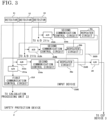
FIG. 2] FIG. 2 is a schematic structure view of a safety protection system backup device according toembodiment 2. - [
FIG. 3] FIG. 3 is a schematic structure view of a safety protection system backup device according toembodiment 3. - [
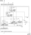
FIG. 4] FIG. 4 is a schematic structure view of a safety protection system backup device according to embodiment 4. - [
FIG. 5] FIG. 5 is a hardware configuration diagram of a safety protection logic according toembodiments 1 to 4. - Hereinafter, preferred embodiments of a safety protection system backup device according to the present disclosure will be described with reference to the drawings. The same or corresponding things and parts are denoted by the same reference characters, and the detailed description thereof is omitted. Also, in the following embodiments, components denoted by the same reference characters will not be described repeatedly.
-
FIG. 1 is a schematic structure view of the safety protection system backup device of the present embodiment. A case where the present embodiment is applied to a nuclear power plant will be described, but the present embodiment is not limited thereto. Adetector 1 monitors the state of a nuclear power plant, and transmits a detection signal to asafety protection device 2 which is a protection-system facility. The transmitted detection signal is inputted to aninput device 21 of thesafety protection device 2, and is electrically distributed in theinput device 21. One of the distributed signals is inputted to an analog/digital (A/D)conversion circuit 211 of thesafety protection device 2 and another thereof is inputted to an A/D conversion circuit 212 for aCCF device 3. - The detection signal is converted to a digital signal by the A/
D conversion circuit 211, and the digital signal is transmitted to acalculation processing unit 22 via a firstcommunication control circuit 213 of thesafety protection device 2. The transmitted digital signal is received by a thirdcommunication control circuit 221 which is an input at thecalculation processing unit 22, and is used, by asafety protection logic 222 implemented as execution of a previously designed protection logic (hereinafter, referred to as application software) by a microprocessor or a FPGA, to generate an operation command signal of the protection-system facility to a safety-system local component 4. The operation command signal, generated by thesafety protection logic 222, to the safety-system local component 4 is transmitted to anoutput device 23 via a fifthcommunication control circuit 223 which is an output at thecalculation processing unit 22. Here, the function of application software includes four analog arithmetic operations, in addition to a logical operation. - In the
output device 23, the operation command signal transmitted from the fifthcommunication control circuit 223 is received by a seventhcommunication control circuit 231 and then is converted to an analog signal by a digital/analog (D/A)conversion circuit 232, and the analog signal is transmitted to a hardware (H/W)circuit 236 which is a final output end. The H/W circuit executes priority processing on the inputted signal. Examples of the H/W circuit include an OR circuit, an AND circuit, an ON priority circuit, and an OFF priority circuit. However, the H/W circuit is not limited thereto. - On the other hand, the digital signal inputted to the A/
D conversion circuit 212 is transmitted to a secondcommunication control circuit 214 for theCCF device 3. - The A/
D conversion circuit 211 and the A/D conversion circuit 212 are respectively composed of and implemented with circuits or devices (parts) different from each other. Similarly, the firstcommunication control circuit 213 and the secondcommunication control circuit 214 are also respectively composed of and implemented with circuits or parts different from each other. - The second
communication control circuit 214 transmits the inputted digital signal to a fourthcommunication control circuit 311 connected to acalculation processing unit 31 of theCCF device 3 in the same manner as for thecalculation processing unit 22. The transmitted digital signal is received by the fourthcommunication control circuit 311, and then is used, by thesafety protection logic 312 configured by a microprocessor or a field-programmable gate array (FPGA) in which application software is implemented, to generate an operation request signal to the safety-system local component 4. - Here, in order to ensure diversity, the following is applied to each component:
- (1) As a communication protocol between the second
communication control circuit 214 and the fourthcommunication control circuit 311, a communication protocol different from a communication protocol to be applied between the firstcommunication control circuit 213 and the thirdcommunication control circuit 221 is applied. - (2) The
calculation processing unit 31 and thecalculation processing unit 22 respectively execute similar digital signal processings by different circuits. For example, as a microprocessor of thecalculation processing unit 31, a device different from a microprocessor of thecalculation processing unit 22 is applied, or a FPGA is used in thecalculation processing unit 31. - (3) The
safety protection logic 312 and thesafety protection logic 222 are respectively designed on the basis of different ideas for similar digital signal processings. For example, in a case where microprocessors are used in thecalculation processing unit 31 and thecalculation processing unit 22, design concepts of application software to be implemented are made different, and the microprocessors are designed by different designers so as not to make determination on the basis of the same logical configuration. In a case where a FPGA is used in thecalculation processing unit 31, the FPGA is programmed by a different designer so that processing similar to the digital signal processing by the microprocessor in thecalculation processing unit 22 has a logical configuration based on a different design concept. - (4) The
CCF device 3 and thesafety protection device 2 are designed by different designers in different departments so as to have different design concepts and provide protection on the basis of different logical configurations, respectively. - The operation request signal, generated by the
safety protection logic 312, to the safety-system local component 4 is transmitted to theoutput device 23 of thesafety protection device 2 from a sixthcommunication control circuit 313 which is an output at thecalculation processing unit 31. The transmitted operation request signal is received by an eighthcommunication control circuit 235 for theCCF device 3 and then is converted to an analog signal by a D/A conversion circuit 234 for theCCF device 3, and then the analog signal is outputted to the H/W circuit 236. - The D/
A conversion circuit 232 and the D/A conversion circuit 234 are respectively composed of and implemented with circuits or devices (parts) different from each other. Similarly, the seventhcommunication control circuit 231 and the eighthcommunication control circuit 235 are respectively composed of circuits or parts different from each other. Further, as a communication protocol between the sixthcommunication control circuit 313 and the eighthcommunication control circuit 235, a communication protocol different from a communication protocol between the fifthcommunication control circuit 223 and the seventhcommunication control circuit 231 is applied. - The safety protection system backup device is configured as described above, whereby the input device and the output device can be shared by the safety protection equipment and the CCF device. Thus, an input device and an output device exclusive to the CCF device need not be provided, and increase in the number of the detectors and the safety-system local components can also be dealt with without increasing the scale of the CCF device.
- In the configuration of
embodiment 1, a photoelectric (E/O)conversion circuit 24 which converts to an optical signal an electric signal transmitted from the secondcommunication control circuit 214 of thesafety protection device 2, and an O/E conversion circuit 32 which converts to an electric signal the optical signal received by the CCF device, are applied. - Similarly, an E/
O conversion circuit 33 which converts to an optical signal an output signal of the sixthcommunication control circuit 313 of theCCF device 3, and an O/E conversion circuit 25 which converts to an electric signal the signal received by thesafety protection device 2, are applied. - Thus, optical signals are transmitted and received between the
safety protection device 2 and theCCF device 3, whereby, in a case where an electric fault or the like has occurred in theCCF device 3, the influence of the failure is prevented from spreading to thesafety protection device 2. Further, since signals are transmitted through optical cables, a transmission distance can be extended as compared to a case where electric signals are used, and a constraint condition for an installation place of theCCF device 3 can be relaxed. - As described above, in the configuration of
embodiment 2, the CCF device is connected to the input device and the output device through the optical cables, whereby an electric fault in the CCF device can be prevented from influencing the safety protection system backup device, and a separation device need not be provided. - As shown in
FIG. 3 , in the configuration ofembodiment 1 orembodiment 2, detection signals from a plurality ofdetectors safety protection device 2 which is a protection-system facility. The transmitted detection signals are inputted to inputdevices safety protection device 2, and are electrically distributed in theinput devices D conversion circuits safety protection device 2 and the signals distributed to another side are inputted to A/D conversion circuits CCF device 3. Outputs from the A/D conversion circuits repeater circuits communication control circuits repeater circuits CCF device 3 via an E/O conversion circuit 24. With such a configuration, the detection signals from the plurality ofdetectors CCF device 3 without increasing the number of transmission lines. In the present embodiment, an example in which signals from the three detectors are inputted to the three input devices is shown, but the number of the detectors and the number of the input devices are not limited thereto. - As shown in
FIG. 4 , the detection signals transmitted from thedetectors input devices input devices D conversion circuits safety protection device 2 and the signals distributed to another side are inputted to the A/D conversion circuit 212 for theCCF device 3 in one input device (e.g., input device 2101). An output from the A/D conversion circuit 212 is inputted to arepeater circuit 26 via the secondcommunication control circuit 214. The signal amplified by therepeater circuit 26 is transmitted to theCCF device 3 via the E/O conversion circuit 24. Thus, the A/D conversion circuits for theCCF device 3 in the twoinput devices - One example of hardware of the
safety protection logics FIG. 5 . As described above, thesafety protection logics microprocessor 50 and astorage device 60. Although not shown, astorage device 60 includes a volatile storage device such as a random access memory, and a nonvolatile auxiliary storage device such as a flash memory. Thestorage device 60 may include an auxiliary storage device such as a hard disk, instead of a flash memory. Themicroprocessor 50 executes application software inputted from thestorage device 60. In this case, the program is inputted to themicroprocessor 50 via the volatile storage device from the auxiliary storage device. Themicroprocessor 50 may output data such as a calculation result to the volatile storage device of thestorage device 60, or store such data into the auxiliary storage device via the volatile storage device. As hardware of thesafety protection logic 312, a FPGA may be used instead of the microprocessor, as described above. - Although the disclosure is described above in terms of various exemplary embodiments and implementations, it should be understood that the various features, aspects, and functionality described in one or more of the individual embodiments are not limited in their applicability to the particular embodiment with which they are described, but instead can be applied, alone or in various combinations to one or more of the embodiments of the disclosure.
- It is therefore understood that numerous modifications which have not been exemplified can be devised without departing from the scope of the present disclosure. For example, at least one of the constituent components may be modified, added, or eliminated. At least one of the constituent components mentioned in at least one of the preferred embodiments may be selected and combined with the constituent components mentioned in another preferred embodiment.
-
- 1, 11, 12, 13 detector
- 2 safety protection device
- 3 CCF device
- 4 safety-system local component
- 21, 2101, 2102, 2103 input device
- 22 calculation processing unit
- 23 output device
- 24 E/O conversion circuit
- 25 O/E conversion circuit
- 26, 26a, 26b, 26c repeater circuit
- 31 calculation processing unit
- 32 O/E conversion circuit
- 33 E/O conversion circuit
- 50 microprocessor
- 60 storage device
- 211, 211a, 211b, 211c, 212, 212a, 212b, 212c A/D conversion circuit
- 213 first communication control circuit
- 214, 214a, 214b, 214c second communication control circuit
- 221 third communication control circuit
- 222 safety protection logic
- 223 fifth communication control circuit
- 231 seventh communication control circuit
- 232, 234 D/A conversion circuit
- 235 eighth communication control circuit
- 236 H/W circuit
- 311 fourth communication control circuit
- 312 safety protection logic
- 313 sixth communication control circuit
Claims (4)
- A safety protection system backup device which detects a state of a plant, and which, if an abnormality is found, issues an instruction to a safety-system local component according to an output of a first safety protection logic in a safety protection device and, if a common cause failure is found in the safety protection device, issues an instruction to the safety-system local component according to an output of a second safety protection logic in a CCF device, the safety protection system backup device comprising:a detector which detects a state of the plant;first and second analog/digital conversion circuits which are disposed in an input device of the safety protection device and perform digital conversion on an output of the detector;a first communication control circuit which is disposed in the input device and transmits to a calculation processing unit a signal outputted from the first analog/digital conversion circuit;a second communication control circuit which is disposed in the input device and transmits to the CCF device a signal outputted from the second analog/digital conversion circuit;a third communication control circuit which is disposed in a first calculation processing unit of the safety protection device, receives an output of the first communication control circuit, and transmits the output to the first safety protection logic of the calculation processing unit;a fourth communication control circuit which receives an output of the second communication control circuit and transmits the output to the second safety protection logic disposed in a second calculation processing unit of the CCF device;a fifth communication control circuit which is disposed in the first calculation processing unit and transmits an output of the first safety protection logic;a sixth communication control circuit which is disposed in the second calculation processing unit and transmits an output of the second safety protection logic;a seventh communication control circuit which receives a signal transmitted from the fifth communication control circuit and is disposed in an output device region of the safety protection device;an eighth communication control circuit which receives a signal transmitted from the sixth communication control circuit and is disposed in the output device region;a first digital/analog conversion circuit which is disposed in the output device region and performs analog conversion on a signal of the seventh communication control circuit;a second digital/analog conversion circuit which is disposed in the output device region and performs analog conversion on a signal of the eighth communication control circuit; anda hardware circuit to which a signal of the first or second digital/analog conversion circuit is inputted and which performs output to the safety-system local component, whereinthe first safety protection logic and the second safety protection logic execute digital signal processings based on logical configurations different from each other,the first analog/digital conversion circuit and the second analog/digital conversion circuit are composed of circuits or parts different from each other,the first digital/analog conversion circuit and the second digital/analog conversion circuit are composed of circuits or parts different from each other,a communication protocol between the first communication control circuit and the third communication control circuit is different from a communication protocol between the second communication control circuit and the fourth communication control circuit, anda communication protocol between the fifth communication control circuit and the seventh communication control circuit is different from a communication protocol between the sixth communication control circuit and the eighth communication control circuit.
- The safety protection system backup device according to claim 1, whereina first photoelectric conversion circuit is connected to a stage subsequent to the second communication control circuit,a second photoelectric conversion circuit is connected to a stage preceding the fourth communication control circuit,the first photoelectric conversion circuit and the second photoelectric conversion circuit are connected by an optical fiber cable,a third photoelectric conversion circuit is connected to a stage subsequent to the sixth communication control circuit,a fourth photoelectric conversion circuit is connected to a stage preceding the eighth communication control circuit, andthe third photoelectric conversion circuit and the fourth photoelectric conversion circuit are connected by an optical fiber cable.
- The safety protection system backup device according to claim 1 or 2, wherein
in a case where outputs of a plurality of the detectors are subjected to digital conversion by a plurality of the second analog/digital conversion circuits disposed in a plurality of the input devices and then are transmitted to the CCF device via a plurality of the second communication control circuits, outputs from the plurality of second communication control circuits are transmitted via repeater circuits. - The safety protection system backup device according to claim 1 or 2, wherein
in a case where outputs of a plurality of the detectors are inputted to a plurality of the input devices and then are transmitted to the CCF device, the outputs of the plurality of detectors are converted by the second analog/digital conversion circuit disposed in one of the input devices.
Applications Claiming Priority (1)
| Application Number | Priority Date | Filing Date | Title |
|---|---|---|---|
| PCT/JP2022/005280 WO2023152853A1 (en) | 2022-02-10 | 2022-02-10 | Safety protection system backup device |
Publications (3)
| Publication Number | Publication Date |
|---|---|
| EP4478136A1 true EP4478136A1 (en) | 2024-12-18 |
| EP4478136A4 EP4478136A4 (en) | 2025-03-12 |
| EP4478136B1 EP4478136B1 (en) | 2025-09-24 |
Family
ID=87563879
Family Applications (1)
| Application Number | Title | Priority Date | Filing Date |
|---|---|---|---|
| EP22925874.4A Active EP4478136B1 (en) | 2022-02-10 | 2022-02-10 | Safety protection system backup device |
Country Status (6)
| Country | Link |
|---|---|
| US (1) | US20250155887A1 (en) |
| EP (1) | EP4478136B1 (en) |
| JP (1) | JP7630664B2 (en) |
| CA (1) | CA3241758A1 (en) |
| UA (1) | UA130689C2 (en) |
| WO (1) | WO2023152853A1 (en) |
Family Cites Families (10)
| Publication number | Priority date | Publication date | Assignee | Title |
|---|---|---|---|---|
| KR100408493B1 (en) | 2001-05-07 | 2003-12-06 | 한국전력기술 주식회사 | System for digital reactor protecting to prevent common mode failures and control method of the same |
| JP4371856B2 (en) * | 2004-03-04 | 2009-11-25 | 株式会社東芝 | Safety protection instrumentation system and its handling method |
| JP2011191855A (en) * | 2010-03-12 | 2011-09-29 | Hitachi-Ge Nuclear Energy Ltd | Digital safety protection system |
| JP5675208B2 (en) * | 2010-08-06 | 2015-02-25 | 三菱重工業株式会社 | Nuclear facility control system |
| JP5701033B2 (en) | 2010-12-09 | 2015-04-15 | 三菱重工業株式会社 | Reactor shutdown device |
| CN103400623A (en) | 2013-07-30 | 2013-11-20 | 中广核工程有限公司 | Protection method and system for digitalized instrument control diversity of nuclear power station |
| JP6721423B2 (en) * | 2016-06-14 | 2020-07-15 | 株式会社日立製作所 | App logic and its verification method |
| JP2018101241A (en) * | 2016-12-20 | 2018-06-28 | 株式会社日立製作所 | Processing device |
| JP6847755B2 (en) | 2017-04-28 | 2021-03-24 | 三菱重工業株式会社 | Plant monitoring and control device |
| WO2020090034A1 (en) * | 2018-10-31 | 2020-05-07 | 株式会社日立製作所 | Processing device |
-
2022
- 2022-02-10 CA CA3241758A patent/CA3241758A1/en active Pending
- 2022-02-10 WO PCT/JP2022/005280 patent/WO2023152853A1/en not_active Ceased
- 2022-02-10 UA UAA202403764A patent/UA130689C2/en unknown
- 2022-02-10 US US18/720,314 patent/US20250155887A1/en active Pending
- 2022-02-10 EP EP22925874.4A patent/EP4478136B1/en active Active
- 2022-02-10 JP JP2023579941A patent/JP7630664B2/en active Active
Also Published As
| Publication number | Publication date |
|---|---|
| JPWO2023152853A1 (en) | 2023-08-17 |
| JP7630664B2 (en) | 2025-02-17 |
| CA3241758A1 (en) | 2023-08-17 |
| UA130689C2 (en) | 2026-04-15 |
| EP4478136A4 (en) | 2025-03-12 |
| EP4478136B1 (en) | 2025-09-24 |
| WO2023152853A1 (en) | 2023-08-17 |
| US20250155887A1 (en) | 2025-05-15 |
Similar Documents
| Publication | Publication Date | Title |
|---|---|---|
| CN105575448B (en) | Nuclear power plant reactor protects system and method for controlling security therein | |
| KR101552852B1 (en) | Triple redundant digital protective relay and operating method thereof | |
| US9997265B2 (en) | Safety system for a nuclear power plant and method for operating the same | |
| KR100980043B1 (en) | Power plant protection system and method using FPA | |
| US11225867B2 (en) | Breaker auto-synchronizer | |
| JP2018064416A (en) | Two parallel line transmission line protection system | |
| KR100848881B1 (en) | Digital reactor protection system | |
| KR101903073B1 (en) | Method and Apparatus for prevention of Reactor Trip in a Loss of one Reactor Coolant Pump | |
| KR101681978B1 (en) | Reactor Protection System Having Different Kind of Control Apparatus | |
| KR20010076542A (en) | Digital Plant Protection System in Nuclear Power Plant | |
| EP4478136A1 (en) | Safety protection system backup device | |
| KR101042030B1 (en) | Power plant protection system integrating comparative and simultaneous logic | |
| KR101831398B1 (en) | Diverse Protection System | |
| KR20160086082A (en) | Protection system for nuclear plant and Method of operating protection system for nuclear plant | |
| WO2023042344A1 (en) | Protection and control system | |
| KR102918576B1 (en) | Method and system for preventing power system failure by separating circuit | |
| KR200347633Y1 (en) | Hardware structure of intelligent electronic device for fault detection and selective auto-reclosure | |
| KR102110378B1 (en) | Differential protective apparatus and method to prevent malfunction by digital protection relay's internal computation error | |
| Kumar et al. | A review of defences against common cause failures in reactor protection systems | |
| JP5555040B2 (en) | Distribution line protection relay unit setting value support system | |
| KR102918581B1 (en) | Method and system for preventing non-operation of protection relay | |
| KR102673587B1 (en) | System and Method for preliminary integrated control monitoring to relieve vulnerability of digital substation | |
| KR102945258B1 (en) | Method and system for power stabilizating with improved detection of overcurrent protection type failures | |
| US20190207377A1 (en) | Systems and methods for script implemented logic for trigger for converting electromechanical relay outputs into fault indication for automatic restoration application | |
| US20240305090A1 (en) | Method and system for protecting an electrical distribution network comprising at least two sources of electrical energy |
Legal Events
| Date | Code | Title | Description |
|---|---|---|---|
| STAA | Information on the status of an ep patent application or granted ep patent |
Free format text: STATUS: THE INTERNATIONAL PUBLICATION HAS BEEN MADE |
|
| PUAI | Public reference made under article 153(3) epc to a published international application that has entered the european phase |
Free format text: ORIGINAL CODE: 0009012 |
|
| STAA | Information on the status of an ep patent application or granted ep patent |
Free format text: STATUS: REQUEST FOR EXAMINATION WAS MADE |
|
| 17P | Request for examination filed |
Effective date: 20240620 |
|
| AK | Designated contracting states |
Kind code of ref document: A1 Designated state(s): AL AT BE BG CH CY CZ DE DK EE ES FI FR GB GR HR HU IE IS IT LI LT LU LV MC MK MT NL NO PL PT RO RS SE SI SK SM TR |
|
| A4 | Supplementary search report drawn up and despatched |
Effective date: 20250207 |
|
| RIC1 | Information provided on ipc code assigned before grant |
Ipc: G21D 3/06 20060101ALI20250203BHEP Ipc: G05B 9/02 20060101AFI20250203BHEP |
|
| DAV | Request for validation of the european patent (deleted) | ||
| DAX | Request for extension of the european patent (deleted) | ||
| GRAP | Despatch of communication of intention to grant a patent |
Free format text: ORIGINAL CODE: EPIDOSNIGR1 |
|
| STAA | Information on the status of an ep patent application or granted ep patent |
Free format text: STATUS: GRANT OF PATENT IS INTENDED |
|
| RIC1 | Information provided on ipc code assigned before grant |
Ipc: G21D 3/06 20060101ALI20250528BHEP Ipc: G05B 9/02 20060101AFI20250528BHEP |
|
| INTG | Intention to grant announced |
Effective date: 20250616 |
|
| RIN1 | Information on inventor provided before grant (corrected) |
Inventor name: OKUDA, SUSUMU |
|
| GRAS | Grant fee paid |
Free format text: ORIGINAL CODE: EPIDOSNIGR3 |
|
| GRAA | (expected) grant |
Free format text: ORIGINAL CODE: 0009210 |
|
| STAA | Information on the status of an ep patent application or granted ep patent |
Free format text: STATUS: THE PATENT HAS BEEN GRANTED |
|
| AK | Designated contracting states |
Kind code of ref document: B1 Designated state(s): AL AT BE BG CH CY CZ DE DK EE ES FI FR GB GR HR HU IE IS IT LI LT LU LV MC MK MT NL NO PL PT RO RS SE SI SK SM TR |
|
| REG | Reference to a national code |
Ref country code: GB Ref legal event code: FG4D |
|
| REG | Reference to a national code |
Ref country code: CH Ref legal event code: EP |
|
| REG | Reference to a national code |
Ref country code: DE Ref legal event code: R096 Ref document number: 602022022108 Country of ref document: DE |
|
| REG | Reference to a national code |
Ref country code: IE Ref legal event code: FG4D |
|
| PG25 | Lapsed in a contracting state [announced via postgrant information from national office to epo] |
Ref country code: NO Free format text: LAPSE BECAUSE OF FAILURE TO SUBMIT A TRANSLATION OF THE DESCRIPTION OR TO PAY THE FEE WITHIN THE PRESCRIBED TIME-LIMIT Effective date: 20251224 |
|
| REG | Reference to a national code |
Ref country code: LT Ref legal event code: MG9D |
|
| PG25 | Lapsed in a contracting state [announced via postgrant information from national office to epo] |
Ref country code: FI Free format text: LAPSE BECAUSE OF FAILURE TO SUBMIT A TRANSLATION OF THE DESCRIPTION OR TO PAY THE FEE WITHIN THE PRESCRIBED TIME-LIMIT Effective date: 20250924 |
|
| PG25 | Lapsed in a contracting state [announced via postgrant information from national office to epo] |
Ref country code: HR Free format text: LAPSE BECAUSE OF FAILURE TO SUBMIT A TRANSLATION OF THE DESCRIPTION OR TO PAY THE FEE WITHIN THE PRESCRIBED TIME-LIMIT Effective date: 20250924 |
|
| PGFP | Annual fee paid to national office [announced via postgrant information from national office to epo] |
Ref country code: FR Payment date: 20251231 Year of fee payment: 5 |
|
| PG25 | Lapsed in a contracting state [announced via postgrant information from national office to epo] |
Ref country code: GR Free format text: LAPSE BECAUSE OF FAILURE TO SUBMIT A TRANSLATION OF THE DESCRIPTION OR TO PAY THE FEE WITHIN THE PRESCRIBED TIME-LIMIT Effective date: 20251225 |
|
| PG25 | Lapsed in a contracting state [announced via postgrant information from national office to epo] |
Ref country code: SE Free format text: LAPSE BECAUSE OF FAILURE TO SUBMIT A TRANSLATION OF THE DESCRIPTION OR TO PAY THE FEE WITHIN THE PRESCRIBED TIME-LIMIT Effective date: 20250924 |
|
| PG25 | Lapsed in a contracting state [announced via postgrant information from national office to epo] |
Ref country code: LV Free format text: LAPSE BECAUSE OF FAILURE TO SUBMIT A TRANSLATION OF THE DESCRIPTION OR TO PAY THE FEE WITHIN THE PRESCRIBED TIME-LIMIT Effective date: 20250924 |
|
| PG25 | Lapsed in a contracting state [announced via postgrant information from national office to epo] |
Ref country code: BG Free format text: LAPSE BECAUSE OF FAILURE TO SUBMIT A TRANSLATION OF THE DESCRIPTION OR TO PAY THE FEE WITHIN THE PRESCRIBED TIME-LIMIT Effective date: 20250924 |
|
| PG25 | Lapsed in a contracting state [announced via postgrant information from national office to epo] |
Ref country code: RS Free format text: LAPSE BECAUSE OF FAILURE TO SUBMIT A TRANSLATION OF THE DESCRIPTION OR TO PAY THE FEE WITHIN THE PRESCRIBED TIME-LIMIT Effective date: 20251224 |
|
| REG | Reference to a national code |
Ref country code: NL Ref legal event code: MP Effective date: 20250924 |
|
| PG25 | Lapsed in a contracting state [announced via postgrant information from national office to epo] |
Ref country code: NL Free format text: LAPSE BECAUSE OF FAILURE TO SUBMIT A TRANSLATION OF THE DESCRIPTION OR TO PAY THE FEE WITHIN THE PRESCRIBED TIME-LIMIT Effective date: 20250924 |
|
| REG | Reference to a national code |
Ref country code: AT Ref legal event code: MK05 Ref document number: 1840792 Country of ref document: AT Kind code of ref document: T Effective date: 20250924 |
|
| PG25 | Lapsed in a contracting state [announced via postgrant information from national office to epo] |
Ref country code: SM Free format text: LAPSE BECAUSE OF FAILURE TO SUBMIT A TRANSLATION OF THE DESCRIPTION OR TO PAY THE FEE WITHIN THE PRESCRIBED TIME-LIMIT Effective date: 20250924 |
|
| PGFP | Annual fee paid to national office [announced via postgrant information from national office to epo] |
Ref country code: GB Payment date: 20260106 Year of fee payment: 5 |
|
| PG25 | Lapsed in a contracting state [announced via postgrant information from national office to epo] |
Ref country code: ES Free format text: LAPSE BECAUSE OF FAILURE TO SUBMIT A TRANSLATION OF THE DESCRIPTION OR TO PAY THE FEE WITHIN THE PRESCRIBED TIME-LIMIT Effective date: 20250924 |
|
| PG25 | Lapsed in a contracting state [announced via postgrant information from national office to epo] |
Ref country code: AT Free format text: LAPSE BECAUSE OF FAILURE TO SUBMIT A TRANSLATION OF THE DESCRIPTION OR TO PAY THE FEE WITHIN THE PRESCRIBED TIME-LIMIT Effective date: 20250924 |
|
| PG25 | Lapsed in a contracting state [announced via postgrant information from national office to epo] |
Ref country code: IT Free format text: LAPSE BECAUSE OF FAILURE TO SUBMIT A TRANSLATION OF THE DESCRIPTION OR TO PAY THE FEE WITHIN THE PRESCRIBED TIME-LIMIT Effective date: 20250924 |
|
| PG25 | Lapsed in a contracting state [announced via postgrant information from national office to epo] |
Ref country code: IS Free format text: LAPSE BECAUSE OF FAILURE TO SUBMIT A TRANSLATION OF THE DESCRIPTION OR TO PAY THE FEE WITHIN THE PRESCRIBED TIME-LIMIT Effective date: 20260124 |
|
| PG25 | Lapsed in a contracting state [announced via postgrant information from national office to epo] |
Ref country code: CZ Free format text: LAPSE BECAUSE OF FAILURE TO SUBMIT A TRANSLATION OF THE DESCRIPTION OR TO PAY THE FEE WITHIN THE PRESCRIBED TIME-LIMIT Effective date: 20250924 Ref country code: PT Free format text: LAPSE BECAUSE OF FAILURE TO SUBMIT A TRANSLATION OF THE DESCRIPTION OR TO PAY THE FEE WITHIN THE PRESCRIBED TIME-LIMIT Effective date: 20260126 |
|
| PG25 | Lapsed in a contracting state [announced via postgrant information from national office to epo] |
Ref country code: PL Free format text: LAPSE BECAUSE OF FAILURE TO SUBMIT A TRANSLATION OF THE DESCRIPTION OR TO PAY THE FEE WITHIN THE PRESCRIBED TIME-LIMIT Effective date: 20250924 |
|
| PG25 | Lapsed in a contracting state [announced via postgrant information from national office to epo] |
Ref country code: EE Free format text: LAPSE BECAUSE OF FAILURE TO SUBMIT A TRANSLATION OF THE DESCRIPTION OR TO PAY THE FEE WITHIN THE PRESCRIBED TIME-LIMIT Effective date: 20250924 Ref country code: SK Free format text: LAPSE BECAUSE OF FAILURE TO SUBMIT A TRANSLATION OF THE DESCRIPTION OR TO PAY THE FEE WITHIN THE PRESCRIBED TIME-LIMIT Effective date: 20250924 |