EP4478122A1 - Backlight structure and display device - Google Patents
Backlight structure and display device Download PDFInfo
- Publication number
- EP4478122A1 EP4478122A1 EP23867519.3A EP23867519A EP4478122A1 EP 4478122 A1 EP4478122 A1 EP 4478122A1 EP 23867519 A EP23867519 A EP 23867519A EP 4478122 A1 EP4478122 A1 EP 4478122A1
- Authority
- EP
- European Patent Office
- Prior art keywords
- light
- emitting units
- substrate
- region
- emitting
- Prior art date
- Legal status (The legal status is an assumption and is not a legal conclusion. Google has not performed a legal analysis and makes no representation as to the accuracy of the status listed.)
- Pending
Links
Images











Classifications
-
- G—PHYSICS
- G02—OPTICS
- G02F—OPTICAL DEVICES OR ARRANGEMENTS FOR THE CONTROL OF LIGHT BY MODIFICATION OF THE OPTICAL PROPERTIES OF THE MEDIA OF THE ELEMENTS INVOLVED THEREIN; NON-LINEAR OPTICS; FREQUENCY-CHANGING OF LIGHT; OPTICAL LOGIC ELEMENTS; OPTICAL ANALOGUE/DIGITAL CONVERTERS
- G02F1/00—Devices or arrangements for the control of the intensity, colour, phase, polarisation or direction of light arriving from an independent light source, e.g. switching, gating or modulating; Non-linear optics
- G02F1/01—Devices or arrangements for the control of the intensity, colour, phase, polarisation or direction of light arriving from an independent light source, e.g. switching, gating or modulating; Non-linear optics for the control of the intensity, phase, polarisation or colour
- G02F1/13—Devices or arrangements for the control of the intensity, colour, phase, polarisation or direction of light arriving from an independent light source, e.g. switching, gating or modulating; Non-linear optics for the control of the intensity, phase, polarisation or colour based on liquid crystals, e.g. single liquid crystal display cells
- G02F1/133—Constructional arrangements; Operation of liquid crystal cells; Circuit arrangements
- G02F1/1333—Constructional arrangements; Manufacturing methods
- G02F1/1335—Structural association of cells with optical devices, e.g. polarisers or reflectors
- G02F1/1336—Illuminating devices
-
- G—PHYSICS
- G02—OPTICS
- G02F—OPTICAL DEVICES OR ARRANGEMENTS FOR THE CONTROL OF LIGHT BY MODIFICATION OF THE OPTICAL PROPERTIES OF THE MEDIA OF THE ELEMENTS INVOLVED THEREIN; NON-LINEAR OPTICS; FREQUENCY-CHANGING OF LIGHT; OPTICAL LOGIC ELEMENTS; OPTICAL ANALOGUE/DIGITAL CONVERTERS
- G02F1/00—Devices or arrangements for the control of the intensity, colour, phase, polarisation or direction of light arriving from an independent light source, e.g. switching, gating or modulating; Non-linear optics
- G02F1/01—Devices or arrangements for the control of the intensity, colour, phase, polarisation or direction of light arriving from an independent light source, e.g. switching, gating or modulating; Non-linear optics for the control of the intensity, phase, polarisation or colour
- G02F1/13—Devices or arrangements for the control of the intensity, colour, phase, polarisation or direction of light arriving from an independent light source, e.g. switching, gating or modulating; Non-linear optics for the control of the intensity, phase, polarisation or colour based on liquid crystals, e.g. single liquid crystal display cells
- G02F1/133—Constructional arrangements; Operation of liquid crystal cells; Circuit arrangements
- G02F1/1333—Constructional arrangements; Manufacturing methods
- G02F1/1335—Structural association of cells with optical devices, e.g. polarisers or reflectors
- G02F1/1336—Illuminating devices
- G02F1/133602—Direct backlight
- G02F1/133603—Direct backlight with LEDs
-
- G—PHYSICS
- G02—OPTICS
- G02F—OPTICAL DEVICES OR ARRANGEMENTS FOR THE CONTROL OF LIGHT BY MODIFICATION OF THE OPTICAL PROPERTIES OF THE MEDIA OF THE ELEMENTS INVOLVED THEREIN; NON-LINEAR OPTICS; FREQUENCY-CHANGING OF LIGHT; OPTICAL LOGIC ELEMENTS; OPTICAL ANALOGUE/DIGITAL CONVERTERS
- G02F1/00—Devices or arrangements for the control of the intensity, colour, phase, polarisation or direction of light arriving from an independent light source, e.g. switching, gating or modulating; Non-linear optics
- G02F1/01—Devices or arrangements for the control of the intensity, colour, phase, polarisation or direction of light arriving from an independent light source, e.g. switching, gating or modulating; Non-linear optics for the control of the intensity, phase, polarisation or colour
- G02F1/13—Devices or arrangements for the control of the intensity, colour, phase, polarisation or direction of light arriving from an independent light source, e.g. switching, gating or modulating; Non-linear optics for the control of the intensity, phase, polarisation or colour based on liquid crystals, e.g. single liquid crystal display cells
- G02F1/133—Constructional arrangements; Operation of liquid crystal cells; Circuit arrangements
- G02F1/1333—Constructional arrangements; Manufacturing methods
- G02F1/1335—Structural association of cells with optical devices, e.g. polarisers or reflectors
- G02F1/1336—Illuminating devices
- G02F1/133601—Illuminating devices for spatial active dimming
-
- G—PHYSICS
- G02—OPTICS
- G02F—OPTICAL DEVICES OR ARRANGEMENTS FOR THE CONTROL OF LIGHT BY MODIFICATION OF THE OPTICAL PROPERTIES OF THE MEDIA OF THE ELEMENTS INVOLVED THEREIN; NON-LINEAR OPTICS; FREQUENCY-CHANGING OF LIGHT; OPTICAL LOGIC ELEMENTS; OPTICAL ANALOGUE/DIGITAL CONVERTERS
- G02F1/00—Devices or arrangements for the control of the intensity, colour, phase, polarisation or direction of light arriving from an independent light source, e.g. switching, gating or modulating; Non-linear optics
- G02F1/01—Devices or arrangements for the control of the intensity, colour, phase, polarisation or direction of light arriving from an independent light source, e.g. switching, gating or modulating; Non-linear optics for the control of the intensity, phase, polarisation or colour
- G02F1/13—Devices or arrangements for the control of the intensity, colour, phase, polarisation or direction of light arriving from an independent light source, e.g. switching, gating or modulating; Non-linear optics for the control of the intensity, phase, polarisation or colour based on liquid crystals, e.g. single liquid crystal display cells
- G02F1/133—Constructional arrangements; Operation of liquid crystal cells; Circuit arrangements
- G02F1/1333—Constructional arrangements; Manufacturing methods
- G02F1/1335—Structural association of cells with optical devices, e.g. polarisers or reflectors
- G02F1/1336—Illuminating devices
- G02F1/133602—Direct backlight
- G02F1/133606—Direct backlight including a specially adapted diffusing, scattering or light controlling members
-
- G—PHYSICS
- G02—OPTICS
- G02F—OPTICAL DEVICES OR ARRANGEMENTS FOR THE CONTROL OF LIGHT BY MODIFICATION OF THE OPTICAL PROPERTIES OF THE MEDIA OF THE ELEMENTS INVOLVED THEREIN; NON-LINEAR OPTICS; FREQUENCY-CHANGING OF LIGHT; OPTICAL LOGIC ELEMENTS; OPTICAL ANALOGUE/DIGITAL CONVERTERS
- G02F1/00—Devices or arrangements for the control of the intensity, colour, phase, polarisation or direction of light arriving from an independent light source, e.g. switching, gating or modulating; Non-linear optics
- G02F1/01—Devices or arrangements for the control of the intensity, colour, phase, polarisation or direction of light arriving from an independent light source, e.g. switching, gating or modulating; Non-linear optics for the control of the intensity, phase, polarisation or colour
- G02F1/13—Devices or arrangements for the control of the intensity, colour, phase, polarisation or direction of light arriving from an independent light source, e.g. switching, gating or modulating; Non-linear optics for the control of the intensity, phase, polarisation or colour based on liquid crystals, e.g. single liquid crystal display cells
- G02F1/133—Constructional arrangements; Operation of liquid crystal cells; Circuit arrangements
- G02F1/1333—Constructional arrangements; Manufacturing methods
- G02F1/1335—Structural association of cells with optical devices, e.g. polarisers or reflectors
- G02F1/1336—Illuminating devices
- G02F1/133602—Direct backlight
- G02F1/133606—Direct backlight including a specially adapted diffusing, scattering or light controlling members
- G02F1/133607—Direct backlight including a specially adapted diffusing, scattering or light controlling members the light controlling member including light directing or refracting elements, e.g. prisms or lenses
-
- G—PHYSICS
- G02—OPTICS
- G02F—OPTICAL DEVICES OR ARRANGEMENTS FOR THE CONTROL OF LIGHT BY MODIFICATION OF THE OPTICAL PROPERTIES OF THE MEDIA OF THE ELEMENTS INVOLVED THEREIN; NON-LINEAR OPTICS; FREQUENCY-CHANGING OF LIGHT; OPTICAL LOGIC ELEMENTS; OPTICAL ANALOGUE/DIGITAL CONVERTERS
- G02F1/00—Devices or arrangements for the control of the intensity, colour, phase, polarisation or direction of light arriving from an independent light source, e.g. switching, gating or modulating; Non-linear optics
- G02F1/01—Devices or arrangements for the control of the intensity, colour, phase, polarisation or direction of light arriving from an independent light source, e.g. switching, gating or modulating; Non-linear optics for the control of the intensity, phase, polarisation or colour
- G02F1/13—Devices or arrangements for the control of the intensity, colour, phase, polarisation or direction of light arriving from an independent light source, e.g. switching, gating or modulating; Non-linear optics for the control of the intensity, phase, polarisation or colour based on liquid crystals, e.g. single liquid crystal display cells
- G02F1/133—Constructional arrangements; Operation of liquid crystal cells; Circuit arrangements
- G02F1/1333—Constructional arrangements; Manufacturing methods
- G02F1/1335—Structural association of cells with optical devices, e.g. polarisers or reflectors
- G02F1/1336—Illuminating devices
- G02F1/133602—Direct backlight
- G02F1/133608—Direct backlight including particular frames or supporting means
-
- G—PHYSICS
- G02—OPTICS
- G02F—OPTICAL DEVICES OR ARRANGEMENTS FOR THE CONTROL OF LIGHT BY MODIFICATION OF THE OPTICAL PROPERTIES OF THE MEDIA OF THE ELEMENTS INVOLVED THEREIN; NON-LINEAR OPTICS; FREQUENCY-CHANGING OF LIGHT; OPTICAL LOGIC ELEMENTS; OPTICAL ANALOGUE/DIGITAL CONVERTERS
- G02F1/00—Devices or arrangements for the control of the intensity, colour, phase, polarisation or direction of light arriving from an independent light source, e.g. switching, gating or modulating; Non-linear optics
- G02F1/01—Devices or arrangements for the control of the intensity, colour, phase, polarisation or direction of light arriving from an independent light source, e.g. switching, gating or modulating; Non-linear optics for the control of the intensity, phase, polarisation or colour
- G02F1/13—Devices or arrangements for the control of the intensity, colour, phase, polarisation or direction of light arriving from an independent light source, e.g. switching, gating or modulating; Non-linear optics for the control of the intensity, phase, polarisation or colour based on liquid crystals, e.g. single liquid crystal display cells
- G02F1/133—Constructional arrangements; Operation of liquid crystal cells; Circuit arrangements
- G02F1/1333—Constructional arrangements; Manufacturing methods
- G02F1/1335—Structural association of cells with optical devices, e.g. polarisers or reflectors
- G02F1/1336—Illuminating devices
- G02F1/133602—Direct backlight
- G02F1/133611—Direct backlight including means for improving the brightness uniformity
-
- G—PHYSICS
- G02—OPTICS
- G02F—OPTICAL DEVICES OR ARRANGEMENTS FOR THE CONTROL OF LIGHT BY MODIFICATION OF THE OPTICAL PROPERTIES OF THE MEDIA OF THE ELEMENTS INVOLVED THEREIN; NON-LINEAR OPTICS; FREQUENCY-CHANGING OF LIGHT; OPTICAL LOGIC ELEMENTS; OPTICAL ANALOGUE/DIGITAL CONVERTERS
- G02F1/00—Devices or arrangements for the control of the intensity, colour, phase, polarisation or direction of light arriving from an independent light source, e.g. switching, gating or modulating; Non-linear optics
- G02F1/01—Devices or arrangements for the control of the intensity, colour, phase, polarisation or direction of light arriving from an independent light source, e.g. switching, gating or modulating; Non-linear optics for the control of the intensity, phase, polarisation or colour
- G02F1/13—Devices or arrangements for the control of the intensity, colour, phase, polarisation or direction of light arriving from an independent light source, e.g. switching, gating or modulating; Non-linear optics for the control of the intensity, phase, polarisation or colour based on liquid crystals, e.g. single liquid crystal display cells
- G02F1/133—Constructional arrangements; Operation of liquid crystal cells; Circuit arrangements
- G02F1/1333—Constructional arrangements; Manufacturing methods
- G02F1/1335—Structural association of cells with optical devices, e.g. polarisers or reflectors
- G02F1/1336—Illuminating devices
- G02F1/133602—Direct backlight
- G02F1/133613—Direct backlight characterized by the sequence of light sources
-
- G—PHYSICS
- G02—OPTICS
- G02F—OPTICAL DEVICES OR ARRANGEMENTS FOR THE CONTROL OF LIGHT BY MODIFICATION OF THE OPTICAL PROPERTIES OF THE MEDIA OF THE ELEMENTS INVOLVED THEREIN; NON-LINEAR OPTICS; FREQUENCY-CHANGING OF LIGHT; OPTICAL LOGIC ELEMENTS; OPTICAL ANALOGUE/DIGITAL CONVERTERS
- G02F1/00—Devices or arrangements for the control of the intensity, colour, phase, polarisation or direction of light arriving from an independent light source, e.g. switching, gating or modulating; Non-linear optics
- G02F1/01—Devices or arrangements for the control of the intensity, colour, phase, polarisation or direction of light arriving from an independent light source, e.g. switching, gating or modulating; Non-linear optics for the control of the intensity, phase, polarisation or colour
- G02F1/13—Devices or arrangements for the control of the intensity, colour, phase, polarisation or direction of light arriving from an independent light source, e.g. switching, gating or modulating; Non-linear optics for the control of the intensity, phase, polarisation or colour based on liquid crystals, e.g. single liquid crystal display cells
- G02F1/133—Constructional arrangements; Operation of liquid crystal cells; Circuit arrangements
- G02F1/1333—Constructional arrangements; Manufacturing methods
- G02F1/1335—Structural association of cells with optical devices, e.g. polarisers or reflectors
- G02F1/1336—Illuminating devices
- G02F1/133614—Illuminating devices using photoluminescence, e.g. phosphors illuminated by UV or blue light
-
- H—ELECTRICITY
- H10—SEMICONDUCTOR DEVICES; ELECTRIC SOLID-STATE DEVICES NOT OTHERWISE PROVIDED FOR
- H10H—INORGANIC LIGHT-EMITTING SEMICONDUCTOR DEVICES HAVING POTENTIAL BARRIERS
- H10H29/00—Integrated devices, or assemblies of multiple devices, comprising at least one light-emitting semiconductor element covered by group H10H20/00
- H10H29/80—Constructional details
- H10H29/85—Packages
- H10H29/855—Optical field-shaping means, e.g. lenses
- H10H29/8552—Light absorbing arrangements, e.g. black matrix
Definitions
- Embodiments of the present disclosure relate to a backlight structure and a display device.
- Display devices used widely at present include thin-film transistor liquid crystal display (TFT-LCD) devices, which have the advantages of long life, high display brightness, high contrast, and wide color gamut.
- TFT-LCD thin-film transistor liquid crystal display
- Mini light-emitting diodes can be used as backlights of the thin film transistor liquid crystal display devices.
- a Mini LED used as a backlight is combined with a conventional liquid crystal display panel, by controlling brightness of the Mini LED to enable it to match gray scale presented by the display panel, a liquid crystal display device may have a high contrast ratio comparable to that of an organic light-emitting diode display device.
- Embodiments of the present disclosure provide a backlight structure and a display device.
- An embodiment of the present disclosure provides a backlight structure, which includes a substrate and a barrier wall pattern and a plurality of light-emitting units located on the substrate.
- the barrier wall pattern includes a plurality of openings arrayed along a first direction and a second direction and a barrier wall surrounding the openings, the plurality of openings is configured to define a plurality of light regions, and the first direction intersects the second direction; and the plurality of light-emitting units is distributed in the plurality of light regions.
- the substrate includes a central region and an edge region surrounding the central region, each light region at least in the central region is provided with at least three light-emitting units, centers of M light-emitting units, closest to vertex angles of the light region, among the at least three light-emitting units are sequentially connected to form an M-sided polygon, and a distance between a center of the M-sided polygon and a center of the light region is less than 10% of a pitch of the light region, and an included angle between the first direction and each side of the M-sided polygon and an included angle between the second direction and each side of the M-sided polygon are both greater than 0 degrees.
- a ratio of lengths of different sides of the M-sided polygon is 0.9 to 1.1, and a ratio of the pitch of the light region to a side length of the M-sided polygon is 1.7 to 2.3.
- the pitch of the light region is P
- each of at least some of the light regions includes N light-emitting units, where N ⁇ M, a distance from a center of an i-th light-emitting unit to a vertex angle of the light region is L i , i takes a value in the range from 1 to N, and L i , P, and N satisfy: 8.5 ⁇ P ⁇ (1/L 1 +1/L 2 +...+1/L N ) ⁇ 6.3.
- a ratio of a light intensity at an edge position of the light region to a light intensity at a center position of the light region is not less than 0.5.
- each of the at least some of the light regions includes at least four light-emitting units, the at least four light-emitting units are arranged to form the M-sided polygon, and an included angle between one of the first direction and the second direction and at least one side of the M-sided polygon is 12 to 18 degrees.
- each of the at least some of the light regions is in the shape of a first square
- each of the at least some of the light regions includes at least four light-emitting units
- the M-sided polygon is a second square
- an included angle between a diagonal of the first square and a diagonal of the second square is 12 to 18 degrees.
- At least some of the light regions are in the shape of a rectangle, and two adjacent sides of the rectangle extend along the first direction and the second direction, respectively.
- the light-emitting units disposed in each light region are electrically connected, and the barrier wall includes a shading material.
- the light-emitting unit includes a light-emitting diode chip and an encapsulation structure configured to encapsulate the light-emitting diode chip, and there is a spacing between encapsulation structures of adjacent light-emitting units.
- a maximum size of the light-emitting unit in a direction parallel to the substrate is not greater than 500 ⁇ m.
- the at least four light-emitting units include four light-emitting units, and centers of the four light-emitting units are sequentially connected to form the second square.
- the at least four light-emitting units include five light-emitting units, and centers of four light-emitting units, located at outermost edges, of the five light-emitting units are sequentially connected to form the second square.
- each of the at least some of the light regions includes three light-emitting units, centers of the three light-emitting units are sequentially connected to form a triangle, and an included angle between one of the first direction and the second direction and one side of the triangle is less than 5 degrees.
- a thickness of the barrier wall is greater than a height of the light-emitting unit in a direction perpendicular to the substrate.
- the thickness of the barrier wall is 200 to 400 ⁇ m and the height of the light-emitting unit is 50 to 100 ⁇ m.
- the thickness of the barrier wall is 250 to 270 ⁇ m
- a width of the barrier wall is 350 to 500 ⁇ m
- the height of the light-emitting unit is 80 to 100 ⁇ m.
- the backlight structure further includes: a flat adhesive, located between the barrier wall and each light-emitting unit, and between two adjacent light-emitting units.
- a thickness of the flat adhesive is not less than the height of the light-emitting unit and is less than the thickness of the barrier wall, an orthographic projection, on the substrate, of a surface of one side of the flat adhesive close to the substrate is completely located in an orthographic projection, on the substrate, of a surface of one side of the flat adhesive away from the substrate.
- a cross section of the flat adhesive intercepted by a plane where a line connecting centers of the two adjacent light-emitting units is located is in the shape of a trapezoid, a length of a first base side of the trapezoid away from the substrate is greater than a length of a second base side of the trapezoid close to the substrate, a distance between endpoints, close to each other, of an orthographic projection of the first base side and an orthographic projection of the second base side on the substrate is 17 to 32 ⁇ m, and the plane is perpendicular to the substrate.
- the substrate is provided with thermally conductive adhesive on a side away from the light-emitting units, and the thermally conductive adhesive is provided with at least one hole.
- the backlight structure further includes: a light diffusion structure, located on a side of the light-emitting unit away from the substrate.
- the light diffusion structure includes at least one layer of a diffusion film, and the diffusion film has a thickness of 0.05 to 0.2 mm.
- the backlight structure further includes: a color conversion structure, located on a side of the light diffusion structure away from the light-emitting units.
- the color conversion structure includes a color conversion film configured to convert first color light into second color light, the first color light includes blue light, and the second color light includes at least one of red light and green light.
- the color conversion structure further includes a prism located on a side of the color conversion film away from the light-emitting units.
- the backlight structure further includes: a prism structure located on a side of the color conversion structure away from the light-emitting units.
- the prism structure includes at least one prism layer, and the prism layer has a thickness of 0.05 to 0.2 mm.
- a backlight structure which includes a substrate and a barrier wall pattern and a plurality of light-emitting units located on the substrate.
- the barrier wall pattern includes a plurality of openings arrayed along a first direction and a second direction and a barrier wall surrounding the openings, the plurality of openings is configured to define a plurality of light regions, and the first direction intersects the second direction; and the plurality of light-emitting units is distributed in the plurality of light regions.
- At least three light-emitting units are disposed in each of at least some light regions, centers of M light-emitting units of the at least three light-emitting units closest to vertex angles of the light region are sequentially connected to form an M-sided polygon, a distance between a center of the M-sided polygon and a center of the light region is less than 10% of a pitch of the light region, a ratio of lengths of different sides of the M-sided polygon is 0.9 to 1.1, and a ratio of the pitch of the light region to a side length of the M-sided polygon is 1.7 to 2.3; and at least one side of the M-sided polygon is parallel to at least one of the first direction and the second direction.
- each of the at least some of the light regions includes N light-emitting units, where N ⁇ M, a distance from a center of an i-th light-emitting unit to a vertex angle of the light region is L i , i takes a value in the range from 1 to N, and L i , P, and N satisfy: 8.5 ⁇ P ⁇ (1/L 1 +1/L 2 +...+1/L N ) ⁇ 6.3.
- a ratio of a light intensity at an edge position of the light region to a light intensity at a center position of the light region is not less than 0.5.
- each of the at least some of the light regions includes at least four light-emitting units, the at least four light-emitting units are arranged to form the M-sided polygon, and an included angle between one of the first direction and the second direction and at least one side of the M-sided polygon is 0 degrees.
- each of the at least some of the light regions is in the shape of a first square, each of the at least some of the light regions includes at least four light-emitting units, the M-sided polygon is a second square, and an included angle between a diagonal of the first square and a diagonal of the second square is 0 degrees.
- the at least four light-emitting units include four light-emitting units, and centers of the four light-emitting units are sequentially connected to form the second square.
- each of the at least some of the light regions includes three light-emitting units, centers of the three light-emitting units are sequentially connected to form a triangle, and one side of the triangle extends in either the first direction or the second direction.
- the light-emitting units disposed in each light region are electrically connected, and the barrier wall includes a shading material.
- the light-emitting unit includes a light-emitting diode chip and an encapsulation structure configured to encapsulate the light-emitting diode chip, and there is a spacing between encapsulation structures of adjacent light-emitting units.
- a maximum size of the light-emitting unit in a direction parallel to the substrate is not greater than 500 ⁇ m.
- At least some of the light regions are in the shape of a rectangle, and two adjacent sides of the rectangle extend along the first direction and the second direction, respectively.
- a thickness of the barrier wall is 250 to 270 ⁇ m
- a width of the barrier wall is 350 to 500 ⁇ m
- a height of the light-emitting unit is 80 to 100 ⁇ m.
- the backlight structure further includes: a flat adhesive, located between the barrier wall and each light-emitting unit, and between two adjacent light-emitting units.
- a thickness of the flat adhesive is not less than the height of the light-emitting unit and is less than the thickness of the barrier wall, an orthographic projection, on the substrate, of a surface of one side of the flat adhesive close to the substrate is completely located in an orthographic projection, on the substrate, of a surface of one side of the flat adhesive away from the substrate.
- a cross section of the flat adhesive intercepted by a plane where a line connecting centers of the two adjacent light-emitting units is located is in the shape of a trapezoid, a length of a first base side of the trapezoid away from the substrate is greater than a length of a second base side of the trapezoid close to the substrate, a distance between endpoints, close to each other, of an orthographic projection of the first base side and an orthographic projection of the second base side on the substrate is 17 to 32 ⁇ m, and the plane is perpendicular to the substrate.
- a display device which includes: a display panel, and a backlight structure as mentioned above.
- the display panel is located on a light exit side of the backlight structure.
- the component may be one or more, or may be understood as at least one. "At least one” means one or more, and “plurality” means at least two.
- the present disclosure provides a backlight structure and a display device.
- the backlight structure includes a substrate, and a barrier wall pattern and a plurality of light-emitting units that are located on the substrate.
- the barrier wall pattern includes a plurality of openings arrayed along a first direction and a second direction and a barrier wall surrounding the openings, the plurality of openings is configured to define a plurality of light regions; and the plurality of light-emitting units is distributed in the plurality of light regions.
- the substrate includes a central region and an edge region surrounding the central region, each light region at least in the central region is provided with at least three light-emitting units, centers of M light-emitting units, closest to vertex angles of the light region, among the at least three light-emitting units are sequentially connected to form an M-sided polygon, a distance between a center of the M-sided polygon and a center of the light region is less than 10% of a pitch of the light region, and an included angle between the first direction and each side of the M-sided polygon and an included angle between the second direction and each side of the M-sided polygon are both greater than 0 degrees.
- the setting of the included angle between each side of the M-sided polygon and the first direction and the included angle between each side of the M-sided polygon and the second direction is conducive to improving the light emitting uniformity.
- the present disclosure further provides another backlight structure.
- the backlight structure includes a substrate, and a barrier wall pattern and a plurality of light-emitting units that are located on the substrate.
- the barrier wall pattern includes a plurality of openings arrayed along a first direction and a second direction and a barrier wall surrounding the openings, the plurality of openings is configured to define a plurality of light regions; and the plurality of light-emitting units is distributed in the plurality of light regions.
- At least three light-emitting units are disposed in each of at least some light regions, centers of M light-emitting units of the at least three light-emitting units closest to vertex angles of the light region are sequentially connected to form an M-sided polygon, a distance between a center of the M-sided polygon and a center of the light region is less than 10% of a pitch of the light region, a ratio of lengths of different sides of the M-sided polygon is 0.9 to 1.1, and a ratio of the pitch of the light region to a side length of the M-sided polygon is 1.7 to 2.3; and at least one side of the M-sided polygon is parallel to at least one of the first direction and the second direction.
- the setting of a relationship between the side length of the M-sided polygon and the pitch of the light region, the setting of a relationship between the center of the M-sided polygon and the center of the light region, and at least one side of the M-sided polygon being parallel to at least one of the first direction and the second direction are conducive to improving the light emitting uniformity.
- Fig. 1 is a schematic diagram of a partial planar structure of a backlight structure according to an example of an embodiment of the present disclosure.
- the backlight structure includes a substrate 100, and a barrier wall pattern 200 and a plurality of light-emitting units 310 that are located on the substrate 100.
- the barrier wall pattern 200 includes a plurality of openings 210 arrayed along a first direction and a second direction and a barrier wall 220 surrounding the openings 210, the plurality of openings 210 is configured to define a plurality of light regions 300, and the first direction intersects the second direction.
- the plurality of light-emitting units 310 is distributed in the plurality of light regions 300.
- At least three light-emitting units 310 are disposed in each of at least some of the light regions 300, centers of M light-emitting units 310 of the at least three light-emitting units 310 closest to vertex angles of the light region 300 are sequentially connected to form an M-sided polygon, a distance between the center C1 of the M-sided polygon and the center C2 of the light region is less than 10% of the pitch P of the light region 300, a ratio of lengths of different sides of the M-sided polygon is 0.9 to 1.1, and a ratio of the pitch P of the light region 300 to a side length P' of the M-sided polygon is 1.7 to 2.3; and at least one side of the M-sided polygon is parallel to at least one of the first direction and the second direction.
- the setting of a relationship between the side length of the M-sided polygon and the pitch of the light region, the setting of a relationship between the center of the M-sided polygon and the center of the light region, and at least one side of the M-sided polygon being parallel to at least one of the first direction and the second direction are conducive to improving the light emitting uniformity.
- one of the first direction and the second direction is a direction X shown in Fig. 1
- the other of the first direction and the second direction may be a direction Y shown in Fig. 1 .
- This embodiment of the present disclosure is schematically described with the first direction being the direction X and the second direction being the direction Y.
- the first direction is perpendicular to the second direction.
- an included angle between the first direction and the second direction may be 80 to 110 degrees, or 85 to 100 degrees, or 88 to 92 degrees.
- This embodiment of the present disclosure is not limited thereto, and the first direction may be interchanged with the second direction.
- the plurality of openings 210 corresponds to the plurality of light regions 300 one by one, and each of the openings 210 is used to define one light region 300.
- the number of the light-emitting units 310 distributed in different light regions 300 may be the same or different.
- this embodiment of the present disclosure schematically shows the same number of light-emitting units distributed in different light regions, and the light-emitting units in different light regions are arranged in the same shape, thus improving the light emitting uniformity of the backlight structure.
- the plurality of light regions 300 is evenly distributed, and the plurality of light-emitting units 310 located on the substrate 100 is evenly distributed.
- the number of light-emitting units 310 distributed in some of the light regions 300 in a region in the substrate 100 is the same, and the number of light-emitting units 310 distributed in some of the light regions 300 in another region in the substrate 100 is different.
- the positions of the two regions described above may be set according to the product requirements, for example, one of the regions may be located in a central region of the substrate, and the other region may be an edge region of the substrate; or one of the regions may be located in the edge region of the substrate, and the other region may be located in the central region of the substrate; or both the two regions are located in different edge regions of the substrate.
- M is not greater than the number of light-emitting units 310 disposed in each light region 300.
- the M-sided polygon may be a triangle, a quadrilateral, a hexagon, or the like, and this embodiment of the present disclosure is not limited thereto.
- At least three light-emitting units 310 are disposed in each light region 300 of all the light regions 300.
- each light region 300 may be provided with three light-emitting units 310, or four light-emitting units 310, or five light-emitting units 310, or six light-emitting units 310, or the like.
- the light region 300 may be in the shape of a polygon, such as a triangle, a quadrilateral, a hexagon, or the like.
- the center of the light-emitting unit refers to a geometric center of the light-emitting unit, for example, an orthographic projection of the geometric center on the substrate coincides with the center of a two-dimensional plane of an orthographic projection of the light-emitting unit on the substrate.
- the centers of the M light-emitting units sequentially connected may refer to the centers of the M light-emitting units being connected clockwise or counterclockwise.
- the pitch P of the light region 300 may be a length of a line connecting centers of adjacent light regions 300 arranged in the first direction, or a length of a line connecting centers of adjacent light regions 300 arranged in the second direction.
- the ratio of the pitch of the light region 300 in the first direction to the pitch of the light region 300 in the second direction is 0.9 to 1.1, e.g., the pitches of the light regions 300 in the two directions may be equal.
- the distance between the center C1 of the M-sided polygon and the center C2 of the light region 300 is less than 9.5% of the pitch P of the light region 300.
- the distance between the center C1 of the M-sided polygon and the center C2 of the light region 300 is less than 9% of the pitch P of the light region 300.
- the distance between the center C1 of the M-sided polygon and the center C2 of the light region 300 is less than 8.5% of the pitch P of the light region 300.
- the distance between the center C1 of the M-sided polygon and the center C2 of the light region 300 is less than 8% of the pitch P of the light region 300.
- the distance between the center C1 of the M-sided polygon and the center C2 of the light region 300 is less than 7.5% of the pitch P of the light region 300.
- the distance between the center C1 of the M-sided polygon and the center C2 of the light region 300 is less than 7% of the pitch P of the light region 300.
- the distance between the center C1 of the M-sided polygon and the center C2 of the light region 300 is less than 6.5% of the pitch P of the light region 300.
- the distance between the center C1 of the M-sided polygon and the center C2 of the light region 300 is less than 6% of the pitch P of the light region 300.
- the distance between the center C1 of the M-sided polygon and the center C2 of the light region 300 is less than 5.5% of the pitch P of the light region 300.
- the distance between the center C1 of the M-sided polygon and the center C2 of the light region 300 is less than 5% of the pitch P of the light region 300.
- the distance between the center C1 of the M-sided polygon and the center C2 of the light region 300 is less than 4.5% of the pitch P of the light region 300.
- the distance between the center C1 of the M-sided polygon and the center C2 of the light region 300 is less than 4% of the pitch P of the light region 300.
- the distance between the center C1 of the M-sided polygon and the center C2 of the light region 300 is less than 3.5% of the pitch P of the light region 300.
- the distance between the center C1 of the M-sided polygon and the center C2 of the light region 300 is less than 3% of the pitch P of the light region 300.
- the distance between the center C1 of the M-sided polygon and the center C2 of the light region 300 is less than 2.5% of the pitch P of the light region 300.
- the distance between the center C1 of the M-sided polygon and the center C2 of the light region 300 is less than 2% of the pitch P of the light region 300.
- the distance between the center C1 of the M-sided polygon and the center C2 of the light region 300 is less than 1.5% of the pitch P of the light region 300.
- the distance between the center C1 of the M-sided polygon and the center C2 of the light region 300 is less than 1% of the pitch P of the light region 300.
- the distance between the center C1 of the M-sided polygon and the center C2 of the light region 300 is less than 0.5% of the pitch P of the light region 300.
- the center C1 of the M-sided polygon coincides with the center C2 of the light region 300.
- the ratio of the lengths of different sides of the M-sided polygon is 0.98 to 1.08.
- the ratio of the lengths of different sides of the M-sided polygon is 0.96 to 1.04.
- the ratio of the lengths of different sides of the M-sided polygon is 0.95 to 1.05.
- the ratio of the lengths of different sides of the M-sided polygon is 0.92 to 1.02.
- all sides of the M-sided polygon are equal in length and are P'.
- the ratio of the pitch P of the light region 300 to the side length P' of the M-sided polygon is 1.7 to 2.3.
- the ratio of the pitch P of the light region 300 to the side length P' of the M-sided polygon is 1.65 to 2.25.
- the ratio of the pitch P of the light region 300 to the side length P' of the M-sided polygon is 1.7 to 2.2.
- the ratio of the pitch P of the light region 300 to the side length P' of the M-sided polygon is 1.75 to 2.15.
- the ratio of the pitch P of the light region 300 to the side length P' of the M-sided polygon is 1.8 to 2.1.
- the ratio of the pitch P of the light region 300 to the side length P' of the M-sided polygon is 1.85 to 2.05.
- the ratio of the pitch P of the light region 300 to the side length P' of the M-sided polygon is 1.9 to 2.
- the pitch P of the light region 300 is two times the side length P' of the M-sided polygon.
- At least one side of the M-sided polygon is parallel to at least one of the first direction and the second direction.
- the M-sided polygon only includes sides parallel to the first direction, or the M-sided polygon only includes sides parallel to the second direction, or the M-sided polygon includes sides parallel to the first direction as well as sides parallel to the second direction.
- Fig. 2A and Fig. 2B are schematic diagrams of light-emitting units in different examples.
- Fig. 3A is a schematic diagram of the equivalent luminescence of a Lambertian emitter.
- Fig. 3B is a schematic diagram of a light-emitting angle and light intensity distribution of a Lambertian emitter.
- dI in the formula is the light intensity of each surface element dS of the extended light surface along a certain direction r, and ⁇ is an included angle between the light emitting direction r of the light source and a normal n.
- I O I O cosm ⁇
- I O is the light intensity distribution along a direction of a normal perpendicular to a light source surface
- m (-In2)/(Incos ⁇ 1/2 ), i.e., m is determined by ⁇ 1/2
- ⁇ 1/2 is defined as an included angle between the light emitting direction and the normal n when the light intensity is reduced to half of the light intensity corresponding to the normal direction
- ⁇ 1/2 takes a value in a range of 40 to 80 degrees, for the example, ⁇ 1/2 may take a value in a range of 48 to 75 degrees, or in a range of 46 to 78 degrees, or in a range of 45 to 76 degrees.
- the light intensity of a light ray emitted in the direction of the normal n is set to 1
- the light intensity of the emitted light ray having the included angle of ⁇ 1/2 with the normal n is 1/2
- the light ray emitted in a direction at an angle greater than ⁇ 1/2 with the normal n has a smaller light intensity. That is, although the Lambertian emitter can theoretically emit an infinite number of light rays, the light rays at different angles with the normal n have different light intensities.
- the light-emitting unit 310 includes a light-emitting diode chip 323 and an encapsulation structure 324 configured to encapsulate the light-emitting diode chip 323, and there is a spacing between the encapsulation structures 324 of adjacent light-emitting units 310.
- the light-emitting unit 310 includes the encapsulated light-emitting diode chip.
- the light-emitting diode chip 323 may be a sub-millimeter light-emitting diode chip (mini LED).
- a size of an unencapsulated light-emitting diode chip 323in a direction perpendicular to the substrate 100 may be 70 ⁇ m to 180 ⁇ m, and the maximum size of the unencapsulated light-emitting diode chip 323 in a direction parallel to the direction of the substrate 100 may be not greater than 500 ⁇ m.
- the encapsulated light-emitting diode chip is the light-emitting unit 310, and the maximum size in the direction parallel to the substrate 100 and the thickness of the encapsulated light-emitting diode chip 323 are greater than the corresponding parameters of the unencapsulated light-emitting diode chip 323.
- a single light-emitting diode chip 323 may be encapsulated as a stand-alone device to form the light-emitting unit 310 before being disposed at a corresponding position on the backlight structure, and is fixedly connected to a pad on the substrate 100.
- the unencapsulated light-emitting diode chip can be considered as a Lambertian emitter, after the light-emitting diode chip is encapsulated, a light ray emitted at an angle ranging from + ⁇ 1/2 to - ⁇ 1/2 can be emitted, whereas a light ray emitted at an angle in a range other than + ⁇ 1/2 to - ⁇ 1/2 is basically confined to the stand-alone device due to total reflection.
- an included angle ⁇ between an utmost-edge light ray of light rays emitted by the light-emitting unit 310 and the substrate 100 may be a complement angle of ⁇ 1/2 .
- the light-emitting unit 310 or the light-emitting diode chip 323 is connected to a pad 321 on the substrate 100 by a solder metal 322.
- solder metal 322 may include solder tin.
- the encapsulation structure 324 may be doped with a color conversion material 325.
- the color conversion material 325 may include a fluorescent powder material or a quantum dot material.
- the color conversion material 325 may include a material capable of converting blue light to white light.
- the color conversion material 325 may include a material capable of converting blue light to red light and green light.
- this embodiment of the present disclosure is not limited thereto, and the encapsulated structure may be doped with the color conversion material.
- the light-emitting diode chip 323 may be encapsulated after being disposed at a corresponding position on the substrate 100.
- a transparent material such as transparent silicone
- a transparent material can be used to encapsulate each light-emitting diode chip by means of screen printing or dot printing to form the encapsulation structure 324.
- the light-emitting angle of the light-emitting diode chip 323 can be modulated, thereby changing the light-emitting angle of the light-emitting unit 310.
- a surface of the encapsulation structure 324 away from the substrate 100 may be a curved surface, and the light-emitting angle of the utmost-edge light ray of the light rays emitted by the light-emitting unit 310 is slightly greater than ⁇ 1/2 of the light-emitting diode chip 323. If the value of ⁇ 1/2 is in the range of 40 to 65 degrees, the value of the light-emitting angle of the utmost-edge light ray of the light rays emitted by the light-emitting unit 310 may be in a range of 50 to 70 degrees.
- the encapsulation structure 324 may have any desired size in the direction perpendicular to the substrate 100.
- the size of the encapsulation structure 324 in the direction perpendicular to the substrate 100 may be less than 0.5 mm.
- the size of the encapsulation structure 324 in the direction perpendicular to the substrate 100 may be between 0.1 and 0.4 mm.
- the size of the encapsulation structure 324 in the direction perpendicular to the substrate 100 may be between 0.2 and 0.4 mm.
- the size of the encapsulation structure 324 in the direction perpendicular to the substrate 100 may be less than 0.3 mm.
- the size of the encapsulation structure 324 in the direction perpendicular to the substrate 100 may be between 0.25 and 0.35 mm.
- the size of the encapsulation structure 324 in the direction perpendicular to the substrate 100 may be between 0.15 and 0.25 mm.
- the size of the encapsulation structure 324 in the direction perpendicular to the substrate 100 may be about 0.2 mm.
- the size of the encapsulation structure 324 in the direction perpendicular to the substrate 100 may be about 0.3 mm.
- the maximum size of the encapsulation structure 324 in the direction parallel to the substrate 100 may be between 0.3 and 2.5 mm.
- the maximum size of the encapsulation structure 324 in the direction parallel to the substrate 100 may be between 0.3 and 2.5 mm.
- the maximum size of the encapsulation structure 324 in the direction parallel to the substrate 100 may be between 0.3 and 0.7 mm.
- the maximum size of the encapsulation structure 324 in the direction parallel to the substrate 100 may be between 0.8 and 0.9 mm.
- the maximum size of the encapsulation structure 324 in the direction parallel to the substrate 100 may be greater than 0.5 mm.
- the maximum size of the encapsulation structure 324 in the direction parallel to the substrate 100 may be greater than 1.0 mm.
- the maximum size of the encapsulation structure 324 in the direction parallel to the substrate 100 may be greater than 2.0 mm.
- the maximum size of the encapsulation structure 324 in the direction parallel to the substrate 100 may be less than 2.0 mm.
- a ratio of the maximum size of the encapsulation structure 324 in the direction parallel to the substrate 100 to its size in the direction perpendicular to the substrate 100 may be greater than 3.
- the ratio of the maximum size of the encapsulation structure 324 in the direction parallel to the substrate 100 to its size in the direction perpendicular to the substrate 100 may be between 4 and 6.
- the ratio of the maximum size of the encapsulation structure 324 in the direction parallel to the substrate 100 to its size in the direction perpendicular to the substrate 100 may be less than 10.
- a geometric center of the light-emitting diode chip in an orthographic projection of the light-emitting diode chip on the substrate may coincide with a geometric center of an orthographic projection of the stand-alone device on the substrate.
- the geometric center of the orthographic projection of the light-emitting diode chip on the substrate may also be offset with respect to the geometric center of the orthographic projection of the stand-alone device on the substrate; a height of the light-emitting unit 310 in the direction perpendicular to the substrate 100 is a height of the encapsulated light-emitting diode chip.
- a size of the light-emitting unit 310 in the direction perpendicular to the substrate 100 is not greater than 200 ⁇ m.
- the size of the light-emitting unit 310 in the direction perpendicular to the substrate 100 is not greater than 180 ⁇ m.
- the size of the light-emitting unit 310 in the direction perpendicular to the substrate 100 is not greater than 160 ⁇ m.
- the size of the light-emitting unit 310 in the direction perpendicular to the substrate 100 is not greater than 150 ⁇ m.
- the size of the light-emitting unit 310 in the direction perpendicular to the substrate 100 is not greater than 140 ⁇ m.
- the size of the light-emitting unit 310 in the direction perpendicular to the substrate 100 is not greater than 130 ⁇ m.
- the size of the light-emitting unit 310 in the direction perpendicular to the substrate 100 is not greater than 120 ⁇ m.
- the size of the light-emitting unit 310 in the direction perpendicular to the substrate 100 is not greater than 110 ⁇ m.
- the size of the light-emitting unit 310 in the direction perpendicular to the substrate 100 is not greater than 100 ⁇ m.
- the size of the light-emitting unit 310 in the direction perpendicular to the substrate 100 is the height of the light-emitting unit 310.
- the height of the light-emitting unit 310 is 50 to 100 ⁇ m.
- the height of the light-emitting unit 310 is 80 to 100 ⁇ m.
- the height of the light-emitting unit 310 is 55 to 95 ⁇ m.
- the height of the light-emitting unit 310 is 60 to 90 ⁇ m.
- the height of the light-emitting unit 310 is 70 to 85 ⁇ m.
- the height of the light-emitting unit 310 is 75 to 80 ⁇ m.
- the maximum size of the light-emitting unit 310 in the direction parallel to the substrate 100 is not greater than 500 ⁇ m.
- the maximum size of the light-emitting unit 310 in the direction parallel to the substrate 100 is not greater than 450 ⁇ m.
- the maximum size of the light-emitting unit 310 in the direction parallel to the substrate 100 is not greater than 400 ⁇ m.
- the maximum size of the light-emitting unit 310 in the direction parallel to the substrate 100 is not greater than 350 ⁇ m.
- the maximum size of the light-emitting unit 310 in the direction parallel to the substrate 100 is not greater than 330 ⁇ m.
- the maximum size of the light-emitting unit 310 in the direction parallel to the substrate 100 is not greater than 300 ⁇ m.
- the maximum size of the light-emitting unit 310 in the direction parallel to the substrate 100 is not greater than 280 ⁇ m.
- a size of the light-emitting unit 310 in at least one of the first direction and the second direction is not greater than 250 ⁇ m.
- the size of the light-emitting unit 310 in at least one of the first direction and the second direction is not greater than 240 ⁇ m.
- the size of the light-emitting unit 310 in at least one of the first direction and the second direction is not greater than 230 ⁇ m.
- the size of the light-emitting unit 310 in at least one of the first direction and the second direction is not greater than 220 ⁇ m.
- the light-emitting unit 310 has a size of 219 ⁇ m in both the first direction and the second direction.
- the shape of the light-emitting unit described above may refer to the shape of the orthographic projection of the light-emitting unit on the substrate.
- the light-emitting unit may be in the shape of a quadrilateral, such as a rectangle, and the maximum size of the light-emitting unit in the direction parallel to the substrate may be a length of a diagonal of the quadrilateral.
- the light-emitting unit may be in the shape of an oval, and the maximum size of the light-emitting unit in the direction parallel to the substrate may be a length of a long axis of the oval.
- the light-emitting unit may be in the shape of a circle, and the maximum size of the light-emitting unit in the direction parallel to the substrate may be a diameter.
- the light-emitting unit 310 may also only include the unencapsulated light-emitting diode chip 323, and the maximum size of the unencapsulated light-emitting diode chip 323 in the direction parallel to the substrate 100 may be not greater than 500 ⁇ m.
- the light-emitting unit 310 is the unencapsulated light-emitting diode chip 323.
- the light-emitting diode chip 323 is a sub-millimeter inorganic light-emitting diode (mini LED).
- the unencapsulated light-emitting diode chip 323 may have a thickness of 70 ⁇ m to 180 ⁇ m, and the maximum size of the unencapsulated light-emitting diode chip 323 in the direction parallel to the substrate 100 is not greater than 500 ⁇ m.
- the unencapsulated light-emitting diode chip 323 may be equivalent to a Lambertian emitter. Since a light ray emitted by the unencapsulated light-emitting diode chip 323 and having an included angle greater than ⁇ 1/2 with the normal n has a small light intensity and is outside the scope of the present disclosure, this embodiment of the present disclosure defines a light ray emitted by the unencapsulated light-emitting diode chip 323 and having the included angle of ⁇ 1/2 with the normal n as the utmost-edge light ray of the unencapsulated light-emitting diode chip 323, i.e., the utmost-edge light ray of the light-emitting unit 310.
- a protective layer 326 is disposed on a side of the plurality of light-emitting units 310 away from the substrate 100.
- a plurality of light-emitting diode chips 323 may be uniformly protected using the protective layer 326.
- the plurality of light-emitting diode chips 323 may share the same protective layer 326.
- the protective layer 326 may be made of a transparent material, such as transparent silicone.
- the protective layer 326 may fill the light regions.
- a surface of the protective layer 326 away from the substrate 100 may be a nearly flat surface, thereby improving the yield of the display device.
- the refractive index of the protective layer 326 may be between the refractive index of the light-emitting diode chip 323 and the refractive index of a material (e.g., air) adjacent to the protective layer 326.
- the refractive index of the protective layer 326 may be between 1.2 and 1.6.
- the refractive index of the protective layer 326 may be between 1.3 and 1.4.
- the refractive index of the protective layer 326 is less than 1.4.
- the refractive index of the protective layer 326 may be less than 1.5.
- the refractive index of the protective layer 326 may be greater than 1.1.
- the refractive index of the protective layer 326 may be greater than 1.2.
- the refractive index of the protective layer 326 may be greater than 1.3.
- the refractive index of the protective layer 326 may be about 1.35.
- the protective layer 326 may cover all of the unencapsulated light-emitting diode chips 323 on the substrate 100, and the protective layer 326 may have a flat or slightly bumpy upper surface.
- the thickness of the protective layer 326 is slightly greater than the thickness of the unencapsulated light-emitting diode chip 323.
- Fig. 4 is a schematic diagram of a partial cross-sectional structure cut along line AA' shown in Fig. 1 according to an example of an embodiment of the present disclosure.
- the thickness of the barrier wall 220 is greater than the height of the light-emitting unit 310 in a direction perpendicular to the substrate 100.
- the thickness of the barrier wall 220 is 200 to 400 ⁇ m and the height of the light-emitting unit 310 is 50 to 100 ⁇ m.
- the thickness of the barrier wall 220 described above refers to the size of the barrier wall 220 in the direction perpendicular to the substrate 100.
- the thickness of the barrier wall 220 is 250 to 270 ⁇ m.
- the thickness of the barrier wall 220 may be 210 to 390 ⁇ m.
- the thickness of the barrier wall 220 may be 220 to 370 ⁇ m.
- the thickness of the barrier wall 220 may be 230 to 350 ⁇ m.
- the thickness of the barrier wall 220 may be 235 to 320 ⁇ m.
- the thickness of the barrier wall 220 may be 240 to 300 ⁇ m.
- the thickness of the barrier wall 220 may be 245 to 280 ⁇ m.
- the barrier wall 220 has a width of 350 to 500 ⁇ m.
- the width of the barrier wall 220 refers to the size of the barrier wall 220 between two adjacent light regions 300 in the first direction, or the size of the barrier wall 220 between two adjacent light regions 300 in the second direction.
- the width of the barrier wall 220 may be 370 to 480 ⁇ m.
- the width of the barrier wall 220 may be 350 to 450 ⁇ m.
- the width of the barrier wall 220 may be 360 to 440 ⁇ m.
- the width of the barrier wall 220 may be 370 to 430 ⁇ m.
- the width of the barrier wall 220 may be 380 to 420 ⁇ m.
- the width of the barrier wall 220 may be 390 to 410 ⁇ m.
- the width of the barrier wall 220 may be 400 ⁇ m.
- the barrier wall 220 includes a shading material.
- the material of the barrier wall 220 may include black resin.
- the light-emitting units 310 disposed in each light region 300 are electrically connected as shown in Fig. 1 .
- a plurality of light-emitting units 310 in each light region 300 is connected in series.
- the plurality of light-emitting units 310 in each light region 300 is connected in parallel.
- each light region is surrounded by a circle of barrier wall capable of shading, which is conducive to reducing the chance of crosstalk of light rays between different light regions and improves the halo phenomenon.
- At least some of the light regions 300 are in the shape of a rectangle, and two adjacent sides in the rectangle extend in the first direction and the second direction, respectively.
- all of the light regions 300 are in the shape of a rectangle.
- different light regions 300 have the same shape and are of the same size.
- the substrate may be divided into a plurality of regions according to product requirements, the sizes of the light regions in different regions may be different, and the sizes of the light regions in the same region are the same.
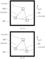
- Fig. 5 is a schematic diagram of light-emitting units in one of light regions shown in Fig. 1 .
- Fig. 5 schematically illustrates one light region including four light-emitting units, in which an M-sided polygon is a quadrilateral.
- the light region 300 may be in the shape of a square, and the M-sided polygon formed by a line of centers of the four light-emitting units 310 located in the light region 300 is a square.
- a vertical component of an emergent optical path of a light-emitting unit e.g., an optical path of h in the direction of the normal n shown in Fig. 3A , may be 100 to 350 ⁇ m.
- h may be 120 to 330 ⁇ m.
- h may be 150 to 300 ⁇ m.
- h may be 170 to 280 ⁇ m.
- h may be 200 to 250 ⁇ m.
- the h is equal to the height difference between the height of the barrier wall and the height of the light-emitting unit, e.g., h is a vertical height difference from a surface of one side of the light-emitting unit away from the substrate to the highest point of the barrier wall.
- the L 1 , L 2 , L 3 , and L 4 refer to horizontal distances from the center of a corresponding light-emitting unit 310 to a vertex angle of the light region, respectively.
- ⁇ 1/2 of the light-emitting unit 310 such as the encapsulated light-emitting diode chip may be 60°, then m ⁇ 1.
- the above relation equation 1 represents a summation relation equation for the corresponding values of N light-emitting units in the light region.
- I 1 /I 2 0.56.
- a ratio of light intensity at the edge position of the light region 300, such as the area E1, to light intensity at the center position of the light region 300, such as an area E2, is not less than 0.5.
- the ratio of the light intensity at the edge position of the light region 300 to the light intensity at the center position of the light region 300 is not less than 0.55.
- the ratio of the light intensity at the edge position of the light region 300 to the light intensity at the center position of the light region 300 is not less than 0.6.
- the ratio of the light intensity at the edge position of the light region 300 to the light intensity at the center position of the light region 300 is not less than 0.65.
- the ratio of the light intensity at the edge position of the light region 300 to the light intensity at the center position of the light region 300 is not less than 0.7.
- the ratio of the light intensity at the edge position of the light region 300 to the light intensity at the center position of the light region 300 is not less than 0.75.
- the ratio of the light intensity at the edge position of the light region 300 to the light intensity at the center position of the light region 300 is not less than 0.8.
- the ratio of the light intensity at the edge position of the light region 300 to the light intensity at the center position of the light region 300 is not less than 0.85.
- the ratio of the light intensity at the edge position of the light region 300 to the light intensity at the center position of the light region 300 is not less than 0.9.
- each light region 300 of at least some of the light regions 300 includes N light-emitting units, where N ⁇ M, a distance from the center of an i-th light-emitting unit 310 to a vertex angle of the light region 300 is L i , i takes a value in a range of 1 to N, and L i , P, and N satisfy: 8.5 ⁇ P ⁇ (1/L 1 +1/L 2 + ...+1/L N ) ⁇ 6.3, where P ⁇ (1/L 1 +1/L 2 +...+1/L N ) can be used as an approximate reference value for the unitless relative light intensity at the edge position.
- the 1/L 1 +1/L 2 +...+1/L N represents the sum of reciprocals of L N of the N light-emitting units.
- the vertex angle of the light region described above may refer to the area E1 shown in Fig. 5 .
- the above relation equation represents a summation relation equation for the corresponding values of N light-emitting units in the light region.
- the ratio of the pitch of the light region 300 to the side length of the quadrilateral is 1.7 to 2.3.
- the ratio of the pitch of the light region 300 to the side length of the quadrilateral is 1.65 to 2.25.
- the ratio of the pitch of the light region 300 to the side length of the quadrilateral is 1.7 to 2.2.
- the ratio of the pitch of the light region 300 to the side length of the quadrilateral is 1.75 to 2.15.
- the ratio of the pitch of the light region 300 to the side length of the quadrilateral is 1.8 to 2.1.
- the ratio of the pitch of the light region 300 to the side length of the quadrilateral is 1.85 to 2.05.
- the ratio of the pitch of the light region 300 to the side length of the quadrilateral is 1.9 to 2.
- each of the at least some of the light regions 300 includes at least four light-emitting units 310, the at least four light-emitting units 310 are arranged to form an M-sided polygon, and an included angle between one of the first direction and the second direction and at least one side of the M-sided polygon is 0 degrees.
- At least some of the light regions 300 are in the shape of a square.
- each light region 300 of the at least some of the light regions 300 is in the shape of a first square
- each light region 300 of the at least some of the light region 300 includes at least four light-emitting units 310
- the centers of the four light-emitting units 310, closest to four vertex angles of the light region 300, among the at least four light-emitting units 310 are sequentially connected to form a second square, and an included angle between a diagonal of the first square and a diagonal of the second square is 0 degrees.
- the diagonal of the first square may coincide with the diagonal of the second square.
- the at least four light-emitting units 310 include four light-emitting units 311, 312, 313, and 314, and the centers of the four light-emitting units 311, 312, 313, and 314 are sequentially connected to form the second square.
- an included angle between each of two sides of the second square and the first direction is 0 degrees
- an included angle between each of two other sides of the second square and the second direction is 0 degrees
- the plurality of light-emitting units 310 in the light region 300 is evenly distributed.
- the pitch of the light region 300 is 4.46 mm
- the pitch of the light-emitting unit 310 is 2.23 mm
- the size of the light-emitting unit 310 may be 0.22 mm ⁇ 0.22 mm.
- the number of light regions 300 may be 2,596, for example, the number of light regions 300 arranged in one of the first direction and the second direction may be 44, and the number of light regions 300 arranged in the other one of the first direction and the second direction may be 59.
- the size of the substrate on which the light regions 300 are disposed may be 263 mm ⁇ 196 mm.
- the total thickness of a light plate formed by the substrate 100, the light-emitting units 310, and the barrier wall pattern 200 may be 0.27 mm.
- tan ⁇ h/L.
- N takes a value of the number of the light-emitting units in the light region, and N may be 4 shown in Fig.
- Ii I 0 ⁇ cosm ⁇ [( ⁇ /2)- (h/L 1i )]+I 0 ⁇ cosm ⁇ [( ⁇ /2)-(h/L 2 )]+I 0 ⁇ cosm ⁇ [( ⁇ /2)-(h/L 3 )]+I 0 ⁇ cos ⁇ [( ⁇ /2)-(h/L 4 )].
- the above relation equation 2 represents a summation relation equation for the corresponding values of the N light-emitting units in the light region.
- the pitch of the light-emitting unit 310 may refer to the side length of the M-sided polygon.
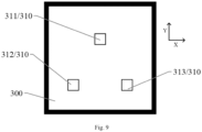
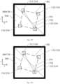
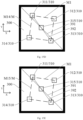
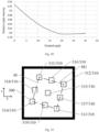
- Figs. 6 to 9 are schematic diagrams of the distribution of light-emitting units in one light region according to various examples of an embodiment of the present disclosure.
- At least one light region 300 in the example shown in Fig. 6 includes five light-emitting units 311, 312, 313, 314, and 315. Centers of the four light-emitting units 311, 312, 313, and 314 are sequentially connected to form a quadrilateral, or the five light-emitting units 311, 312, 313, 314, and 315 are arranged to form a quadrilateral. An included angle between at least one of the first direction and the second direction and at least one side of the quadrilateral is 0 degrees.
- the four light-emitting units 311, 312, 313, and 314 may be the four light-emitting units located outermost, or may be the four light-emitting units closest to vertex angles of the light region.
- the light region 300 includes five light-emitting units.
- a distance from the center of an i-th light-emitting unit 310 to a vertex angle of the light region 300 is L i , i takes a value in the range of 1 to 5, and L i , P, and N satisfy: 8.5 ⁇ P ⁇ 1 /L 1 + 1 /L 2 + 1 /L 3 + 1 /L 4 + 1 /L 5 ⁇ 6.3
- a ratio of the pitch of the light region 300 to a side length of the quadrilateral is 1.7 to 2.3.
- the ratio of the pitch of the light region 300 to the side length of the quadrilateral is 1.65 to 2.25.
- the ratio of the pitch of the light region 300 to the side length of the quadrilateral is 1.7 to 2.2.
- the ratio of the pitch of the light region 300 to the side length of the quadrilateral is 1.75 to 2.15.
- the ratio of the pitch of the light region 300 to the side length of the quadrilateral is 1.8 to 2.1.
- the ratio of the pitch of the light region 300 to the side length of the quadrilateral is 1.85 to 2.05.
- the ratio of the pitch of the light region 300 to the side length of the quadrilateral is 1.9 to 2.
- the five light-emitting units 311, 312, 313, 314, and 315 may be evenly distributed.
- the light-emitting unit 315 may be located at the center of the quadrilateral formed by the four light-emitting units 311, 312, 313, and 314.
- the quadrilateral formed by connecting the centers of the four light-emitting units 311, 312, 313, and 314 sequentially may be a rectangle.
- the quadrilateral formed by connecting the centers of the four light-emitting units 311, 312, 313, and 314 sequentially may be a square.
- an included angle between each of two sides of the quadrilateral and the first direction is 0 degrees
- an included angle between each of the other two sides of the quadrilateral and the second direction is 0 degrees
- the light region 300 is in the shape of the first square
- the quadrilateral formed by connecting the centers of the four light-emitting units 311, 312, 313, and 314 sequentially may be the second square
- an included angle between a diagonal of the first square and a diagonal of the second square is 0 degrees.
- the diagonal of the first square may coincide with the diagonal of the second square.
- the pitch of the light region 300 is 4.46 mm
- the pitch of the light-emitting unit 310 is 2.23 mm
- the size of the light-emitting unit 310 may be 0.22 mm ⁇ 0.22 mm.
- the number of light regions 300 may be 2,596, for example, the number of light regions 300 arranged in one of the first direction and the second direction may be 44, and the number of light regions 300 arranged in the other one of the first direction and the second direction may be 59.
- the size of the substrate on which the light regions 300 are disposed may be 263 mm ⁇ 196 mm.
- parameters such as the size and material of the barrier wall and the size of the light-emitting units in the example shown in Fig. 6 may be the same as the corresponding parameters in the above example and will not be repeated herein.
- the at least one light region 300 in the example shown in Fig. 7 includes nine light-emitting units 311, 312, 313, 314, 315, 316, 317, 318, and 319, centers of the four light-emitting units 311, 312, 313, and 314 are sequentially connected to form a quadrilateral, or the nine light-emitting units 311, 312, 313, 314, 315, 316 317, 318, and 319 are arranged to form a quadrilateral, and an included angle between at least one of the first direction and the second direction and at least one side of the quadrilateral is 0 degrees.
- the four light-emitting units 311, 312, 313, and 314 may be the four light-emitting units located outermost, or may be the four light-emitting units closest to vertex angles of the light region.
- the light region 300 includes nine light-emitting units, and a distance from the center of an i-th light-emitting unit 310 to a vertex angle of the light region 300 is L i , where i takes a value in the range of 1 to 9, and L i , P, and N satisfy: 8.5 ⁇ P ⁇ 1 / L 1 + 1 / L 2 + 1 / L 3 + 1 / L 4 + 1 / L 5 + 1 / L 6 + 1 / L 7 + 1 / L 8 + 1 / L 9 ⁇ 6.3
- the ratio of the pitch of the light region 300 to the side length of the quadrilateral is 1.7 to 2.3.
- the ratio of the pitch of the light region 300 to the side length of the quadrilateral is 1.65 to 2.25.
- the ratio of the pitch of the light region 300 to the side length of the quadrilateral is 1.7 to 2.2.
- the ratio of the pitch of the light region 300 to the side length of the quadrilateral is 1.75 to 2.15.
- the ratio of the pitch of the light region 300 to the side length of the quadrilateral is 1.8 to 2.1.
- the ratio of the pitch of the light region 300 to the side length of the quadrilateral is 1.85 to 2.05.
- the ratio of the pitch of the light region 300 to the side length of the quadrilateral is 1.9 to 2.
- the nine light-emitting units 311, 312, 313, 314, 315, 316, 317, 318, and 319 may be evenly distributed.
- the light-emitting unit 315 may be located at the center of the quadrilateral formed of the four light-emitting units 311, 312, 313, and 314.
- the light-emitting unit 318 may be located between the light-emitting unit 311 and the light-emitting unit 312
- the light-emitting unit 319 may be located between the light-emitting unit 311 and the light-emitting unit 314
- the light-emitting unit 317 may be located between the light-emitting unit 313 and the light-emitting unit 314
- the light-emitting unit 316 may be located between the light-emitting unit 312 and the light-emitting unit 313.
- four sides of the quadrilateral pass through the centers of the light-emitting units 318, 319, 317, and 316, respectively.
- the centers of the light-emitting units 318, 319, 317, and 316 may be the centers of the four sides of the quadrilateral, respectively.
- the quadrilateral formed by connecting the centers of the four light-emitting units 311, 312, 313, and 314 sequentially may be a rectangle.
- the quadrilateral formed by connecting the centers of the four light-emitting units 311, 312, 313, and 314 sequentially may be a square.
- an included angle between two sides of the quadrilateral and the first direction is 0 degrees
- an included angle between the other two sides of the quadrilateral and the second direction is 0 degrees
- the light region 300 is in the shape of the first square
- the quadrilateral formed by connecting the centers of the four light-emitting units 311, 312, 313, and 314 sequentially may be the second square
- an included angle between a diagonal of the first square and a diagonal of the second square is 0 degrees.
- the diagonal of the first square may coincide with the diagonal of the second square.
- the pitch of the light region 300 is 4.46 mm
- the pitch of the light-emitting unit 310 is 2.23 mm
- the size of the light-emitting unit 310 may be 0.22 mm ⁇ 0.22 mm.
- the number of light regions 300 may be 2,596, for example, the number of light regions 300 arranged in one of the first direction and the second direction may be 44, and the number of light regions 300 arranged in the other one of the first direction and the second direction may be 59.
- the size of the substrate on which the light regions 300 are disposed may be 263 mm ⁇ 196 mm.
- parameters such as the size and material of the barrier wall and the size of the light-emitting units in the example shown in Fig. 7 may be the same as the corresponding parameters in the above example and will not be repeated herein.
- the at least one light region 300 in the example shown in Fig. 8 includes seven light-emitting units 311, 312, 313, 314, 315, 316, and 317, centers of the six light-emitting units 311, 312, 313, 314, 316, and 317 are sequentially connected to form hexagon, or the seven light-emitting units 311, 312, 313, 314, 315, 316 and 317 are arranged to form a hexagon, and an included angle between at least one of the first direction and the second direction and at least one side of the hexagon is 0 degrees.
- the six light-emitting units 311, 312, 313, 314, 316, and 317 may be the six light-emitting units located outermost, or may be the six light-emitting units closest to vertex angles of the light region.
- the light region 300 includes seven light-emitting units, and a distance from the center of an i-th light-emitting unit 310 to vertex angles of the light region 300 is L i , where i takes a value in the range of 1 to 7, and L i , P, and N satisfy: 8.5 ⁇ P ⁇ 1 /L 1 + 1 /L 2 + 1 /L 3 + 1 /L 4 + 1 /L 5 + 1 /L 6 + 1 /L 7 ⁇ 6.3
- a ratio of the pitch of the light region 300 to a side length of the hexagon is 1.7 to 2.3.
- the ratio of the pitch of the light region 300 to the side length of the hexagon is 1.65 to 2.25.
- the ratio of the pitch of the light region 300 to the side length of the hexagon is 1.7 to 2.2.
- the ratio of the pitch of the light region 300 to the side length of the hexagon is 1.75 to 2.15.
- the ratio of the pitch of the light region 300 to the side length of the hexagon is 1.8 to 2.1.
- the ratio of the pitch of the light region 300 to the side length of the hexagon is 1.85 to 2.05.
- the ratio of the pitch of the light region 300 to the side length of the hexagon is 1.9 to 2.
- the seven light-emitting units 311, 312, 313, 314, 315, 316, and 317 may be evenly distributed.
- the light-emitting unit 315 may be located in the center of the hexagon formed by the six light-emitting units 311, 312, 313, 314, 316, and 317.
- the hexagon may be a regular hexagon.
- an included angle between each of two sides of the hexagon and the first direction or the second direction is 0 degrees.
- parameters such as the size and material of the barrier wall and the size of the light-emitting units in the example shown in Fig. 8 may be the same as the corresponding parameters in the above example and will not be repeated herein.
- this embodiment of the present disclosure is not limited thereto, and the number of the light-emitting units in the light region may also be six, such as by removing the light-emitting unit 315 located in the very center in Fig. 8 .
- the number of the light-emitting units in the light region may be set according to the needs of the backlight structure and the needs of the display panel.
- At least one light region 300 in the example shown in Fig. 9 includes three light-emitting units 311, 312, and 313, centers of the three light-emitting units 311, 312, and 313 are connected to form a triangle, and an included angle between at least one of the first direction and the second direction and at least one side of the triangle is 0 degrees.
- the three light-emitting units 311, 312, and 313 may be three light-emitting units located outermost.
- the light region 300 includes three light-emitting units, and a distance from the center of an i-th light-emitting unit 310 to a vertex angle of the light region 300 is L i , where i takes a value in the range of 1 to 3, and L i , P, and N satisfy: 8.5 ⁇ P ⁇ (1/L 1 +1/L 2 +1/L 3 ) ⁇ 6.3.
- a ratio of the pitch of the light region 300 to a side length of the triangle is 1.7 to 2.3.
- the ratio of the pitch of the light region 300 to the side length of the triangle is 1.65 to 2.25.
- the ratio of the pitch of the light region 300 to the side length of the triangle is 1.7 to 2.2.
- the ratio of the pitch of the light region 300 to the side length of the triangle is 1.75 to 2.15.
- the ratio of the pitch of the light region 300 to the side length of the triangle is 1.8 to 2.1.
- the ratio of the pitch of the light region 300 to the side length of the triangle is 1.85 to 2.05.
- the ratio of the pitch of the light region 300 to the side length of the triangle is 1.9 to 2.
- the three light-emitting units 311, 312, and 313 may be evenly distributed.
- the triangle may be an equilateral triangle.
- an included angle between one side of the triangle and the first direction or the second direction is 0 degrees.
- the triangle may have an included angle of 0 degrees between one side and the first direction and an included angle of 0 degrees between the other side and the second direction.
- the pitch of the light region 300 is 4.8 mm
- the pitch of the light-emitting unit 310 is 2.6 mm
- the size of the light-emitting unit 310 may be 0.219 mm ⁇ 0.219 mm.
- parameters such as the size and material of the barrier wall and the size of the light-emitting units in the example shown in Fig. 9 may be the same as the corresponding parameters in the above example and will not be repeated herein.
- Fig. 10 is a schematic diagram of a partial planar structure of a backlight structure according to another example of an embodiment of the present disclosure.
- the backlight structure includes a substrate 100, and a barrier wall pattern 200 and a plurality of light-emitting units 310 that are located on the substrate 100.
- the barrier wall pattern 200 includes a plurality of openings 210 arrayed along a first direction and a second direction and a barrier wall 220 surrounding the openings 210, the plurality of openings 210 is configured to define a plurality of light regions 300, and the first direction intersects the second direction.
- the plurality of light-emitting units 310 is distributed in the plurality of light regions 300.
- the substrate 100 includes a central region 101 and an edge region 102 surrounding the central region 101, each light region 300 at least in the central region 101 is provided with at least three light-emitting units 310, centers of M light-emitting units 310, closest to vertex angles of the light region 300, of the at least three light-emitting units 310 are sequentially connected to form an M-sided polygon, a distance between the center of the M-sided polygon and the center of the light region 300 is less than 10% of the pitch of the light region 300, and an included angle between the first direction and each side of the M-sided polygon and an included angle between the second direction and each side of the M-sided polygon are both greater than 0 degrees.
- the setting of the included angle between each side of the M-sided polygon and the first direction and the included angle between each side of the M-sided polygon and the second direction is conducive to improving the light emitting uniformity.
- one of the first direction and the second direction is a direction X shown in Fig. 10
- the other of the first direction and the second direction may be a direction Y shown in Fig. 10 .
- This embodiment of the present disclosure is schematically described with the first direction being the direction X and the second direction being the direction Y.
- the first direction is perpendicular to the second direction.
- an included angle between the first direction and the second direction may be 80 to 110 degrees, or 85 to 100 degrees, or 88 to 92 degrees.
- This embodiment of the present disclosure is not limited thereto, and the first direction may be interchanged with the second direction.
- the included angle between the first direction and each side of the M-sided polygon as well as between the second direction and each side of the M-sided polygon is greater than 0.5 degrees.
- the included angle between the first direction and each side of the M-sided polygon as well as between the second direction and each side of the M-sided polygon is greater than 1 degree.
- the included angle between the first direction and each side of the M-sided polygon as well as between the second direction and each side of the M-sided polygon is greater than 2 degrees.
- the included angle between the first direction and each side of the M-sided polygon as well as between the second direction and each side of the M-sided polygon is greater than 3 degrees.
- the included angle between the first direction and each side of the M-sided polygon as well as between the second direction and each side of the M-sided polygon is greater than 4 degrees.
- the included angle between the first direction and each side of the M-sided polygon as well as between the second direction and each side of the M-sided polygon is greater than 5 degrees.
- the included angle between the first direction and each side of the M-sided polygon as well as between the second direction and each side of the M-sided polygon is greater than 5.5 degrees.
- the included angle between the first direction and each side of the M-sided polygon as well as between the second direction and each side of the M-sided polygon is greater than 6 degrees.
- the included angle between the first direction and each side of the M-sided polygon as well as between the second direction and each side of the M-sided polygon is greater than 6.5 degrees.
- the included angle between the first direction and each side of the M-sided polygon as well as between the second direction and each side of the M-sided polygon is greater than 7 degrees.
- the included angle between the first direction and each side of the M-sided polygon as well as between the second direction and each side of the M-sided polygon is greater than 8 degrees.
- the included angle between the first direction and each side of the M-sided polygon as well as between the second direction and each side of the M-sided polygon is greater than 9 degrees.
- the included angle between the first direction and each side of the M-sided polygon as well as between the second direction and each side of the M-sided polygon is greater than 10 degrees.
- the included angle between the first direction and each side of the M-sided polygon as well as between the second direction and each side of the M-sided polygon is greater than 10.5 degrees.
- the included angle between the first direction and each side of the M-sided polygon as well as between the second direction and each side of the M-sided polygon is greater than 11 degrees.
- the included angle between the first direction and each side of the M-sided polygon as well as between the second direction and each side of the M-sided polygon is greater than 12 degrees.
- the included angle between the first direction and one side of the M-sided polygon may be the same as the included angle between the second direction and another side of the M-sided polygon.
- this embodiment of the present disclosure is not limited thereto, and the included angle between the first direction and one side of the M-sided polygon may be different from the included angle between the second direction and either side of the M-sided polygon.
- the plurality of openings 210 corresponds to the plurality of light regions 300 one by one, and each of the openings 210 is used to define one light region 300.
- the number of the light-emitting units 310 distributed in different light regions 300 may be the same or different.
- the number of light-emitting units 310 distributed in some of the light regions 300 in a region on the substrate 100 is the same, and the number of light-emitting units 310 distributed in some of the light regions 300 in another region on the substrate 100 is different.
- the positions of the two regions described above may be set according to the product requirements, for example, one of the regions may be located in a central region of the substrate, and the other region may be an edge region of the substrate; or one of the regions may be located in the edge region of the substrate, and the other region may be located in the central region of the substrate; or both the two regions are located in different edge regions of the substrate.
- a central region 101 of the substrate 100 may include at least one light region 300.
- the central region 101 may include two light regions 300, four light regions 300, or more light regions 300.
- an edge region 102 includes at least one circle of light regions 300 located at the edge, the at least one circle of light regions 300 includes two columns of light regions 300 located on either side of the central region 101 in a first direction and two rows of light regions 300 located on either side of the central region 101 in a second direction.
- the number of light-emitting units 310 disposed in each of the light regions 300 located in the central region 101 and the edge region 102 respectively are the same.
- the number of light regions included in the central region and the edge region respectively and the number of light-emitting units included in each light region may be set according to product requirements.
- M is not greater than the number of light-emitting units 310 disposed in each light region 300.
- the M-sided polygon may be a triangle, a quadrilateral, a hexagon, or the like. This embodiment of the present disclosure is not limited thereto.
- At least three light-emitting units 310 are disposed in each light region 300 of all the light regions 300.
- each light region 300 may be provided with three light-emitting units 310, or four light-emitting units 310, or five light-emitting units 310, or six light-emitting units 310, or the like.
- the light region 300 may be in the shape of a polygon, such as a triangle, a quadrilateral, a hexagon, or the like.
- the center of the light-emitting unit refers to a geometric center of the light-emitting unit, for example, an orthographic projection of the geometric center on the substrate coincides with the center of a two-dimensional plane of an orthographic projection of the light-emitting unit on the substrate.
- Centers of the M light-emitting units sequentially connected may refer to the centers of the M light-emitting units being connected clockwise or counterclockwise.
- the pitch P of the light region 300 may be the length of a line connecting centers of adjacent light regions 300 arranged in the first direction, or the length of a line connecting centers of adjacent light regions 300 arranged in the second direction.
- a ratio of the pitch of the light region 300 in the first direction to the pitch of the light region 300 in the second direction may be 0.9 to 1.1, e.g., the two pitches may be equal.
- a distance between the center C1 of the M-sided polygon and the center C2 of the light region 300 is less than 9.5% of the pitch P of the light region 300.
- the distance between the center C1 of the M-sided polygon and the center C2 of the light region 300 is less than 9% of the pitch P of the light region 300.
- the distance between the center C1 of the M-sided polygon and the center C2 of the light region 300 is less than 8.5% of the pitch P of the light region 300.
- the distance between the center C1 of the M-sided polygon and the center C2 of the light region 300 is less than 8% of the pitch P of the light region 300.
- the distance between the center C1 of the M-sided polygon and the center C2 of the light region 300 is less than 7.5% of the pitch P of the light region 300.
- the distance between the center C1 of the M-sided polygon and the center C2 of the light region 300 is less than 7% of the pitch P of the light region 300.
- the distance between the center C1 of the M-sided polygon and the center C2 of the light region 300 is less than 6.5% of the pitch P of the light region 300.
- the distance between the center C1 of the M-sided polygon and the center C2 of the light region 300 is less than 6% of the pitch P of the light region 300.
- the distance between the center C1 of the M-sided polygon and the center C2 of the light region 300 is less than 5.5% of the pitch P of the light region 300.
- the distance between the center C1 of the M-sided polygon and the center C2 of the light region 300 is less than 5% of the pitch P of the light region 300.
- the distance between the center C1 of the M-sided polygon and the center C2 of the light region 300 is less than 4.5% of the pitch P of the light region 300.
- the distance between the center C1 of the M-sided polygon and the center C2 of the light region 300 is less than 4% of the pitch P of the light region 300.
- the distance between the center C1 of the M-sided polygon and the center C2 of the light region 300 is less than 3.5% of the pitch P of the light region 300.
- the distance between the center C1 of the M-sided polygon and the center C2 of the light region 300 is less than 3% of the pitch P of the light region 300.
- the distance between the center C1 of the M-sided polygon and the center C2 of the light region 300 is less than 2.5% of the pitch P of the light region 300.
- the distance between the center C1 of the M-sided polygon and the center C2 of the light region 300 is less than 2% of the pitch P of the light region 300.
- the distance between the center C1 of the M-sided polygon and the center C2 of the light region 300 is less than 1.5% of the pitch P of the light region 300.
- the distance between the center C1 of the M-sided polygon and the center C2 of the light region 300 is less than 1% of the pitch P of the light region 300.
- the distance between the center C1 of the M-sided polygon and the center C2 of the light region 300 is less than 0.5% of the pitch P of the light region 300.
- the center C1 of the M-sided polygon coincides with the center C2 of the light region 300.
- a ratio of lengths of different sides of the M-sided polygon is 0.9 to 1.1, and a ratio of the pitch P of the light region 300 to a side length of the M-sided polygon is 1.7 to 2.3.
- the ratio of the lengths of different sides of the M-sided polygon is 0.98 to 1.08.
- the ratio of the lengths of different sides of the M-sided polygon is 0.96 to 1.04.
- the ratio of the lengths of different sides of the M-sided polygon is 0.95 to 1.05.
- the ratio of the lengths of different sides of the M-sided polygon is 0.92 to 1.02.
- all sides of the M-sided polygon are equal in length and are P'.
- the ratio of the pitch P of the light region 300 to the side length P' of the M-sided polygon is 1.65 to 2.25.
- the ratio of the pitch P of the light region 300 to the side length P' of the M-sided polygon is 1.7 to 2.2.
- the ratio of the pitch P of the light region 300 to the side length P' of the M-sided polygon is 1.75 to 2.15.
- the ratio of the pitch P of the light region 300 to the side length P' of the M-sided polygon is 1.8 to 2.1.
- the ratio of the pitch P of the light region 300 to the side length P' of the M-sided polygon is 1.85 to 2.05.
- the ratio of the pitch P of the light region 300 to the side length P' of the M-sided polygon is 1.9 to 2.
- the pitch P of the light region 300 is two times the side length P' of the M-sided polygon.
- the light-emitting units 310 shown in Fig. 10 satisfy the Lambert cosine law of the cosine emitter or the Lambertian emitter shown in Figs. 3A to 3B .
- each of the light-emitting units 310 shown in Fig. 10 includes a light-emitting diode chip 323 and an encapsulation structure 324 configured to encapsulate the light-emitting diode chip 323, as shown in Fig. 2 , and there is a spacing between the encapsulation structures 324 of adjacent light-emitting units 310.
- the light-emitting diode chip 323 may be a sub-millimeter light-emitting diode chip (mini LED), a size of an unencapsulated light-emitting diode chip 323 in a direction perpendicular to the substrate 100 may be 70 ⁇ m to 180 ⁇ m, and the maximum size of the unencapsulated light-emitting diode chip 323 in a direction parallel to the direction of the substrate 100 may be not greater than 500 ⁇ m.
- mini LED sub-millimeter light-emitting diode chip
- the encapsulated light-emitting diode chip is the light-emitting unit 310, and the maximum size in the direction parallel to the substrate 100 and the thickness of the encapsulated light-emitting diode chip 323 are greater than the corresponding parameters of the unencapsulated light-emitting diode chip 323.
- a single light-emitting diode chip 323 may be encapsulated as a stand-alone device to form the light-emitting unit 310 before being disposed at a corresponding position on the backlight structure, and is fixedly connected to a pad on the substrate 100.
- the unencapsulated light-emitting diode chip can be considered as a Lambertian emitter, after the light-emitting diode chip is encapsulated, a light ray emitted at an angle ranging from + ⁇ 1/2 to - ⁇ 1/2 can be emitted, whereas a light ray emitted at an angle in a range other than + ⁇ 1/2 to - ⁇ 1/2 is basically confined to the stand-alone device due to total reflection.
- an included angle ⁇ between an utmost-edge light ray of light rays emitted by the light-emitting unit 310 and the substrate 100 may be a complement angle of ⁇ 1/2 .
- the light-emitting unit 310 or the light-emitting diode chip 323 is connected to a pad 321 on the substrate 100 by a solder metal 322.
- solder metal 322 may include solder tin.
- the encapsulation structure 324 may be doped with a color conversion material 325.
- the color conversion material 325 may include a fluorescent powder material or a quantum dot material.
- the color conversion material 325 may include a material capable of converting blue light to white light.
- the color conversion material 325 may include a material capable of converting blue light to red light and green light.
- the encapsulation structure may not be doped with the color conversion material.
- the light-emitting diode chip 323 may be encapsulated after being disposed at a corresponding position on the substrate 100.
- a transparent material such as transparent silicone
- a transparent material can be used to encapsulate each light-emitting diode chip by means of screen printing or dot printing to form the encapsulation structure 324.
- the light-emitting angle of the light-emitting diode chip 323 can be modulated, thereby changing the light-emitting angle of the light-emitting unit 310.
- a surface of the encapsulation structure 324 away from the substrate 100 may be a curved surface, and the light-emitting angle of the utmost-edge light ray of the light rays emitted by the light-emitting unit 310 is slightly greater than ⁇ 1/2 of the light-emitting diode chip 323. Assuming that the value of ⁇ 1/2 is in the range of 40 to 65 degrees, the value of the light-emitting angle of the utmost-edge light ray of the light rays emitted by the light-emitting unit 310 may be in a range of 50 to 70 degrees.
- the encapsulation structure 324 may have any desired size in the direction perpendicular to the substrate 100.
- the size of the encapsulation structure 324 in the direction perpendicular to the substrate 100 may be less than 0.5 mm.
- the size of the encapsulation structure 324 in the direction perpendicular to the substrate 100 may be between 0.1 and 0.4 mm.
- the size of the encapsulation structure 324 in the direction perpendicular to the substrate 100 may be between 0.2 and 0.4 mm.
- the size of the encapsulation structure 324 in the direction perpendicular to the substrate 100 may be less than 0.3 mm.
- the size of the encapsulation structure 324 in the direction perpendicular to the substrate 100 may be between 0.25 and 0.35 mm.
- the size of the encapsulation structure 324 in the direction perpendicular to the substrate 100 may be between 0.15 and 0.25 mm.
- the size of the encapsulation structure 324 in the direction perpendicular to the substrate 100 may be about 0.2 mm.
- the size of the encapsulation structure 324 in the direction perpendicular to the substrate 100 may be about 0.3 mm.
- the maximum size of the encapsulation structure 324 in the direction parallel to the substrate 100 may be between 0.3 and 2.5 mm.
- the maximum size of the encapsulation structure 324 in the direction parallel to the substrate 100 may be between 0.3 and 2.5 mm.
- the maximum size of the encapsulation structure 324 in the direction parallel to the substrate 100 may be between 0.3 and 0.7 mm.
- the maximum size of the encapsulation structure 324 in the direction parallel to the substrate 100 may be between 0.8 and 0.9 mm.
- the maximum size of the encapsulation structure 324 in the direction parallel to the substrate 100 may be greater than 0.5 mm.
- the maximum size of the encapsulation structure 324 in the direction parallel to the substrate 100 may be greater than 1.0 mm.
- the maximum size of the encapsulation structure 324 in the direction parallel to the substrate 100 may be greater than 2.0 mm.
- the maximum size of the encapsulation structure 324 in the direction parallel to the substrate 100 may be less than 2.0 mm.
- a geometric center of the light-emitting diode chip in an orthographic projection of the light-emitting diode chip on the substrate may coincide with a geometric center of an orthographic projection of the stand-alone device on the substrate.
- the geometric center of the orthographic projection of the light-emitting diode chip on the substrate may also be offset with respect to the geometric center of the orthographic projection of the stand-alone device on the substrate; a height of the light-emitting unit 310 in the direction perpendicular to the substrate 100 is a height of the encapsulated light-emitting diode chip.
- each light-emitting unit 310 in the direction perpendicular to the substrate 100 is not greater than 2 mm.
- a size of the light-emitting unit 310 in a direction perpendicular to the substrate 100 is not greater than 200 ⁇ m.
- the size of the light-emitting unit 310 in the direction perpendicular to the substrate 100 is not greater than 180 ⁇ m.
- the size of the light-emitting unit 310 in the direction perpendicular to the substrate 100 is not greater than 160 ⁇ m.
- the size of the light-emitting unit 310 in the direction perpendicular to the substrate 100 is not greater than 150 ⁇ m.
- the size of the light-emitting unit 310 in the direction perpendicular to the substrate 100 is not greater than 140 ⁇ m.
- the size of the light-emitting unit 310 in the direction perpendicular to the substrate 100 is not greater than 130 ⁇ m.
- the size of the light-emitting unit 310 in the direction perpendicular to the substrate 100 is not greater than 120 ⁇ m.
- the size of the light-emitting unit 310 in the direction perpendicular to the substrate 100 is not greater than 110 ⁇ m.
- the size of the light-emitting unit 310 in the direction perpendicular to the substrate 100 is not greater than 100 ⁇ m.
- the size of the light-emitting unit 310 in the direction perpendicular to the substrate 100 refers to the height of the light-emitting unit 310.
- the height of the light-emitting unit 310 is 50 to 100 ⁇ m.
- the height of the light-emitting unit 310 is 80 to 100 ⁇ m.
- the height of the light-emitting unit 310 is 55 to 95 ⁇ m.
- the height of the light-emitting unit 310 is 60 to 90 ⁇ m.
- the height of the light-emitting unit 310 is 70 to 85 ⁇ m.
- the height of the light-emitting unit 310 is 75 to 80 ⁇ m.
- the light-emitting unit 310 has a maximum size not greater than 3 mm in a direction parallel to the substrate 100.
- the maximum size of the light-emitting unit 310 in the direction parallel to the substrate 100 is not greater than 500 ⁇ m.
- the maximum size of the light-emitting unit 310 in the direction parallel to the substrate 100 is not greater than 450 ⁇ m.
- the maximum size of the light-emitting unit 310 in the direction parallel to the substrate 100 is not greater than 400 ⁇ m.
- the maximum size of the light-emitting unit 310 in the direction parallel to the substrate 100 is not greater than 350 ⁇ m.
- the maximum size of the light-emitting unit 310 in the direction parallel to the substrate 100 is not greater than 330 ⁇ m.
- the maximum size of the light-emitting unit 310 in the direction parallel to the substrate 100 is not greater than 300 ⁇ m.
- the maximum size of the light-emitting unit 310 in the direction parallel to the substrate 100 is not greater than 280 ⁇ m.
- a size of the light-emitting unit 310 in at least one of the first direction and the second direction is not greater than 250 ⁇ m.
- the size of the light-emitting unit 310 in at least one of the first direction and the second direction is not greater than 240 ⁇ m.
- the size of the light-emitting unit 310 in at least one of the first direction and the second direction is not greater than 230 ⁇ m.
- the size of the light-emitting unit 310 in at least one of the first direction and the second direction is not greater than 220 ⁇ m.
- the light-emitting unit 310 has a size of 219 ⁇ m in both the first direction and the second direction.
- the shape of the light-emitting unit described above may refer to the shape of the orthographic projection of the light-emitting unit on the substrate.
- the light-emitting unit may be in the shape of a quadrilateral, such as a rectangle, and the maximum size of the light-emitting unit in the direction parallel to the substrate may be a length of a diagonal of the quadrilateral.
- the light-emitting unit may be in the shape of an oval, and the maximum size of the light-emitting unit in the direction parallel to the substrate may be a length of a long axis of the oval.
- the light-emitting unit may be in the shape of a circle, and the maximum size of the light-emitting unit in the direction parallel to the substrate may be a diameter.
- the light-emitting unit in the example shown in Fig. 10 may further include only the unencapsulated light-emitting diode chip 323, as shown in Fig. 2B .
- the maximum size of the unencapsulated light-emitting diode chip 323 in the direction parallel to the substrate 100 may be not greater than 500 ⁇ m.
- Fig. 11 is a schematic diagram of a partial cross-sectional structure cut along line BB' shown in Fig. 10 according to an example of an embodiment of the present disclosure.
- a thickness of the barrier wall 220 is greater than a height of the light-emitting unit 310 in a direction perpendicular to the substrate 100.
- the thickness of the barrier wall 220 is 200 to 400 ⁇ m and the height of the light-emitting unit 310 is 50 to 100 ⁇ m.
- the thickness of the barrier wall 220 described above refers to the size of the barrier wall 220 in the direction perpendicular to the substrate 100.
- the thickness of the barrier wall 220 is 250 to 270 ⁇ m.
- the thickness of the barrier wall 220 may be 210 to 390 ⁇ m.
- the thickness of the barrier wall 220 may be 220 to 370 ⁇ m.
- the thickness of the barrier wall 220 may be 230 to 350 ⁇ m.
- the thickness of the barrier wall 220 may be 235 to 320 ⁇ m.
- the thickness of the barrier wall 220 may be 240 to 300 ⁇ m.
- the thickness of the barrier wall 220 may be 245 to 280 ⁇ m.
- the barrier wall 220 has a width of 350 to 500 ⁇ m.
- the width of the barrier wall 220 refers to the size, in the first direction, of the barrier wall 220 between two adjacent light regions 300 in the first direction, or the size, in the second direction, of the barrier wall 220 between two adjacent light regions 300 in the second direction.
- the barrier wall 220 has a width of 370 to 480 ⁇ m.
- the width of the barrier wall 220 may be 350 to 450 ⁇ m.
- the width of the barrier wall 220 may be 360 to 440 ⁇ m.
- the width of the barrier wall 220 may be 370 to 430 ⁇ m.
- the width of the barrier wall 220 may be 380 to 420 ⁇ m.
- the width of the barrier wall 220 may be 390 to 410 ⁇ m.
- the width of the barrier wall 220 may be 400 ⁇ m.
- the barrier wall 220 includes a shading material.
- the material of the barrier wall 220 may include black resin.
- the light-emitting units 310 disposed in each light region 300 are electrically connected.
- a plurality of light-emitting units 310 in each light region 300 is connected in series.
- the plurality of light-emitting units 310 in each light region 300 is connected in parallel.
- each light region is surrounded by a circle of barrier wall capable of shading, which is conducive to reducing the crosstalk of light rays between different light regions and alleviate the halo phenomenon.
- At least some of the light regions 300 are in the shape of a rectangle, and two adjacent sides in the rectangle extend in the first direction and the second direction, respectively.
- all of the light regions 300 are in the shape of a rectangle.
- different light regions 300 have the same shape and are of the same size.
- the substrate may be divided into a plurality of regions according to product requirements, the sizes of the light regions in different regions may be different, and the sizes of the light regions in the same region are the same.
- Fig. 12 is a schematic diagram of light-emitting units in one of light regions shown in Fig. 10 .
- One light region including four light-emitting units is schematically illustrated in the example shown in Fig. 12 , in which an M-sided polygon is a quadrilateral.
- the one light region 300 may be in the shape of a square, and the M-sided polygon formed by a line connecting centers of the four light-emitting units 310 located in the light region 300 may be a square.
- each light region 300 of at least some light regions 300 includes N light-emitting units 310, where N ⁇ M, and a distance from the center of an i-th light-emitting unit 310 to a vertex angle of the light region 300 is L i , i takes a value in a range of 1 to N, and L i , P, and N satisfy: 8.5 ⁇ P ⁇ (1/L 1 +1/L 2 +...+1/L N ) ⁇ 6.3, where P ⁇ (1/L 1 +1/L 2 +...+1/L N ) can be used as an approximate reference value for the unitless relative light intensity at the edge position.
- the vertex angle of the light region described above may refer to the area E1 shown in Fig. 12 .
- the light region 300 includes four light-emitting units, and a distance from the center of an i-th light-emitting unit 310 to a vertex angle of the light region 300 is L i , where i takes a value in the range of 1 to 4, and L i , P, and N satisfy: 8 .5 ⁇ P ⁇ 1/L 1 + 1/L 2 + 1/L 3 + 1/L 4 ⁇ 6 .3
- the value of L 1 is 1.123379 ⁇ m
- the value of L 2 is 3.363531 ⁇ m
- the value of L 3 is 4.149638 ⁇ m
- the value of L 4 is 2.669986 ⁇ m.
- the four light-emitting units 310 included in the light region 300 form a quadrilateral, and an included angle between one of the first direction and the second direction and at least one side of the quadrilateral is 12 degrees.
- the light region 300 is in the shape of a first square, centers of the four light-emitting units 310 included in the light region 300 are sequentially connected to form a second square, and an included angle between a diagonal of the first square and a diagonal of the second square is 12 degrees.
- the light intensity in the edge region of the light region is increased by rotating the M-sided polygon formed by the light-emitting units in the light region so that neither side of the M-sided polygon is parallel to the first direction and the second direction.
- a ratio of light intensity at the edge position of the light region 300, such as an area E1, to light intensity at the center position of the light region 300 is not less than 0.5.
- the ratio of the light intensity at the edge position of the light region 300 to the light intensity at the center position of the light region 300 is not less than 0.55.
- the ratio of the light intensity at the edge position of the light region 300 to the light intensity at the center position of the light region 300 is not less than 0.6.
- the ratio of the light intensity at the edge position of the light region 300 to the light intensity at the center position of the light region 300 is not less than 0.65.
- the ratio of the light intensity at the edge position of the light region 300 to the light intensity at the center position of the light region 300 is not less than 0.7.
- the ratio of the light intensity at the edge position of the light region 300 to the light intensity at the center position of the light region 300 is not less than 0.75.
- the ratio of the light intensity at the edge position of the light region 300 to the light intensity at the center position of the light region 300 is not less than 0.8.
- the ratio of the light intensity at the edge position of the light region 300 to the light intensity at the center position of the light region 300 is not less than 0.85.
- the ratio of the light intensity at the edge position of the light region 300 to the light intensity at the center position of the light region 300 is not less than 0.9.
- a ratio of the pitch of the light region 300 to a side length of the quadrilateral is 1.7 to 2.3.
- the ratio of the pitch of the light region 300 to the side length of the quadrilateral is 1.65 to 2.25.
- the ratio of the pitch of the light region 300 to the side length of the quadrilateral is 1.7 to 2.2.
- the ratio of the pitch of the light region 300 to the side length of the quadrilateral is 1.75 to 2.15.
- the ratio of the pitch of the light region 300 to the side length of the quadrilateral is 1.8 to 2.1.
- the ratio of the pitch of the light region 300 to the side length of the quadrilateral is 1.85 to 2.05.
- the ratio of the pitch of the light region 300 to the side length of the quadrilateral is 1.9 to 2.
- At least some of the light regions 300 are in the shape of a rectangle, and two adjacent sides in the rectangle extend in the first direction and the second direction, respectively.
- all of the light regions 300 are in the shape of a rectangle.
- the light regions 300 are in the shape of a square.
- tan ⁇ h/L.
- I 1 I 0 ⁇ cosm ⁇ [( ⁇ /2)-(h/L 1 )]+I 0 ⁇ cosm ⁇ [( ⁇ /2)-(h/L 2 )]+...+I 0 ⁇ cosm ⁇ [( ⁇ /2)-(h/L N )], where N takes the value of the number of light-emitting units in the light region, and N may be 4 shown in Fig.
- I 1 I 0 ⁇ cosm ⁇ [( ⁇ /2)- (h/L 1 )]+I 0 ⁇ cosm ⁇ [( ⁇ / 2 )-(h/L2)]+I 0 ⁇ cosm ⁇ [(n/ 2 )-(h/L3)]+ I 0 ⁇ cosm ⁇ [( ⁇ /2)-(h/L N )].
- the included angle between each of the sides of the M-sided polygon shown in Fig. 12 and the first direction or the second direction is not changed, for example, the included angle is 12 degrees, and only the pitch of the light region 300 shown in Fig. 12 and the side length of the M-sided polygon formed by the light-emitting units 310 are adjusted, for example, the pitch of the light region 300 is adjusted to be 5.12 mm, the side length of the M-sided polygon is 2.56 ⁇ m, and then the value of L 1 is 1.162167 ⁇ m, the value of L 2 is 4.156017 ⁇ m, the value of L 3 is 5.113352 ⁇ m, and the value of L 4 is 3.43394 ⁇ m.
- the backlight structure provided in the embodiment of the present disclosure, by rotating the M-sided polygon formed by the light-emitting units in the light region and adjusting the pitch of the light region and the side length of the M-sided polygon, it is beneficial to further improve the light intensity in the edge region of the light region.
- Figs. 13A to 13G are schematic diagrams of one light region according to another example of an embodiment of the present disclosure.
- Fig. 14 is a relationship diagram of relative light intensity at the edge position of the light region after an M-sided polygon in the light region shown in Figs. 13A to 13G respectively is rotated at different angles.
- the rotation of the M-sided polygon at different angles may refer to rotating the M-sided polygon at a certain angle in a certain region where the center of the M-sided polygon is located, for example, a square is rotated at a certain angle in a certain region where the center of the square is located.
- the rotation mentioned above may refer to rotating the M-sided polygon clockwise or rotating the M-sided polygon counterclockwise.
- a difference between the light region shown in Figs. 13A to 13G and the light region shown in Fig. 12 is that the included angle between each side of the M-sided polygon and either of the first direction and the second direction is different.
- an included angle between a diagonal 392 of the second square M01 and a diagonal 391 of the first square shown in Fig. 13A may be 5 degrees; an included angle between a diagonal 392 of the second square M02 and the diagonal 391 of the first square shown in Fig. 13B may be 10 degrees; an included angle between a diagonal 392 of the second square M03 and the diagonal 391 of the first square shown in Fig. 13C may be 13 degrees; an included angle between a diagonal 392 of the second square M04 and the diagonal 391 of the first square shown in Fig. 13D may be 15 degrees; an included angle between a diagonal 392 of the second square M05 and the diagonal 391 of the first square shown in Fig.
- this embodiment of the present disclosure is not limited to rotating the M-shaped polygon at the degrees described above, and degrees of rotation of the M-sided polygon may be selected according to the product requirements.
- each light region 300 of the at least some of the light regions 300 includes at least four light-emitting units 310, the at least four light-emitting units 310 are arranged to form an M-sided polygon, and an included angle between one of the first direction and the second direction and at least one side of the M-sided polygon is 12 to 18 degrees.
- each light region 300 of the at least some of the light regions 300 is in the shape of the first square
- each light region 300 of the at least some of the light region 300 includes at least four light-emitting units 310, and the centers of the four light-emitting units 310, closest to four vertex angles of the light region 300, among the at least four light-emitting units 310 are sequentially connected to form the second square, and an included angle between a diagonal of the first square and a diagonal of the second square is 12 to 18 degrees.
- each light region 300 of the at least some of the light regions 300 includes four light-emitting units 311, 312, 313, and 314, the four light-emitting units 311, 312, 313, and 314 are arranged to form a quadrilateral, and an included angle between one of the first direction and the second direction and at least one side of the quadrilateral is 12 to 18 degrees.
- the light region 300 is in the shape of a first square
- centers of the four light-emitting units 310 included in the light region 300 are sequentially connected to form a second square
- an included angle between a diagonal of the first square and a diagonal of the second square may be 5 degrees, 10 degrees, 13 degrees, 15 degrees, 17 degrees, 20 degrees, or 30 degrees.
- this embodiment of the present disclosure is not limited to the included angle between the diagonal of the first square and the diagonal of the second square being the above-mentioned degrees, and the included angle between the diagonal of the first square and the diagonal of the second square may be selected according to the product requirements.
- a ratio of the pitch of the light region 300 to a side length of the second square is 1.7 to 2.3.
- the ratio of the pitch of the light region 300 to the side length of the second square is 1.65 to 2.25.
- the ratio of the pitch of the light region 300 to the side length of the second square is 1.7 to 2.2.
- the ratio of the pitch of the light region 300 to the side length of the second square is 1.75 to 2.15.
- the ratio of the pitch of the light region 300 to the side length of the second square is 1.8 to 2.1.
- the ratio of the pitch of the light region 300 to the side length of the second square is 1.85 to 2.05.
- the ratio of the pitch of the light region 300 to the side length of the second square is 1.9 to 2.
- the size of the light-emitting unit 310 may be 0.219 mm ⁇ 0.219 mm.
- the value of the relative light intensity Q at the edge position of the light region is larger.
- the angle of the M-sided polygon formed by the arrangement of light-emitting units in the light region to a certain range, e.g., 12 to 18 degrees, and by setting the pitch of the light region and the side length of the M-sided polygon, improvement of the light intensity at the edge of the light region is facilitated, thereby improving the light emitting uniformity of the light region.
- the included angle between the diagonal of the first square and the diagonal of the second square is 13 to 17 degrees.
- the included angle between the diagonal of the first square and the diagonal of the second square is 14.5 to 16.5 degrees.
- the included angle between the diagonal of the first square and the diagonal of the second square is 15 to 16 degrees.
- the ratio of the light intensity at the edge position of the light region 300, such as a vertex angle area, to the light intensity at the center position of the light region 300 is not less than 0.5.
- the ratio of the light intensity at the edge position of the light region 300 to the light intensity at the center position of the light region 300 is not less than 0.55.
- the ratio of the light intensity at the edge position of the light region 300 to the light intensity at the center position of the light region 300 is not less than 0.6.
- the ratio of the light intensity at the edge position of the light region 300 to the light intensity at the center position of the light region 300 is not less than 0.65.
- the ratio of the light intensity at the edge position of the light region 300 to the light intensity at the center position of the light region 300 is not less than 0.7.
- the ratio of the light intensity at the edge position of the light region 300 to the light intensity at the center position of the light region 300 is not less than 0.75.
- the ratio of the light intensity at the edge position of the light region 300 to the light intensity at the center position of the light region 300 is not less than 0.8.
- the ratio of the light intensity at the edge position of the light region 300 to the light intensity at the center position of the light region 300 is not less than 0.85.
- the ratio of the light intensity at the edge position of the light region 300 to the light intensity at the center position of the light region 300 is not less than 0.9.
- Figs. 15A to 15G are schematic diagrams of one light region according to another example of an embodiment of the present disclosure.
- Fig. 16 is a relationship diagram of relative light intensity at the edge position of the light region after an M-sided polygon in the light region shown in Figs. 15A to 15G respectively is rotated at different angles.
- an included angle between a side M1 of an M-sided polygon M11 and a first direction shown in Fig. 15A may be 5 degrees
- an included angle between a side M1 of an M-sided polygon M12 and the first direction shown in Fig. 15B may be 10 degrees
- an included angle between a side M1 of an M-sided polygon M13 and the first direction shown in Fig. 15C may be 13 degrees
- an included angle between a side M1 of an M-sided polygon M14 and the first direction shown in Fig. 15D may be 15 degrees
- an included angle between a side M1 of an M-sided polygon M16 and the first direction shown in Fig. 15F may be 20 degrees
- an included angle between a side M1 of an M-sided polygon M17 and the first direction shown in Fig. 15G may be 30 degrees.
- an included angle between a diagonal 392 of the second square M1 1 and a diagonal 391 of the first square shown in Fig. 15A may be 5 degrees
- an included angle between a diagonal 392 of the second square M12 and the diagonal 391 of the first square shown in Fig. 15B may be 10 degrees
- an included angle between a diagonal 392 of the second square M13 and the diagonal 391 of the first square shown in Fig. 15C may be 13 degrees
- an included angle between a diagonal 392 of the second square M14 and the diagonal 391 of the first square shown in Fig. 15D may be 15 degrees
- 15E may be 17 degrees
- an included angle between a diagonal 392 of the second square M16 and the diagonal 391 of the first square shown in Fig. 15F may be 20 degrees
- an included angle between a diagonal 392 of the second square M17 and the diagonal 391 of the first square may be 30 degrees.
- the rotation of the M-sided polygon at different angles may refer to rotating the M-sided polygon at a certain angle in a certain area where the center of the M-sided polygon is located, for example, a square is rotated at a certain angle in a certain area where the center of the square is located.
- the rotation mentioned above may refer to rotating the M-sided polygon clockwise or rotating the M-sided polygon counterclockwise.
- each of the at least some of the light regions 300 includes at least four light-emitting units 310, the at least four light-emitting units 310 are arranged to form an M-sided polygon, and an included angle between one of the first direction and the second direction and at least one side of the M-sided polygon is 12 to 18 degrees.
- each light region 300 of the at least some of the light regions 300 is in the shape of a first square
- each light region 300 of the at least some of the light region 300 includes at least four light-emitting units 310, and centers of the four light-emitting units 310, closest to four vertex angles of the light region 300, among the at least four light-emitting units 310 are sequentially connected to form a second square, and an included angle between a diagonal of the first square and a diagonal of the second square is 12 to 18 degrees.
- the quadrilateral formed by arranging the four light-emitting units 310 as shown in Figs. 13A to 13G and the quadrilateral formed by arranging the five light-emitting units 310 as shown in Figs. 15A to 15G may have the same shape and size, but without limitation, at least one of the two parameters, i.e., the shape and size, of the two may be different.
- the at least four light-emitting units 310 include five light-emitting units 310, and centers of four light-emitting units 310, located at the utmost edge, among the five light-emitting units 310 are sequentially connected to form the second square.
- each light region 300 of the at least some of the light regions 300 includes five light-emitting units 311, 312, 313, 314 and 315, the five light-emitting units 311, 312, 313, 314 and 315 are arranged to form a quadrilateral, and an included angle between one of the first direction and the second direction and at least one side of the quadrilateral is 12 to 18 degrees.
- the four light-emitting units 311, 312, 313, and 314 are arranged to form a quadrilateral, and the light-emitting unit 315 is located in the center of the four light-emitting units 311, 312, 313, and 314.
- the light region 300 is in the shape of the first square
- centers of the four light-emitting units 310 among the five light-emitting units 310 that are located at the utmost edge and included in the light region 300 are sequentially connected to form the second square
- an included angle between a diagonal of the first square and a diagonal of the second square may be 5 degrees, 10 degrees, 13 degrees, 15 degrees, 17 degrees, 20 degrees, or 30 degrees.
- this embodiment of the present disclosure is not limited to the included angle between the diagonal of the first square and the diagonal of the second square being the above-mentioned degrees, and the included angle between the diagonal of the first square and the diagonal of the second square may be selected according to the product requirements.
- a ratio of the pitch of the light region 300 to a side length of the second square is 1.7 to 2.3.
- the ratio of the pitch of the light region 300 to the side length of the second square is 1.65 to 2.25.
- the ratio of the pitch of the light region 300 to the side length of the second square is 1.7 to 2.2.
- the ratio of the pitch of the light region 300 to the side length of the second square is 1.75 to 2.15.
- the ratio of the pitch of the light region 300 to the side length of the second square is 1.8 to 2.1.
- the ratio of the pitch of the light region 300 to the side length of the second square is 1.85 to 2.05.
- the ratio of the pitch of the light region 300 to the side length of the second square is 1.9 to 2.
- Q P ⁇ (1/L 1 +1/L 2 +1/L 3 +1/L 4 +1/L 5 ), 8.5 ⁇ Q ⁇ 6.3.
- the size of the light-emitting unit 310 may be 0.219 mm ⁇ 0.219 mm.
- the value of the relative light intensity Q at the edge position of the light region is larger.
- the angle of the M-sided polygon formed by the arrangement of light-emitting units in the light region to a certain range, e.g., 12 to 18 degrees, and by setting the number of the light-emitting units in the light region, the pitch of the light region and the side length of the M-sided polygon, improvement of the light intensity at the edge of the light region is facilitated, thereby improving the light emitting uniformity of the light region.
- the light intensity at the edge position of the light region 300 is greater than the light intensity at the edge position of the light region 300 when the number of light-emitting units 310 in the light region 300 is four.
- the included angle between the diagonal of the first square and the diagonal of the second square is 13 to 17 degrees.
- the included angle between the diagonal of the first square and the diagonal of the second square is 14.5 to 16.5 degrees.
- the included angle between the diagonal of the first square and the diagonal of the second square is 15 to 16 degrees.
- the ratio of the light intensity at the edge position of the light region 300, such as a vertex angle area, to the light intensity at the center position of the light region 300 is not less than 0.5.
- the ratio of the light intensity at the edge position of the light region 300 to the light intensity at the center position of the light region 300 is not less than 0.55.
- the ratio of the light intensity at the edge position of the light region 300 to the light intensity at the center position of the light region 300 is not less than 0.6.
- the ratio of the light intensity at the edge position of the light region 300 to the light intensity at the center position of the light region 300 is not less than 0.65.
- the ratio of the light intensity at the edge position of the light region 300 to the light intensity at the center position of the light region 300 is not less than 0.7.
- the ratio of the light intensity at the edge position of the light region 300 to the light intensity at the center position of the light region 300 is not less than 0.75.
- the ratio of the light intensity at the edge position of the light region 300 to the light intensity at the center position of the light region 300 is not less than 0.8.
- the ratio of the light intensity at the edge position of the light region 300 to the light intensity at the center position of the light region 300 is not less than 0.85.
- the ratio of the light intensity at the edge position of the light region 300 to the light intensity at the center position of the light region 300 is not less than 0.9.
- the size, material and other parameters of the barrier wall in the example shown in Figs. 15A to 15G may be the same as the corresponding parameters in the above example and will not be repeated herein.
- Figs. 17A to 17G are schematic diagrams of one light region according to another example of an embodiment of the present disclosure.
- Fig. 18 is a relationship diagram of relative light intensity at the edge position of a light region after an M-sided polygon in the light region shown in Figs. 17A to 17G respectively is rotated at different angles.
- an included angle between a side M2 of a triangle M21 and a first direction shown in Fig. 17A may be 5 degrees
- an included angle between a side M2 of a triangle M22 and the first direction shown in Fig. 17B may be 10 degrees
- an included angle between a side M2 of a triangle M23 and the first direction shown in Fig. 17C may be 13 degrees
- an included angle between a side M2 of a triangle M24 and the first direction shown in Fig. 17D may be 15 degrees
- an included angle between a side M2 of a triangle M25 and the first direction shown in Fig. 17E may be 17 degrees
- 17F may be 20 degrees, and an included angle between a side M2 of a triangle M27 and the first direction shown in Fig. 17G may be 30 degrees.
- this embodiment of the present disclosure is not limited to the included angle between one side of the triangle and the first direction being the above mentioned degrees, and the included angle between the side of the triangle and the first direction may be selected according to the product requirements.
- the rotation of the M-sided polygon at different angles may refer to rotating the M-sided polygon at a certain angle in a certain area where the center of the triangle is located, for example, a triangle is rotated by a certain angle in a certain area where the center of the triangle is located.
- the rotation mentioned above may refer to rotating the M-sided polygon clockwise or rotating the M-sided polygon counterclockwise.
- a difference between the light region shown in Figs. 17A to Fig. 17G and the light region shown in Figs. 13A to Fig. 13G and Figs. 15A to Fig. 15G is that the M-sided polygons are different in shape, e.g., the M-sided polygon shown in Figs. 17A to Fig. 17G may be a triangle.
- each light region 300 of at least some of the light regions 300 includes three light-emitting units 311, 312, and 313, centers of the three light-emitting units 311, 312, and 313 are sequentially connected to form a triangle, and an included angle between one of the first direction and the second direction and one side M2 of the triangle is less than 5 degrees.
- a ratio of the pitch of the light region 300 to a side length of the triangle is 1.7 to 2.3.
- the ratio of the pitch of the light region 300 to the side length of the triangle is 1.65 to 2.25.
- the ratio of the pitch of the light region 300 to the side length of the triangle is 1.7 to 2.2.
- the ratio of the pitch of the light region 300 to the side length of the triangle is 1.75 to 2.15.
- the ratio of the pitch of the light region 300 to the side length of the triangle is 1.8 to 2.1.
- the ratio of the pitch of the light region 300 to the side length of the triangle is 1.85 to 2.05.
- the ratio of the pitch of the light region 300 to the side length of the triangle is 1.9 to 2.
- the size of the light-emitting unit 310 may be 0.219 mm ⁇ 0.219 mm.
- the included angle between one of the first direction and the second direction and one side M2 of the triangle is set to be small, which is conducive to increasing the light intensity at the edge position of the light region, thereby improving the light emitting uniformity of the light region.
- the included angle between the first direction or the second direction and the side M2 of the triangle is less than 4.5 degrees.
- the included angle between the first direction or the second direction and the side M2 of the triangle is less than 4 degrees.
- the included angle between the first direction or the second direction and the side M2 of the triangle is less than 3.5 degrees.
- the included angle between the first direction or the second direction and the side M2 of the triangle is less than 3 degrees.
- the included angle between the first direction or the second direction and the side M2 of the triangle is less than 2.5 degrees.
- the included angle between the first direction or the second direction and the side M2 of the triangle is less than 2 degrees.
- the included angle between the first direction or the second direction and the side M2 of the triangle is less than 1.5 degrees.
- the included angle between the first direction or the second direction and the side M2 of the triangle is less than 1 degree.
- the included angle between the first direction or the second direction and the side M2 of the triangle is less than 0.5 degrees.
- the ratio of the light intensity at the edge position of the light region 300, such as a vertex angle area, to the light intensity at the center position of the light region 300 is not less than 0.5.
- the ratio of the light intensity at the edge position of the light region 300 to the light intensity at the center position of the light region 300 is not less than 0.55.
- the ratio of the light intensity at the edge position of the light region 300 to the light intensity at the center position of the light region 300 is not less than 0.6.
- the ratio of the light intensity at the edge position of the light region 300 to the light intensity at the center position of the light region 300 is not less than 0.65.
- the ratio of the light intensity at the edge position of the light region 300 to the light intensity at the center position of the light region 300 is not less than 0.7.
- the ratio of the light intensity at the edge position of the light region 300 to the light intensity at the center position of the light region 300 is not less than 0.75.
- the ratio of the light intensity at the edge position of the light region 300 to the light intensity at the center position of the light region 300 is not less than 0.8.
- the ratio of the light intensity at the edge position of the light region 300 to the light intensity at the center position of the light region 300 is not less than 0.85.
- the ratio of the light intensity at the edge position of the light region 300 to the light intensity at the center position of the light region 300 is not less than 0.9.
- the size, material and other parameters of the barrier wall in the example shown in Figs. 17A to 17G may be the same as the corresponding parameters in the above example and will not be repeated herein.
- Fig. 19 is a schematic diagram of the distribution of light-emitting units in one light region in different examples of an embodiment of the present disclosure.
- the at least one light region 300 in the example shown in Fig. 19 includes nine light-emitting units 311, 312, 313, 314, 315, 316, 317, 318, and 319, centers of the four light-emitting units 311, 312, 313, and 314 among them are sequentially connected to form a quadrilateral, or the nine light-emitting units 311, 312, 313, 314, 315, 316, 317, 318, and 319 are arranged to form a quadrilateral, and an included angle between at least one of the first direction and the second direction and at least one side of the quadrilateral is 0 degrees.
- the four light-emitting units 311, 312, 313, and 314 may be the four light-emitting units located outermost, or may be the four light-emitting units closest to vertex angles of the light region.
- the included angle between the first direction and each side of the M-sided polygon as well as between the second direction and each side of the M-sided polygon is greater than 0.5 degrees.
- the included angle between the first direction and each side of the M-sided polygon as well as between the second direction and each side of the M-sided polygon is greater than 1 degree.
- the included angle between the first direction and each side of the M-sided polygon as well as between the second direction and each side of the M-sided polygon is greater than 2 degrees.
- the included angle between the first direction and each side of the M-sided polygon as well as between the second direction and each side of the M-sided polygon is greater than 3 degrees.
- the included angle between the first direction and each side of the M-sided polygon as well as between the second direction and each side of the M-sided polygon is greater than 4 degrees.
- the included angle between the first direction and each side of the M-sided polygon as well as between the second direction and each side of the M-sided polygon is greater than 5 degrees.
- the included angle between the first direction and each side of the M-sided polygon as well as between the second direction and each side of the M-sided polygon is greater than 5.5 degrees.
- the included angle between the first direction and each side of the M-sided polygon as well as between the second direction and each side of the M-sided polygon is greater than 6 degrees.
- the included angle between the first direction and each side of the M-sided polygon as well as between the second direction and each side of the M-sided polygon is greater than 6.5 degrees.
- the included angle between the first direction and each side of the M-sided polygon as well as between the second direction and each side of the M-sided polygon is greater than 7 degrees.
- the included angle between the first direction and each side of the M-sided polygon as well as between the second direction and each side of the M-sided polygon is greater than 8 degrees.
- the included angle between the first direction and each side of the M-sided polygon as well as between the second direction and each side of the M-sided polygon is greater than 9 degrees.
- the included angle between the first direction and each side of the M-sided polygon as well as between the second direction and each side of the M-sided polygon is greater than 10 degrees.
- the included angle between the first direction and each side of the M-sided polygon as well as between the second direction and each side of the M-sided polygon is greater than 10.5 degrees.
- the included angle between the first direction and each side of the M-sided polygon as well as between the second direction and each side of the M-sided polygon is greater than 11 degrees.
- the included angle between the first direction and each side of the M-sided polygon as well as between the second direction and each side of the M-sided polygon is greater than 12 degrees.
- the included angle between a side M1 of the M-sided polygon and the first direction is 12 to 18 degrees.
- the included angle between the side M1 of the M-sided polygon and the first direction is 12.5 to 17.5 degrees.
- the included angle between the side M1 of the M-sided polygon and the first direction is 13 to 17 degrees.
- the included angle between the side M1 of the M-sided polygon and the first direction is 13.5 to 16.5 degrees.
- the included angle between the side M1 of the M-sided polygon and the first direction is 14 to 16 degrees.
- the included angle between the side M1 of the M-sided polygon and the first direction is 14.5 to 15 degrees.
- the light region 300 includes nine light-emitting units, and a distance from the center of an i-th light-emitting unit 310 to a vertex angle of the light region 300 is L i , where i takes a value in the range of 1 to 9, and L i , P, and N satisfy: 8.5 ⁇ P ⁇ (1/L 1 +1/L 2 +1/L 3 +1/L 4 +1/L 5 +1/L 6 +1/L 7 +1/L 8 +1/L 9 ) ⁇ 6.3.
- a ratio of the pitch of the light region 300 to a side length of the quadrilateral is 1.7 to 2.3.
- the ratio of the pitch of the light region 300 to the side length of the quadrilateral is 1.65 to 2.25.
- the ratio of the pitch of the light region 300 to the side length of the quadrilateral is 1.7 to 2.2.
- the ratio of the pitch of the light region 300 to the side length of the quadrilateral is 1.75 to 2.15.
- the ratio of the pitch of the light region 300 to the side length of the quadrilateral is 1.8 to 2.1.
- the ratio of the pitch of the light region 300 to the side length of the quadrilateral is 1.85 to 2.05.
- the ratio of the pitch of the light region 300 to the side length of the quadrilateral is 1.9 to 2.
- the nine light-emitting units 311, 312, 313, 314, 315, 316, 317, 318, and 319 may be evenly distributed.
- the light-emitting unit 315 may be located in the center of the quadrilateral formed of the four light-emitting units 311, 312, 313, and 314.
- the light-emitting unit 318 may be located between the light-emitting unit 311 and the light-emitting unit 314, the light-emitting unit 319 may be located between the light-emitting unit 313 and the light-emitting unit 314, the light-emitting unit 317 may be located between the light-emitting unit 313 and the light-emitting unit 312, and the light-emitting unit 316 may be located between the light-emitting unit 312 and the light-emitting unit 311.
- four sides of the quadrilateral pass through the centers of the light-emitting units 318, 319, 317, and 316, respectively.
- the centers of the light-emitting units 318, 319, 317, and 316 may be the centers of the four sides of the quadrilateral, respectively.
- the quadrilateral formed by connecting the centers of the four light-emitting units 311, 312, 313, and 314 sequentially may be a rectangle.
- the quadrilateral formed by connecting the centers of the four light-emitting units 311, 312, 313, and 314 sequentially may be a square.
- an included angle between each of two sides of the quadrilateral and the first direction is greater than 0 degrees
- an included angle between each of the other two sides of the quadrilateral and the second direction is greater than 0 degrees.
- the light region 300 is in the shape of the first square
- the quadrilateral formed by connecting the centers of the four light-emitting units 311, 312, 313, and 314 sequentially may be the second square
- the included angle between a diagonal of the first square and a diagonal of the second square is greater than 0 degrees.
- the ratio of the light intensity at the edge position of the light region 300, such as a vertex angle area, to the light intensity at the center position of the light region 300 is not less than 0.5.
- the ratio of the light intensity at the edge position of the light region 300 to the light intensity at the center position of the light region 300 is not less than 0.55.
- the ratio of the light intensity at the edge position of the light region 300 to the light intensity at the center position of the light region 300 is not less than 0.6.
- the ratio of the light intensity at the edge position of the light region 300 to the light intensity at the center position of the light region 300 is not less than 0.65.
- the ratio of the light intensity at the edge position of the light region 300 to the light intensity at the center position of the light region 300 is not less than 0.7.
- the ratio of the light intensity at the edge position of the light region 300 to the light intensity at the center position of the light region 300 is not less than 0.75.
- the ratio of the light intensity at the edge position of the light region 300 to the light intensity at the center position of the light region 300 is not less than 0.8.
- the ratio of the light intensity at the edge position of the light region 300 to the light intensity at the center position of the light region 300 is not less than 0.85.
- the ratio of the light intensity at the edge position of the light region 300 to the light intensity at the center position of the light region 300 is not less than 0.9.
- parameters such as the size and material of the barrier wall and the size of the light-emitting units in the example shown in Fig. 19 may be the same as the corresponding parameters in the above example and will not be repeated herein.
- This embodiment of the present disclosure is not limited to the shape of the light region being the rectangle as shown in Figs. 1 to 19 .
- the shape of the light region may be designed according to the needs of a display panel corresponding to the backlight structure.
- the light region may be in the shape of a hexagon or octagon or the like.
- This embodiment of the present disclosure is not limited to the number of light-emitting units in the light region being three, four, five, seven, or nine as shown in Figs. 1 to 19 .
- the number can be set according to the position and size of the light-emitting units, for example, the number of light-emitting units in the light region may be six, eight, ten, eleven, twelve, etc.
- the number of light-emitting units in the light region, the side length of the M-sided polygon, the pitch of the light region, and the included angle between the side of the M-sided polygon and the first direction or the second direction are set in a coordinated manner, which is conducive to increasing the light intensity at the edge position of the light region, thereby improving the light emitting uniformity of the light region.
- Fig. 20 is a schematic diagram of a partial cross-section cut along line AA' shown in Fig. 1 according to another example of an embodiment of the present disclosure.
- Fig. 21 is a schematic diagram of a partial cross-section cut along line BB' shown in Fig. 10 according to another example of an embodiment of the present disclosure.
- the backlight structure further includes a flat adhesive 400 located between a barrier wall 220 and each light-emitting unit 310, and between two adjacent light-emitting units 310.
- a thickness of the flat adhesive 400 is not less than a height of the light-emitting unit 310 and is less than a thickness of the barrier wall 220.
- An orthographic projection, on the substrate 100, of a surface of one side of the flat adhesive 400 close to the substrate 100 is completely located in an orthographic projection, on the substrate 100, of a surface of one side of the flat adhesive 400 away from the substrate 100.
- the flat adhesive 400 may fill at least a portion of a gap between the barrier wall 220 and the light-emitting unit 310, and at least a portion of a gap between adjacent light-emitting units 310.
- the thickness of the flat adhesive 400 may be greater than or equal to the height of the light-emitting unit 310.
- the flat adhesive 400 may be made of white oil.
- the thickness of the flat adhesive 400 may be 50 ⁇ m.
- the thickness of the flat adhesive 400 may be greater than 90 ⁇ m.
- the thickness of the flat glue 400 may be less than 250 ⁇ m.
- the thickness of the flat glue 400 may be less than 200 ⁇ m.
- the thickness of the flat glue 400 may be less than 180 ⁇ m.
- the thickness of the flat glue 400 may be less than 150 ⁇ m.
- the thickness of the flat glue 400 may be less than 120 ⁇ m.
- the thickness of the flat glue 400 may be less than 100 ⁇ m.
- the cross section of the flat adhesive 400 intercepted by a plane (e.g. plane XZ) where a line connecting centers of the two adjacent light-emitting units 310 is located is in the shape of a trapezoid, a length of a first base side 410 of the trapezoid away from the substrate 100 is greater than a length of a second base side 420 of the trapezoid close to the substrate 100, a distance between endpoints, close to each other, of an orthographic projection of the first base side 410 and an orthographic projection of the second base side 420 on the substrate 100 is 17 to 32 ⁇ m, and the plane where the line connecting centers of the two adjacent light-emitting units 310 is located is perpendicular to the substrate 100.
- a plane e.g. plane XZ
- the line connecting centers of the first base side 410 and the second base side 420 is perpendicular to the substrate 100.
- a length difference between the first base side 410 and the second base side 420 on one side of the center line, perpendicular to the substrate 100, of the trapezoid may be 17 to 32 ⁇ m.
- a difference in thickness of the flat adhesive 400 at different positions may be less than 10% of the maximum thickness of the flat adhesive 400.
- the difference in thickness of the flat adhesive 400 at different positions may be less than 8% of the maximum thickness of the flat adhesive 400.
- the thickness of the flat adhesive 400 is 49.79 ⁇ m
- the length difference between the first base side 410 and the second base side 420 on one side of the center line, perpendicular to the substrate 100, of the trapezoid may be 28.93 ⁇ m
- the length difference between the first base side 410 and the second base side 420 on the other side of the center line, perpendicular to the substrate 100, of the trapezoid may be 30.9 ⁇ m.
- the thickness of the flat adhesive 400 is 47.29 ⁇ m
- the length difference between the first base side 410 and the second base side 420 on one side of the center line, perpendicular to the substrate 100, of the trapezoid may be 26.3 ⁇ m
- the length difference between the first base side 410 and the second base side 420 on the other side of the center line, perpendicular to the substrate 100, of the trapezoid may be 29.59 ⁇ m.
- the thickness of the flat adhesive 400 is 51.28 ⁇ m
- the length difference between the first base side 410 and the second base side 420 on one side of the center line, perpendicular to the substrate 100, of the trapezoid may be 18.41 ⁇ m
- the length difference between the first base side 410 and the second base side 420 on the other side of the center line, perpendicular to the substrate 100, of the trapezoid may be 26.96 ⁇ m.
- the thickness of the flat adhesive 400 is 51.94 ⁇ m
- the length difference between the first base side 410 and the second base side 420 on one side of the center line, perpendicular to the substrate 100, of the trapezoid may be 26.3 ⁇ m
- the length difference between the first base side 410 and the second base side 420 on the other side of the center line, perpendicular to the substrate 100, of the trapezoid may be 27.61 ⁇ m.
- the cross-section of the flat adhesive is set to be a trapezoid, such as an undercut structure, so it is possible to prevent the flat adhesive from eroding the pad electrically connected to the light-emitting unit (e.g., the pad 321 shown in Fig. 2A ) when the flat adhesive is subjected to heat extension, and moreover, it is possible to prevent changes in light emitting characteristics due to different refractive indexes caused when light rays emitted by the light-emitting unit exit through the flat adhesive.
- the flat adhesive e.g., the pad 321 shown in Fig. 2A
- Fig. 22 is a schematic diagram of a partial cross-sectional structure cut along line BB' shown in Fig. 10 according to another example of an embodiment of the present disclosure.
- the substrate 100 is provided with a thermally conductive adhesive 500 on one side of the substrate 100 away from the light-emitting units 310, and the thermally conductive adhesive 500 is provided with at least one hole 501.
- the black thermally conductive adhesive having a thickness of less than 1 ⁇ m is adhered to the entire side of the substrate 100 away from the light-emitting units 310 to play a role in heat dissipation.
- the hole 501 may have a diameter of 1.5 mm.
- the number of holes 501 may be greater than 100, such as 29*18.
- the holes are provided in the thermally conductive adhesive, which helps to exhaust when the thermally conductive adhesive adheres to the substrate to prevent the thermally conductive adhesive from wrinkling.
- the side of the substrate 100 away from the light-emitting unit 310 may also be provided with a grounding conductor, such as a copper conductor.
- a grounding conductor such as a copper conductor.
- the copper conductor may have a length of 0.45 mm.
- the side of the substrate 100 facing the light-emitting units 310 may also be provided with a flat adhesive having a thickness of 0.3 ⁇ m.
- a white dam may be provided at the periphery of each light region, e.g., the white dam may have a width of 0.5 mm and a height of 0.25 mm, in order to play a role in increasing the brightness and improving the halo effect.
- Fig. 23 is a schematic diagram of a partial cross-section of the backlight structure including the substrate, the barrier wall, and light-emitting units shown in Fig. 11 .
- the backlight structure further includes a light diffusion structure 610 located on a side of the light-emitting unit 310 away from the substrate 100.
- the light diffusion structure 610 includes at least one layer of diffusion film.
- the light diffusion structure 610 includes three layers of diffusion films 611, 612, and 613, each of which has a thickness of 0.05 to 0.2 mm.
- the different diffusion films may have the same or different thickness.
- the thickness of the diffusion film 611 is 0.12 mm
- the thickness of the diffusion film 612 is 0.13 mm
- the thickness of the diffusion film 613 is 0.13 mm.
- the thickness of the diffusion film 611 is 0.085 mm
- the thickness of the diffusion film 612 is 0.19 mm
- the thickness of the diffusion film 613 is 0.14 mm.
- the three diffusion films 611, 612, and 613 may all have a thickness of 0.19 mm.
- the weight of the diffusion film may be 14.7 g.
- the weight of the diffusion film 611 is 10.25 g
- the weight of the diffusion film 612 is 14.31 g
- the weight of the diffusion film 613 is 20.5 g.
- the backlight structure further includes a color conversion structure 620 located on a side of the light diffusion structure 610 away from the light-emitting unit 310.
- the color conversion structure 620 includes a color conversion film 622 configured to convert first color light into second color light, the first color light includes blue light, and the second color light includes at least one of red light and green light.
- the color conversion film converts the blue light to the red light.
- the color conversion film converts the blue light to the green light.
- the color conversion structure 620 further includes a prism 623 located on a side of the color conversion film 622 away from the light-emitting units 310.
- the prism 623 may have a total thickness of 0.2 mm, and the prism 623 includes a plurality of sub-prisms. Each sub-prism may have a length of 39 ⁇ m, a width of 39 ⁇ m, and a height of 17 ⁇ m.
- a ratio of the pitch of the sub-prisms to the pitch of the light-emitting units is greater than 100 and less than 150.
- the color conversion structure 620 further includes a fluorescent powder composite film 621 located on a side of the color conversion film 622 close to the substrate 100.
- a thickness of the color conversion structure 620 may be 0.2 to 0.4 mm.
- the thickness of the color conversion structure 620 may be 0.21 mm.
- the thickness of the color conversion structure 620 may be 0.27 mm.
- the thickness of the color conversion structure 620 may be 0.308 mm.
- the weight of the color conversion structure 620 may be 27 g.
- the weight of the color conversion structure 620 may be 30.78 g.
- the backlight structure further includes a prism structure 630 located on a side of the color conversion structure 620 away from the light-emitting units 310.
- the prism structure 630 includes at least one prism layer, and the prism layer has a thickness of 0.05 to 0.2 mm.
- the prism structure 630 includes a prism layer 631 and a prism layer 632.
- the thicknesses of the prism layer 631 and the prism layer 632 may be the same or different.
- the prism layer 631 may have a thickness of 0.1 mm and the prism layer 632 may have a thickness of 0.11 mm.
- the thickness of the prism layer 631 may be 0.09 mm and the thickness of the prism layer 632 may be 0.24 mm.
- the prism structure 630 may further include only one prism layer.
- the prism layer may have a thickness of 0.16 mm.
- the backlight structure may further include a diffusion plate (not shown in the figure) located on a side of the prism structure 630 away from the substrate 100.
- Fig. 24 is a schematic diagram of a partial cross-sectional structure of a display device according to another embodiment of the present disclosure. As shown in Fig. 24 , the display device includes a display panel 1000 and a backlight structure 2000, and the display panel 1000 is located on a light exit side of the backlight structure 2000.
- the backlight structure in the display device provided in the present disclosure may be any of the backlight structures provided in the above embodiments, the number of light-emitting units in the light region, the side length of the M-sided polygon, the pitch of the light region, and the included angle between the side of the M-sided polygon and the first direction or the second direction are set in a coordinated manner, which is conducive to increasing the light intensity at the edge position of the light region, thereby improving the light emitting uniformity of the light region.
- the backlight structure 2000 further includes a diffusion plate 650 located on a side of the prism structure 630 away from the substrate 100.
- the diffusion plate 650 may have a thickness of 0.24 mm.
- the diffusion plate 650 may have a weight of 15.2 g.
- the display panel 1000 may be a liquid crystal display panel.
- the liquid crystal display panel may include an array substrate 1003, an opposite substrate 1002, and a liquid crystal layer (not shown) located between the array substrate 1003 and the opposite substrate 1002.
- one side of the array substrate 1003 facing toward the opposite substrate 1002 may include a plurality of gate lines extending in one direction and a plurality of data lines extending in another direction.
- the plurality of gate lines and the plurality of data lines intersect to define a plurality of pixel units in an array arrangement.
- the plurality of pixel units may be arranged as a pixel array.
- Each pixel unit may include a pixel electrode and a thin-film transistor.
- the gate lines are connected to gates of the thin-film transistors to control on or off of the thin-film transistors.
- the pixel electrode is connected to one of source and drain electrodes of the thin-film transistor.
- the data line is connected to the other of the source and drain electrodes of the thin-film transistor.
- the data lines input voltage signals required for image displaying to the pixel electrode through the thin-film transistor to realize displaying of the array substrate.
- the opposite substrate 1002 may be a color film substrate, and a color film layer corresponding to the pixel units and a black matrix covering the structures such as the gate lines and the data lines that are located in a non-display area may be provided on a side of the color film substrate facing toward the array substrate 1003.
- a common electrode disposed opposite the pixel electrode may also be provided on the side of the color film substrate facing toward the array substrate 1003. The common electrode is configured to apply a common voltage to generate an electric field with the pixel electrode to drive the deflection of liquid crystal molecules in the liquid crystal layer. The liquid crystal molecules are deflected to change the transmittance of the liquid crystal layer, thereby realizing displaying of a desired grayscale image.
- the display panel 1000 may further include a first polarizer 1004 disposed on a side of the array substrate 1003 away from the opposite substrate 1002 and a second polarizer 1001 disposed on a side of the opposite substrate 1002 away from the array substrate 1003.
- the first polarizer 1004 includes a light transmission axis extending in a direction DI1 and polarizes backlight incident thereon in the direction DI1.
- the second polarizer 1001 includes a light transmission axis extending in a direction DI2 and polarizes a light ray incident thereon in the direction DI2.
- the light transmission axis of the first polarizer 1004 and the light transmission axis of the second polarizer 1001 are perpendicular to each other.
- the display device further includes a plastic frame 3002.
- the plastic frame 3002 is used for supporting the display panel 1000.
- the display device further includes a support frame 3001.
- the support frame 3001 includes an integrated structure of an outer frame and a back frame.
- the support frame is used for supporting the plastic frame 3002 and the backlight structure 2000.
- the display device further includes a fixing adhesive 640 disposed on a side of the thermally conductive adhesive 500 away from a light plate 123 that includes a substrate, light-emitting units, and a barrier wall pattern, and the other structures.
- the fixing adhesive 640 is used for fixing the backlight structure 2000 to the support frame 3001.
- a thickness of the second polarizer 1001 may be 0.28 mm.
- a thickness of the opposite substrate 1002 may be 0.25 mm.
- a thickness of the array substrate 1003 may be 0.25 mm.
- a thickness of the first polarizer 1004 may be 0.11 mm.
- the sum of weights of the second polarizer 1001, the opposite substrate 1002, the array substrate 1003, and the first polarizer 1004 may be 159.3 g.
- the thickness of the second polarizer 1001 may be 0.122 mm.
- the thickness of the opposite substrate 1002 may be 0.2 mm.
- the thickness of the array substrate 1003 may be 0.2 mm.
- the thickness of the first polarizer 1004 may be 0.087 mm.
- the sum of the weights of the second polarizer 1001, the opposite substrate 1002, the array substrate 1003, and the first polarizer 1004 may be 105.47 g.
- the thickness of the light plate 123 may be 0.27 mm, and a light plate protection adhesive is provided between the light plate 123 and the thermally conductive adhesive 500.
- the thickness of the light plate protection adhesive may be 0.31 mm
- the thickness of the thermally conductive adhesive 500 may be 0.09 mm
- the total weight of the light plate, the light plate protection adhesive, and the thermally conductive adhesive may be 76.6 g.
- the thickness of the light plate 123 may be 0.25 mm, and the side of the light plate 123 away from the light diffusing structure 610 may be provided with only the light plate protection adhesive, and no longer be provided with the thermally conductive adhesive.
- the thickness of the light plate protection adhesive may be 0.1 mm, and the total weight of the light plate and the light plate protection adhesive may be 41.41 g.
- the thickness of the fixing adhesive 640 may be 0.03 mm in the case that the thermally conductive adhesive 500 is provided.
- the thickness of the fixing adhesive 640 may be 0.1 mm.
Landscapes
- Physics & Mathematics (AREA)
- Nonlinear Science (AREA)
- Mathematical Physics (AREA)
- Chemical & Material Sciences (AREA)
- Crystallography & Structural Chemistry (AREA)
- General Physics & Mathematics (AREA)
- Optics & Photonics (AREA)
- Planar Illumination Modules (AREA)
Abstract
Description
- This application claims priority to
Chinese Patent Application No. 202211146615.6, filed on September 21, 2022 - Embodiments of the present disclosure relate to a backlight structure and a display device.
- Display devices used widely at present include thin-film transistor liquid crystal display (TFT-LCD) devices, which have the advantages of long life, high display brightness, high contrast, and wide color gamut.
- Mini light-emitting diodes (Mini LEDs) can be used as backlights of the thin film transistor liquid crystal display devices. When a Mini LED used as a backlight is combined with a conventional liquid crystal display panel, by controlling brightness of the Mini LED to enable it to match gray scale presented by the display panel, a liquid crystal display device may have a high contrast ratio comparable to that of an organic light-emitting diode display device.
- Embodiments of the present disclosure provide a backlight structure and a display device.
- An embodiment of the present disclosure provides a backlight structure, which includes a substrate and a barrier wall pattern and a plurality of light-emitting units located on the substrate. The barrier wall pattern includes a plurality of openings arrayed along a first direction and a second direction and a barrier wall surrounding the openings, the plurality of openings is configured to define a plurality of light regions, and the first direction intersects the second direction; and the plurality of light-emitting units is distributed in the plurality of light regions. The substrate includes a central region and an edge region surrounding the central region, each light region at least in the central region is provided with at least three light-emitting units, centers of M light-emitting units, closest to vertex angles of the light region, among the at least three light-emitting units are sequentially connected to form an M-sided polygon, and a distance between a center of the M-sided polygon and a center of the light region is less than 10% of a pitch of the light region, and an included angle between the first direction and each side of the M-sided polygon and an included angle between the second direction and each side of the M-sided polygon are both greater than 0 degrees.
- For example, according to an embodiment of the present disclosure, a ratio of lengths of different sides of the M-sided polygon is 0.9 to 1.1, and a ratio of the pitch of the light region to a side length of the M-sided polygon is 1.7 to 2.3.
- For example, according to an embodiment of the present disclosure, the pitch of the light region is P, each of at least some of the light regions includes N light-emitting units, where N≥M, a distance from a center of an i-th light-emitting unit to a vertex angle of the light region is Li, i takes a value in the range from 1 to N, and Li, P, and N satisfy: 8.5≥P×(1/L1+1/L2+...+1/LN)≥6.3.
- For example, according to an embodiment of the present disclosure, a light intensity distribution I of the light-emitting unit satisfies: I=I0cosmα, I0 is the light intensity distribution along a direction of a normal perpendicular to a light exit surface of the light-emitting unit, α is an included angle between a light-emitting direction of the light-emitting unit and the normal, m=(-ln2)/(lncosα1/2), α1/2 is an included angle between the light-emitting direction and the normal when the light intensity is reduced to half of the light intensity corresponding to the normal direction, and a light ray emitted by the light-emitting unit has an optical path of h in the normal direction; and each of the at least some of the light regions includes N light-emitting units, where N≥M, a distance from a center of an i-th light-emitting unit to a vertex angle of the light region is Li, i takes a value in the range from 1 to N, and Li, h, and N satisfy:
0.5≥{cosm×[(π/2)-(h/L1)]+cosm×[(π/2)-(h/L2)]+...+cosm×[(π/2)-(h/LN)]}≥0.23. - For example, according to an embodiment of the present disclosure, a ratio of a light intensity at an edge position of the light region to a light intensity at a center position of the light region is not less than 0.5.
- For example, according to an embodiment of the present disclosure, each of the at least some of the light regions includes at least four light-emitting units, the at least four light-emitting units are arranged to form the M-sided polygon, and an included angle between one of the first direction and the second direction and at least one side of the M-sided polygon is 12 to 18 degrees.
- For example, according to an embodiment of the present disclosure, each of the at least some of the light regions is in the shape of a first square, each of the at least some of the light regions includes at least four light-emitting units, the M-sided polygon is a second square, and an included angle between a diagonal of the first square and a diagonal of the second square is 12 to 18 degrees.
- For example, according to an embodiment of the present disclosure, at least some of the light regions are in the shape of a rectangle, and two adjacent sides of the rectangle extend along the first direction and the second direction, respectively.
- For example, according to an embodiment of the present disclosure, the light-emitting units disposed in each light region are electrically connected, and the barrier wall includes a shading material.
- For example, according to an embodiment of the present disclosure, the light-emitting unit includes a light-emitting diode chip and an encapsulation structure configured to encapsulate the light-emitting diode chip, and there is a spacing between encapsulation structures of adjacent light-emitting units.
- For example, according to an embodiment of the present disclosure, a maximum size of the light-emitting unit in a direction parallel to the substrate is not greater than 500 µm.
- For example, according to an embodiment of the present disclosure, the at least four light-emitting units include four light-emitting units, and centers of the four light-emitting units are sequentially connected to form the second square.
- For example, according to an embodiment of the present disclosure, the at least four light-emitting units include five light-emitting units, and centers of four light-emitting units, located at outermost edges, of the five light-emitting units are sequentially connected to form the second square.
- For example, according to an embodiment of the present disclosure, each of the at least some of the light regions includes three light-emitting units, centers of the three light-emitting units are sequentially connected to form a triangle, and an included angle between one of the first direction and the second direction and one side of the triangle is less than 5 degrees.
- For example, according to an embodiment of the present disclosure, a thickness of the barrier wall is greater than a height of the light-emitting unit in a direction perpendicular to the substrate.
- For example, according to an embodiment of the present disclosure, the thickness of the barrier wall is 200 to 400 µm and the height of the light-emitting unit is 50 to 100 µm.
- For example, according to an embodiment of the present disclosure, the thickness of the barrier wall is 250 to 270 µm, a width of the barrier wall is 350 to 500 µm, and the height of the light-emitting unit is 80 to 100 µm.
- For example, according to an embodiment of the present disclosure, the backlight structure further includes: a flat adhesive, located between the barrier wall and each light-emitting unit, and between two adjacent light-emitting units. A thickness of the flat adhesive is not less than the height of the light-emitting unit and is less than the thickness of the barrier wall, an orthographic projection, on the substrate, of a surface of one side of the flat adhesive close to the substrate is completely located in an orthographic projection, on the substrate, of a surface of one side of the flat adhesive away from the substrate.
- For example, according to an embodiment of the present disclosure, a cross section of the flat adhesive intercepted by a plane where a line connecting centers of the two adjacent light-emitting units is located is in the shape of a trapezoid, a length of a first base side of the trapezoid away from the substrate is greater than a length of a second base side of the trapezoid close to the substrate, a distance between endpoints, close to each other, of an orthographic projection of the first base side and an orthographic projection of the second base side on the substrate is 17 to 32 µm, and the plane is perpendicular to the substrate.
- For example, according to an embodiment of the present disclosure, the substrate is provided with thermally conductive adhesive on a side away from the light-emitting units, and the thermally conductive adhesive is provided with at least one hole.
- For example, according to an embodiment of the present disclosure, the backlight structure further includes: a light diffusion structure, located on a side of the light-emitting unit away from the substrate. The light diffusion structure includes at least one layer of a diffusion film, and the diffusion film has a thickness of 0.05 to 0.2 mm.
- For example, according to an embodiment of the present disclosure, the backlight structure further includes: a color conversion structure, located on a side of the light diffusion structure away from the light-emitting units. The color conversion structure includes a color conversion film configured to convert first color light into second color light, the first color light includes blue light, and the second color light includes at least one of red light and green light.
- For example, according to an embodiment of the present disclosure, the color conversion structure further includes a prism located on a side of the color conversion film away from the light-emitting units.
- For example, according to an embodiment of the present disclosure, the backlight structure further includes: a prism structure located on a side of the color conversion structure away from the light-emitting units. The prism structure includes at least one prism layer, and the prism layer has a thickness of 0.05 to 0.2 mm.
- Another embodiment of the present disclosure provides a backlight structure, which includes a substrate and a barrier wall pattern and a plurality of light-emitting units located on the substrate. The barrier wall pattern includes a plurality of openings arrayed along a first direction and a second direction and a barrier wall surrounding the openings, the plurality of openings is configured to define a plurality of light regions, and the first direction intersects the second direction; and the plurality of light-emitting units is distributed in the plurality of light regions. At least three light-emitting units are disposed in each of at least some light regions, centers of M light-emitting units of the at least three light-emitting units closest to vertex angles of the light region are sequentially connected to form an M-sided polygon, a distance between a center of the M-sided polygon and a center of the light region is less than 10% of a pitch of the light region, a ratio of lengths of different sides of the M-sided polygon is 0.9 to 1.1, and a ratio of the pitch of the light region to a side length of the M-sided polygon is 1.7 to 2.3; and at least one side of the M-sided polygon is parallel to at least one of the first direction and the second direction.
- For example, according to an embodiment of the present disclosure, each of the at least some of the light regions includes N light-emitting units, where N≥M, a distance from a center of an i-th light-emitting unit to a vertex angle of the light region is Li, i takes a value in the range from 1 to N, and Li, P, and N satisfy: 8.5≥P×(1/L1+1/L2+...+1/LN)≥6.3.
- For example, according to an embodiment of the present disclosure, a light intensity distribution I of the light-emitting unit satisfies: I=I0cosmα, I0 is the light intensity distribution along a direction of a normal perpendicular to a light exit surface of the light-emitting unit, α is an included angle between a light-emitting direction of the light-emitting unit and the normal, m=(-ln2)/(lncosα1/2), α1/2 is an included angle between the light-emitting direction and the normal when the light intensity is reduced to half of the light intensity corresponding to the normal direction, and a light ray emitted by the light-emitting unit has an optical path of h in the normal direction; and each of the at least some of the light regions includes N light-emitting units, where N≥M, a distance from a center of an i-th light-emitting unit to a vertex angle of the light region is Li, i takes a value in the range from 1 to N, and Li, h, and N satisfy:
0.52≥{cosm×[(π/2)-(h/L1)]+cosm×[(π/2)-(h/L2)]+...+cosm×[(π/2)-(h/LN)]}≥0.23. - For example, according to an embodiment of the present disclosure, a ratio of a light intensity at an edge position of the light region to a light intensity at a center position of the light region is not less than 0.5.
- For example, according to an embodiment of the present disclosure, each of the at least some of the light regions includes at least four light-emitting units, the at least four light-emitting units are arranged to form the M-sided polygon, and an included angle between one of the first direction and the second direction and at least one side of the M-sided polygon is 0 degrees.
- For example, according to an embodiment of the present disclosure, each of the at least some of the light regions is in the shape of a first square, each of the at least some of the light regions includes at least four light-emitting units, the M-sided polygon is a second square, and an included angle between a diagonal of the first square and a diagonal of the second square is 0 degrees.
- For example, according to an embodiment of the present disclosure, the at least four light-emitting units include four light-emitting units, and centers of the four light-emitting units are sequentially connected to form the second square.
- For example, according to an embodiment of the present disclosure, each of the at least some of the light regions includes three light-emitting units, centers of the three light-emitting units are sequentially connected to form a triangle, and one side of the triangle extends in either the first direction or the second direction.
- For example, according to an embodiment of the present disclosure, the light-emitting units disposed in each light region are electrically connected, and the barrier wall includes a shading material.
- For example, according to an embodiment of the present disclosure, the light-emitting unit includes a light-emitting diode chip and an encapsulation structure configured to encapsulate the light-emitting diode chip, and there is a spacing between encapsulation structures of adjacent light-emitting units.
- For example, according to an embodiment of the present disclosure, a maximum size of the light-emitting unit in a direction parallel to the substrate is not greater than 500 µm.
- For example, according to an embodiment of the present disclosure, at least some of the light regions are in the shape of a rectangle, and two adjacent sides of the rectangle extend along the first direction and the second direction, respectively.
- For example, according to an embodiment of the present disclosure, a thickness of the barrier wall is 250 to 270 µm, a width of the barrier wall is 350 to 500 µm, and a height of the light-emitting unit is 80 to 100 µm.
- For example, according to an embodiment of the present disclosure, the backlight structure further includes: a flat adhesive, located between the barrier wall and each light-emitting unit, and between two adjacent light-emitting units. A thickness of the flat adhesive is not less than the height of the light-emitting unit and is less than the thickness of the barrier wall, an orthographic projection, on the substrate, of a surface of one side of the flat adhesive close to the substrate is completely located in an orthographic projection, on the substrate, of a surface of one side of the flat adhesive away from the substrate.
- For example, according to an embodiment of the present disclosure, a cross section of the flat adhesive intercepted by a plane where a line connecting centers of the two adjacent light-emitting units is located is in the shape of a trapezoid, a length of a first base side of the trapezoid away from the substrate is greater than a length of a second base side of the trapezoid close to the substrate, a distance between endpoints, close to each other, of an orthographic projection of the first base side and an orthographic projection of the second base side on the substrate is 17 to 32 µm, and the plane is perpendicular to the substrate.
- Another embodiment of the present disclosure provides a display device, which includes: a display panel, and a backlight structure as mentioned above. The display panel is located on a light exit side of the backlight structure.
- In order to clearly illustrate the technical solution of the embodiments of the present disclosure, the drawings of the embodiments will be briefly described in the following; it is obvious that the described drawings are only related to some embodiments of the present disclosure and thus are not limitative of the present disclosure.
-
Fig. 1 is a schematic diagram of a partial planar structure of a backlight structure according to an example of an embodiment of the present disclosure. -
Fig. 2A andFig. 2B are schematic diagrams of light-emitting units in different examples. -
Fig. 3A is a schematic diagram of equivalent luminescence of a Lambertian emitter. -
Fig. 3B is a schematic diagram of a light-emitting angle and light intensity distribution of a Lambertian emitter. -
Fig. 4 is a schematic diagram of a partial cross-sectional structure cut along line AA' shown inFig. 1 according to an example of an embodiment of the present disclosure. -
Fig. 5 is a schematic diagram of light-emitting units in one of light regions shown inFig. 1 . -
Figs. 6 to 9 are schematic diagrams of the distribution of light-emitting units in one light region according to various examples of an embodiment of the present disclosure. -
Fig. 10 is a schematic diagram of a partial planar structure of a backlight structure according to another example of an embodiment of the present disclosure. -
Fig. 11 is a schematic diagram of a partial cross-sectional structure cut along line BB' shown inFig. 10 according to an example of an embodiment of the present disclosure. -
Fig. 12 is a schematic diagram of light-emitting units in one of light regions shown inFig. 10 . -
Figs. 13A to 13G are schematic diagrams of one light region according to another example of an embodiment of the present disclosure. -
Fig. 14 is a relationship diagram of relative light intensity at the edge position of the light region after an M-sided polygon in the light region shown inFigs. 13A to 13G respectively is rotated at different angles. -
Figs. 15A to 15G are schematic diagrams of one light region according to another example of an embodiment of the present disclosure. -
Fig. 16 is a relationship diagram of relative light intensity at the edge position of a light region after an M-sided polygon in the light region shown inFigs. 15A to 15G respectively is rotated at different angles. -
Figs. 17A to 17G are schematic diagrams of one light region according to another example of an embodiment of the present disclosure. -
Fig. 18 is a relationship diagram of relative light intensity at the edge position of a light region after an M-sided polygon in the light region respectively shown inFigs. 17A to 17G is rotated at different angles. -
Fig. 19 is a schematic diagram of the distribution of light-emitting units in one light region in different examples of an embodiment of the present disclosure. -
Fig. 20 is a schematic diagram of a partial cross-section cut along line AA' shown inFig. 1 according to another example of an embodiment of the present disclosure. -
Fig. 21 is a schematic diagram of a partial cross-section cut along line BB' shown inFig. 10 according to another example of an embodiment of the present disclosure. -
Fig. 22 is a schematic diagram of a partial cross-sectional structure cut along line BB' shown inFig. 10 according to another example of an embodiment of the present disclosure. -
Fig. 23 is a schematic diagram of a partial cross-section of the backlight structure including the substrate, the barrier wall, and light-emitting units shown inFig. 11 . -
Fig. 24 is a schematic diagram of a partial cross-sectional structure of a display device according to another embodiment of the present disclosure. - In order to make objects, technical details and advantages of the embodiments of the present disclosure apparent, the technical solutions of the embodiment will be described in a clearly and fully understandable way in connection with the drawings related to the embodiments of the present disclosure. It is obvious that the described embodiments are just a part but not all of the embodiments of the present disclosure. Based on the described embodiments herein, those skilled in the art can obtain other embodiment(s), without any inventive work, which should be within the scope of the present disclosure.
- Unless otherwise defined, all the technical and scientific terms used herein have the same meanings as commonly understood by one of ordinary skill in the art to which the present disclosure belongs. The terms "first," "second," etc., which are used in the description and the claims of the present application for disclosure, are not intended to indicate any sequence, amount or importance, but distinguish various components. The terms "comprise," "comprising," "include," "including," etc., are intended to specify that the elements or the objects stated before these terms encompass the elements or the objects and equivalents thereof listed after these terms, but do not preclude the other elements or objects.
- The features "parallel", "perpendicular" and "same" used in the embodiments of the present disclosure all include features such as "parallel", "perpendicular" and "same" in the strict sense, and the cases having certain errors, such as "approximately parallel", "approximately perpendicular", "approximately the same" or the like, taking into account measurements and errors associated with the measurement of a particular quantity (e.g., limitations of the measurement system), and indicate being within an acceptable range of deviation for a particular value as determined by one of ordinary skill in the art. For example, "approximately" may indicate being within one or more standard deviations, or within 10% or 5% of the stated value. In the case that the quantity of a component is not specifically indicated below in the embodiments of the present disclosure, it means that the component may be one or more, or may be understood as at least one. "At least one" means one or more, and "plurality" means at least two.
- The present disclosure provides a backlight structure and a display device. The backlight structure includes a substrate, and a barrier wall pattern and a plurality of light-emitting units that are located on the substrate. The barrier wall pattern includes a plurality of openings arrayed along a first direction and a second direction and a barrier wall surrounding the openings, the plurality of openings is configured to define a plurality of light regions; and the plurality of light-emitting units is distributed in the plurality of light regions. The substrate includes a central region and an edge region surrounding the central region, each light region at least in the central region is provided with at least three light-emitting units, centers of M light-emitting units, closest to vertex angles of the light region, among the at least three light-emitting units are sequentially connected to form an M-sided polygon, a distance between a center of the M-sided polygon and a center of the light region is less than 10% of a pitch of the light region, and an included angle between the first direction and each side of the M-sided polygon and an included angle between the second direction and each side of the M-sided polygon are both greater than 0 degrees.
- In the backlight structure provided in the present disclosure, the setting of the included angle between each side of the M-sided polygon and the first direction and the included angle between each side of the M-sided polygon and the second direction is conducive to improving the light emitting uniformity.
- The present disclosure further provides another backlight structure. The backlight structure includes a substrate, and a barrier wall pattern and a plurality of light-emitting units that are located on the substrate. The barrier wall pattern includes a plurality of openings arrayed along a first direction and a second direction and a barrier wall surrounding the openings, the plurality of openings is configured to define a plurality of light regions; and the plurality of light-emitting units is distributed in the plurality of light regions. At least three light-emitting units are disposed in each of at least some light regions, centers of M light-emitting units of the at least three light-emitting units closest to vertex angles of the light region are sequentially connected to form an M-sided polygon, a distance between a center of the M-sided polygon and a center of the light region is less than 10% of a pitch of the light region, a ratio of lengths of different sides of the M-sided polygon is 0.9 to 1.1, and a ratio of the pitch of the light region to a side length of the M-sided polygon is 1.7 to 2.3; and at least one side of the M-sided polygon is parallel to at least one of the first direction and the second direction.
- In the backlight structure provided in the present disclosure, the setting of a relationship between the side length of the M-sided polygon and the pitch of the light region, the setting of a relationship between the center of the M-sided polygon and the center of the light region, and at least one side of the M-sided polygon being parallel to at least one of the first direction and the second direction are conducive to improving the light emitting uniformity.
- The following describes, with reference to the accompanying drawings, the backlight structure and the display device provided in embodiments of the present disclosure.
-
Fig. 1 is a schematic diagram of a partial planar structure of a backlight structure according to an example of an embodiment of the present disclosure. As shown inFig. 1 , the backlight structure includes asubstrate 100, and a barrier wall pattern 200 and a plurality of light-emittingunits 310 that are located on thesubstrate 100. The barrier wall pattern 200 includes a plurality of openings 210 arrayed along a first direction and a second direction and abarrier wall 220 surrounding the openings 210, the plurality of openings 210 is configured to define a plurality oflight regions 300, and the first direction intersects the second direction. The plurality of light-emittingunits 310 is distributed in the plurality oflight regions 300. At least three light-emittingunits 310 are disposed in each of at least some of thelight regions 300, centers of M light-emittingunits 310 of the at least three light-emittingunits 310 closest to vertex angles of thelight region 300 are sequentially connected to form an M-sided polygon, a distance between the center C1 of the M-sided polygon and the center C2 of the light region is less than 10% of the pitch P of thelight region 300, a ratio of lengths of different sides of the M-sided polygon is 0.9 to 1.1, and a ratio of the pitch P of thelight region 300 to a side length P' of the M-sided polygon is 1.7 to 2.3; and at least one side of the M-sided polygon is parallel to at least one of the first direction and the second direction. - According to the present disclosure, the setting of a relationship between the side length of the M-sided polygon and the pitch of the light region, the setting of a relationship between the center of the M-sided polygon and the center of the light region, and at least one side of the M-sided polygon being parallel to at least one of the first direction and the second direction are conducive to improving the light emitting uniformity.
- For example, one of the first direction and the second direction is a direction X shown in
Fig. 1 , and the other of the first direction and the second direction may be a direction Y shown inFig. 1 . This embodiment of the present disclosure is schematically described with the first direction being the direction X and the second direction being the direction Y. - For example, the first direction is perpendicular to the second direction.
- For example, an included angle between the first direction and the second direction may be 80 to 110 degrees, or 85 to 100 degrees, or 88 to 92 degrees. This embodiment of the present disclosure is not limited thereto, and the first direction may be interchanged with the second direction.
- For example, as shown in
Fig. 1 , the plurality of openings 210 corresponds to the plurality oflight regions 300 one by one, and each of the openings 210 is used to define onelight region 300. - For example, the number of the light-emitting
units 310 distributed indifferent light regions 300 may be the same or different. - For example, this embodiment of the present disclosure schematically shows the same number of light-emitting units distributed in different light regions, and the light-emitting units in different light regions are arranged in the same shape, thus improving the light emitting uniformity of the backlight structure.
- For example, as shown in
Fig. 1 , the plurality oflight regions 300 is evenly distributed, and the plurality of light-emittingunits 310 located on thesubstrate 100 is evenly distributed. - For example, the number of light-emitting
units 310 distributed in some of thelight regions 300 in a region in thesubstrate 100 is the same, and the number of light-emittingunits 310 distributed in some of thelight regions 300 in another region in thesubstrate 100 is different. The positions of the two regions described above may be set according to the product requirements, for example, one of the regions may be located in a central region of the substrate, and the other region may be an edge region of the substrate; or one of the regions may be located in the edge region of the substrate, and the other region may be located in the central region of the substrate; or both the two regions are located in different edge regions of the substrate. - For example, as shown in
Fig. 1 , M is not greater than the number of light-emittingunits 310 disposed in eachlight region 300. For example, the M-sided polygon may be a triangle, a quadrilateral, a hexagon, or the like, and this embodiment of the present disclosure is not limited thereto. - For example, as shown in
Fig. 1 , at least three light-emittingunits 310 are disposed in eachlight region 300 of all thelight regions 300. - For example, each
light region 300 may be provided with three light-emittingunits 310, or four light-emittingunits 310, or five light-emittingunits 310, or six light-emittingunits 310, or the like. - For example, as shown in
Fig. 1 , thelight region 300 may be in the shape of a polygon, such as a triangle, a quadrilateral, a hexagon, or the like. - The center of the light-emitting unit refers to a geometric center of the light-emitting unit, for example, an orthographic projection of the geometric center on the substrate coincides with the center of a two-dimensional plane of an orthographic projection of the light-emitting unit on the substrate. The centers of the M light-emitting units sequentially connected may refer to the centers of the M light-emitting units being connected clockwise or counterclockwise.
- For example, as shown in
Fig. 1 , the pitch P of thelight region 300 may be a length of a line connecting centers of adjacentlight regions 300 arranged in the first direction, or a length of a line connecting centers of adjacentlight regions 300 arranged in the second direction. For example, the ratio of the pitch of thelight region 300 in the first direction to the pitch of thelight region 300 in the second direction is 0.9 to 1.1, e.g., the pitches of thelight regions 300 in the two directions may be equal. - For example, as shown in
Fig. 1 , the distance between the center C1 of the M-sided polygon and the center C2 of thelight region 300 is less than 9.5% of the pitch P of thelight region 300. For example, the distance between the center C1 of the M-sided polygon and the center C2 of thelight region 300 is less than 9% of the pitch P of thelight region 300. For example, the distance between the center C1 of the M-sided polygon and the center C2 of thelight region 300 is less than 8.5% of the pitch P of thelight region 300. For example, the distance between the center C1 of the M-sided polygon and the center C2 of thelight region 300 is less than 8% of the pitch P of thelight region 300. For example, the distance between the center C1 of the M-sided polygon and the center C2 of thelight region 300 is less than 7.5% of the pitch P of thelight region 300. For example, the distance between the center C1 of the M-sided polygon and the center C2 of thelight region 300 is less than 7% of the pitch P of thelight region 300. For example, the distance between the center C1 of the M-sided polygon and the center C2 of thelight region 300 is less than 6.5% of the pitch P of thelight region 300. For example, the distance between the center C1 of the M-sided polygon and the center C2 of thelight region 300 is less than 6% of the pitch P of thelight region 300. For example, the distance between the center C1 of the M-sided polygon and the center C2 of thelight region 300 is less than 5.5% of the pitch P of thelight region 300. For example, the distance between the center C1 of the M-sided polygon and the center C2 of thelight region 300 is less than 5% of the pitch P of thelight region 300. For example, the distance between the center C1 of the M-sided polygon and the center C2 of thelight region 300 is less than 4.5% of the pitch P of thelight region 300. For example, the distance between the center C1 of the M-sided polygon and the center C2 of thelight region 300 is less than 4% of the pitch P of thelight region 300. For example, the distance between the center C1 of the M-sided polygon and the center C2 of thelight region 300 is less than 3.5% of the pitch P of thelight region 300. For example, the distance between the center C1 of the M-sided polygon and the center C2 of thelight region 300 is less than 3% of the pitch P of thelight region 300. For example, the distance between the center C1 of the M-sided polygon and the center C2 of thelight region 300 is less than 2.5% of the pitch P of thelight region 300. For example, the distance between the center C1 of the M-sided polygon and the center C2 of thelight region 300 is less than 2% of the pitch P of thelight region 300. For example, the distance between the center C1 of the M-sided polygon and the center C2 of thelight region 300 is less than 1.5% of the pitch P of thelight region 300. For example, the distance between the center C1 of the M-sided polygon and the center C2 of thelight region 300 is less than 1% of the pitch P of thelight region 300. For example, the distance between the center C1 of the M-sided polygon and the center C2 of thelight region 300 is less than 0.5% of the pitch P of thelight region 300. - For example, as shown in
Fig. 1 , the center C1 of the M-sided polygon coincides with the center C2 of thelight region 300. - For example, as shown in
Fig. 1 , the ratio of the lengths of different sides of the M-sided polygon is 0.98 to 1.08. - For example, the ratio of the lengths of different sides of the M-sided polygon is 0.96 to 1.04.
- For example, the ratio of the lengths of different sides of the M-sided polygon is 0.95 to 1.05. For example, the ratio of the lengths of different sides of the M-sided polygon is 0.92 to 1.02.
- For example, as shown in
Fig. 1 , all sides of the M-sided polygon are equal in length and are P'. - For example, as shown in
Fig. 1 , the ratio of the pitch P of thelight region 300 to the side length P' of the M-sided polygon is 1.7 to 2.3. For example, the ratio of the pitch P of thelight region 300 to the side length P' of the M-sided polygon is 1.65 to 2.25. For example, the ratio of the pitch P of thelight region 300 to the side length P' of the M-sided polygon is 1.7 to 2.2. For example, the ratio of the pitch P of thelight region 300 to the side length P' of the M-sided polygon is 1.75 to 2.15. For example, the ratio of the pitch P of thelight region 300 to the side length P' of the M-sided polygon is 1.8 to 2.1. For example, the ratio of the pitch P of thelight region 300 to the side length P' of the M-sided polygon is 1.85 to 2.05. For example, the ratio of the pitch P of thelight region 300 to the side length P' of the M-sided polygon is 1.9 to 2. - For example, as shown in
Fig. 1 , the pitch P of thelight region 300 is two times the side length P' of the M-sided polygon. - For example, as shown in
Fig. 1 , at least one side of the M-sided polygon is parallel to at least one of the first direction and the second direction. - For example, the M-sided polygon only includes sides parallel to the first direction, or the M-sided polygon only includes sides parallel to the second direction, or the M-sided polygon includes sides parallel to the first direction as well as sides parallel to the second direction.
-
Fig. 2A andFig. 2B are schematic diagrams of light-emitting units in different examples.Fig. 3A is a schematic diagram of the equivalent luminescence of a Lambertian emitter.Fig. 3B is a schematic diagram of a light-emitting angle and light intensity distribution of a Lambertian emitter. - For example, as shown in
Figs. 3A to 3B , if the light intensity of an extended light source is dI∝cosmα, i.e., its brightness is independent of the direction, this type of emitter is called a cosine emitter, or a Lambertian (J.H. Lambert) emitter, and the above mentioned law of emitting luminous flux in accordance with the law of cosα is referred to as Lambert's cosine law. dI in the formula is the light intensity of each surface element dS of the extended light surface along a certain direction r, and α is an included angle between the light emitting direction r of the light source and a normal n. - The light intensity distribution satisfies: I α=IO cosmα, IO is the light intensity distribution along a direction of a normal perpendicular to a light source surface, m=(-In2)/(Incosα1/2), i.e., m is determined by α1/2, where α1/2 is defined as an included angle between the light emitting direction and the normal n when the light intensity is reduced to half of the light intensity corresponding to the normal direction, and α1/2 takes a value in a range of 40 to 80 degrees, for the example, α1/2 may take a value in a range of 48 to 75 degrees, or in a range of 46 to 78 degrees, or in a range of 45 to 76 degrees. That is, if the light intensity of a light ray emitted in the direction of the normal n is set to 1, the light intensity of the emitted light ray having the included angle of α1/2 with the normal n is 1/2, while the light ray emitted in a direction at an angle greater than α1/2 with the normal n has a smaller light intensity. That is, although the Lambertian emitter can theoretically emit an infinite number of light rays, the light rays at different angles with the normal n have different light intensities.
- In some examples, as shown in
Fig. 2A , the light-emittingunit 310 includes a light-emitting diode chip 323 and an encapsulation structure 324 configured to encapsulate the light-emitting diode chip 323, and there is a spacing between the encapsulation structures 324 of adjacent light-emittingunits 310. - For example, as shown in
Fig. 2A , the light-emittingunit 310 includes the encapsulated light-emitting diode chip. The light-emitting diode chip 323 may be a sub-millimeter light-emitting diode chip (mini LED). A size of an unencapsulated light-emitting diode chip 323in a direction perpendicular to thesubstrate 100 may be 70 µm to 180 µm, and the maximum size of the unencapsulated light-emitting diode chip 323 in a direction parallel to the direction of thesubstrate 100 may be not greater than 500 µm. - For example, the encapsulated light-emitting diode chip is the light-emitting
unit 310, and the maximum size in the direction parallel to thesubstrate 100 and the thickness of the encapsulated light-emitting diode chip 323 are greater than the corresponding parameters of the unencapsulated light-emitting diode chip 323. - For example, as shown in
Fig. 2A , a single light-emitting diode chip 323 may be encapsulated as a stand-alone device to form the light-emittingunit 310 before being disposed at a corresponding position on the backlight structure, and is fixedly connected to a pad on thesubstrate 100. - Because the unencapsulated light-emitting diode chip can be considered as a Lambertian emitter, after the light-emitting diode chip is encapsulated, a light ray emitted at an angle ranging from +α1/2 to -α1/2 can be emitted, whereas a light ray emitted at an angle in a range other than +α1/2 to -α1/2 is basically confined to the stand-alone device due to total reflection. At this time, an included angle θ between an utmost-edge light ray of light rays emitted by the light-emitting
unit 310 and thesubstrate 100 may be a complement angle of α1/2. - For example, as shown in
Fig. 2A , the light-emittingunit 310 or the light-emitting diode chip 323 is connected to apad 321 on thesubstrate 100 by asolder metal 322. - For example, the
solder metal 322 may include solder tin. - For example, as shown in
Fig. 2A , the encapsulation structure 324 may be doped with acolor conversion material 325. - For example, the
color conversion material 325 may include a fluorescent powder material or a quantum dot material. - For example, the
color conversion material 325 may include a material capable of converting blue light to white light. - For example, the
color conversion material 325 may include a material capable of converting blue light to red light and green light. Certainly, this embodiment of the present disclosure is not limited thereto, and the encapsulated structure may be doped with the color conversion material. - For example, as shown in
Fig. 2A , the light-emitting diode chip 323 may be encapsulated after being disposed at a corresponding position on thesubstrate 100. - For example, a transparent material, such as transparent silicone, can be used to encapsulate each light-emitting diode chip by means of screen printing or dot printing to form the encapsulation structure 324. According to the different shapes of the encapsulation structure 324, the light-emitting angle of the light-emitting diode chip 323 can be modulated, thereby changing the light-emitting angle of the light-emitting
unit 310. - For example, as shown in
Fig. 2A , a surface of the encapsulation structure 324 away from thesubstrate 100 may be a curved surface, and the light-emitting angle of the utmost-edge light ray of the light rays emitted by the light-emittingunit 310 is slightly greater than α1/2 of the light-emitting diode chip 323. If the value of α1/2 is in the range of 40 to 65 degrees, the value of the light-emitting angle of the utmost-edge light ray of the light rays emitted by the light-emittingunit 310 may be in a range of 50 to 70 degrees. - For example, the encapsulation structure 324 may have any desired size in the direction perpendicular to the
substrate 100. For example, the size of the encapsulation structure 324 in the direction perpendicular to thesubstrate 100 may be less than 0.5 mm. For example, the size of the encapsulation structure 324 in the direction perpendicular to thesubstrate 100 may be between 0.1 and 0.4 mm. For example, the size of the encapsulation structure 324 in the direction perpendicular to thesubstrate 100 may be between 0.2 and 0.4 mm. For example, the size of the encapsulation structure 324 in the direction perpendicular to thesubstrate 100 may be less than 0.3 mm. For example, the size of the encapsulation structure 324 in the direction perpendicular to thesubstrate 100 may be between 0.25 and 0.35 mm. For example, the size of the encapsulation structure 324 in the direction perpendicular to thesubstrate 100 may be between 0.15 and 0.25 mm. For example, the size of the encapsulation structure 324 in the direction perpendicular to thesubstrate 100 may be about 0.2 mm. For example, the size of the encapsulation structure 324 in the direction perpendicular to thesubstrate 100 may be about 0.3 mm. - For example, the maximum size of the encapsulation structure 324 in the direction parallel to the
substrate 100 may be between 0.3 and 2.5 mm. For example, the maximum size of the encapsulation structure 324 in the direction parallel to thesubstrate 100 may be between 0.3 and 2.5 mm. For example, the maximum size of the encapsulation structure 324 in the direction parallel to thesubstrate 100 may be between 0.3 and 0.7 mm. For example, the maximum size of the encapsulation structure 324 in the direction parallel to thesubstrate 100 may be between 0.8 and 0.9 mm. For example, the maximum size of the encapsulation structure 324 in the direction parallel to thesubstrate 100 may be greater than 0.5 mm. For example, the maximum size of the encapsulation structure 324 in the direction parallel to thesubstrate 100 may be greater than 1.0 mm. For example, the maximum size of the encapsulation structure 324 in the direction parallel to thesubstrate 100 may be greater than 2.0 mm. For example, the maximum size of the encapsulation structure 324 in the direction parallel to thesubstrate 100 may be less than 2.0 mm. - For example, a ratio of the maximum size of the encapsulation structure 324 in the direction parallel to the
substrate 100 to its size in the direction perpendicular to thesubstrate 100 may be greater than 3. For example, the ratio of the maximum size of the encapsulation structure 324 in the direction parallel to thesubstrate 100 to its size in the direction perpendicular to thesubstrate 100 may be between 4 and 6. For example, the ratio of the maximum size of the encapsulation structure 324 in the direction parallel to thesubstrate 100 to its size in the direction perpendicular to thesubstrate 100 may be less than 10. - For example, after being encapsulated as a stand-alone device, a geometric center of the light-emitting diode chip in an orthographic projection of the light-emitting diode chip on the substrate may coincide with a geometric center of an orthographic projection of the stand-alone device on the substrate. Without limitation, however, the geometric center of the orthographic projection of the light-emitting diode chip on the substrate may also be offset with respect to the geometric center of the orthographic projection of the stand-alone device on the substrate; a height of the light-emitting
unit 310 in the direction perpendicular to thesubstrate 100 is a height of the encapsulated light-emitting diode chip. - For example, as shown in
Fig. 2A , a size of the light-emittingunit 310 in the direction perpendicular to thesubstrate 100 is not greater than 200 µm. For example, the size of the light-emittingunit 310 in the direction perpendicular to thesubstrate 100 is not greater than 180 µm. For example, the size of the light-emittingunit 310 in the direction perpendicular to thesubstrate 100 is not greater than 160 µm. For example, the size of the light-emittingunit 310 in the direction perpendicular to thesubstrate 100 is not greater than 150 µm. For example, the size of the light-emittingunit 310 in the direction perpendicular to thesubstrate 100 is not greater than 140 µm. For example, the size of the light-emittingunit 310 in the direction perpendicular to thesubstrate 100 is not greater than 130 µm. For example, the size of the light-emittingunit 310 in the direction perpendicular to thesubstrate 100 is not greater than 120 µm. For example, the size of the light-emittingunit 310 in the direction perpendicular to thesubstrate 100 is not greater than 110 µm. For example, the size of the light-emittingunit 310 in the direction perpendicular to thesubstrate 100 is not greater than 100 µm. The size of the light-emittingunit 310 in the direction perpendicular to thesubstrate 100 is the height of the light-emittingunit 310. - In some examples, as shown in
Fig. 2A , the height of the light-emittingunit 310 is 50 to 100 µm. - In some examples, as shown in
Fig. 2A , the height of the light-emittingunit 310 is 80 to 100 µm. - For example, the height of the light-emitting
unit 310 is 55 to 95 µm. For example, the height of the light-emittingunit 310 is 60 to 90 µm. For example, the height of the light-emittingunit 310 is 70 to 85 µm. For example, the height of the light-emittingunit 310 is 75 to 80 µm. - In some examples, as shown in
Figs. 1 to 2A , the maximum size of the light-emittingunit 310 in the direction parallel to thesubstrate 100 is not greater than 500 µm. For example, the maximum size of the light-emittingunit 310 in the direction parallel to thesubstrate 100 is not greater than 450 µm. For example, the maximum size of the light-emittingunit 310 in the direction parallel to thesubstrate 100 is not greater than 400 µm. For example, the maximum size of the light-emittingunit 310 in the direction parallel to thesubstrate 100 is not greater than 350 µm. For example, the maximum size of the light-emittingunit 310 in the direction parallel to thesubstrate 100 is not greater than 330 µm. For example, the maximum size of the light-emittingunit 310 in the direction parallel to thesubstrate 100 is not greater than 300 µm. For example, the maximum size of the light-emittingunit 310 in the direction parallel to thesubstrate 100 is not greater than 280 µm. - For example, as shown in
Fig. 1 , a size of the light-emittingunit 310 in at least one of the first direction and the second direction is not greater than 250 µm. For example, the size of the light-emittingunit 310 in at least one of the first direction and the second direction is not greater than 240 µm. For example, the size of the light-emittingunit 310 in at least one of the first direction and the second direction is not greater than 230 µm. For example, the size of the light-emittingunit 310 in at least one of the first direction and the second direction is not greater than 220 µm. For example, the light-emittingunit 310 has a size of 219 µm in both the first direction and the second direction. - The shape of the light-emitting unit described above may refer to the shape of the orthographic projection of the light-emitting unit on the substrate.
- For example, the light-emitting unit may be in the shape of a quadrilateral, such as a rectangle, and the maximum size of the light-emitting unit in the direction parallel to the substrate may be a length of a diagonal of the quadrilateral.
- For example, the light-emitting unit may be in the shape of an oval, and the maximum size of the light-emitting unit in the direction parallel to the substrate may be a length of a long axis of the oval.
- For example, the light-emitting unit may be in the shape of a circle, and the maximum size of the light-emitting unit in the direction parallel to the substrate may be a diameter.
- For example, as shown in
Fig. 2B , the light-emittingunit 310 may also only include the unencapsulated light-emitting diode chip 323, and the maximum size of the unencapsulated light-emitting diode chip 323 in the direction parallel to thesubstrate 100 may be not greater than 500 µm. - For example, the light-emitting
unit 310 is the unencapsulated light-emitting diode chip 323.The light-emitting diode chip 323 is a sub-millimeter inorganic light-emitting diode (mini LED). The unencapsulated light-emitting diode chip 323 may have a thickness of 70 µm to 180 µm, and the maximum size of the unencapsulated light-emitting diode chip 323 in the direction parallel to thesubstrate 100 is not greater than 500 µm. - For example, the unencapsulated light-emitting diode chip 323 may be equivalent to a Lambertian emitter. Since a light ray emitted by the unencapsulated light-emitting diode chip 323 and having an included angle greater than α1/2 with the normal n has a small light intensity and is outside the scope of the present disclosure, this embodiment of the present disclosure defines a light ray emitted by the unencapsulated light-emitting diode chip 323 and having the included angle of α1/2 with the normal n as the utmost-edge light ray of the unencapsulated light-emitting diode chip 323, i.e., the utmost-edge light ray of the light-emitting
unit 310. - For example, as shown in
Fig. 2B , aprotective layer 326 is disposed on a side of the plurality of light-emittingunits 310 away from thesubstrate 100. - For example, in order to prevent the light-emitting diode chip 323 from being scratched or bumped in subsequent processes, e.g., the process of placing an optical film on the
substrate 100 or transportation, a plurality of light-emitting diode chips 323 may be uniformly protected using theprotective layer 326. - For example, the plurality of light-emitting diode chips 323 may share the same
protective layer 326. For example, theprotective layer 326 may be made of a transparent material, such as transparent silicone. For example, theprotective layer 326 may fill the light regions. - For example, a surface of the
protective layer 326 away from thesubstrate 100 may be a nearly flat surface, thereby improving the yield of the display device. - For example, to reduce the total reflection of light emitted from the light-emitting diode chip 323 within the
protective layer 326, the refractive index of theprotective layer 326 may be between the refractive index of the light-emitting diode chip 323 and the refractive index of a material (e.g., air) adjacent to theprotective layer 326. - For example, the refractive index of the
protective layer 326 may be between 1.2 and 1.6. For example, the refractive index of theprotective layer 326 may be between 1.3 and 1.4. For example, the refractive index of theprotective layer 326 is less than 1.4. For example, the refractive index of theprotective layer 326 may be less than 1.5. For example, the refractive index of theprotective layer 326 may be greater than 1.1. For example, the refractive index of theprotective layer 326 may be greater than 1.2. For example, the refractive index of theprotective layer 326 may be greater than 1.3. For example, the refractive index of theprotective layer 326 may be about 1.35. For example, theprotective layer 326 may cover all of the unencapsulated light-emitting diode chips 323 on thesubstrate 100, and theprotective layer 326 may have a flat or slightly bumpy upper surface. For example, the thickness of theprotective layer 326 is slightly greater than the thickness of the unencapsulated light-emitting diode chip 323. -
Fig. 4 is a schematic diagram of a partial cross-sectional structure cut along line AA' shown inFig. 1 according to an example of an embodiment of the present disclosure. - In some examples, as shown in
Fig. 4 , the thickness of thebarrier wall 220 is greater than the height of the light-emittingunit 310 in a direction perpendicular to thesubstrate 100. - In some examples, as shown in
Fig. 4 , the thickness of thebarrier wall 220 is 200 to 400 µm and the height of the light-emittingunit 310 is 50 to 100 µm. - The thickness of the
barrier wall 220 described above refers to the size of thebarrier wall 220 in the direction perpendicular to thesubstrate 100. - In some examples, as shown in
Fig. 4 , the thickness of thebarrier wall 220 is 250 to 270 µm. - For example, the thickness of the
barrier wall 220 may be 210 to 390 µm. For example, the thickness of thebarrier wall 220 may be 220 to 370 µm. For example, the thickness of thebarrier wall 220 may be 230 to 350 µm. For example, the thickness of thebarrier wall 220 may be 235 to 320 µm. For example, the thickness of thebarrier wall 220 may be 240 to 300 µm. For example, the thickness of thebarrier wall 220 may be 245 to 280 µm. - In some examples, as shown in
Fig. 4 , thebarrier wall 220 has a width of 350 to 500 µm. The width of thebarrier wall 220 refers to the size of thebarrier wall 220 between twoadjacent light regions 300 in the first direction, or the size of thebarrier wall 220 between twoadjacent light regions 300 in the second direction. - For example, as shown in
Fig. 4 , the width of thebarrier wall 220 may be 370 to 480 µm. For example, the width of thebarrier wall 220 may be 350 to 450 µm. For example, the width of thebarrier wall 220 may be 360 to 440 µm. For example, the width of thebarrier wall 220 may be 370 to 430 µm. For example, the width of thebarrier wall 220 may be 380 to 420 µm. For example, the width of thebarrier wall 220 may be 390 to 410 µm. For example, the width of thebarrier wall 220 may be 400 µm. - In some examples, as shown in
Fig. 1 andFig. 4 , thebarrier wall 220 includes a shading material. - For example, the material of the
barrier wall 220 may include black resin. - In some examples, the light-emitting
units 310 disposed in eachlight region 300 are electrically connected as shown inFig. 1 . For example, a plurality of light-emittingunits 310 in eachlight region 300 is connected in series. For example, the plurality of light-emittingunits 310 in eachlight region 300 is connected in parallel. - In the backlight structure of the present disclosure, each light region is surrounded by a circle of barrier wall capable of shading, which is conducive to reducing the chance of crosstalk of light rays between different light regions and improves the halo phenomenon.
- In some examples, as shown in
Fig. 1 , at least some of thelight regions 300 are in the shape of a rectangle, and two adjacent sides in the rectangle extend in the first direction and the second direction, respectively. - For example, all of the
light regions 300 are in the shape of a rectangle. - For example,
different light regions 300 have the same shape and are of the same size. Certainly, this embodiment of the present disclosure is not limited thereto. The substrate may be divided into a plurality of regions according to product requirements, the sizes of the light regions in different regions may be different, and the sizes of the light regions in the same region are the same. -
Fig. 5 is a schematic diagram of light-emitting units in one of light regions shown inFig. 1 .Fig. 5 schematically illustrates one light region including four light-emitting units, in which an M-sided polygon is a quadrilateral. - For example, as shown in
Fig. 5 , thelight region 300 may be in the shape of a square, and the M-sided polygon formed by a line of centers of the four light-emittingunits 310 located in thelight region 300 is a square. - For example, using Iα=IO cosmα as
equation 1 and m=(-In2)/(Incosα1/2) as equation 2, the range of α1/2 may be from 45° to 75°, e.g., it may be 60°, and accordingly, mmin=0.5 and mmax=2 can be obtained. For example, a vertical component of an emergent optical path of a light-emitting unit, e.g., an optical path of h in the direction of the normal n shown inFig. 3A , may be 100 to 350 µm. For example, h may be 120 to 330 µm. For example, h may be 150 to 300 µm. For example, h may be 170 to 280 µm. For example, h may be 200 to 250 µm. The h is equal to the height difference between the height of the barrier wall and the height of the light-emitting unit, e.g., h is a vertical height difference from a surface of one side of the light-emitting unit away from the substrate to the highest point of the barrier wall. - For example, as shown in
Fig. 5 , if the pitch of thelight region 300 is P and a distance between the center of a light-emittingunit 314 and the center of a light-emitting unit 313 is P/2, for example, L2, L4 and P satisfy L2=L4=[(3×P/4)2+(P/4)2]1/2=(10)1/2×P/4; L1 and P satisfy: L1=(2)1/2×P/4; and L3 and P satisfy: L3 = 3×(2)1/2×P/4. The L1, L2, L3, and L4 refer to horizontal distances from the center of a corresponding light-emittingunit 310 to a vertex angle of the light region, respectively. - For example, as shown in
Figs. 3A and5 , θ is a complementary angle of α, i.e., θ=90°-α, and tanθ = h/L, then cosmα=sinm[(π/2)-α]. For example, α1/2 of the light-emittingunit 310, such as the encapsulated light-emitting diode chip may be 60°, then m≈1. - For example, since the order of magnitude of h is micrometer and the order of magnitude of L is micron, and L»h, θ is very small; at this time, tanθ≈θ=h/L, α is close to 90°, and cosα=sinθ≈tanθ=h/L. Because m≈1, cosmα=sin(90°-mα)≈sin[m×(90°-α)]≈sin(m×θ)≈m×sinθ≈m×h/L. Therefore, the light intensity I1=I0cos(mα1)+I0cos(mα2)+...+I0cos(mαN)≈I0×m×h/L1+I0×m×h/L2+...+I0×m×h/LN=I0×m× h×(1/L1+1/L2+ ...+1/LN), N takes a value of the number of the light-emitting units in the light region, and N may be 4 as shown in
Fig. 5 . - The above relation equation 1: I1=I0×m×h×(1/L1+1/L2+...+1/LN) may also be expressed as

above relation equation 1 represents a summation relation equation for the corresponding values of N light-emitting units in the light region. - The L2, L4, L1, and L3 may be substituted into the above equations to obtain

- For example, in an area E2 shown in
Fig. 5 , the light intensity is
- For example, I1/I2 = 0.56.
- In some examples, as shown in
Fig. 5 , a ratio of light intensity at the edge position of thelight region 300, such as the area E1, to light intensity at the center position of thelight region 300, such as an area E2, is not less than 0.5. - For example, the ratio of the light intensity at the edge position of the
light region 300 to the light intensity at the center position of thelight region 300 is not less than 0.55. For example, the ratio of the light intensity at the edge position of thelight region 300 to the light intensity at the center position of thelight region 300 is not less than 0.6. For example, the ratio of the light intensity at the edge position of thelight region 300 to the light intensity at the center position of thelight region 300 is not less than 0.65. For example, the ratio of the light intensity at the edge position of thelight region 300 to the light intensity at the center position of thelight region 300 is not less than 0.7. For example, the ratio of the light intensity at the edge position of thelight region 300 to the light intensity at the center position of thelight region 300 is not less than 0.75. For example, the ratio of the light intensity at the edge position of thelight region 300 to the light intensity at the center position of thelight region 300 is not less than 0.8. For example, the ratio of the light intensity at the edge position of thelight region 300 to the light intensity at the center position of thelight region 300 is not less than 0.85. For example, the ratio of the light intensity at the edge position of thelight region 300 to the light intensity at the center position of thelight region 300 is not less than 0.9. - In some examples, as shown in
Fig. 5 , I0, m, and h in therelation equation 1 may be regarded as constants, eachlight region 300 of at least some of thelight regions 300 includes N light-emitting units, where N≥M, a distance from the center of an i-th light-emittingunit 310 to a vertex angle of thelight region 300 is Li, i takes a value in a range of 1 to N, and Li, P, and N satisfy: 8.5≥P×(1/L1+1/L2+ ...+1/LN)≥6.3, where P×(1/L1+1/L2+...+1/LN) can be used as an approximate reference value for the unitless relative light intensity at the edge position. The 1/L1+1/L2+...+1/LN represents the sum of reciprocals of LN of the N light-emitting units. - For example, 8.3≥P×(1/L1+1/L2+...+1/LN)≥6.5. For example, 8.1≥P×(1/L1+1/L2+...+1/LN)≥6.6. For example, 8.2≥P×(1/L1+1/L2+...+1/LN)≥6.7. For example, 8≥P×(1/L1+1/L2+...+1/LN)≥6. For example, 7.9≥P×(1/L1+1/L2...+1/LN)≥6.9. For example, 7.8≥P×(1/L1+1/L2+...+1/LN)≥7. For example, 7.7≥P×(1/L1+1/L2+...+1/LN)≥6.8. For example, 7.5≥P×(1/L1+1/L2+...+1/LN)≥7.1. For example, 7.6≥P×(1/L1+1/L2+...+1/LN)≥7.2. For example, 7.4≥P×(1/L1+1/L2+...+1/LN)≥7.3.
- The vertex angle of the light region described above may refer to the area E1 shown in
Fig. 5 . - The above relation equation of 8.5≥P×(1/L1+1/L2+...+1/LN)≥6.3 may also be expressed as


- For example, as shown in
Fig. 5 , thelight region 300 includes four light-emitting units, the distance from the center of the i-th light-emittingunit 310 to the vertex angle of thelight region 300 is Li, and i takes a value in a range of 1 to 4, and Li, P, and N satisfy: 8.5≥P×(1/L1+1/L2+1/L3+1/L4)≥6.3. For example, P×(1/L1+1/L2+1/L3+1/L4)=6.3. - For example, as shown in
Fig. 1 , the ratio of the pitch of thelight region 300 to the side length of the quadrilateral is 1.7 to 2.3. For example, the ratio of the pitch of thelight region 300 to the side length of the quadrilateral is 1.65 to 2.25. For example, the ratio of the pitch of thelight region 300 to the side length of the quadrilateral is 1.7 to 2.2. For example, the ratio of the pitch of thelight region 300 to the side length of the quadrilateral is 1.75 to 2.15. For example, the ratio of the pitch of thelight region 300 to the side length of the quadrilateral is 1.8 to 2.1. For example, the ratio of the pitch of thelight region 300 to the side length of the quadrilateral is 1.85 to 2.05. For example, the ratio of the pitch of thelight region 300 to the side length of the quadrilateral is 1.9 to 2. - In some examples, as shown in
Figs. 1 and5 , each of the at least some of thelight regions 300 includes at least four light-emittingunits 310, the at least four light-emittingunits 310 are arranged to form an M-sided polygon, and an included angle between one of the first direction and the second direction and at least one side of the M-sided polygon is 0 degrees. - For example, as shown in
Fig. 1 , at least some of thelight regions 300 are in the shape of a square. - In some examples, as shown in
Fig. 1 , eachlight region 300 of the at least some of thelight regions 300 is in the shape of a first square, eachlight region 300 of the at least some of thelight region 300 includes at least four light-emittingunits 310, and the centers of the four light-emittingunits 310, closest to four vertex angles of thelight region 300, among the at least four light-emittingunits 310 are sequentially connected to form a second square, and an included angle between a diagonal of the first square and a diagonal of the second square is 0 degrees. - For example, the diagonal of the first square may coincide with the diagonal of the second square.
- In some examples, as shown in
Fig. 1 , the at least four light-emittingunits 310 include four light-emittingunits 311, 312, 313, and 314, and the centers of the four light-emittingunits 311, 312, 313, and 314 are sequentially connected to form the second square. - For example, an included angle between each of two sides of the second square and the first direction is 0 degrees, and an included angle between each of two other sides of the second square and the second direction is 0 degrees.
- For example, as shown in
Fig. 1 , the plurality of light-emittingunits 310 in thelight region 300 is evenly distributed. - For example, as shown in
Figs. 1 and5 , the pitch of thelight region 300 is 4.46 mm, the pitch of the light-emittingunit 310 is 2.23 mm, and the size of the light-emittingunit 310 may be 0.22 mm×0.22 mm. For example, the number oflight regions 300 may be 2,596, for example, the number oflight regions 300 arranged in one of the first direction and the second direction may be 44, and the number oflight regions 300 arranged in the other one of the first direction and the second direction may be 59. For example, the size of the substrate on which thelight regions 300 are disposed may be 263 mm×196 mm. - For example, the total thickness of a light plate formed by the
substrate 100, the light-emittingunits 310, and the barrier wall pattern 200 may be 0.27 mm. - In some examples, as shown in
Figs. 1 ,3A , and5 , the light intensity distribution I of the light-emitting units 310 satisfies I=I0cosmα, I0 is the light intensity distribution in the direction of the normal perpendicular to a light exit surface of the light-emitting unit 310, α is the included angle between the light emitting direction of the light-emitting unit 310 and the normal, m=(-ln2)/(lncosα1/2), α1/2 is the included angle between the light emitting direction and the normal when the light intensity is reduced to half of the light intensity corresponding to the normal direction, and the optical path of a light ray emitted by the light-emitting unit 310 in the normal direction is h; each of the at least some of the light regions 300 includes N light-emitting units 310, where N≥M, and the distance between the center of the i-th light-emitting unit 310 and the vertex angle of the light region 300 is Li, i takes a value in a range of 1 to N, and Li, h, and N satisfy: 0.5≥cosm×[(π/2)-(h/L1)]+cosm ×[(π/2)-(h/L2)]+...+cosm×[(π/2)-(h/LN)]≥0.23. - For example, as shown in
Figs. 3A and5 , in the case that the light-emittingunit 310 has a small emergent light angle θ, tanθ≈θ=h/L. tanθ≈θ=h/L as well as α=(π/2)-θ are substituted into the formula cosmα to obtain cosmα=cosm×[(π/2)-θ]≈cosm×[(π/2)-(h/L)]. Thus, the light intensity in the area E1 shown inFig. 5 is obtained as I1=I0×cosm×[(π/2)-(h/L1)]+I0×cosm×[(π/2)-(h/L2)]+...+I0×cosm×[(π/2)-(h/LN)], N takes a value of the number of the light-emitting units in the light region, and N may be 4 shown inFig. 5 , then Ii= I0×cosm×[(π/2)- (h/L1i)]+I0×cosm×[(π/2)-(h/L2)]+I0×cosm×[(π/2)-(h/L3)]+I0×cos×[(π/2)-(h/L4)]. - The above relation equation 2: I1 = I0×cosm×[(π/2)-(h/L1)]+I0×cosm×[(π/2)-(h/L2)]+...+I0×cosm×[(π/2)-(h/LN)] may also be expressed as I 1 = I 0 × S = I 0 ×


- For example, taking the pitch of the
light region 300 as 4.46 mm and the pitch of the light-emittingunit 310 as 2.23 mm as an example, then S=0.254002. The pitch of the light-emittingunit 310 may refer to the side length of the M-sided polygon. - For example, 0.48≥cosm×[(π/2)-(h/L1)]+cosm×[(π/2)-(h/L2)]+...+cosm×[(π/2)-(h/LN)]≥0.25.
- For example, 0.45≥cosm×[(π/2)-(h/L1)]+cosm×[(π/2)-(h/L2)]+...+cosm×[(π/2)-(h/LN)]≥0.27.
- For example, 0.42≥cosm×[(π/2)-(h/L1)]+cosm×[(π/2)-(h/L2)]+...+cosm×[(π/2)-(h/LN)]≥0.28.
- For example, 0.4≥cosm×[(π/2)-(h/L1)]+cosm×[(π/2)-(h/L2)]+...+cosm×[(π/2)-(h/LN)]≥0.3.
- For example, 0.38>cosm×[(π/2)-(h/L1)]+cosm×[(π/2)-(h/L2)]+...+cosm×[(π/2)-(h/LN)]≥0.32.
- For example, 0.36≥cosm×[(π/2)-(h/L1)]+cosm×[(π/2)-(h/L2)]+...+cosm×[(π/2)-(h/LN)]≥0.35.
-
Figs. 6 to 9 are schematic diagrams of the distribution of light-emitting units in one light region according to various examples of an embodiment of the present disclosure. - For example, at least one
light region 300 in the example shown inFig. 6 includes five light-emittingunits 311, 312, 313, 314, and 315. Centers of the four light-emittingunits 311, 312, 313, and 314 are sequentially connected to form a quadrilateral, or the five light-emittingunits 311, 312, 313, 314, and 315 are arranged to form a quadrilateral. An included angle between at least one of the first direction and the second direction and at least one side of the quadrilateral is 0 degrees. - The four light-emitting
units 311, 312, 313, and 314 may be the four light-emitting units located outermost, or may be the four light-emitting units closest to vertex angles of the light region. - For example, as shown in
Fig. 6 , thelight region 300 includes five light-emitting units. A distance from the center of an i-th light-emittingunit 310 to a vertex angle of thelight region 300 is Li, i takes a value in the range of 1 to 5, and Li, P, and N satisfy:
- For example, 8.3≥P×(1/L1+1/L2+1/L3+1/L4+1/L5)≥6.5.
- For example, 8.1≥P×(1/L1+1/L2+1/L3+1/L4+1/L5)≥6.6.
- For example, 8.2≥P×(1/L1+1/L2+1/L3+1/L4+1/L5)≥6.7.
- For example, 8≥P×(1/L1+1/L2+1/L3+1/L4+1/L5)≥6.
- For example, 7.9≥P×(1/L1+1/L2+1/L3+1/L4+1/L5)≥6.9.
- For example, 7.8≥P×(1/L1+1/L2+1/L3+1/L4+1/L5)≥7.
- For example, 7.7≥P×(1/L1+1/L2+1/L3+1/L4+1/L5)≥6.8.
- For example, 7.5≥P×(1/L1+1/L2+1/L3+1/L4+1/L5)≥7.1.
- For example, 7.6≥P×(1/L1+1/L2+1/L3+1/L4+1/L5)≥7.2.
- For example, 7.4≥P×(1/L1+1/L2+1/L3+1/L4+1/L5)≥7.3.
- For example, as shown in
Fig. 6 , a ratio of the pitch of thelight region 300 to a side length of the quadrilateral is 1.7 to 2.3. For example, the ratio of the pitch of thelight region 300 to the side length of the quadrilateral is 1.65 to 2.25. For example, the ratio of the pitch of thelight region 300 to the side length of the quadrilateral is 1.7 to 2.2. For example, the ratio of the pitch of thelight region 300 to the side length of the quadrilateral is 1.75 to 2.15. For example, the ratio of the pitch of thelight region 300 to the side length of the quadrilateral is 1.8 to 2.1. For example, the ratio of the pitch of thelight region 300 to the side length of the quadrilateral is 1.85 to 2.05. For example, the ratio of the pitch of thelight region 300 to the side length of the quadrilateral is 1.9 to 2. - For example, as shown in
Fig. 6 , the five light-emittingunits 311, 312, 313, 314, and 315 may be evenly distributed. For example, the light-emitting unit 315 may be located at the center of the quadrilateral formed by the four light-emittingunits 311, 312, 313, and 314. - For example, as shown in
Fig. 6 , the quadrilateral formed by connecting the centers of the four light-emittingunits 311, 312, 313, and 314 sequentially may be a rectangle. - For example, the quadrilateral formed by connecting the centers of the four light-emitting
units 311, 312, 313, and 314 sequentially may be a square. - For example, an included angle between each of two sides of the quadrilateral and the first direction is 0 degrees, and an included angle between each of the other two sides of the quadrilateral and the second direction is 0 degrees.
- For example, as shown in
Fig. 6 , thelight region 300 is in the shape of the first square, the quadrilateral formed by connecting the centers of the four light-emittingunits 311, 312, 313, and 314 sequentially may be the second square, and an included angle between a diagonal of the first square and a diagonal of the second square is 0 degrees. For example, the diagonal of the first square may coincide with the diagonal of the second square. - For example, as shown in
Fig. 6 , the pitch of thelight region 300 is 4.46 mm, the pitch of the light-emittingunit 310 is 2.23 mm, and the size of the light-emittingunit 310 may be 0.22 mm×0.22 mm. For example, the number oflight regions 300 may be 2,596, for example, the number oflight regions 300 arranged in one of the first direction and the second direction may be 44, and the number oflight regions 300 arranged in the other one of the first direction and the second direction may be 59. For example, the size of the substrate on which thelight regions 300 are disposed may be 263 mm×196 mm. - For example, parameters such as the size and material of the barrier wall and the size of the light-emitting units in the example shown in
Fig. 6 may be the same as the corresponding parameters in the above example and will not be repeated herein. - For example, the at least one
light region 300 in the example shown inFig. 7 includes nine light-emittingunits units 311, 312, 313, and 314 are sequentially connected to form a quadrilateral, or the nine light-emittingunits 311, 312, 313, 314, 315, 316 317, 318, and 319 are arranged to form a quadrilateral, and an included angle between at least one of the first direction and the second direction and at least one side of the quadrilateral is 0 degrees. The four light-emittingunits 311, 312, 313, and 314 may be the four light-emitting units located outermost, or may be the four light-emitting units closest to vertex angles of the light region. - For example, as shown in
Fig. 7 , thelight region 300 includes nine light-emitting units, and a distance from the center of an i-th light-emittingunit 310 to a vertex angle of thelight region 300 is Li, where i takes a value in the range of 1 to 9, and Li, P, and N satisfy:
- For example, 8.3≥P×(1/L1+1/L2+1/L3+1/L4+1/L5+1/L6+1/L7+1/L8+1/L9)≥6.5.
- For example, 8.1≥P×(1/L1+1/L2+1/L3+1/L4+1/L5+1/L6+1/L7+1/L8+1/L9)≥6.6.
- For example, 8.2≥P×(1/L1+1/L2+1/L3+1/L4+1/L5+1/L6+1/L7+1/L8+1/L9)≥6.7.
- For example, 8≥P×(1/L1+1/L2+1/L3+1/L4+1/L5+1/L6+1/L7+1/L8+1/L9)≥6.
- For example, 7.9≥P×(1/L1+1/L2+1/L3+1/L4+1/L5+1/L6+1/L7+1/L8+1/L9)≥6.9.
- For example, 7.8≥P×(1/L1+1/L2+1/L3+1/L4+1/L5+1/L6+1/L7+1/L8+1/L9)≥7.
- For example, 7.7≥P×(1/L1+1/L2+1/L3+1/L4+1/L5+1/L6+1/L7+1/L8+1/L9)≥6.8.
- For example, 7.5≥P×(1/L1+1/L2+1/L3+1/L4+1/L5+1/L6+1/L7+1/L8+1/L9)≥7.1.
- For example, 7.6≥P×(1/L1+1/L2+1/L3+1/L4+1/L5+1/L6+1/L7+1/L8+1/L9)≥7.2.
- For example, 7.4≥P×(1/L1+1/L2+1/L3+1/L4+1/L5+1/L6+1/L7+1/L8+1/L9)≥7.3.
- For example, as shown in
Fig. 7 , the ratio of the pitch of thelight region 300 to the side length of the quadrilateral is 1.7 to 2.3. For example, the ratio of the pitch of thelight region 300 to the side length of the quadrilateral is 1.65 to 2.25. For example, the ratio of the pitch of thelight region 300 to the side length of the quadrilateral is 1.7 to 2.2. For example, the ratio of the pitch of thelight region 300 to the side length of the quadrilateral is 1.75 to 2.15. For example, the ratio of the pitch of thelight region 300 to the side length of the quadrilateral is 1.8 to 2.1. For example, the ratio of the pitch of thelight region 300 to the side length of the quadrilateral is 1.85 to 2.05. For example, the ratio of the pitch of thelight region 300 to the side length of the quadrilateral is 1.9 to 2. - For example, as shown in
Fig. 7 , the nine light-emittingunits units 311, 312, 313, and 314. - For example, as shown in
Fig. 7 , the light-emittingunit 318 may be located between the light-emitting unit 311 and the light-emitting unit 312, the light-emitting unit 319 may be located between the light-emitting unit 311 and the light-emittingunit 314, the light-emitting unit 317 may be located between the light-emitting unit 313 and the light-emittingunit 314, and the light-emitting unit 316 may be located between the light-emitting unit 312 and the light-emitting unit 313. - For example, four sides of the quadrilateral pass through the centers of the light-emitting
units 318, 319, 317, and 316, respectively. - For example, the centers of the light-emitting
units 318, 319, 317, and 316 may be the centers of the four sides of the quadrilateral, respectively. - For example, as shown in
Fig. 7 , the quadrilateral formed by connecting the centers of the four light-emittingunits 311, 312, 313, and 314 sequentially may be a rectangle. - For example, the quadrilateral formed by connecting the centers of the four light-emitting
units 311, 312, 313, and 314 sequentially may be a square. - For example, an included angle between two sides of the quadrilateral and the first direction is 0 degrees, and an included angle between the other two sides of the quadrilateral and the second direction is 0 degrees.
- For example, as shown in
Fig. 7 , thelight region 300 is in the shape of the first square, the quadrilateral formed by connecting the centers of the four light-emittingunits 311, 312, 313, and 314 sequentially may be the second square, and an included angle between a diagonal of the first square and a diagonal of the second square is 0 degrees. For example, the diagonal of the first square may coincide with the diagonal of the second square. - For example, as shown in
Fig. 7 , the pitch of thelight region 300 is 4.46 mm, the pitch of the light-emittingunit 310 is 2.23 mm, and the size of the light-emittingunit 310 may be 0.22 mm×0.22 mm. For example, the number oflight regions 300 may be 2,596, for example, the number oflight regions 300 arranged in one of the first direction and the second direction may be 44, and the number oflight regions 300 arranged in the other one of the first direction and the second direction may be 59. For example, the size of the substrate on which thelight regions 300 are disposed may be 263 mm×196 mm. - For example, parameters such as the size and material of the barrier wall and the size of the light-emitting units in the example shown in
Fig. 7 may be the same as the corresponding parameters in the above example and will not be repeated herein. - For example, the at least one
light region 300 in the example shown inFig. 8 includes seven light-emittingunits 311, 312, 313, 314, 315, 316, and 317, centers of the six light-emittingunits 311, 312, 313, 314, 316, and 317 are sequentially connected to form hexagon, or the seven light-emittingunits 311, 312, 313, 314, 315, 316 and 317 are arranged to form a hexagon, and an included angle between at least one of the first direction and the second direction and at least one side of the hexagon is 0 degrees. The six light-emittingunits 311, 312, 313, 314, 316, and 317 may be the six light-emitting units located outermost, or may be the six light-emitting units closest to vertex angles of the light region. - For example, as shown in
Fig. 8 , thelight region 300 includes seven light-emitting units, and a distance from the center of an i-th light-emittingunit 310 to vertex angles of thelight region 300 is Li, where i takes a value in the range of 1 to 7, and Li, P, and N satisfy:
- For example, 8.3≥P×(1/L1+1/L2+1/L3+1/L4+1/L5+1/L6+1/L7)≥6.5.
- For example, 8.1≥P×(1/L1+1/L2+1/L3+1/L4+1/L5+1/L6+1/L7)≥6.6.
- For example, 8.2≥P×(1/L1+1/L2+1/L3+1/L4+1/L5+1/L6+1/L7)≥6.7.
- For example, 8≥P×(1/L1+1/L2+1/L3+1/L4+1/L5+1/L6+1/L7)≥6.
- For example, 7.9≥P×(1/L1+1/L2+1/L3+1/L4+1/L5+1/L6+1/L7)≥6.9.
- For example, 7.8≥P×(1/L1+1/L2+1/L3+1/L4+1/L5+1/L6+1/L7)≥7.
- For example, 7.7≥P×(1/L1+1/L2+1/L3+1/L4+1/L5+1/L6+1/L7)≥6.8.
- For example, 7.5≥P×(1/L1+1/L2+1/L3+1/L4+1/L5+1/L6+1/L7)≥7.1.
- For example, 7.6≥P×(1/L1+1/L2+1/L3+1/L4+1/L5+1/L6+1/L7)≥7.2.
- For example, 7.4≥P×(1/L1+1/L2+1/L3+1/L4+1/L5+1/L6+1/L7)≥7.3.
- For example, as shown in
Fig. 8 , a ratio of the pitch of thelight region 300 to a side length of the hexagon is 1.7 to 2.3. For example, the ratio of the pitch of thelight region 300 to the side length of the hexagon is 1.65 to 2.25. For example, the ratio of the pitch of thelight region 300 to the side length of the hexagon is 1.7 to 2.2. For example, the ratio of the pitch of thelight region 300 to the side length of the hexagon is 1.75 to 2.15. For example, the ratio of the pitch of thelight region 300 to the side length of the hexagon is 1.8 to 2.1. For example, the ratio of the pitch of thelight region 300 to the side length of the hexagon is 1.85 to 2.05. For example, the ratio of the pitch of thelight region 300 to the side length of the hexagon is 1.9 to 2. - For example, as shown in
Fig. 8 , the seven light-emittingunits 311, 312, 313, 314, 315, 316, and 317 may be evenly distributed. For example, the light-emitting unit 315 may be located in the center of the hexagon formed by the six light-emittingunits 311, 312, 313, 314, 316, and 317. - For example, as shown in
Fig. 8 , the hexagon may be a regular hexagon. - For example, as shown in
Fig. 8 , an included angle between each of two sides of the hexagon and the first direction or the second direction is 0 degrees. - For example, parameters such as the size and material of the barrier wall and the size of the light-emitting units in the example shown in
Fig. 8 may be the same as the corresponding parameters in the above example and will not be repeated herein. - Certainly, this embodiment of the present disclosure is not limited thereto, and the number of the light-emitting units in the light region may also be six, such as by removing the light-emitting unit 315 located in the very center in
Fig. 8 . The number of the light-emitting units in the light region may be set according to the needs of the backlight structure and the needs of the display panel. - For example, at least one
light region 300 in the example shown inFig. 9 includes three light-emitting units 311, 312, and 313, centers of the three light-emitting units 311, 312, and 313 are connected to form a triangle, and an included angle between at least one of the first direction and the second direction and at least one side of the triangle is 0 degrees. The three light-emitting units 311, 312, and 313 may be three light-emitting units located outermost. - For example, as shown in
Fig. 9 , thelight region 300 includes three light-emitting units, and a distance from the center of an i-th light-emittingunit 310 to a vertex angle of thelight region 300 is Li, where i takes a value in the range of 1 to 3, and Li, P, and N satisfy: 8.5≥P×(1/L1+1/L2+1/L3)≥6.3. - For example, 8.3≥P×(1/L1+1/L2+1/L3)≥6.5. For example, 8.1≥P×(1/L1+1/L2+1/L3)≥6.6. For example, 8.2≥P×(1/L1+1/L2+1/L3)≥6.7. For example, 8≥P×(1/L1+1/L2+1/L3)≥6. For example, 7.9≥P×(1/L1+1/L2+1/L3)≥6.9. For example, 7.8≥P×(1/L1+1/L2+1/L3)≥7. For example, 7.7≥P×(1/L1+1/L2+1/L3)≥6.8. For example, 7.5≥P×(1/L1+1/L2+1/L3)≥7.1. For example, 7.6≥P×(1/L1+1/L2+1/L3)≥7.2. For example, 7.4≥P×(1/L1+1/L2+1/L3)≥7.3.
- For example, as shown in
Fig. 9 , a ratio of the pitch of thelight region 300 to a side length of the triangle is 1.7 to 2.3. For example, the ratio of the pitch of thelight region 300 to the side length of the triangle is 1.65 to 2.25. For example, the ratio of the pitch of thelight region 300 to the side length of the triangle is 1.7 to 2.2. For example, the ratio of the pitch of thelight region 300 to the side length of the triangle is 1.75 to 2.15. For example, the ratio of the pitch of thelight region 300 to the side length of the triangle is 1.8 to 2.1. For example, the ratio of the pitch of thelight region 300 to the side length of the triangle is 1.85 to 2.05. For example, the ratio of the pitch of thelight region 300 to the side length of the triangle is 1.9 to 2. - For example, as shown in
Fig. 9 , the three light-emitting units 311, 312, and 313 may be evenly distributed. - For example, as shown in
Fig. 9 , the triangle may be an equilateral triangle. - For example, as shown in
Fig. 9 , an included angle between one side of the triangle and the first direction or the second direction is 0 degrees. - Certainly, this embodiment of the present disclosure is not limited thereto, and the triangle may have an included angle of 0 degrees between one side and the first direction and an included angle of 0 degrees between the other side and the second direction.
- For example, as shown in
Fig. 9 , the pitch of thelight region 300 is 4.8 mm, the pitch of the light-emittingunit 310 is 2.6 mm, and the size of the light-emittingunit 310 may be 0.219 mm×0.219 mm. - For example, parameters such as the size and material of the barrier wall and the size of the light-emitting units in the example shown in
Fig. 9 may be the same as the corresponding parameters in the above example and will not be repeated herein. -
Fig. 10 is a schematic diagram of a partial planar structure of a backlight structure according to another example of an embodiment of the present disclosure. As shown inFig. 10 , the backlight structure includes asubstrate 100, and a barrier wall pattern 200 and a plurality of light-emittingunits 310 that are located on thesubstrate 100. The barrier wall pattern 200 includes a plurality of openings 210 arrayed along a first direction and a second direction and abarrier wall 220 surrounding the openings 210, the plurality of openings 210 is configured to define a plurality oflight regions 300, and the first direction intersects the second direction. The plurality of light-emittingunits 310 is distributed in the plurality oflight regions 300. Thesubstrate 100 includes acentral region 101 and anedge region 102 surrounding thecentral region 101, eachlight region 300 at least in thecentral region 101 is provided with at least three light-emittingunits 310, centers of M light-emittingunits 310, closest to vertex angles of thelight region 300, of the at least three light-emittingunits 310 are sequentially connected to form an M-sided polygon, a distance between the center of the M-sided polygon and the center of thelight region 300 is less than 10% of the pitch of thelight region 300, and an included angle between the first direction and each side of the M-sided polygon and an included angle between the second direction and each side of the M-sided polygon are both greater than 0 degrees. - In the backlight structure provided in the present disclosure, the setting of the included angle between each side of the M-sided polygon and the first direction and the included angle between each side of the M-sided polygon and the second direction is conducive to improving the light emitting uniformity.
- For example, one of the first direction and the second direction is a direction X shown in
Fig. 10 , and the other of the first direction and the second direction may be a direction Y shown inFig. 10 . This embodiment of the present disclosure is schematically described with the first direction being the direction X and the second direction being the direction Y. - For example, the first direction is perpendicular to the second direction. For example, an included angle between the first direction and the second direction may be 80 to 110 degrees, or 85 to 100 degrees, or 88 to 92 degrees. This embodiment of the present disclosure is not limited thereto, and the first direction may be interchanged with the second direction.
- For example, as shown in
Fig. 10 , the included angle between the first direction and each side of the M-sided polygon as well as between the second direction and each side of the M-sided polygon is greater than 0.5 degrees. For example, the included angle between the first direction and each side of the M-sided polygon as well as between the second direction and each side of the M-sided polygon is greater than 1 degree. For example, the included angle between the first direction and each side of the M-sided polygon as well as between the second direction and each side of the M-sided polygon is greater than 2 degrees. For example, the included angle between the first direction and each side of the M-sided polygon as well as between the second direction and each side of the M-sided polygon is greater than 3 degrees. For example, the included angle between the first direction and each side of the M-sided polygon as well as between the second direction and each side of the M-sided polygon is greater than 4 degrees. For example, the included angle between the first direction and each side of the M-sided polygon as well as between the second direction and each side of the M-sided polygon is greater than 5 degrees. For example, the included angle between the first direction and each side of the M-sided polygon as well as between the second direction and each side of the M-sided polygon is greater than 5.5 degrees. For example, the included angle between the first direction and each side of the M-sided polygon as well as between the second direction and each side of the M-sided polygon is greater than 6 degrees. For example, the included angle between the first direction and each side of the M-sided polygon as well as between the second direction and each side of the M-sided polygon is greater than 6.5 degrees. For example, the included angle between the first direction and each side of the M-sided polygon as well as between the second direction and each side of the M-sided polygon is greater than 7 degrees. For example, the included angle between the first direction and each side of the M-sided polygon as well as between the second direction and each side of the M-sided polygon is greater than 8 degrees. For example, the included angle between the first direction and each side of the M-sided polygon as well as between the second direction and each side of the M-sided polygon is greater than 9 degrees. For example, the included angle between the first direction and each side of the M-sided polygon as well as between the second direction and each side of the M-sided polygon is greater than 10 degrees. For example, the included angle between the first direction and each side of the M-sided polygon as well as between the second direction and each side of the M-sided polygon is greater than 10.5 degrees. For example, the included angle between the first direction and each side of the M-sided polygon as well as between the second direction and each side of the M-sided polygon is greater than 11 degrees. For example, the included angle between the first direction and each side of the M-sided polygon as well as between the second direction and each side of the M-sided polygon is greater than 12 degrees. - For example, as shown in
Fig. 10 , the included angle between the first direction and one side of the M-sided polygon may be the same as the included angle between the second direction and another side of the M-sided polygon. - Certainly, this embodiment of the present disclosure is not limited thereto, and the included angle between the first direction and one side of the M-sided polygon may be different from the included angle between the second direction and either side of the M-sided polygon.
- For example, as shown in
Fig. 10 , the plurality of openings 210 corresponds to the plurality oflight regions 300 one by one, and each of the openings 210 is used to define onelight region 300. - For example, the number of the light-emitting
units 310 distributed indifferent light regions 300 may be the same or different. - For example, the number of light-emitting
units 310 distributed in some of thelight regions 300 in a region on thesubstrate 100 is the same, and the number of light-emittingunits 310 distributed in some of thelight regions 300 in another region on thesubstrate 100 is different. The positions of the two regions described above may be set according to the product requirements, for example, one of the regions may be located in a central region of the substrate, and the other region may be an edge region of the substrate; or one of the regions may be located in the edge region of the substrate, and the other region may be located in the central region of the substrate; or both the two regions are located in different edge regions of the substrate. - For example, as shown in
Fig. 10 , acentral region 101 of thesubstrate 100 may include at least onelight region 300. - For example, the
central region 101 may include twolight regions 300, fourlight regions 300, or morelight regions 300. - For example, an
edge region 102 includes at least one circle oflight regions 300 located at the edge, the at least one circle oflight regions 300 includes two columns oflight regions 300 located on either side of thecentral region 101 in a first direction and two rows oflight regions 300 located on either side of thecentral region 101 in a second direction. - For example, as shown in
Fig. 10 , the number of light-emittingunits 310 disposed in each of thelight regions 300 located in thecentral region 101 and theedge region 102 respectively are the same. However, without limitation, the number of light regions included in the central region and the edge region respectively and the number of light-emitting units included in each light region may be set according to product requirements. - For example, as shown in
Fig. 10 , M is not greater than the number of light-emittingunits 310 disposed in eachlight region 300. For example, the M-sided polygon may be a triangle, a quadrilateral, a hexagon, or the like. This embodiment of the present disclosure is not limited thereto. - For example, as shown in
Fig. 10 , at least three light-emittingunits 310 are disposed in eachlight region 300 of all thelight regions 300. - For example, each
light region 300 may be provided with three light-emittingunits 310, or four light-emittingunits 310, or five light-emittingunits 310, or six light-emittingunits 310, or the like. - For example, as shown in
Fig. 10 , thelight region 300 may be in the shape of a polygon, such as a triangle, a quadrilateral, a hexagon, or the like. - The center of the light-emitting unit refers to a geometric center of the light-emitting unit, for example, an orthographic projection of the geometric center on the substrate coincides with the center of a two-dimensional plane of an orthographic projection of the light-emitting unit on the substrate. Centers of the M light-emitting units sequentially connected may refer to the centers of the M light-emitting units being connected clockwise or counterclockwise.
- For example, as shown in
Fig. 10 , the pitch P of thelight region 300 may be the length of a line connecting centers of adjacentlight regions 300 arranged in the first direction, or the length of a line connecting centers of adjacentlight regions 300 arranged in the second direction. - For example, a ratio of the pitch of the
light region 300 in the first direction to the pitch of thelight region 300 in the second direction may be 0.9 to 1.1, e.g., the two pitches may be equal. - For example, as shown in
Fig. 10 , a distance between the center C1 of the M-sided polygon and the center C2 of thelight region 300 is less than 9.5% of the pitch P of thelight region 300. For example, the distance between the center C1 of the M-sided polygon and the center C2 of thelight region 300 is less than 9% of the pitch P of thelight region 300. For example, the distance between the center C1 of the M-sided polygon and the center C2 of thelight region 300 is less than 8.5% of the pitch P of thelight region 300. For example, the distance between the center C1 of the M-sided polygon and the center C2 of thelight region 300 is less than 8% of the pitch P of thelight region 300. For example, the distance between the center C1 of the M-sided polygon and the center C2 of thelight region 300 is less than 7.5% of the pitch P of thelight region 300. For example, the distance between the center C1 of the M-sided polygon and the center C2 of thelight region 300 is less than 7% of the pitch P of thelight region 300. For example, the distance between the center C1 of the M-sided polygon and the center C2 of thelight region 300 is less than 6.5% of the pitch P of thelight region 300. For example, the distance between the center C1 of the M-sided polygon and the center C2 of thelight region 300 is less than 6% of the pitch P of thelight region 300. For example, the distance between the center C1 of the M-sided polygon and the center C2 of thelight region 300 is less than 5.5% of the pitch P of thelight region 300. For example, the distance between the center C1 of the M-sided polygon and the center C2 of thelight region 300 is less than 5% of the pitch P of thelight region 300. For example, the distance between the center C1 of the M-sided polygon and the center C2 of thelight region 300 is less than 4.5% of the pitch P of thelight region 300. For example, the distance between the center C1 of the M-sided polygon and the center C2 of thelight region 300 is less than 4% of the pitch P of thelight region 300. For example, the distance between the center C1 of the M-sided polygon and the center C2 of thelight region 300 is less than 3.5% of the pitch P of thelight region 300. For example, the distance between the center C1 of the M-sided polygon and the center C2 of thelight region 300 is less than 3% of the pitch P of thelight region 300. For example, the distance between the center C1 of the M-sided polygon and the center C2 of thelight region 300 is less than 2.5% of the pitch P of thelight region 300. For example, the distance between the center C1 of the M-sided polygon and the center C2 of thelight region 300 is less than 2% of the pitch P of thelight region 300. For example, the distance between the center C1 of the M-sided polygon and the center C2 of thelight region 300 is less than 1.5% of the pitch P of thelight region 300. For example, the distance between the center C1 of the M-sided polygon and the center C2 of thelight region 300 is less than 1% of the pitch P of thelight region 300. For example, the distance between the center C1 of the M-sided polygon and the center C2 of thelight region 300 is less than 0.5% of the pitch P of thelight region 300. - For example, as shown in
Fig. 10 , the center C1 of the M-sided polygon coincides with the center C2 of thelight region 300. - In some examples, as shown in
Fig. 10 , a ratio of lengths of different sides of the M-sided polygon is 0.9 to 1.1, and a ratio of the pitch P of thelight region 300 to a side length of the M-sided polygon is 1.7 to 2.3. - For example, as shown in
Fig. 10 , the ratio of the lengths of different sides of the M-sided polygon is 0.98 to 1.08. For example, the ratio of the lengths of different sides of the M-sided polygon is 0.96 to 1.04. For example, the ratio of the lengths of different sides of the M-sided polygon is 0.95 to 1.05. For example, the ratio of the lengths of different sides of the M-sided polygon is 0.92 to 1.02. - For example, as shown in
Fig. 10 , all sides of the M-sided polygon are equal in length and are P'. - For example, the ratio of the pitch P of the
light region 300 to the side length P' of the M-sided polygon is 1.65 to 2.25. For example, the ratio of the pitch P of thelight region 300 to the side length P' of the M-sided polygon is 1.7 to 2.2. For example, the ratio of the pitch P of thelight region 300 to the side length P' of the M-sided polygon is 1.75 to 2.15. For example, the ratio of the pitch P of thelight region 300 to the side length P' of the M-sided polygon is 1.8 to 2.1. For example, the ratio of the pitch P of thelight region 300 to the side length P' of the M-sided polygon is 1.85 to 2.05. For example, the ratio of the pitch P of thelight region 300 to the side length P' of the M-sided polygon is 1.9 to 2. - For example, as shown in
Fig. 10 , the pitch P of thelight region 300 is two times the side length P' of the M-sided polygon. - For example, the light-emitting
units 310 shown inFig. 10 satisfy the Lambert cosine law of the cosine emitter or the Lambertian emitter shown inFigs. 3A to 3B . - In some examples, each of the light-emitting
units 310 shown inFig. 10 includes a light-emitting diode chip 323 and an encapsulation structure 324 configured to encapsulate the light-emitting diode chip 323, as shown inFig. 2 , and there is a spacing between the encapsulation structures 324 of adjacent light-emittingunits 310. - For example, the light-emitting diode chip 323 may be a sub-millimeter light-emitting diode chip (mini LED), a size of an unencapsulated light-emitting diode chip 323 in a direction perpendicular to the
substrate 100 may be 70 µm to 180 µm, and the maximum size of the unencapsulated light-emitting diode chip 323 in a direction parallel to the direction of thesubstrate 100 may be not greater than 500 µm. - For example, the encapsulated light-emitting diode chip is the light-emitting
unit 310, and the maximum size in the direction parallel to thesubstrate 100 and the thickness of the encapsulated light-emitting diode chip 323 are greater than the corresponding parameters of the unencapsulated light-emitting diode chip 323. - For example, as shown in
Fig. 2A , a single light-emitting diode chip 323 may be encapsulated as a stand-alone device to form the light-emittingunit 310 before being disposed at a corresponding position on the backlight structure, and is fixedly connected to a pad on thesubstrate 100. - Since the unencapsulated light-emitting diode chip can be considered as a Lambertian emitter, after the light-emitting diode chip is encapsulated, a light ray emitted at an angle ranging from +α1/2 to -α1/2 can be emitted, whereas a light ray emitted at an angle in a range other than +α1/2 to -α1/2 is basically confined to the stand-alone device due to total reflection. At this time, an included angle θ between an utmost-edge light ray of light rays emitted by the light-emitting
unit 310 and thesubstrate 100 may be a complement angle of α1/2. - For example, as shown in
Fig. 2A , the light-emittingunit 310 or the light-emitting diode chip 323 is connected to apad 321 on thesubstrate 100 by asolder metal 322. - For example, the
solder metal 322 may include solder tin. - For example, as shown in
Fig. 2A , the encapsulation structure 324 may be doped with acolor conversion material 325. - For example, the
color conversion material 325 may include a fluorescent powder material or a quantum dot material. - For example, the
color conversion material 325 may include a material capable of converting blue light to white light. - For example, the
color conversion material 325 may include a material capable of converting blue light to red light and green light. Certainly, the encapsulation structure may not be doped with the color conversion material. - For example, as shown in
Fig. 2A , the light-emitting diode chip 323 may be encapsulated after being disposed at a corresponding position on thesubstrate 100. - For example, a transparent material, such as transparent silicone, can be used to encapsulate each light-emitting diode chip by means of screen printing or dot printing to form the encapsulation structure 324. According to the different shapes of the encapsulation structure 324, the light-emitting angle of the light-emitting diode chip 323 can be modulated, thereby changing the light-emitting angle of the light-emitting
unit 310. - For example, as shown in
Fig. 2A , a surface of the encapsulation structure 324 away from thesubstrate 100 may be a curved surface, and the light-emitting angle of the utmost-edge light ray of the light rays emitted by the light-emittingunit 310 is slightly greater than α1/2 of the light-emitting diode chip 323. Assuming that the value of α1/2 is in the range of 40 to 65 degrees, the value of the light-emitting angle of the utmost-edge light ray of the light rays emitted by the light-emittingunit 310 may be in a range of 50 to 70 degrees. - For example, the encapsulation structure 324 may have any desired size in the direction perpendicular to the
substrate 100. For example, the size of the encapsulation structure 324 in the direction perpendicular to thesubstrate 100 may be less than 0.5 mm. For example, the size of the encapsulation structure 324 in the direction perpendicular to thesubstrate 100 may be between 0.1 and 0.4 mm. For example, the size of the encapsulation structure 324 in the direction perpendicular to thesubstrate 100 may be between 0.2 and 0.4 mm. For example, the size of the encapsulation structure 324 in the direction perpendicular to thesubstrate 100 may be less than 0.3 mm. For example, the size of the encapsulation structure 324 in the direction perpendicular to thesubstrate 100 may be between 0.25 and 0.35 mm. For example, the size of the encapsulation structure 324 in the direction perpendicular to thesubstrate 100 may be between 0.15 and 0.25 mm. For example, the size of the encapsulation structure 324 in the direction perpendicular to thesubstrate 100 may be about 0.2 mm. For example, the size of the encapsulation structure 324 in the direction perpendicular to thesubstrate 100 may be about 0.3 mm. - For example, the maximum size of the encapsulation structure 324 in the direction parallel to the
substrate 100 may be between 0.3 and 2.5 mm. For example, the maximum size of the encapsulation structure 324 in the direction parallel to thesubstrate 100 may be between 0.3 and 2.5 mm. For example, the maximum size of the encapsulation structure 324 in the direction parallel to thesubstrate 100 may be between 0.3 and 0.7 mm. For example, the maximum size of the encapsulation structure 324 in the direction parallel to thesubstrate 100 may be between 0.8 and 0.9 mm. For example, the maximum size of the encapsulation structure 324 in the direction parallel to thesubstrate 100 may be greater than 0.5 mm. For example, the maximum size of the encapsulation structure 324 in the direction parallel to thesubstrate 100 may be greater than 1.0 mm. For example, the maximum size of the encapsulation structure 324 in the direction parallel to thesubstrate 100 may be greater than 2.0 mm. For example, the maximum size of the encapsulation structure 324 in the direction parallel to thesubstrate 100 may be less than 2.0 mm. - For example, after being encapsulated as a stand-alone device, a geometric center of the light-emitting diode chip in an orthographic projection of the light-emitting diode chip on the substrate may coincide with a geometric center of an orthographic projection of the stand-alone device on the substrate. Without limitation, however, the geometric center of the orthographic projection of the light-emitting diode chip on the substrate may also be offset with respect to the geometric center of the orthographic projection of the stand-alone device on the substrate; a height of the light-emitting
unit 310 in the direction perpendicular to thesubstrate 100 is a height of the encapsulated light-emitting diode chip. - For example, the maximum size of each light-emitting
unit 310 in the direction perpendicular to thesubstrate 100 is not greater than 2 mm. - For example, as shown in
Fig. 10 , a size of the light-emittingunit 310 in a direction perpendicular to thesubstrate 100 is not greater than 200 µm. For example, the size of the light-emittingunit 310 in the direction perpendicular to thesubstrate 100 is not greater than 180 µm. For example, the size of the light-emittingunit 310 in the direction perpendicular to thesubstrate 100 is not greater than 160 µm. For example, the size of the light-emittingunit 310 in the direction perpendicular to thesubstrate 100 is not greater than 150 µm. For example, the size of the light-emittingunit 310 in the direction perpendicular to thesubstrate 100 is not greater than 140 µm. For example, the size of the light-emittingunit 310 in the direction perpendicular to thesubstrate 100 is not greater than 130 µm. For example, the size of the light-emittingunit 310 in the direction perpendicular to thesubstrate 100 is not greater than 120 µm. For example, the size of the light-emittingunit 310 in the direction perpendicular to thesubstrate 100 is not greater than 110 µm. For example, the size of the light-emittingunit 310 in the direction perpendicular to thesubstrate 100 is not greater than 100 µm. The size of the light-emittingunit 310 in the direction perpendicular to thesubstrate 100 refers to the height of the light-emittingunit 310. - In some examples, as shown in
Fig. 2A , the height of the light-emittingunit 310 is 50 to 100 µm. - In some examples, as shown in
Fig. 2A , the height of the light-emittingunit 310 is 80 to 100 µm. - For example, the height of the light-emitting
unit 310 is 55 to 95 µm. For example, the height of the light-emittingunit 310 is 60 to 90 µm. For example, the height of the light-emittingunit 310 is 70 to 85 µm. For example, the height of the light-emittingunit 310 is 75 to 80 µm. - For example, as shown in
Fig. 10 , the light-emittingunit 310 has a maximum size not greater than 3 mm in a direction parallel to thesubstrate 100. - In some examples, as shown in
Fig. 10 , the maximum size of the light-emittingunit 310 in the direction parallel to thesubstrate 100 is not greater than 500 µm. For example, the maximum size of the light-emittingunit 310 in the direction parallel to thesubstrate 100 is not greater than 450 µm. For example, the maximum size of the light-emittingunit 310 in the direction parallel to thesubstrate 100 is not greater than 400 µm. For example, the maximum size of the light-emittingunit 310 in the direction parallel to thesubstrate 100 is not greater than 350 µm. For example, the maximum size of the light-emittingunit 310 in the direction parallel to thesubstrate 100 is not greater than 330 µm. For example, the maximum size of the light-emittingunit 310 in the direction parallel to thesubstrate 100 is not greater than 300 µm. For example, the maximum size of the light-emittingunit 310 in the direction parallel to thesubstrate 100 is not greater than 280 µm. - For example, as shown in
Fig. 10 , a size of the light-emittingunit 310 in at least one of the first direction and the second direction is not greater than 250 µm. For example, the size of the light-emittingunit 310 in at least one of the first direction and the second direction is not greater than 240 µm. For example, the size of the light-emittingunit 310 in at least one of the first direction and the second direction is not greater than 230 µm. For example, the size of the light-emittingunit 310 in at least one of the first direction and the second direction is not greater than 220 µm. For example, the light-emittingunit 310 has a size of 219 µm in both the first direction and the second direction. - The shape of the light-emitting unit described above may refer to the shape of the orthographic projection of the light-emitting unit on the substrate.
- For example, the light-emitting unit may be in the shape of a quadrilateral, such as a rectangle, and the maximum size of the light-emitting unit in the direction parallel to the substrate may be a length of a diagonal of the quadrilateral.
- For example, the light-emitting unit may be in the shape of an oval, and the maximum size of the light-emitting unit in the direction parallel to the substrate may be a length of a long axis of the oval.
- For example, the light-emitting unit may be in the shape of a circle, and the maximum size of the light-emitting unit in the direction parallel to the substrate may be a diameter.
- Certainly, this embodiment of the present disclosure is not limited thereto, and the light-emitting unit in the example shown in
Fig. 10 may further include only the unencapsulated light-emitting diode chip 323, as shown inFig. 2B . The maximum size of the unencapsulated light-emitting diode chip 323 in the direction parallel to thesubstrate 100 may be not greater than 500 µm. -
Fig. 11 is a schematic diagram of a partial cross-sectional structure cut along line BB' shown inFig. 10 according to an example of an embodiment of the present disclosure. - In some examples, as shown in
Fig. 11 , a thickness of thebarrier wall 220 is greater than a height of the light-emittingunit 310 in a direction perpendicular to thesubstrate 100. - In some examples, as shown in
Fig. 11 , the thickness of thebarrier wall 220 is 200 to 400 µm and the height of the light-emittingunit 310 is 50 to 100 µm. The thickness of thebarrier wall 220 described above refers to the size of thebarrier wall 220 in the direction perpendicular to thesubstrate 100. - In some examples, as shown in
Fig. 11 , the thickness of thebarrier wall 220 is 250 to 270 µm. - For example, the thickness of the
barrier wall 220 may be 210 to 390 µm. For example, the thickness of thebarrier wall 220 may be 220 to 370 µm. For example, the thickness of thebarrier wall 220 may be 230 to 350 µm. For example, the thickness of thebarrier wall 220 may be 235 to 320 µm. For example, the thickness of thebarrier wall 220 may be 240 to 300 µm. For example, the thickness of thebarrier wall 220 may be 245 to 280 µm. - In some examples, as shown in
Fig. 11 , thebarrier wall 220 has a width of 350 to 500 µm. The width of thebarrier wall 220 refers to the size, in the first direction, of thebarrier wall 220 between twoadjacent light regions 300 in the first direction, or the size, in the second direction, of thebarrier wall 220 between twoadjacent light regions 300 in the second direction. - For example, as shown in
Fig. 11 , thebarrier wall 220 has a width of 370 to 480 µm. For example, the width of thebarrier wall 220 may be 350 to 450 µm. For example, the width of thebarrier wall 220 may be 360 to 440 µm. For example, the width of thebarrier wall 220 may be 370 to 430 µm. For example, the width of thebarrier wall 220 may be 380 to 420 µm. For example, the width of thebarrier wall 220 may be 390 to 410 µm. For example, the width of thebarrier wall 220 may be 400 µm. - In some examples, as shown in
Fig. 11 , thebarrier wall 220 includes a shading material. For example, the material of thebarrier wall 220 may include black resin. - In some examples, as shown in
Fig. 10 , the light-emittingunits 310 disposed in eachlight region 300 are electrically connected. For example, a plurality of light-emittingunits 310 in eachlight region 300 is connected in series. For example, the plurality of light-emittingunits 310 in eachlight region 300 is connected in parallel. - In the backlight structure of the present disclosure, each light region is surrounded by a circle of barrier wall capable of shading, which is conducive to reducing the crosstalk of light rays between different light regions and alleviate the halo phenomenon.
- In some examples, as shown in
Fig. 10 , at least some of thelight regions 300 are in the shape of a rectangle, and two adjacent sides in the rectangle extend in the first direction and the second direction, respectively. - For example, all of the
light regions 300 are in the shape of a rectangle. For example,different light regions 300 have the same shape and are of the same size. - Certainly, this embodiment of the present disclosure is not limited thereto. The substrate may be divided into a plurality of regions according to product requirements, the sizes of the light regions in different regions may be different, and the sizes of the light regions in the same region are the same.
-
Fig. 12 is a schematic diagram of light-emitting units in one of light regions shown inFig. 10 . One light region including four light-emitting units is schematically illustrated in the example shown inFig. 12 , in which an M-sided polygon is a quadrilateral. - For example, as shown in
Fig. 12 , the onelight region 300 may be in the shape of a square, and the M-sided polygon formed by a line connecting centers of the four light-emittingunits 310 located in thelight region 300 may be a square. - For example, as shown in
Fig. 12 , the light intensity I1 of an area E1 may be obtained from the relation equation I1=I0×m×h×(1/L1+1/L2+...+1/LN) based on the calculation shown inFig. 5 , where N takes a value of the number of light-emitting units in the light region, and N may be 4 as shown inFig. 12 . - In some examples, as shown in
Figs. 10 and12 , I0, m, and h in the relation equation I1=I0×m×h×(1/L1+1/L2+...+1/LN) are considered as constants, eachlight region 300 of at least somelight regions 300 includes N light-emittingunits 310, where N≥M, and a distance from the center of an i-th light-emittingunit 310 to a vertex angle of thelight region 300 is Li, i takes a value in a range of 1 to N, and Li, P, and N satisfy: 8.5≥P×(1/L1+1/L2+...+1/LN)≥6.3, where P×(1/L1+1/L2+...+1/LN) can be used as an approximate reference value for the unitless relative light intensity at the edge position. - For example, 8.3≥P×(1/L1+1/L2+...+1/LN)≥6.5. For example, 8.1≥P×(1/L1+1/L2+... +1/LN)≥6.6. For example, 8.2≥P×(1/L1+1/L2+...+1/LN)≥6.7. For example, 8≥P×(1/L1+1/L2 +...+1/LN)≥6. For example, 7.9≥P×(1/L1+1/L2+...+1/LN)≥6.9. For example, 7.8≥P×(1/L1 +1/L2+...+1/LN)≥7. For example, 7.7≥P×(1/L1+1/L2+...+1/LN)≥6.8. For example, 7.5≥P× (1/L1+1/L2+...+1/LN)≥7.1. For example, 7.6≥P×(1/L1+1/L2+...+1/LN)≥7.2. For example,

- The vertex angle of the light region described above may refer to the area E1 shown in
Fig. 12 . - For example, as shown in
Fig. 12 , thelight region 300 includes four light-emitting units, and a distance from the center of an i-th light-emittingunit 310 to a vertex angle of thelight region 300 is Li, where i takes a value in the range of 1 to 4, and Li, P, and N satisfy:
- For example, as shown in
Fig. 12 , taking the pitch of thelight region 300 as 4.46 mm and a side length of the quadrilateral as 2.23 mm as an example, the value of L1 is 1.123379 µm, the value of L2 is 3.363531 µm, the value of L3 is 4.149638 µm, and the value of L4 is 2.669986 µm. The parameters are substituted into P×(1/L1+1/L2+...+1/LN) to obtain
- For example, as shown in
Figs. 10 and12 , the four light-emittingunits 310 included in thelight region 300 form a quadrilateral, and an included angle between one of the first direction and the second direction and at least one side of the quadrilateral is 12 degrees. - For example, as shown in
Fig. 12 , thelight region 300 is in the shape of a first square, centers of the four light-emittingunits 310 included in thelight region 300 are sequentially connected to form a second square, and an included angle between a diagonal of the first square and a diagonal of the second square is 12 degrees. - According to this embodiment of the present disclosure, the light intensity in the edge region of the light region is increased by rotating the M-sided polygon formed by the light-emitting units in the light region so that neither side of the M-sided polygon is parallel to the first direction and the second direction.
- In some examples, as shown in
Fig. 12 , a ratio of light intensity at the edge position of thelight region 300, such as an area E1, to light intensity at the center position of thelight region 300 is not less than 0.5. - For example, the ratio of the light intensity at the edge position of the
light region 300 to the light intensity at the center position of thelight region 300 is not less than 0.55. For example, the ratio of the light intensity at the edge position of thelight region 300 to the light intensity at the center position of thelight region 300 is not less than 0.6. For example, the ratio of the light intensity at the edge position of thelight region 300 to the light intensity at the center position of thelight region 300 is not less than 0.65. For example, the ratio of the light intensity at the edge position of thelight region 300 to the light intensity at the center position of thelight region 300 is not less than 0.7. For example, the ratio of the light intensity at the edge position of thelight region 300 to the light intensity at the center position of thelight region 300 is not less than 0.75. For example, the ratio of the light intensity at the edge position of thelight region 300 to the light intensity at the center position of thelight region 300 is not less than 0.8. For example, the ratio of the light intensity at the edge position of thelight region 300 to the light intensity at the center position of thelight region 300 is not less than 0.85. For example, the ratio of the light intensity at the edge position of thelight region 300 to the light intensity at the center position of thelight region 300 is not less than 0.9. - For example, as shown in
Figs. 10 and12 , a ratio of the pitch of thelight region 300 to a side length of the quadrilateral is 1.7 to 2.3. For example, the ratio of the pitch of thelight region 300 to the side length of the quadrilateral is 1.65 to 2.25. For example, the ratio of the pitch of thelight region 300 to the side length of the quadrilateral is 1.7 to 2.2. For example, the ratio of the pitch of thelight region 300 to the side length of the quadrilateral is 1.75 to 2.15. For example, the ratio of the pitch of thelight region 300 to the side length of the quadrilateral is 1.8 to 2.1. For example, the ratio of the pitch of thelight region 300 to the side length of the quadrilateral is 1.85 to 2.05. For example, the ratio of the pitch of thelight region 300 to the side length of the quadrilateral is 1.9 to 2. - In some examples, as shown in
Figs. 10 and12 , at least some of thelight regions 300 are in the shape of a rectangle, and two adjacent sides in the rectangle extend in the first direction and the second direction, respectively. - For example, all of the
light regions 300 are in the shape of a rectangle. - For example, at least some of the
light regions 300 are in the shape of a square. - In some examples, as shown in
Figs. 10 ,3A , and12 , the light intensity distribution I of the light-emitting units 310 satisfies I=I0cosmα, I0 is the light intensity distribution in the direction of the normal perpendicular to a light exit surface of the light-emitting unit 310, α is the included angle between the light emitting direction of the light-emitting unit 310 and the normal, m=(-ln2)/(lncosα1/2), α1/2 is the included angle between the light emitting direction and the normal when the light intensity is reduced to half of the light intensity corresponding to the normal direction, and the optical path of the light ray emitted by the light-emitting unit 310 in the normal direction is h; each light region 300 of the at least some of the light regions 300 includes N light-emitting units 310, where N≥M, and the distance between the center of the i-th light-emitting unit 310 and the vertex angle of the light region 300 is Li, i takes a value in a range of 1 to N, and Li, h, and N satisfy: 0.5≥cosm×[(π/2)-(h/L1)]+cosm×[(π/2)-(h/L2)]+...+cosm×[(π/2)-(h/LN)]≥0.23. - For example, as shown in
Figs. 10 and12 , in the case that the light-emittingunit 310 has a small emergent light angle θ, tanθ≈θ=h/L. tanθ≈θ=h/L as well as α=(π/2)-θ are substituted into the formula cosmα to obtain cosmα=cosm×[(π/2)-θ]≈cosm×[(π/2)-(h/L)]. Thus, the light intensity in the area E1 shown inFig. 12 is obtained as I1=I0×cosm×[(π/2)-(h/L1)]+I0×cosm×[(π/2)-(h/L2)]+...+I0×cosm×[(π/2)-(h/LN)], where N takes the value of the number of light-emitting units in the light region, and N may be 4 shown inFig. 12 , and then I1=I0×cosm×[(π/2)- (h/L1)]+I0×cosm×[(π/2)-(h/L2)]+I0×cosm×[(n/2)-(h/L3)]+ I0×cosm×[(π/2)-(h/LN)]. - The above relation equation 2: I1=I0×cosm×[(π/2)-(h/L1)]+I0×cosm×[(π/2)-(h/L2)]+...+I0×cosm×[(π/2)-(h/LN)] may also be expressed as I1=I0×S, where m is approximately equal to 1.
- For example, taking the pitch of the
light region 300 as 4.46 mm and the pitch of the light-emittingunits 310 as 2.23 mm as an example, then S=0.285151. - For example, 0.48≥cosm×[(π/2)-(h/L1)]+cosm×[(π/2)-(h/L2)]+...+cosm×[(π/2)-(h/LN)]≥0.25.
- For example, 0.45≥cosm×[(π/2)-(h/L1)]+cosm×[(π/2)-(h/L2)]+...+cosm×[(π/2)-(h/LN)]≥0.27.
- For example, 0.42≥cosm×[(π/2)-(h/L1)]+cosm×[(π/2)-(h/L2)]+...+cosm×[(π/2)-(h/LN)]≥0.28.
- For example, 0.4≥cosm×[(π/2)-(h/L1)]+cosm×[(π/2)-(π/L2)]+...+cosm×[(π/2)-(h/LN)]≥0.3.
- For example, 0.38≥cosm×[(π/2)-(h/L1)]+cosm×[(π/2)-(h/L2)]+...+cosm×[(π/2)-(h/LN)]≥0.32.
- For example, 0.36≥cosm×[(π/2)-(h/L1)]+cosm×[(π/2)-(h/L2)]+...+cosm×[(π/2)-(h/LN)]≥0.35.
- In another example of the embodiment of the present disclosure, the included angle between each of the sides of the M-sided polygon shown in
Fig. 12 and the first direction or the second direction is not changed, for example, the included angle is 12 degrees, and only the pitch of thelight region 300 shown inFig. 12 and the side length of the M-sided polygon formed by the light-emittingunits 310 are adjusted, for example, the pitch of thelight region 300 is adjusted to be 5.12 mm, the side length of the M-sided polygon is 2.56 µm, and then the value of L1 is 1.162167 µm, the value of L2 is 4.156017 µm, the value of L3 is 5.113352 µm, and the value of L4 is 3.43394 µm. - For example, the parameters are substituted into P×(1/L1+1/L2+...+1/LN) to obtain P×(1/L1+1/L2+...+1/LN) = 8.13.
- For example, the parameters are substituted into S=cosm×[(π/2)-(h/L1)]+cosm×[(π/2)-(h/L2)]+...+cosm×[(π/2)-(h/LN)] to obtain: S=0.323765.
- In the backlight structure provided in the embodiment of the present disclosure, by rotating the M-sided polygon formed by the light-emitting units in the light region and adjusting the pitch of the light region and the side length of the M-sided polygon, it is beneficial to further improve the light intensity in the edge region of the light region.
-
Figs. 13A to 13G are schematic diagrams of one light region according to another example of an embodiment of the present disclosure.Fig. 14 is a relationship diagram of relative light intensity at the edge position of the light region after an M-sided polygon in the light region shown inFigs. 13A to 13G respectively is rotated at different angles. - The relative light intensity shown in
Fig. 14 may refer to a value of Q at the edge position of the light region, where Q=P×(1/L1+1/L2+...+1/LN). - In this embodiment of the present disclosure, the rotation of the M-sided polygon at different angles may refer to rotating the M-sided polygon at a certain angle in a certain region where the center of the M-sided polygon is located, for example, a square is rotated at a certain angle in a certain region where the center of the square is located.
- The rotation mentioned above may refer to rotating the M-sided polygon clockwise or rotating the M-sided polygon counterclockwise.
- A difference between the light region shown in
Figs. 13A to 13G and the light region shown inFig. 12 is that the included angle between each side of the M-sided polygon and either of the first direction and the second direction is different. - For example, an included angle between a side M1 of an M-sided polygon M01 and the first direction shown in
Fig. 13A may be 5 degrees; an included angle between a side M1 of an M-sided polygon M02 and the first direction shown inFig. 13B may be 10 degrees; an included angle between a side M1 of an M-sided polygon M03 and the first direction shown inFig. 13C may be 13 degrees; an included angle between a side M1 of an M-sided polygon M04 and the first direction shown inFig. 13D may be 15 degrees; an included angle between a side M1 of an M-sided polygon M05 and the first direction shown inFig. 13E may be 17 degrees; an included angle between a side M1 of an M-sided polygon M06 and the first direction shown inFig. 13F may be 20 degrees; and an included angle between a side M1 of an M-sided polygon M07 and the first direction shown inFig. 13G may be 30 degrees. - For example, an included angle between a diagonal 392 of the second square M01 and a diagonal 391 of the first square shown in
Fig. 13A may be 5 degrees; an included angle between a diagonal 392 of the second square M02 and the diagonal 391 of the first square shown inFig. 13B may be 10 degrees; an included angle between a diagonal 392 of the second square M03 and the diagonal 391 of the first square shown inFig. 13C may be 13 degrees; an included angle between a diagonal 392 of the second square M04 and the diagonal 391 of the first square shown inFig. 13D may be 15 degrees; an included angle between a diagonal 392 of the second square M05 and the diagonal 391 of the first square shown inFig. 13E may be 17 degrees; an included angle between a diagonal 392 of the second square M06 and the diagonal 391 of the first square shown inFig. 13F may be 20 degrees; and an included angle between a diagonal 392 of the second square M07 and the diagonal 391 of the first square shown inFig. 13G may be 30 degrees. - Certainly, this embodiment of the present disclosure is not limited to rotating the M-shaped polygon at the degrees described above, and degrees of rotation of the M-sided polygon may be selected according to the product requirements.
- In some examples, as shown in
Figs. 13A to 13G and14 , eachlight region 300 of the at least some of thelight regions 300 includes at least four light-emittingunits 310, the at least four light-emittingunits 310 are arranged to form an M-sided polygon, and an included angle between one of the first direction and the second direction and at least one side of the M-sided polygon is 12 to 18 degrees. - In some examples, as shown in
Figs. 13 A to 13G , andFig. 14 , eachlight region 300 of the at least some of thelight regions 300 is in the shape of the first square, eachlight region 300 of the at least some of thelight region 300 includes at least four light-emittingunits 310, and the centers of the four light-emittingunits 310, closest to four vertex angles of thelight region 300, among the at least four light-emittingunits 310 are sequentially connected to form the second square, and an included angle between a diagonal of the first square and a diagonal of the second square is 12 to 18 degrees. - For example, as shown in
Figs. 13 A to 13G , andFig. 14 , eachlight region 300 of the at least some of thelight regions 300 includes four light-emittingunits 311, 312, 313, and 314, the four light-emittingunits 311, 312, 313, and 314 are arranged to form a quadrilateral, and an included angle between one of the first direction and the second direction and at least one side of the quadrilateral is 12 to 18 degrees. - For example, as shown in
Figs. 13 A to 13G , thelight region 300 is in the shape of a first square, centers of the four light-emittingunits 310 included in thelight region 300 are sequentially connected to form a second square, and an included angle between a diagonal of the first square and a diagonal of the second square may be 5 degrees, 10 degrees, 13 degrees, 15 degrees, 17 degrees, 20 degrees, or 30 degrees. Certainly, this embodiment of the present disclosure is not limited to the included angle between the diagonal of the first square and the diagonal of the second square being the above-mentioned degrees, and the included angle between the diagonal of the first square and the diagonal of the second square may be selected according to the product requirements. - For example, as shown in
Figs. 13 A to 13G , a ratio of the pitch of thelight region 300 to a side length of the second square is 1.7 to 2.3. For example, the ratio of the pitch of thelight region 300 to the side length of the second square is 1.65 to 2.25. For example, the ratio of the pitch of thelight region 300 to the side length of the second square is 1.7 to 2.2. For example, the ratio of the pitch of thelight region 300 to the side length of the second square is 1.75 to 2.15. For example, the ratio of the pitch of thelight region 300 to the side length of the second square is 1.8 to 2.1. For example, the ratio of the pitch of thelight region 300 to the side length of the second square is 1.85 to 2.05. For example, the ratio of the pitch of thelight region 300 to the side length of the second square is 1.9 to 2. - For example, as shown in
Figs. 13 A to 13G , the light intensity at the edge of thelight region 300, such as a corner area, satisfies I1=I0×m×h×(1/L1+1/L2+...+1/LN), where a distance from the center of an i-th light-emittingunit 310 to a vertex angle of thelight region 300 is Li, the pitch P of thelight region 300, and the number N of light-emittingunits 310 satisfies: 8.5≥P×(1/L1+1/L2+...+1/LN)≥6.3. - For example, as shown in
Figs. 13 A to 13G , Q=P×(1/L1+1/L2+1/L3+1/L4), 8.5≥Q≥6.3. - For example, as shown in
Figs. 13 A to 13G , the size of the light-emittingunit 310 may be 0.219 mm×0.219 mm. - For example, as shown in
Figs. 13 A to 13G andFig. 14 , for example, taking the pitch of the light region 300 as 4.8 mm, the pitch of the light-emitting unit 310 as 2.6 mm, the side length of the M-sided polygon as 2.6 mm as an example, the included angle between the side M1 of the second square and the first direction, i.e., when the included angle between the diagonal of the first square and the diagonal of the second square is 0 degrees, Q=6.521148; when the included angle between the side M1 of the second square and the first direction is 5 degrees, Q = 6.386526; when the included angle between the side M1 of the second square and the first direction is 10 degrees, Q = 6.353103; when the included angle between the side M1 of the second square and the first direction is 13 degrees, Q = 6.409105; when the included angle between the side M1 of the second square and the first direction is 15 degrees, Q=6.677322; when the included angle between the side M1 of the second square and the first direction is 17 degrees, Q=6.325694; when the included angle between the side M1 of the second square and the first direction is 20 degrees, Q=6.161672; and when the included angle between the side M1 of the second square and the first direction is 30 degrees, Q=6.117308. Thus, the relative light intensity at the edge position of the light region becomes first larger and then smaller as the angle increases after the M-sided polygon is rotated at different angles. - For example, as shown in
Fig. 14 , when the M-sided polygon, e.g., the second square, is rotated at an angle of 12 to 18 degrees, the value of the relative light intensity Q at the edge position of the light region is larger. - In the backlight structure provided in the embodiment of the present disclosure, by adjusting the angle of the M-sided polygon formed by the arrangement of light-emitting units in the light region to a certain range, e.g., 12 to 18 degrees, and by setting the pitch of the light region and the side length of the M-sided polygon, improvement of the light intensity at the edge of the light region is facilitated, thereby improving the light emitting uniformity of the light region.
- For example, the included angle between the diagonal of the first square and the diagonal of the second square is 13 to 17 degrees. For example, the included angle between the diagonal of the first square and the diagonal of the second square is 14.5 to 16.5 degrees. For example, the included angle between the diagonal of the first square and the diagonal of the second square is 15 to 16 degrees.
- For example, as shown in
Figs. 13A to 13G , the ratio of the light intensity at the edge position of thelight region 300, such as a vertex angle area, to the light intensity at the center position of thelight region 300 is not less than 0.5. - For example, the ratio of the light intensity at the edge position of the
light region 300 to the light intensity at the center position of thelight region 300 is not less than 0.55. For example, the ratio of the light intensity at the edge position of thelight region 300 to the light intensity at the center position of thelight region 300 is not less than 0.6. For example, the ratio of the light intensity at the edge position of thelight region 300 to the light intensity at the center position of thelight region 300 is not less than 0.65. For example, the ratio of the light intensity at the edge position of thelight region 300 to the light intensity at the center position of thelight region 300 is not less than 0.7. For example, the ratio of the light intensity at the edge position of thelight region 300 to the light intensity at the center position of thelight region 300 is not less than 0.75. For example, the ratio of the light intensity at the edge position of thelight region 300 to the light intensity at the center position of thelight region 300 is not less than 0.8. For example, the ratio of the light intensity at the edge position of thelight region 300 to the light intensity at the center position of thelight region 300 is not less than 0.85. For example, the ratio of the light intensity at the edge position of thelight region 300 to the light intensity at the center position of thelight region 300 is not less than 0.9. -
Figs. 15A to 15G are schematic diagrams of one light region according to another example of an embodiment of the present disclosure.Fig. 16 is a relationship diagram of relative light intensity at the edge position of the light region after an M-sided polygon in the light region shown inFigs. 15A to 15G respectively is rotated at different angles. - For example, an included angle between a side M1 of an M-sided polygon M11 and a first direction shown in
Fig. 15A may be 5 degrees, an included angle between a side M1 of an M-sided polygon M12 and the first direction shown inFig. 15B may be 10 degrees, an included angle between a side M1 of an M-sided polygon M13 and the first direction shown inFig. 15C may be 13 degrees, an included angle between a side M1 of an M-sided polygon M14 and the first direction shown inFig. 15D may be 15 degrees, an included angle between a side M1 of an M-sided polygon M15 and the first direction shown inFig. 15E may be 17 degrees, an included angle between a side M1 of an M-sided polygon M16 and the first direction shown inFig. 15F may be 20 degrees, and an included angle between a side M1 of an M-sided polygon M17 and the first direction shown inFig. 15G may be 30 degrees. - For example, an included angle between a diagonal 392 of the second
square M1 1 and a diagonal 391 of the first square shown inFig. 15A may be 5 degrees, an included angle between a diagonal 392 of the second square M12 and the diagonal 391 of the first square shown inFig. 15B may be 10 degrees, an included angle between a diagonal 392 of the second square M13 and the diagonal 391 of the first square shown inFig. 15C may be 13 degrees, an included angle between a diagonal 392 of the second square M14 and the diagonal 391 of the first square shown inFig. 15D may be 15 degrees, an included angle between a diagonal 392 of the second square M15 and the diagonal 391 of the first square shown inFig. 15E may be 17 degrees, an included angle between a diagonal 392 of the second square M16 and the diagonal 391 of the first square shown inFig. 15F may be 20 degrees, and an included angle between a diagonal 392 of the second square M17 and the diagonal 391 of the first square may be 30 degrees. - The relative light intensity shown in
Figs. 15A to 15G may refer to a value of Q at the edge position of the light region, where Q=P×(1/L1+1/L2+...+1/LN). - In this embodiment of the present disclosure, the rotation of the M-sided polygon at different angles may refer to rotating the M-sided polygon at a certain angle in a certain area where the center of the M-sided polygon is located, for example, a square is rotated at a certain angle in a certain area where the center of the square is located.
- The rotation mentioned above may refer to rotating the M-sided polygon clockwise or rotating the M-sided polygon counterclockwise.
- A difference between the light region shown in
Figs. 15A to 15G and the light region shown inFigs. 13A to 13G includes a difference in the number of light-emitting units included in the light region, for example, thelight region 300 shown inFigs. 15A to 15G may include five light-emittingunits 310, e.g., Q=P×(1/L1+1/L2+1/L3+1/L4+1/L5). - In some examples, as shown in
Figs. 15A to 15G and16 , each of the at least some of thelight regions 300 includes at least four light-emittingunits 310, the at least four light-emittingunits 310 are arranged to form an M-sided polygon, and an included angle between one of the first direction and the second direction and at least one side of the M-sided polygon is 12 to 18 degrees. - In some examples, as shown in
Figs. 15 A to 15G , andFig. 16 , eachlight region 300 of the at least some of thelight regions 300 is in the shape of a first square, eachlight region 300 of the at least some of thelight region 300 includes at least four light-emittingunits 310, and centers of the four light-emittingunits 310, closest to four vertex angles of thelight region 300, among the at least four light-emittingunits 310 are sequentially connected to form a second square, and an included angle between a diagonal of the first square and a diagonal of the second square is 12 to 18 degrees. - For example, the quadrilateral formed by arranging the four light-emitting
units 310 as shown inFigs. 13A to 13G and the quadrilateral formed by arranging the five light-emittingunits 310 as shown inFigs. 15A to 15G may have the same shape and size, but without limitation, at least one of the two parameters, i.e., the shape and size, of the two may be different. - In some examples, as shown in
Figs. 15A to 15G , the at least four light-emittingunits 310 include five light-emittingunits 310, and centers of four light-emittingunits 310, located at the utmost edge, among the five light-emittingunits 310 are sequentially connected to form the second square. - For example, as shown in
Figs. 15A to 15G , eachlight region 300 of the at least some of thelight regions 300 includes five light-emittingunits 311, 312, 313, 314 and 315, the five light-emittingunits 311, 312, 313, 314 and 315 are arranged to form a quadrilateral, and an included angle between one of the first direction and the second direction and at least one side of the quadrilateral is 12 to 18 degrees. - For example, as shown in
Figs. 15A to 15G , the four light-emittingunits 311, 312, 313, and 314 are arranged to form a quadrilateral, and the light-emitting unit 315 is located in the center of the four light-emittingunits 311, 312, 313, and 314. - For example, as shown in
Figs. 15A to 15G and16 , thelight region 300 is in the shape of the first square, centers of the four light-emittingunits 310 among the five light-emittingunits 310 that are located at the utmost edge and included in thelight region 300 are sequentially connected to form the second square, and an included angle between a diagonal of the first square and a diagonal of the second square may be 5 degrees, 10 degrees, 13 degrees, 15 degrees, 17 degrees, 20 degrees, or 30 degrees. Certainly, this embodiment of the present disclosure is not limited to the included angle between the diagonal of the first square and the diagonal of the second square being the above-mentioned degrees, and the included angle between the diagonal of the first square and the diagonal of the second square may be selected according to the product requirements. - For example, as shown in
Figs. 15A to 15G , a ratio of the pitch of thelight region 300 to a side length of the second square is 1.7 to 2.3. For example, the ratio of the pitch of thelight region 300 to the side length of the second square is 1.65 to 2.25. For example, the ratio of the pitch of thelight region 300 to the side length of the second square is 1.7 to 2.2. For example, the ratio of the pitch of thelight region 300 to the side length of the second square is 1.75 to 2.15. For example, the ratio of the pitch of thelight region 300 to the side length of the second square is 1.8 to 2.1. For example, the ratio of the pitch of thelight region 300 to the side length of the second square is 1.85 to 2.05. For example, the ratio of the pitch of thelight region 300 to the side length of the second square is 1.9 to 2. - For example, as shown in
Figs. 15A to 15G , the light intensity at the edge of thelight region 300, such as a corner area, satisfies I1=I0×m×h×(1/L1+1/L2+...+1/LN), where a distance from the center of an i-th light-emittingunit 310 to a vertex angle of thelight region 300 is Li, the pitch P of thelight region 300, and the number N of light-emittingunits 310 satisfies: 8.5≥P×(1/L1+1/L2+...+1/LN)≥6.3. - For example, as shown in
Figs. 15A to 15G , Q=P×(1/L1+1/L2+1/L3+1/L4+1/L5), 8.5≥Q≥6.3. - For example, as shown in
Figs. 15A to 15G , the size of the light-emittingunit 310 may be 0.219 mm×0.219 mm. - For example, as shown in
Figs. 15A to 15G andFig. 16 , for example, taking the pitch of the light region 300 as 4.8 mm, the pitch of the light-emitting unit 310 as 2.6 mm, the side length of the M-sided polygon as 2.6 mm as an example, the included angle between the side M1 of the second square and the first direction, i.e., when the included angle between the diagonal of the first square and the diagonal of the second square is 0 degrees, Q=7.935362; when the included angle between the side M1 of the second square and the first direction is 5 degrees, Q = 7.80074; when the included angle between the side M1 of the second square and the first direction is 10 degrees, Q = 7.767317; when the included angle between the side M1 of the second square and the first direction is 13 degrees, Q = 7.823319; when the included angle between the side M1 of the second square and the first direction is 15 degrees, Q=8.091537; when the included angle between the side M1 of the second square and the first direction is 17 degrees, Q=7.739908; when the included angle between the side M1 of the second square and the first direction is 20 degrees, Q=7.575887; and when the included angle between the side M1 of the second square and the first direction is 30 degrees, Q=7.531522. Thus, the relative light intensity at the edge position of the light region becomes first larger and then smaller as the angle increases after the M-sided polygon is rotated at different angles. - For example, as shown in
Fig. 16 , when the M-sided polygon, e.g., the second square, is rotated at an angle of 12 to 18 degrees, the value of the relative light intensity Q at the edge position of the light region is larger. - In the backlight structure provided in the embodiment of the present disclosure, by adjusting the angle of the M-sided polygon formed by the arrangement of light-emitting units in the light region to a certain range, e.g., 12 to 18 degrees, and by setting the number of the light-emitting units in the light region, the pitch of the light region and the side length of the M-sided polygon, improvement of the light intensity at the edge of the light region is facilitated, thereby improving the light emitting uniformity of the light region.
- For example, as shown in
Figs. 14 and16 , when the number of light-emittingunits 310 disposed in thelight region 300 is five, the light intensity at the edge position of thelight region 300, such as the vertex angle position, is greater than the light intensity at the edge position of thelight region 300 when the number of light-emittingunits 310 in thelight region 300 is four. - For example, the included angle between the diagonal of the first square and the diagonal of the second square is 13 to 17 degrees. For example, the included angle between the diagonal of the first square and the diagonal of the second square is 14.5 to 16.5 degrees. For example, the included angle between the diagonal of the first square and the diagonal of the second square is 15 to 16 degrees.
- For example, as shown in
Figs. 15A to 15G , the ratio of the light intensity at the edge position of thelight region 300, such as a vertex angle area, to the light intensity at the center position of thelight region 300 is not less than 0.5. - For example, the ratio of the light intensity at the edge position of the
light region 300 to the light intensity at the center position of thelight region 300 is not less than 0.55. For example, the ratio of the light intensity at the edge position of thelight region 300 to the light intensity at the center position of thelight region 300 is not less than 0.6. For example, the ratio of the light intensity at the edge position of thelight region 300 to the light intensity at the center position of thelight region 300 is not less than 0.65. For example, the ratio of the light intensity at the edge position of thelight region 300 to the light intensity at the center position of thelight region 300 is not less than 0.7. For example, the ratio of the light intensity at the edge position of thelight region 300 to the light intensity at the center position of thelight region 300 is not less than 0.75. For example, the ratio of the light intensity at the edge position of thelight region 300 to the light intensity at the center position of thelight region 300 is not less than 0.8. For example, the ratio of the light intensity at the edge position of thelight region 300 to the light intensity at the center position of thelight region 300 is not less than 0.85. For example, the ratio of the light intensity at the edge position of thelight region 300 to the light intensity at the center position of thelight region 300 is not less than 0.9. - For example, the size, material and other parameters of the barrier wall in the example shown in
Figs. 15A to 15G may be the same as the corresponding parameters in the above example and will not be repeated herein. -
Figs. 17A to 17G are schematic diagrams of one light region according to another example of an embodiment of the present disclosure.Fig. 18 is a relationship diagram of relative light intensity at the edge position of a light region after an M-sided polygon in the light region shown inFigs. 17A to 17G respectively is rotated at different angles. - For example, an included angle between a side M2 of a triangle M21 and a first direction shown in
Fig. 17A may be 5 degrees, an included angle between a side M2 of a triangle M22 and the first direction shown inFig. 17B may be 10 degrees, an included angle between a side M2 of a triangle M23 and the first direction shown inFig. 17C may be 13 degrees, an included angle between a side M2 of a triangle M24 and the first direction shown inFig. 17D may be 15 degrees, an included angle between a side M2 of a triangle M25 and the first direction shown inFig. 17E may be 17 degrees, an included angle between a side M2 of a triangle M26 and the first direction shown inFig. 17F may be 20 degrees, and an included angle between a side M2 of a triangle M27 and the first direction shown inFig. 17G may be 30 degrees. Certainly, this embodiment of the present disclosure is not limited to the included angle between one side of the triangle and the first direction being the above mentioned degrees, and the included angle between the side of the triangle and the first direction may be selected according to the product requirements. - The relative light intensity shown in
Figs. 17A to 17G may refer to the value of Q at the edge position of the light region, where Q=P×(1/L1+1/L2+...+1/LN). - In this embodiment of the present disclosure, the rotation of the M-sided polygon at different angles may refer to rotating the M-sided polygon at a certain angle in a certain area where the center of the triangle is located, for example, a triangle is rotated by a certain angle in a certain area where the center of the triangle is located.
- The rotation mentioned above may refer to rotating the M-sided polygon clockwise or rotating the M-sided polygon counterclockwise.
- A difference between the light region shown in
Figs. 17A to Fig. 17G and the light region shown inFigs. 13A to Fig. 13G andFigs. 15A to Fig. 15G is that the M-sided polygons are different in shape, e.g., the M-sided polygon shown inFigs. 17A to Fig. 17G may be a triangle. - In some examples, as shown in
Figs. 17A to 17G , eachlight region 300 of at least some of thelight regions 300 includes three light-emitting units 311, 312, and 313, centers of the three light-emitting units 311, 312, and 313 are sequentially connected to form a triangle, and an included angle between one of the first direction and the second direction and one side M2 of the triangle is less than 5 degrees. - For example, as shown in
Figs. 17A to 17G , a ratio of the pitch of thelight region 300 to a side length of the triangle is 1.7 to 2.3. For example, the ratio of the pitch of thelight region 300 to the side length of the triangle is 1.65 to 2.25. For example, the ratio of the pitch of thelight region 300 to the side length of the triangle is 1.7 to 2.2. For example, the ratio of the pitch of thelight region 300 to the side length of the triangle is 1.75 to 2.15. For example, the ratio of the pitch of thelight region 300 to the side length of the triangle is 1.8 to 2.1. For example, the ratio of the pitch of thelight region 300 to the side length of the triangle is 1.85 to 2.05. For example, the ratio of the pitch of thelight region 300 to the side length of the triangle is 1.9 to 2. - For example, as shown in
Figs. 17 A to 17G , the light intensity at the edge of thelight region 300, such as a corner area, satisfies I1=I0×m×h×(1/L1+1/L2+...+1/LN), where a distance from the center of an i-th light-emittingunit 310 to a vertex angle of thelight region 300 is Li, the pitch P of thelight region 300, and the number N of light-emittingunits 310 satisfies: 8.5≥P×(1/L1+1/L2+...+1/LN)≥6.3. - For example, as shown in
Figs. 17A to 17G , Q=P×(1/L1+1/L2+1/L3), 8.5≥Q≥6.3. - For example, as shown in
Figs. 17 A to 17G , the size of the light-emittingunit 310 may be 0.219 mm×0.219 mm. - For example, as shown in
Figs. 17A to 17G andFig. 18 , taking the pitch of thelight region 300 as 4.8 mm, the pitch of the light-emittingunit 310 as 2.6 mm, and the side length of the M-sided polygon as 2.6 mm as an example, when the included angle between the side M2 of the triangle and the first direction is 0 degrees, Q=3.926995; when the included angle between the side M2 of the triangle and the first direction is 5 degrees, Q=3.880136; when the included angle between side M2 of the triangle and the first direction is 10 degrees, Q=3.840027; when the included angle between side M2 of the triangle and the first direction is 13 degrees, Q=3.82151; when the included angle between side M2 of the triangle and the first direction is 15 degrees, Q=3.811524; when the included angle between side M2 of the triangle and the first direction is 17 degrees, Q=3.803458 degrees; when the included angle between side M2 of the triangle and the first direction is 20 degrees, Q = 3.794941; and when the included angle between side M2 of the triangle and the first direction is 30 degrees, Q=3.797286. Thus, the relative light intensity at the edge position of the light region is reduced gradually as the angle increases after the M-sided polygon is rotated at different angles. - The included angle between one of the first direction and the second direction and one side M2 of the triangle is set to be small, which is conducive to increasing the light intensity at the edge position of the light region, thereby improving the light emitting uniformity of the light region.
- For example, as shown in
Figs. 17A to 17G , the included angle between the first direction or the second direction and the side M2 of the triangle is less than 4.5 degrees. For example, the included angle between the first direction or the second direction and the side M2 of the triangle is less than 4 degrees. For example, the included angle between the first direction or the second direction and the side M2 of the triangle is less than 3.5 degrees. For example, the included angle between the first direction or the second direction and the side M2 of the triangle is less than 3 degrees. For example, the included angle between the first direction or the second direction and the side M2 of the triangle is less than 2.5 degrees. For example, the included angle between the first direction or the second direction and the side M2 of the triangle is less than 2 degrees. For example, the included angle between the first direction or the second direction and the side M2 of the triangle is less than 1.5 degrees. For example, the included angle between the first direction or the second direction and the side M2 of the triangle is less than 1 degree. For example, the included angle between the first direction or the second direction and the side M2 of the triangle is less than 0.5 degrees. - For example, as shown in
Figs. 17A to 17G , the ratio of the light intensity at the edge position of thelight region 300, such as a vertex angle area, to the light intensity at the center position of thelight region 300 is not less than 0.5. - For example, the ratio of the light intensity at the edge position of the
light region 300 to the light intensity at the center position of thelight region 300 is not less than 0.55. For example, the ratio of the light intensity at the edge position of thelight region 300 to the light intensity at the center position of thelight region 300 is not less than 0.6. For example, the ratio of the light intensity at the edge position of thelight region 300 to the light intensity at the center position of thelight region 300 is not less than 0.65. For example, the ratio of the light intensity at the edge position of thelight region 300 to the light intensity at the center position of thelight region 300 is not less than 0.7. For example, the ratio of the light intensity at the edge position of thelight region 300 to the light intensity at the center position of thelight region 300 is not less than 0.75. For example, the ratio of the light intensity at the edge position of thelight region 300 to the light intensity at the center position of thelight region 300 is not less than 0.8. For example, the ratio of the light intensity at the edge position of thelight region 300 to the light intensity at the center position of thelight region 300 is not less than 0.85. For example, the ratio of the light intensity at the edge position of thelight region 300 to the light intensity at the center position of thelight region 300 is not less than 0.9. - For example, the size, material and other parameters of the barrier wall in the example shown in
Figs. 17A to 17G may be the same as the corresponding parameters in the above example and will not be repeated herein. -
Fig. 19 is a schematic diagram of the distribution of light-emitting units in one light region in different examples of an embodiment of the present disclosure. - For example, the at least one
light region 300 in the example shown inFig. 19 includes nine light-emittingunits units 311, 312, 313, and 314 among them are sequentially connected to form a quadrilateral, or the nine light-emittingunits - The four light-emitting
units 311, 312, 313, and 314 may be the four light-emitting units located outermost, or may be the four light-emitting units closest to vertex angles of the light region. - For example, as shown in
Fig. 19 , the included angle between the first direction and each side of the M-sided polygon as well as between the second direction and each side of the M-sided polygon is greater than 0.5 degrees. For example, the included angle between the first direction and each side of the M-sided polygon as well as between the second direction and each side of the M-sided polygon is greater than 1 degree. For example, the included angle between the first direction and each side of the M-sided polygon as well as between the second direction and each side of the M-sided polygon is greater than 2 degrees. For example, the included angle between the first direction and each side of the M-sided polygon as well as between the second direction and each side of the M-sided polygon is greater than 3 degrees. For example, the included angle between the first direction and each side of the M-sided polygon as well as between the second direction and each side of the M-sided polygon is greater than 4 degrees. For example, the included angle between the first direction and each side of the M-sided polygon as well as between the second direction and each side of the M-sided polygon is greater than 5 degrees. For example, the included angle between the first direction and each side of the M-sided polygon as well as between the second direction and each side of the M-sided polygon is greater than 5.5 degrees. For example, the included angle between the first direction and each side of the M-sided polygon as well as between the second direction and each side of the M-sided polygon is greater than 6 degrees. For example, the included angle between the first direction and each side of the M-sided polygon as well as between the second direction and each side of the M-sided polygon is greater than 6.5 degrees. For example, the included angle between the first direction and each side of the M-sided polygon as well as between the second direction and each side of the M-sided polygon is greater than 7 degrees. For example, the included angle between the first direction and each side of the M-sided polygon as well as between the second direction and each side of the M-sided polygon is greater than 8 degrees. For example, the included angle between the first direction and each side of the M-sided polygon as well as between the second direction and each side of the M-sided polygon is greater than 9 degrees. For example, the included angle between the first direction and each side of the M-sided polygon as well as between the second direction and each side of the M-sided polygon is greater than 10 degrees. For example, the included angle between the first direction and each side of the M-sided polygon as well as between the second direction and each side of the M-sided polygon is greater than 10.5 degrees. For example, the included angle between the first direction and each side of the M-sided polygon as well as between the second direction and each side of the M-sided polygon is greater than 11 degrees. For example, the included angle between the first direction and each side of the M-sided polygon as well as between the second direction and each side of the M-sided polygon is greater than 12 degrees. - For example, as shown in
Fig. 19 , the included angle between a side M1 of the M-sided polygon and the first direction is 12 to 18 degrees. For example, the included angle between the side M1 of the M-sided polygon and the first direction is 12.5 to 17.5 degrees. For example, the included angle between the side M1 of the M-sided polygon and the first direction is 13 to 17 degrees. For example, the included angle between the side M1 of the M-sided polygon and the first direction is 13.5 to 16.5 degrees. For example, the included angle between the side M1 of the M-sided polygon and the first direction is 14 to 16 degrees. For example, the included angle between the side M1 of the M-sided polygon and the first direction is 14.5 to 15 degrees. - For example, as shown in
Fig. 19 , thelight region 300 includes nine light-emitting units, and a distance from the center of an i-th light-emittingunit 310 to a vertex angle of thelight region 300 is Li, where i takes a value in the range of 1 to 9, and Li, P, and N satisfy: 8.5≥P×(1/L1+1/L2+1/L3+1/L4+1/L5+1/L6+1/L7+1/L8+1/L9)≥6.3. - For example, 8.3≥P×(1/L1+1/L2+1/L3+1/L4+1/L5+1/L6+1/L7+1/L8+1/L9)≥6.5.
- For example, 8.1≥P×(1/L1+1/L2+1/L3+1/L4+1/L5+1/L6+1/L7+1/L8+1/L9)≥6.6.
- For example, 8.2≥P×(1/L1+1/L2+1/L3+1/L4+1/L5+1/L6+1/L7+1/L8+1/L9)≥6.7.
- For example, 8≥P×(1/L1+1/L2+1/L3+1/L4+1/L5+1/L6+1/L7+1/L8+1/L9)≥6.
- For example, 7.9≥P×(1/L1+1/L2+/L3+1/L4+1/L6+1/L6+1/L7+1/L8+1/L9)≥6.9.
- For example, 7.8≥P×(1/L1+1/L2+1/L3+1/L4+1/L5+1/L6+1/L7+1/L8+1/L9)≥7.
- For example, 7.7≥P×(1/L1+1/L2+1/L3+1/L4+1/L5+1/L6+1/L7+1/L8+1/L9)≥6.8.
- For example, 7.5≥P×(1/L1+1/L2+1/L3+1/L4+1/L5+1/L6+1/L7+1/L8+1/L9)≥7.1.
- For example, 7.6≥P×(1/L1+1/L2+1/L3+1/L4+1/L5+1/L6+1/L7+1/L8+1/L9)≥7.2.
- For example, 7.4≥P×(1/L1+1/L2+1/L3+1/L4+1/L5+1/L6+1/L7+1/L8+1/L9)≥7.3.
- For example, as shown in
Fig. 19 , a ratio of the pitch of thelight region 300 to a side length of the quadrilateral is 1.7 to 2.3. For example, the ratio of the pitch of thelight region 300 to the side length of the quadrilateral is 1.65 to 2.25. For example, the ratio of the pitch of thelight region 300 to the side length of the quadrilateral is 1.7 to 2.2. For example, the ratio of the pitch of thelight region 300 to the side length of the quadrilateral is 1.75 to 2.15. For example, the ratio of the pitch of thelight region 300 to the side length of the quadrilateral is 1.8 to 2.1. For example, the ratio of the pitch of thelight region 300 to the side length of the quadrilateral is 1.85 to 2.05. For example, the ratio of the pitch of thelight region 300 to the side length of the quadrilateral is 1.9 to 2. - For example, as shown in
Fig. 19 , the nine light-emittingunits - For example, the light-emitting unit 315 may be located in the center of the quadrilateral formed of the four light-emitting
units 311, 312, 313, and 314. - For example, as shown in
Fig. 19 , the light-emittingunit 318 may be located between the light-emitting unit 311 and the light-emittingunit 314, the light-emitting unit 319 may be located between the light-emitting unit 313 and the light-emittingunit 314, the light-emitting unit 317 may be located between the light-emitting unit 313 and the light-emitting unit 312, and the light-emitting unit 316 may be located between the light-emitting unit 312 and the light-emitting unit 311. - For example, four sides of the quadrilateral pass through the centers of the light-emitting
units 318, 319, 317, and 316, respectively. - For example, the centers of the light-emitting
units 318, 319, 317, and 316 may be the centers of the four sides of the quadrilateral, respectively. - For example, as shown in
Fig. 19 , the quadrilateral formed by connecting the centers of the four light-emittingunits 311, 312, 313, and 314 sequentially may be a rectangle. - For example, the quadrilateral formed by connecting the centers of the four light-emitting
units 311, 312, 313, and 314 sequentially may be a square. - For example, an included angle between each of two sides of the quadrilateral and the first direction is greater than 0 degrees, and an included angle between each of the other two sides of the quadrilateral and the second direction is greater than 0 degrees.
- For example, as shown in
Fig. 7 , thelight region 300 is in the shape of the first square, the quadrilateral formed by connecting the centers of the four light-emittingunits 311, 312, 313, and 314 sequentially may be the second square, and the included angle between a diagonal of the first square and a diagonal of the second square is greater than 0 degrees. - For example, as shown in
Fig. 19 , the ratio of the light intensity at the edge position of thelight region 300, such as a vertex angle area, to the light intensity at the center position of thelight region 300 is not less than 0.5. - For example, the ratio of the light intensity at the edge position of the
light region 300 to the light intensity at the center position of thelight region 300 is not less than 0.55. For example, the ratio of the light intensity at the edge position of thelight region 300 to the light intensity at the center position of thelight region 300 is not less than 0.6. For example, the ratio of the light intensity at the edge position of thelight region 300 to the light intensity at the center position of thelight region 300 is not less than 0.65. For example, the ratio of the light intensity at the edge position of thelight region 300 to the light intensity at the center position of thelight region 300 is not less than 0.7. For example, the ratio of the light intensity at the edge position of thelight region 300 to the light intensity at the center position of thelight region 300 is not less than 0.75. For example, the ratio of the light intensity at the edge position of thelight region 300 to the light intensity at the center position of thelight region 300 is not less than 0.8. For example, the ratio of the light intensity at the edge position of thelight region 300 to the light intensity at the center position of thelight region 300 is not less than 0.85. For example, the ratio of the light intensity at the edge position of thelight region 300 to the light intensity at the center position of thelight region 300 is not less than 0.9. - For example, parameters such as the size and material of the barrier wall and the size of the light-emitting units in the example shown in
Fig. 19 may be the same as the corresponding parameters in the above example and will not be repeated herein. - This embodiment of the present disclosure is not limited to the shape of the light region being the rectangle as shown in
Figs. 1 to 19 . For example, the shape of the light region may be designed according to the needs of a display panel corresponding to the backlight structure. For example, the light region may be in the shape of a hexagon or octagon or the like. - This embodiment of the present disclosure is not limited to the number of light-emitting units in the light region being three, four, five, seven, or nine as shown in
Figs. 1 to 19 . The number can be set according to the position and size of the light-emitting units, for example, the number of light-emitting units in the light region may be six, eight, ten, eleven, twelve, etc. - In the backlight structure provided in the embodiment of the present disclosure, the number of light-emitting units in the light region, the side length of the M-sided polygon, the pitch of the light region, and the included angle between the side of the M-sided polygon and the first direction or the second direction are set in a coordinated manner, which is conducive to increasing the light intensity at the edge position of the light region, thereby improving the light emitting uniformity of the light region.
-
Fig. 20 is a schematic diagram of a partial cross-section cut along line AA' shown inFig. 1 according to another example of an embodiment of the present disclosure.Fig. 21 is a schematic diagram of a partial cross-section cut along line BB' shown inFig. 10 according to another example of an embodiment of the present disclosure. - In some examples, as shown in
Figs. 20 and 21 , the backlight structure further includes aflat adhesive 400 located between abarrier wall 220 and each light-emittingunit 310, and between two adjacent light-emittingunits 310. A thickness of theflat adhesive 400 is not less than a height of the light-emittingunit 310 and is less than a thickness of thebarrier wall 220. An orthographic projection, on thesubstrate 100, of a surface of one side of theflat adhesive 400 close to thesubstrate 100 is completely located in an orthographic projection, on thesubstrate 100, of a surface of one side of theflat adhesive 400 away from thesubstrate 100. - For example, as shown in
Figs. 20 and 21 , theflat adhesive 400 may fill at least a portion of a gap between thebarrier wall 220 and the light-emittingunit 310, and at least a portion of a gap between adjacent light-emittingunits 310. - For example, as shown in
Figs. 20 and 21 , the thickness of theflat adhesive 400 may be greater than or equal to the height of the light-emittingunit 310. - For example, as shown in
Figs. 20 and 21 , theflat adhesive 400 may be made of white oil. For example, the thickness of theflat adhesive 400 may be 50 µm. For example, the thickness of theflat adhesive 400 may be greater than 90 µm. For example, the thickness of theflat glue 400 may be less than 250 µm. For example, the thickness of theflat glue 400 may be less than 200 µm. For example, the thickness of theflat glue 400 may be less than 180 µm. For example, the thickness of theflat glue 400 may be less than 150 µm. For example, the thickness of theflat glue 400 may be less than 120 µm. For example, the thickness of theflat glue 400 may be less than 100 µm. - In some examples, as shown in
Figs. 20 and 21 , the cross section of theflat adhesive 400 intercepted by a plane (e.g. plane XZ) where a line connecting centers of the two adjacent light-emittingunits 310 is located is in the shape of a trapezoid, a length of afirst base side 410 of the trapezoid away from thesubstrate 100 is greater than a length of asecond base side 420 of the trapezoid close to thesubstrate 100, a distance between endpoints, close to each other, of an orthographic projection of thefirst base side 410 and an orthographic projection of thesecond base side 420 on thesubstrate 100 is 17 to 32 µm, and the plane where the line connecting centers of the two adjacent light-emittingunits 310 is located is perpendicular to thesubstrate 100. - For example, as shown in
Figs. 20 and 21 , the line connecting centers of thefirst base side 410 and thesecond base side 420 is perpendicular to thesubstrate 100. For example, a length difference between thefirst base side 410 and thesecond base side 420 on one side of the center line, perpendicular to thesubstrate 100, of the trapezoid may be 17 to 32 µm. - For example, a difference in thickness of the
flat adhesive 400 at different positions may be less than 10% of the maximum thickness of theflat adhesive 400. For example, the difference in thickness of theflat adhesive 400 at different positions may be less than 8% of the maximum thickness of theflat adhesive 400. - For example, the thickness of the
flat adhesive 400 is 49.79 µm, the length difference between thefirst base side 410 and thesecond base side 420 on one side of the center line, perpendicular to thesubstrate 100, of the trapezoid may be 28.93 µm, and the length difference between thefirst base side 410 and thesecond base side 420 on the other side of the center line, perpendicular to thesubstrate 100, of the trapezoid may be 30.9 µm. - For example, the thickness of the
flat adhesive 400 is 47.29 µm, the length difference between thefirst base side 410 and thesecond base side 420 on one side of the center line, perpendicular to thesubstrate 100, of the trapezoid may be 26.3 µm, and the length difference between thefirst base side 410 and thesecond base side 420 on the other side of the center line, perpendicular to thesubstrate 100, of the trapezoid may be 29.59 µm. - For example, the thickness of the
flat adhesive 400 is 51.28 µm, the length difference between thefirst base side 410 and thesecond base side 420 on one side of the center line, perpendicular to thesubstrate 100, of the trapezoid may be 18.41 µm, and the length difference between thefirst base side 410 and thesecond base side 420 on the other side of the center line, perpendicular to thesubstrate 100, of the trapezoid may be 26.96 µm. - For example, the thickness of the
flat adhesive 400 is 51.94 µm, the length difference between thefirst base side 410 and thesecond base side 420 on one side of the center line, perpendicular to thesubstrate 100, of the trapezoid may be 26.3 µm, and the length difference between thefirst base side 410 and thesecond base side 420 on the other side of the center line, perpendicular to thesubstrate 100, of the trapezoid may be 27.61 µm. - In the backlight structure of the present disclosure, the cross-section of the flat adhesive is set to be a trapezoid, such as an undercut structure, so it is possible to prevent the flat adhesive from eroding the pad electrically connected to the light-emitting unit (e.g., the
pad 321 shown inFig. 2A ) when the flat adhesive is subjected to heat extension, and moreover, it is possible to prevent changes in light emitting characteristics due to different refractive indexes caused when light rays emitted by the light-emitting unit exit through the flat adhesive. -
Fig. 22 is a schematic diagram of a partial cross-sectional structure cut along line BB' shown inFig. 10 according to another example of an embodiment of the present disclosure. - In some examples, as shown in
Fig. 22 , thesubstrate 100 is provided with a thermally conductive adhesive 500 on one side of thesubstrate 100 away from the light-emittingunits 310, and the thermallyconductive adhesive 500 is provided with at least onehole 501. - For example, as shown in
Fig. 22 , the black thermally conductive adhesive having a thickness of less than 1 µm is adhered to the entire side of thesubstrate 100 away from the light-emittingunits 310 to play a role in heat dissipation. - For example, as shown in
Fig. 22 , thehole 501 may have a diameter of 1.5 mm. For example, the number ofholes 501 may be greater than 100, such as 29*18. The holes are provided in the thermally conductive adhesive, which helps to exhaust when the thermally conductive adhesive adheres to the substrate to prevent the thermally conductive adhesive from wrinkling. - For example, the side of the
substrate 100 away from the light-emittingunit 310 may also be provided with a grounding conductor, such as a copper conductor. For example, the copper conductor may have a length of 0.45 mm. - For example, the side of the
substrate 100 facing the light-emittingunits 310 may also be provided with a flat adhesive having a thickness of 0.3 µm. For example, a white dam may be provided at the periphery of each light region, e.g., the white dam may have a width of 0.5 mm and a height of 0.25 mm, in order to play a role in increasing the brightness and improving the halo effect. -
Fig. 23 is a schematic diagram of a partial cross-section of the backlight structure including the substrate, the barrier wall, and light-emitting units shown inFig. 11 . - In some examples, as shown in
Fig. 23 , the backlight structure further includes alight diffusion structure 610 located on a side of the light-emittingunit 310 away from thesubstrate 100. Thelight diffusion structure 610 includes at least one layer of diffusion film. For example, thelight diffusion structure 610 includes three layers of diffusion films 611, 612, and 613, each of which has a thickness of 0.05 to 0.2 mm. - For example, the different diffusion films may have the same or different thickness.
- For example, as shown in
Fig. 23 , the thickness of the diffusion film 611 is 0.12 mm, the thickness of the diffusion film 612 is 0.13 mm, and the thickness of the diffusion film 613 is 0.13 mm. For example, the thickness of the diffusion film 611 is 0.085 mm, the thickness of the diffusion film 612 is 0.19 mm, and the thickness of the diffusion film 613 is 0.14 mm. For example, the three diffusion films 611, 612, and 613 may all have a thickness of 0.19 mm. For example, the weight of the diffusion film may be 14.7 g. For example, the weight of the diffusion film 611 is 10.25 g, the weight of the diffusion film 612 is 14.31 g, and the weight of the diffusion film 613 is 20.5 g. - In some embodiments, as shown in
Fig. 23 , the backlight structure further includes acolor conversion structure 620 located on a side of thelight diffusion structure 610 away from the light-emittingunit 310. Thecolor conversion structure 620 includes a color conversion film 622 configured to convert first color light into second color light, the first color light includes blue light, and the second color light includes at least one of red light and green light. For example, the color conversion film converts the blue light to the red light. For example, the color conversion film converts the blue light to the green light. - In some examples, as shown in
Fig. 23 , thecolor conversion structure 620 further includes a prism 623 located on a side of the color conversion film 622 away from the light-emittingunits 310. - For example, the prism 623 may have a total thickness of 0.2 mm, and the prism 623 includes a plurality of sub-prisms. Each sub-prism may have a length of 39 µm, a width of 39 µm, and a height of 17 µm.
- For example, a ratio of the pitch of the sub-prisms to the pitch of the light-emitting units is greater than 100 and less than 150.
- For example, as shown in
Fig. 23 , thecolor conversion structure 620 further includes a fluorescent powder composite film 621 located on a side of the color conversion film 622 close to thesubstrate 100. - For example, as shown in
Fig. 23 , a thickness of thecolor conversion structure 620 may be 0.2 to 0.4 mm. For example, the thickness of thecolor conversion structure 620 may be 0.21 mm. For example, the thickness of thecolor conversion structure 620 may be 0.27 mm. For example, the thickness of thecolor conversion structure 620 may be 0.308 mm. For example, the weight of thecolor conversion structure 620 may be 27 g. For example, the weight of thecolor conversion structure 620 may be 30.78 g. - In some examples, as shown in
Fig. 23 , the backlight structure further includes aprism structure 630 located on a side of thecolor conversion structure 620 away from the light-emittingunits 310. Theprism structure 630 includes at least one prism layer, and the prism layer has a thickness of 0.05 to 0.2 mm. - For example, as shown in
Fig. 23 , theprism structure 630 includes a prism layer 631 and a prism layer 632. For example, the thicknesses of the prism layer 631 and the prism layer 632 may be the same or different. - For example, as shown in
Fig. 23 , the prism layer 631 may have a thickness of 0.1 mm and the prism layer 632 may have a thickness of 0.11 mm. For example, the thickness of the prism layer 631 may be 0.09 mm and the thickness of the prism layer 632 may be 0.24 mm. - For example, the
prism structure 630 may further include only one prism layer. The prism layer may have a thickness of 0.16 mm. - For example, the backlight structure may further include a diffusion plate (not shown in the figure) located on a side of the
prism structure 630 away from thesubstrate 100. -
Fig. 24 is a schematic diagram of a partial cross-sectional structure of a display device according to another embodiment of the present disclosure. As shown inFig. 24 , the display device includes a display panel 1000 and abacklight structure 2000, and the display panel 1000 is located on a light exit side of thebacklight structure 2000. - The backlight structure in the display device provided in the present disclosure may be any of the backlight structures provided in the above embodiments, the number of light-emitting units in the light region, the side length of the M-sided polygon, the pitch of the light region, and the included angle between the side of the M-sided polygon and the first direction or the second direction are set in a coordinated manner, which is conducive to increasing the light intensity at the edge position of the light region, thereby improving the light emitting uniformity of the light region.
- For example, as shown in
Fig. 24 , thebacklight structure 2000 further includes adiffusion plate 650 located on a side of theprism structure 630 away from thesubstrate 100. For example, thediffusion plate 650 may have a thickness of 0.24 mm. For example, thediffusion plate 650 may have a weight of 15.2 g. - For example, as shown in
Fig. 24 , the display panel 1000 may be a liquid crystal display panel. The liquid crystal display panel may include an array substrate 1003, an opposite substrate 1002, and a liquid crystal layer (not shown) located between the array substrate 1003 and the opposite substrate 1002. - For example, one side of the array substrate 1003 facing toward the opposite substrate 1002 may include a plurality of gate lines extending in one direction and a plurality of data lines extending in another direction. The plurality of gate lines and the plurality of data lines intersect to define a plurality of pixel units in an array arrangement. The plurality of pixel units may be arranged as a pixel array. Each pixel unit may include a pixel electrode and a thin-film transistor. The gate lines are connected to gates of the thin-film transistors to control on or off of the thin-film transistors. The pixel electrode is connected to one of source and drain electrodes of the thin-film transistor. The data line is connected to the other of the source and drain electrodes of the thin-film transistor. The data lines input voltage signals required for image displaying to the pixel electrode through the thin-film transistor to realize displaying of the array substrate.
- For example, the opposite substrate 1002 may be a color film substrate, and a color film layer corresponding to the pixel units and a black matrix covering the structures such as the gate lines and the data lines that are located in a non-display area may be provided on a side of the color film substrate facing toward the array substrate 1003. For example, a common electrode disposed opposite the pixel electrode may also be provided on the side of the color film substrate facing toward the array substrate 1003. The common electrode is configured to apply a common voltage to generate an electric field with the pixel electrode to drive the deflection of liquid crystal molecules in the liquid crystal layer. The liquid crystal molecules are deflected to change the transmittance of the liquid crystal layer, thereby realizing displaying of a desired grayscale image.
- For example, as shown in
Fig. 24 , the display panel 1000 may further include a first polarizer 1004 disposed on a side of the array substrate 1003 away from the opposite substrate 1002 and a second polarizer 1001 disposed on a side of the opposite substrate 1002 away from the array substrate 1003. The first polarizer 1004 includes a light transmission axis extending in a direction DI1 and polarizes backlight incident thereon in the direction DI1. The second polarizer 1001 includes a light transmission axis extending in a direction DI2 and polarizes a light ray incident thereon in the direction DI2. For example, the light transmission axis of the first polarizer 1004 and the light transmission axis of the second polarizer 1001 are perpendicular to each other. - For example, as shown in
Fig. 24 , the display device further includes aplastic frame 3002. Theplastic frame 3002 is used for supporting the display panel 1000. - For example, as shown in
Fig. 24 , the display device further includes asupport frame 3001. Thesupport frame 3001 includes an integrated structure of an outer frame and a back frame. The support frame is used for supporting theplastic frame 3002 and thebacklight structure 2000. - For example, as shown in
Fig. 24 , the display device further includes a fixing adhesive 640 disposed on a side of the thermally conductive adhesive 500 away from alight plate 123 that includes a substrate, light-emitting units, and a barrier wall pattern, and the other structures. The fixing adhesive 640 is used for fixing thebacklight structure 2000 to thesupport frame 3001. - For example, as shown in
Fig. 24 , a thickness of the second polarizer 1001 may be 0.28 mm. For example, a thickness of the opposite substrate 1002 may be 0.25 mm. For example, a thickness of the array substrate 1003 may be 0.25 mm. For example, a thickness of the first polarizer 1004 may be 0.11 mm. For example, the sum of weights of the second polarizer 1001, the opposite substrate 1002, the array substrate 1003, and the first polarizer 1004 may be 159.3 g. - For example, as shown in
Fig. 24 , the thickness of the second polarizer 1001 may be 0.122 mm. For example, the thickness of the opposite substrate 1002 may be 0.2 mm. For example, the thickness of the array substrate 1003 may be 0.2 mm. For example, the thickness of the first polarizer 1004 may be 0.087 mm. For example, the sum of the weights of the second polarizer 1001, the opposite substrate 1002, the array substrate 1003, and the first polarizer 1004 may be 105.47 g. - For example, as shown in
Fig. 24 , the thickness of thelight plate 123 may be 0.27 mm, and a light plate protection adhesive is provided between thelight plate 123 and the thermallyconductive adhesive 500. For example, the thickness of the light plate protection adhesive may be 0.31 mm, and the thickness of the thermally conductive adhesive 500 may be 0.09 mm, and the total weight of the light plate, the light plate protection adhesive, and the thermally conductive adhesive may be 76.6 g. - For example, as shown in
Fig. 24 , the thickness of thelight plate 123 may be 0.25 mm, and the side of thelight plate 123 away from thelight diffusing structure 610 may be provided with only the light plate protection adhesive, and no longer be provided with the thermally conductive adhesive. For example, the thickness of the light plate protection adhesive may be 0.1 mm, and the total weight of the light plate and the light plate protection adhesive may be 41.41 g. - For example, as shown in
Fig. 24 , the thickness of the fixing adhesive 640 may be 0.03 mm in the case that the thermallyconductive adhesive 500 is provided. For example, in the case that the thermallyconductive adhesive 500 is not provided, the thickness of the fixing adhesive 640 may be 0.1 mm. - The following statements should be noted:
- (1) The accompanying drawings involve only the structure(s) in connection with the embodiment(s) of the present disclosure, and other structure(s) can be referred to common design(s).
- (2) In case of no conflict, features in one embodiment or in different embodiments can be combined.
- What have been described above are only specific implementations of the present disclosure, the protection scope of the present disclosure is not limited thereto. The protection scope of the present disclosure should be based on the protection scope of the claims.
Claims (40)
- A backlight structure, comprising:a substrate;a barrier wall pattern, located on the substrate, and comprising a plurality of openings arrayed along a first direction and a second direction and a barrier wall surrounding the openings, the plurality of openings being configured to define a plurality of light regions, and the first direction intersecting the second direction; anda plurality of light-emitting units, located on the substrate, and distributed in the plurality of light regions,wherein the substrate comprises a central region and an edge region surrounding the central region, each light region at least in the central region is provided with at least three light-emitting units, centers of M light-emitting units, closest to vertex angles of the light region, among the at least three light-emitting units are sequentially connected to form an M-sided polygon, and a distance between a center of the M-sided polygon and a center of the light region is less than 10% of a pitch of the light region, and an included angle between the first direction and each side of the M-sided polygon and an included angle between the second direction and each side of the M-sided polygon are both greater than 0 degrees.
- The backlight structure according to claim 1, wherein a ratio of lengths of different sides of the M-sided polygon is 0.9 to 1.1, and a ratio of the pitch of the light region to a side length of the M-sided polygon is 1.7 to 2.3.
- The backlight structure according to claim 2, wherein the pitch of the light region is P, each of at least some of the light regions comprises N light-emitting units, where N≥M, a distance from a center of an i-th light-emitting unit to a vertex angle of the light region is Li, i takes a value in the range from 1 to N, and Li, P, and N satisfy: 8.5≥P×(1/L1+1/L2+...+1/LN)≥6.3.
- The backlight structure according to claim 2, wherein a light intensity distribution I of the light-emitting unit satisfies: I=I0cosmα, I0 is the light intensity distribution along a direction of a normal perpendicular to a light exit surface of the light-emitting unit, α is an included angle between a light-emitting direction of the light-emitting unit and the normal, m=(-ln2)/(lncosα1/2), α1/2 is an included angle between the light-emitting direction and the normal when the light intensity is reduced to half of the light intensity corresponding to the normal direction, and a light ray emitted by the light-emitting unit has an optical path of h in the normal direction; and
each of the at least some of the light regions comprises N light-emitting units, where N≥M, a distance from a center of an i-th light-emitting unit to a vertex angle of the light region is Li, i takes a value in the range from 1 to N, and Li, h, and N satisfy:
- The backlight structure according to any one of claims 2 to 4, wherein a ratio of a light intensity at an edge position of the light region to a light intensity at a center position of the light region is not less than 0.5.
- The backlight structure according to any one of claims 2 to 5, wherein each of the at least some of the light regions comprises at least four light-emitting units, the at least four light-emitting units are arranged to form the M-sided polygon, and an included angle between one of the first direction and the second direction and at least one side of the M-sided polygon is 12 to 18 degrees.
- The backlight structure according to claim 6, wherein each of the at least some of the light regions is in the shape of a first square, each of the at least some of the light regions comprises at least four light-emitting units, the M-sided polygon is a second square, and an included angle between a diagonal of the first square and a diagonal of the second square is 12 to 18 degrees.
- The backlight structure according to any one of claims 1 to 7, wherein at least some of the light regions are in the shape of a rectangle, and two adjacent sides of the rectangle extend along the first direction and the second direction, respectively.
- The backlight structure according to any one of claims 1 to 8, wherein the light-emitting units disposed in each light region are electrically connected, and the barrier wall comprises a shading material.
- The backlight structure according to any one of claims 1 to 9, wherein the light-emitting unit comprises a light-emitting diode chip and an encapsulation structure configured to encapsulate the light-emitting diode chip, and there is a spacing between encapsulation structures of adjacent light-emitting units.
- The backlight structure according to claim 10, wherein a maximum size of the light-emitting unit in a direction parallel to the substrate is not greater than 500 µm.
- The backlight structure according to claim 7, wherein the at least four light-emitting units comprise four light-emitting units, and centers of the four light-emitting units are sequentially connected to form the second square.
- The backlight structure according to claim 7, wherein the at least four light-emitting units comprise five light-emitting units, and centers of four light-emitting units, located at outermost edges, of the five light-emitting units are sequentially connected to form the second square.
- The backlight structure according to claim 2, wherein each of the at least some of the light regions comprises three light-emitting units, centers of the three light-emitting units are sequentially connected to form a triangle, and an included angle between one of the first direction and the second direction and one side of the triangle is less than 5 degrees.
- The backlight structure according to any one of claims 1 to 14, wherein a thickness of the barrier wall is greater than a height of the light-emitting unit in a direction perpendicular to the substrate.
- The backlight structure according to claim 15, wherein the thickness of the barrier wall is 200 to 400 µm and the height of the light-emitting unit is 50 to 100 µm.
- The backlight structure according to claim 15 or 16, wherein the thickness of the barrier wall is 250 to 270 µm, a width of the barrier wall is 350 to 500 µm, and the height of the light-emitting unit is 80 to 100 µm.
- The backlight structure according to any one of claims 15 to 17, further comprising:a flat adhesive, located between the barrier wall and each light-emitting unit, and between two adjacent light-emitting units,wherein a thickness of the flat adhesive is not less than the height of the light-emitting unit and is less than the thickness of the barrier wall, an orthographic projection, on the substrate, of a surface of one side of the flat adhesive close to the substrate is completely located in an orthographic projection, on the substrate, of a surface of one side of the flat adhesive away from the substrate.
- The backlight structure according to claim 18, wherein a cross section of the flat adhesive intercepted by a plane where a line connecting centers of the two adjacent light-emitting units is located is in the shape of a trapezoid, a length of a first base side of the trapezoid away from the substrate is greater than a length of a second base side of the trapezoid close to the substrate, a distance between endpoints, close to each other, of an orthographic projection of the first base side and an orthographic projection of the second base side on the substrate is 17 to 32 µm, and the plane is perpendicular to the substrate.
- The backlight structure according to any one of claims 1 to 19, wherein the substrate is provided with thermally conductive adhesive on a side away from the light-emitting units, and the thermally conductive adhesive is provided with at least one hole.
- The backlight structure according to any one of claims 1 to 19, further comprising:a light diffusion structure, located on a side of the light-emitting unit away from the substrate,wherein the light diffusion structure comprises at least one layer of a diffusion film, and the diffusion film has a thickness of 0.05 to 0.2 mm.
- The backlight structure according to claim 21, further comprising:a color conversion structure, located on a side of the light diffusion structure away from the light-emitting units,wherein the color conversion structure comprises a color conversion film configured to convert first color light into second color light, the first color light comprises blue light, and the second color light comprises at least one of red light and green light.
- The backlight structure according to claim 22, wherein the color conversion structure further comprises a prism located on a side of the color conversion film away from the light-emitting units.
- The backlight structure according to claim 22 or 23, further comprising:a prism structure located on a side of the color conversion structure away from the light-emitting units,wherein the prism structure comprises at least one prism layer, and the prism layer has a thickness of 0.05 to 0.2 mm.
- A backlight structure, comprising:a substrate;a barrier wall pattern, located on the substrate, and comprising a plurality of openings arrayed along a first direction and a second direction and a barrier wall surrounding the openings, the plurality of openings being configured to define a plurality of light regions, and the first direction intersecting the second direction; anda plurality of light-emitting units, located on the substrate, and distributed in the plurality of light regions,wherein at least three light-emitting units are disposed in each of at least some light regions, centers of M light-emitting units of the at least three light-emitting units closest to vertex angles of the light region are sequentially connected to form an M-sided polygon, a distance between a center of the M-sided polygon and a center of the light region is less than 10% of a pitch of the light region, a ratio of lengths of different sides of the M-sided polygon is 0.9 to 1.1, and a ratio of the pitch of the light region to a side length of the M-sided polygon is 1.7 to 2.3; andat least one side of the M-sided polygon is parallel to at least one of the first direction and the second direction.
- The backlight structure according to claim 25, wherein each of the at least some of the light regions comprises N light-emitting units, where N≥M, a distance from a center of an i-th light-emitting unit to a vertex angle of the light region is Li, i takes a value in the range from 1 to N, and Li, P, and N satisfy: 8.5≥P×(1/L1+1/L2+...+1/LN)≥6.3.
- The backlight structure according to claim 25, wherein a light intensity distribution I of the light-emitting unit satisfies: I=I0cosmα, I0 is the light intensity distribution along a direction of a normal perpendicular to a light exit surface of the light-emitting unit, α is an included angle between a light-emitting direction of the light-emitting unit and the normal, m=(-ln2)/(lncosα1/2), α1/2 is an included angle between the light-emitting direction and the normal when the light intensity is reduced to half of the light intensity corresponding to the normal direction, and a light ray emitted by the light-emitting unit has an optical path of h in the normal direction; and
each of the at least some of the light regions comprises N light-emitting units, where N≥M, a distance from a center of an i-th light-emitting unit to a vertex angle of the light region is Li, i takes a value in the range from 1 to N, and Li, h, and N satisfy:
- The backlight structure according to any one of claims 25 to 27, wherein a ratio of a light intensity at an edge position of the light region to a light intensity at a center position of the light region is not less than 0.5.
- The backlight structure according to any one of claims 25 to 28, wherein each of the at least some of the light regions comprises at least four light-emitting units, the at least four light-emitting units are arranged to form the M-sided polygon, and an included angle between one of the first direction and the second direction and at least one side of the M-sided polygon is 0 degrees.
- The backlight structure according to claim 29, wherein each of the at least some of the light regions is in the shape of a first square, each of the at least some of the light regions comprises at least four light-emitting units, the M-sided polygon is a second square, and an included angle between a diagonal of the first square and a diagonal of the second square is 0 degrees.
- The backlight structure according to claim 30, wherein the at least four light-emitting units comprise four light-emitting units, and centers of the four light-emitting units are sequentially connected to form the second square.
- The backlight structure according to claim 29, wherein each of the at least some of the light regions comprises three light-emitting units, centers of the three light-emitting units are sequentially connected to form a triangle, and one side of the triangle extends in either the first direction or the second direction.
- The backlight structure according to any one of claims 25 to 32, wherein the light-emitting units disposed in each light region are electrically connected, and the barrier wall comprises a shading material.
- The backlight structure according to any one of claims 25 to 32, wherein the light-emitting unit comprises a light-emitting diode chip and an encapsulation structure configured to encapsulate the light-emitting diode chip, and there is a spacing between encapsulation structures of adjacent light-emitting units.
- The backlight structure according to claim 34, wherein a maximum size of the light-emitting unit in a direction parallel to the substrate is not greater than 500 µm.
- The backlight structure according to any one of claims 25 to 32, wherein at least some of the light regions are in the shape of a rectangle, and two adjacent sides of the rectangle extend along the first direction and the second direction, respectively.
- The backlight structure according to any one of claim 25 to 36, wherein a thickness of the barrier wall is 250 to 270 µm, a width of the barrier wall is 350 to 500 µm, and a height of the light-emitting unit is 80 to 100 µm.
- The backlight structure according to any one of claims 25 to 37, further comprising:a flat adhesive, located between the barrier wall and each light-emitting unit, and between two adjacent light-emitting units,wherein a thickness of the flat adhesive is not less than the height of the light-emitting unit and is less than the thickness of the barrier wall, an orthographic projection, on the substrate, of a surface of one side of the flat adhesive close to the substrate is completely located in an orthographic projection, on the substrate, of a surface of one side of the flat adhesive away from the substrate.
- The backlight structure according to claim 38, wherein a cross section of the flat adhesive intercepted by a plane where a line connecting centers of the two adjacent light-emitting units is located is in the shape of a trapezoid, a length of a first base side of the trapezoid away from the substrate is greater than a length of a second base side of the trapezoid close to the substrate, a distance between endpoints, close to each other, of an orthographic projection of the first base side and an orthographic projection of the second base side on the substrate is 17 to 32 µm, and the plane is perpendicular to the substrate.
- A display device, comprising:a display panel, anda backlight structure according to any one of claims 1 to 39,wherein the display panel is located on a light exit side of the backlight structure.
Applications Claiming Priority (2)
| Application Number | Priority Date | Filing Date | Title |
|---|---|---|---|
| CN202211146615.6A CN115236900B (en) | 2022-09-21 | 2022-09-21 | Backlight structure and display device |
| PCT/CN2023/119785 WO2024061232A1 (en) | 2022-09-21 | 2023-09-19 | Backlight structure and display device |
Publications (2)
| Publication Number | Publication Date |
|---|---|
| EP4478122A1 true EP4478122A1 (en) | 2024-12-18 |
| EP4478122A4 EP4478122A4 (en) | 2025-07-02 |
Family
ID=83680391
Family Applications (1)
| Application Number | Title | Priority Date | Filing Date |
|---|---|---|---|
| EP23867519.3A Pending EP4478122A4 (en) | 2022-09-21 | 2023-09-19 | BACKLIGHTING STRUCTURE AND DISPLAY DEVICE |
Country Status (6)
| Country | Link |
|---|---|
| US (2) | US12416831B2 (en) |
| EP (1) | EP4478122A4 (en) |
| JP (1) | JP2025530051A (en) |
| CN (2) | CN117742037B (en) |
| TW (1) | TWI870920B (en) |
| WO (1) | WO2024061232A1 (en) |
Families Citing this family (4)
| Publication number | Priority date | Publication date | Assignee | Title |
|---|---|---|---|---|
| CN115903309B (en) * | 2022-12-21 | 2024-09-20 | 武汉华星光电技术有限公司 | Backlight module and display panel |
| CN115862492A (en) * | 2022-12-22 | 2023-03-28 | 武汉华星光电技术有限公司 | backlit panel |
| CN116047812B (en) * | 2023-01-31 | 2025-05-09 | 惠科股份有限公司 | Backlight module, display device and electronic equipment |
| CN116009310B (en) * | 2023-02-23 | 2024-07-09 | 业成光电(深圳)有限公司 | Regional dimming backlight module and display |
Family Cites Families (38)
| Publication number | Priority date | Publication date | Assignee | Title |
|---|---|---|---|---|
| JP4729720B2 (en) * | 2005-12-21 | 2011-07-20 | 株式会社 日立ディスプレイズ | Planar illumination device and liquid crystal display device using the planar illumination device as a backlight |
| US7517105B2 (en) * | 2006-01-06 | 2009-04-14 | Asagicreate Co., Ltd. | Surface light source and electrically illuminated signboard |
| KR100819657B1 (en) * | 2006-12-28 | 2008-04-04 | 우리이티아이 주식회사 | LED backlight device with optical structure |
| JP2009048791A (en) * | 2007-08-13 | 2009-03-05 | Citizen Electronics Co Ltd | Backlight and display device |
| JP5010684B2 (en) * | 2007-10-24 | 2012-08-29 | シャープ株式会社 | Lighting device for display device, display device, television receiver |
| TWM405521U (en) * | 2010-09-29 | 2011-06-11 | Coretronic Corp | Light source unit and backlight module |
| TW201231860A (en) * | 2011-01-18 | 2012-08-01 | Gio Optoelectronics Corp | Light emitting apparatus |
| US10210778B2 (en) | 2013-03-16 | 2019-02-19 | Adti Media Llc | Sign construction with sectional sign assemblies and installation kit and method of using same |
| JP2014222575A (en) * | 2013-05-13 | 2014-11-27 | キヤノン株式会社 | Light source device |
| TWI518952B (en) * | 2013-07-17 | 2016-01-21 | 隆達電子股份有限公司 | Light-emitting diode package structure and light-emitting element |
| JP6141347B2 (en) * | 2014-06-05 | 2017-06-07 | キヤノン株式会社 | Light source device and display device |
| US11711958B2 (en) * | 2014-09-11 | 2023-07-25 | Boe Technology Group Co., Ltd. | Display panel and display device |
| GB201418772D0 (en) | 2014-10-22 | 2014-12-03 | Infiniled Ltd | Display |
| CN106097900B (en) | 2016-06-22 | 2019-04-30 | 深圳市华星光电技术有限公司 | Micro LED Display Panel |
| JP2018022884A (en) * | 2016-07-21 | 2018-02-08 | シチズン電子株式会社 | Light-emitting device |
| CN106875879B (en) | 2017-04-24 | 2020-05-22 | 上海天马有机发光显示技术有限公司 | A display panel, electronic device and test method |
| KR102461530B1 (en) * | 2017-11-13 | 2022-10-31 | 엘지디스플레이 주식회사 | Deformed display device |
| CN108572481B (en) * | 2018-03-08 | 2021-10-26 | 厦门天马微电子有限公司 | Backlight module and display device |
| WO2019177755A1 (en) | 2018-03-13 | 2019-09-19 | Apple Inc. | Displays with direct-lit backlight units |
| JP6879325B2 (en) * | 2018-03-26 | 2021-06-02 | 日亜化学工業株式会社 | Light emitting module manufacturing method and light emitting module |
| CN108563068B (en) * | 2018-04-24 | 2023-04-25 | 安徽师范大学 | An ultra-thin direct-lit backlight module |
| CN108803136B (en) | 2018-04-27 | 2021-02-09 | 厦门天马微电子有限公司 | Backlight module and display device |
| TWI670546B (en) * | 2018-07-16 | 2019-09-01 | 友達光電股份有限公司 | Light emitting diode display |
| CN109116631B (en) * | 2018-09-30 | 2021-06-15 | 厦门天马微电子有限公司 | Backlight module, liquid crystal display module and electronic equipment |
| TWI660018B (en) * | 2018-10-19 | 2019-05-21 | 住華科技股份有限公司 | Backlight module and panel for applying the same and method for manufacturing the same |
| CN112424529B (en) * | 2019-05-14 | 2022-04-08 | 瑞仪(广州)光电子器件有限公司 | Light source structure, backlight module and display device |
| JP2020187982A (en) * | 2019-05-17 | 2020-11-19 | 株式会社ジャパンディスプレイ | Luminaire and display device |
| WO2021051347A1 (en) * | 2019-09-19 | 2021-03-25 | 瑞仪光电(苏州)有限公司 | Light source structure, backlight module, and display device |
| CN111624816B (en) * | 2020-06-30 | 2022-07-05 | 京东方科技集团股份有限公司 | Even light membrane, backlight unit and display device |
| TW202209710A (en) * | 2020-08-25 | 2022-03-01 | 致伸科技股份有限公司 | Light source module |
| CN114945861B (en) * | 2020-10-16 | 2023-10-17 | 京东方科技集团股份有限公司 | Backlight module and display device |
| TWI783683B (en) * | 2021-09-15 | 2022-11-11 | 友達光電股份有限公司 | Display device |
| CN113985656B (en) * | 2021-10-27 | 2023-12-26 | 合肥京东方光电科技有限公司 | Backlight, backlight module and display device |
| CN116417491A (en) | 2021-12-31 | 2023-07-11 | 北京京东方技术开发有限公司 | display device |
| CN114442371B (en) * | 2022-01-18 | 2023-06-02 | 武汉华星光电技术有限公司 | Display backplane and display device |
| WO2023159356A1 (en) * | 2022-02-22 | 2023-08-31 | Hefei Raysees Ai Technology Co., Ltd. | Backlight module and display device iv |
| CN114566092B (en) * | 2022-03-10 | 2024-03-08 | 武汉华星光电技术有限公司 | Backlight module and display device |
| CN115047678B (en) * | 2022-06-30 | 2024-01-16 | 厦门天马微电子有限公司 | Backlight module and display device |
-
2022
- 2022-09-21 CN CN202310134726.3A patent/CN117742037B/en active Active
- 2022-09-21 CN CN202211146615.6A patent/CN115236900B/en active Active
-
2023
- 2023-07-06 TW TW112125237A patent/TWI870920B/en active
- 2023-09-19 EP EP23867519.3A patent/EP4478122A4/en active Pending
- 2023-09-19 WO PCT/CN2023/119785 patent/WO2024061232A1/en not_active Ceased
- 2023-09-19 US US18/850,525 patent/US12416831B2/en active Active
- 2023-09-19 JP JP2024554952A patent/JP2025530051A/en active Pending
-
2025
- 2025-07-08 US US19/263,367 patent/US20250334834A1/en active Pending
Also Published As
| Publication number | Publication date |
|---|---|
| US20250216717A1 (en) | 2025-07-03 |
| WO2024061232A9 (en) | 2024-08-29 |
| WO2024061232A1 (en) | 2024-03-28 |
| CN115236900B (en) | 2023-03-10 |
| EP4478122A4 (en) | 2025-07-02 |
| CN117742037A (en) | 2024-03-22 |
| TWI870920B (en) | 2025-01-21 |
| JP2025530051A (en) | 2025-09-11 |
| CN115236900A (en) | 2022-10-25 |
| US20250334834A1 (en) | 2025-10-30 |
| CN117742037B (en) | 2026-03-27 |
| US12416831B2 (en) | 2025-09-16 |
| TW202414053A (en) | 2024-04-01 |
Similar Documents
| Publication | Publication Date | Title |
|---|---|---|
| EP4478122A1 (en) | Backlight structure and display device | |
| US10591772B2 (en) | Illumination apparatus having an array of micro-LEDs and a plurality of catadioptric optical elements configured to output light from the array of micro-LEDs | |
| US20240295786A1 (en) | Display panel and display apparatus | |
| US11092849B2 (en) | LED backlight device and display device | |
| US20240363814A1 (en) | Display device | |
| US11686982B2 (en) | Array substrate, display panel and display device | |
| US10754196B2 (en) | Lighting device and display device | |
| EP3505981B1 (en) | Display device and filter thereof | |
| US20190129251A1 (en) | Lighting device and image display device | |
| US11644607B2 (en) | Lighting device and display device | |
| GB2603288A (en) | Backlight unit and display device comprising the same | |
| US20230095991A1 (en) | Light-emitting module and display device | |
| US20040012726A1 (en) | Active matrix display device | |
| US10809571B2 (en) | Lighting device and display device | |
| CN113204137B (en) | Direct type backlight liquid crystal display device | |
| US11828976B2 (en) | Backlight module and display device using the same | |
| US12331181B2 (en) | Display device | |
| CN213069421U (en) | Display panel and display device | |
| US20220397793A1 (en) | Display substrate, display panel, and display device | |
| KR20250046342A (en) | Light diffusion sheet, back-light unit, liquid crystal display device, information apparatus, and method for manufacturing back-light unit | |
| JP2007156328A (en) | Liquid crystal display |
Legal Events
| Date | Code | Title | Description |
|---|---|---|---|
| STAA | Information on the status of an ep patent application or granted ep patent |
Free format text: STATUS: THE INTERNATIONAL PUBLICATION HAS BEEN MADE |
|
| PUAI | Public reference made under article 153(3) epc to a published international application that has entered the european phase |
Free format text: ORIGINAL CODE: 0009012 |
|
| STAA | Information on the status of an ep patent application or granted ep patent |
Free format text: STATUS: REQUEST FOR EXAMINATION WAS MADE |
|
| 17P | Request for examination filed |
Effective date: 20240912 |
|
| AK | Designated contracting states |
Kind code of ref document: A1 Designated state(s): AL AT BE BG CH CY CZ DE DK EE ES FI FR GB GR HR HU IE IS IT LI LT LU LV MC ME MK MT NL NO PL PT RO RS SE SI SK SM TR |
|
| A4 | Supplementary search report drawn up and despatched |
Effective date: 20250604 |
|
| RIC1 | Information provided on ipc code assigned before grant |
Ipc: H10H 29/855 20250101ALI20250528BHEP Ipc: H10H 29/14 20250101ALI20250528BHEP Ipc: G02F 1/1335 20060101ALI20250528BHEP Ipc: G02F 1/13357 20060101AFI20250528BHEP |
|
| DAV | Request for validation of the european patent (deleted) | ||
| DAX | Request for extension of the european patent (deleted) |