EP4478097A1 - Kontraststarker gitterpolarisator mit einstellbarer polarisationscharakteristik - Google Patents
Kontraststarker gitterpolarisator mit einstellbarer polarisationscharakteristik Download PDFInfo
- Publication number
- EP4478097A1 EP4478097A1 EP23217678.4A EP23217678A EP4478097A1 EP 4478097 A1 EP4478097 A1 EP 4478097A1 EP 23217678 A EP23217678 A EP 23217678A EP 4478097 A1 EP4478097 A1 EP 4478097A1
- Authority
- EP
- European Patent Office
- Prior art keywords
- layer
- high contrast
- contrast grating
- antenna structure
- metal antenna
- Prior art date
- Legal status (The legal status is an assumption and is not a legal conclusion. Google has not performed a legal analysis and makes no representation as to the accuracy of the status listed.)
- Pending
Links
Images





Classifications
-
- G—PHYSICS
- G02—OPTICS
- G02B—OPTICAL ELEMENTS, SYSTEMS OR APPARATUS
- G02B5/00—Optical elements other than lenses
- G02B5/30—Polarising elements
- G02B5/3025—Polarisers, i.e. arrangements capable of producing a definite output polarisation state from an unpolarised input state
- G02B5/3058—Polarisers, i.e. arrangements capable of producing a definite output polarisation state from an unpolarised input state comprising electrically conductive elements, e.g. wire grids, conductive particles
-
- G—PHYSICS
- G02—OPTICS
- G02B—OPTICAL ELEMENTS, SYSTEMS OR APPARATUS
- G02B5/00—Optical elements other than lenses
- G02B5/30—Polarising elements
- G02B5/3016—Polarising elements involving passive liquid crystal elements
-
- G—PHYSICS
- G02—OPTICS
- G02B—OPTICAL ELEMENTS, SYSTEMS OR APPARATUS
- G02B5/00—Optical elements other than lenses
- G02B5/008—Surface plasmon devices
-
- G—PHYSICS
- G02—OPTICS
- G02B—OPTICAL ELEMENTS, SYSTEMS OR APPARATUS
- G02B5/00—Optical elements other than lenses
- G02B5/30—Polarising elements
- G02B5/3025—Polarisers, i.e. arrangements capable of producing a definite output polarisation state from an unpolarised input state
- G02B5/3033—Polarisers, i.e. arrangements capable of producing a definite output polarisation state from an unpolarised input state in the form of a thin sheet or foil, e.g. Polaroid
- G02B5/3041—Polarisers, i.e. arrangements capable of producing a definite output polarisation state from an unpolarised input state in the form of a thin sheet or foil, e.g. Polaroid comprising multiple thin layers, e.g. multilayer stacks
-
- G—PHYSICS
- G02—OPTICS
- G02F—OPTICAL DEVICES OR ARRANGEMENTS FOR THE CONTROL OF LIGHT BY MODIFICATION OF THE OPTICAL PROPERTIES OF THE MEDIA OF THE ELEMENTS INVOLVED THEREIN; NON-LINEAR OPTICS; FREQUENCY-CHANGING OF LIGHT; OPTICAL LOGIC ELEMENTS; OPTICAL ANALOGUE/DIGITAL CONVERTERS
- G02F1/00—Devices or arrangements for the control of the intensity, colour, phase, polarisation or direction of light arriving from an independent light source, e.g. switching, gating or modulating; Non-linear optics
- G02F1/01—Devices or arrangements for the control of the intensity, colour, phase, polarisation or direction of light arriving from an independent light source, e.g. switching, gating or modulating; Non-linear optics for the control of the intensity, phase, polarisation or colour
- G02F1/0136—Devices or arrangements for the control of the intensity, colour, phase, polarisation or direction of light arriving from an independent light source, e.g. switching, gating or modulating; Non-linear optics for the control of the intensity, phase, polarisation or colour for the control of polarisation, e.g. state of polarisation [SOP] control, polarisation scrambling, TE-TM mode conversion or separation
-
- G—PHYSICS
- G02—OPTICS
- G02F—OPTICAL DEVICES OR ARRANGEMENTS FOR THE CONTROL OF LIGHT BY MODIFICATION OF THE OPTICAL PROPERTIES OF THE MEDIA OF THE ELEMENTS INVOLVED THEREIN; NON-LINEAR OPTICS; FREQUENCY-CHANGING OF LIGHT; OPTICAL LOGIC ELEMENTS; OPTICAL ANALOGUE/DIGITAL CONVERTERS
- G02F1/00—Devices or arrangements for the control of the intensity, colour, phase, polarisation or direction of light arriving from an independent light source, e.g. switching, gating or modulating; Non-linear optics
- G02F1/01—Devices or arrangements for the control of the intensity, colour, phase, polarisation or direction of light arriving from an independent light source, e.g. switching, gating or modulating; Non-linear optics for the control of the intensity, phase, polarisation or colour
- G02F1/13—Devices or arrangements for the control of the intensity, colour, phase, polarisation or direction of light arriving from an independent light source, e.g. switching, gating or modulating; Non-linear optics for the control of the intensity, phase, polarisation or colour based on liquid crystals, e.g. single liquid crystal display cells
-
- G—PHYSICS
- G02—OPTICS
- G02F—OPTICAL DEVICES OR ARRANGEMENTS FOR THE CONTROL OF LIGHT BY MODIFICATION OF THE OPTICAL PROPERTIES OF THE MEDIA OF THE ELEMENTS INVOLVED THEREIN; NON-LINEAR OPTICS; FREQUENCY-CHANGING OF LIGHT; OPTICAL LOGIC ELEMENTS; OPTICAL ANALOGUE/DIGITAL CONVERTERS
- G02F2201/00—Constructional arrangements not provided for in groups G02F1/00 - G02F7/00
- G02F2201/30—Constructional arrangements not provided for in groups G02F1/00 - G02F7/00 grating
Definitions
- the present disclosure generally relates to the technical field of photoelectric devices, and in particular, to a high contrast grating polarizer with adjustable polarization characteristics.
- a polarizer is a filter that allows light waves in a specific polarization direction to pass through but blocks light waves in other polarization directions.
- Common commercial polarizers include linear polarizers and circular polarizers, which can be widely used in many optical instruments.
- the polarizers are switched by mechanical devices in related technologies.
- this method has high cost, slow response, and low reliability.
- the present disclosure provides a high contrast grating polarizer with adjustable polarization characteristics, including:
- the refractive index electrically-tunable switching layer includes a liquid crystal layer.
- the refractive index electrically-tunable switching layer is located between the high contrast grating and the plasma metal antenna structure; or the refractive index electrically-tunable switching layer is located below the plasma metal antenna structure layer.
- the first electrode layer is located above the refractive index electrically-tunable switching layer, and the second electrode layer is connected to the plasma metal antenna structure; or the first electrode layer is located above the refractive index electrically-tunable switching layer, and the second electrode layer is located below the plasma metal antenna structure layer; or the first electrode layer is located on a left side of the refractive index electrically-tunable switching layer, and the second electrode layer is located on a right side of the refractive index electrically-tunable switching layer.
- both the first electrode layer and the second electrode layer are transparent conductive films; or the first electrode layer is a transparent conductive film, and the second electrode layer is a portion of the plasma metal antenna structure.
- the plasma metal antenna structure is located in at least one position among a bottom, a left wall, and a right wall of a high contrast grating gap.
- the plasma metal antenna structure is located in at least one position among a top, a left wall, and a right wall of each high contrast grating strip.
- a protective layer is provided between the plasma metal antenna structure layer and the refractive index electrically-tunable switching layer.
- the protective layer includes any of a SiN layer, an Al 2 O 3 layer, and a SiO 2 layer.
- the plasma metal antenna structure layer has a periodic structure in length and width directions of the transparent substrate; or the plasma metal antenna structure layer has a periodic structure in the length direction of the transparent substrate and a non-periodic structure in the width direction of the transparent substrate; or the plasma metal antenna structure layer has a periodic structure in the width direction of the transparent substrate and a non-periodic structure in the length direction of the transparent substrate; or the plasma metal antenna structure layer has a non-periodic structure in the length and width directions of the transparent substrate.
- the embodiments of the present disclosure provide a high contrast grating polarizer with adjustable polarization characteristics, where a plasma metal antenna structure layer is combined with a refractive index electrically-tunable switching layer to change the refractive index of a switching layer in an electrical tuning manner such as an electric or magnetic field, thereby affecting the transmissivity and reflectivity of opposite polarized light, changing the polarization characteristics of the polarizer, and making the polarizer efficient, convenient, responsive, and highly reliable.
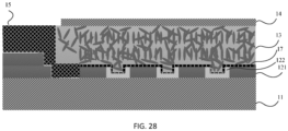
- 10 - high contrast grating polarizer with adjustable polarization characteristics 11 - transparent substrate, 12 - plasma metal antenna structure layer, 121 - high contrast grating, 122 - plasma metal antenna structure, 13 - refractive index electrically-tunable switching layer, 14 - first electrode layer, 15 - second electrode layer, 16 - protective glass, 17 - protective layer.
- FIGs. 1 to 28 For ease of understanding and explanation, a high contrast grating polarizer with adjustable polarization characteristics, provided by the embodiments of the present disclosure, is detailed in detail below through FIGs. 1 to 28 .
- the high contrast grating polarizer 10 includes a transparent substrate 11, and a plasma metal antenna structure layer 12 , a refractive index electrically-tunable switching layer 13, a first electrode layer 14 and a second electrode layer 15 located on the transparent substrate 11, where the plasma metal antenna structure layer 12 may include a high contrast grating (HCG) 121 and a plasma metal antenna structure 122 interleaved with the high contrast grating 121, the high contrast grating 121 includes but is not limited to a semiconductor grating or a dielectric grating, the high contrast grating 121 can transmit light in a first polarization direction, the plasma metal antenna structure 122 can reflect light in a second polarization direction, and the first polarization direction is opposite to the second polarization direction.
- HCG high contrast grating
- polarized light includes but is not limited to S polarized light, P polarized light, circularly polarized light, elliptically polarized light, and the like.
- the polarization characteristics include but are not limited to polarization direction, transmittance, extinction ratio, polarization type, and the like.
- Transmitted light is mainly linearly polarized parallel to a high contrast grating strip
- reflected light is mainly polarized perpendicular to the high contrast grating strip.
- the transparent substrate 11 in the embodiment of the present disclosure may be made of one or more materials that are substantially transparent at working wavelengths of the polarizer.
- the working wavelengths include but are not limited to EUV (extreme ultraviolet), DUV (deep ultraviolet), UV (ultraviolet), VIS (visible), NIR (near infrared), MIR (mid infrared), FIR (far infrared), THz (terahertz), or the like;
- the materials include but are not limited to SiO 2 (silicon dioxide), Al 2 O 3 (aluminum oxide), Si (silicon), or the like; or the transparent substrate 11 may be various types of glass substrates, amorphous substrates, polycrystalline substrates, crystalline substrates or the like.
- the high contrast grating 121 includes but is not limited to a semiconductor grating or a dielectric grating, such as made of Si (silicon), SiN (silicon nitride), Al 2 O 3 (aluminum oxide), or any other type of nonconductive material.
- the plasma metal antenna structure 122 may be made of any type of metal, such as Au (gold), Ag (silver), Al (aluminum), Fe (iron), alloy, or other conductive materials.
- the refractive index electrically-tunable switching layer 13 in the embodiment of the present disclosure includes but is not limited to a liquid crystal (LC) layer or the like.
- Liquid crystal is a state of matter with properties between conventional liquid and solid crystals.
- LC may form a medium with anisotropic optical properties.
- incident light corresponds to an extraordinary refractive index n e
- incident light corresponds to an ordinary refractive index n o .
- Liquid crystal molecules can be reoriented through an electric or magnetic field, and their effective birefringence changes accordingly. Therefore, as the applied electric or magnetic field changes, the incident light undergoes different phase delays.
- LC can form a medium with isotropic optical properties.
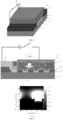
- FIG. 4(a) is a schematic diagram illustrating that P polarized light is incident on the high contrast grating polarizer to which external voltage is not applied, where the P polarized light means that an electric field direction of the light is perpendicular to the grating.
- the electric field direction of the light is perpendicular, the light will significantly interact with the metal, especially two side walls, so that the electric field cannot penetrate the metal but will be reflected. The two side walls reflect the electric field, the two electric fields will interfere with each other, and the cavity will work as an antenna resonator.
- FIG. 4(a) is a schematic diagram illustrating that P polarized light is incident on the high contrast grating polarizer to which external voltage is not applied, where the P polarized light means that an electric field direction of the light is perpendicular to the grating.
- the electric field direction of the light is perpendicular, the light will significantly interact with the metal, especially two side walls, so that the electric field cannot penetrate the metal but will be reflected.
- FIG. 4(b) illustrates a schematic diagram of electric field simulation of P polarized light with ⁇ equal to 0 degree according to an embodiment of the present disclosure, where the light is reflected and cannot pass through this structure.
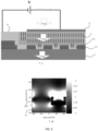
- FIG. 5(a) is a schematic diagram illustrating that P polarized light is incident on the high contrast grating polarizer to which external voltage is applied. Due to the effect of the external voltage, the orientation of liquid crystal follows a direction, resulting in changes in the refractive index of the surrounding environment. Even though the interaction between light and metal is significant, most of the light will leak through the grating and exhibit high transmittance due to phase mismatch.
- FIG. 5(b) illustrates a schematic diagram of electric field simulation of P polarized light with ⁇ equal to 0 degree according to an embodiment of the present disclosure, where the light passes through the grating.
- FIG. 6(a) is a schematic diagram illustrating that S polarized light is incident on the high contrast grating polarizer to which external voltage is not applied, where the S polarized light means that an electric field direction of the light is parallel to the grating.
- the S polarized light means that an electric field direction of the light is parallel to the grating.
- a reflection phase from a top of the grating and a reflection phase from a bottom of the grating are different by designing a specific period, duty cycle and grating thickness, thereby suppressing light reflection under specific design conditions.
- FIG. 6(b) illustrates a schematic diagram of electric field simulation of S polarized light with ⁇ equal to 0 degree according to an embodiment of the present disclosure, where the light passes through the grating.
- FIG. 7(a) is a schematic diagram illustrating that S polarized light is incident on the high contrast grating polarizer to which external voltage is applied. Due to the effect of the external voltage, the orientation of liquid crystal follows a direction, resulting in changes in the refractive index of the surrounding environment. However, most of the S polarized light passes through this structure.
- FIG. 7(b) illustrates a schematic diagram of electric field simulation of S polarized light with ⁇ equal to 0 degree according to an embodiment of the present disclosure, where the light passes through the grating.
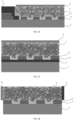
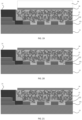
- FIG. 8 to FIG. 11 are schematic diagrams illustrating that different external voltages are applied to the high contrast grating polarizer, respectively, where a relationship among the different external voltages is V0 ⁇ V1 ⁇ V2 ⁇ V3. From the figures, it can be seen that, when a higher voltage is applied, more liquid crystals follow the electric field direction. It should be noted that the refractive index of at least one material in the switching layer 13 of the high contrast grating polarizer 10 is changed by applying continuous voltage, electric field, current, or magnetic field (or a combination thereof).
- the change in refractive index can be substantially isotropic or anisotropic, the change in refractive index can further change the material from an isotropic refractive index to an anisotropic refractive index, and liquid crystals exhibit in the latter way.
- the change in refractive index can be continuous or abrupt, and electric bias can be applied in a gradient or abrupt manner, so the polarization characteristics can be switched gradually or suddenly.
- the gradient manner includes (1) implementing a gradual change in transmission of light in a polarization direction, and maintaining transmission of light in an opposite polarization direction to a great extent; (2) implementing a gradual change in reflection of light in a polarization direction, and maintaining reflection of light in an opposite polarization direction to a great extent; and (3) tuning an extinction ratio of the polarizer from a higher value to a lower value, and vice versa.
- the abrupt manner includes (1) switching from a state in which light in a polarization state has high transmission to a state in which light in an opposite polarization state has high transmission, (2) switching from a state in which light in a polarization state has high reflection to a state in which light in an opposite polarization state has high reflection, (3) switching from a state in which light in a polarization state has high transmissivity to a state in which light in two polarization states has high transmissivity, and (4) switching from a state in which light in a polarization state has high reflectivity to a state in which light in two polarization states has high reflectivity.
- the high contrast grating polarizer 10 in the embodiment of the present disclosure may be of a periodic or non-periodic structure.
- the high contrast grating polarizer 10 may be of a one-dimensional or two-dimensional structure.
- the plasma metal antenna structure layer 12 has a periodic structure in length and width directions of the transparent substrate 11 (as shown in FIG.
- the plasma metal antenna structure layer 12 has a periodic structure in the length direction of the transparent substrate 11 and a non-periodic structure in the width direction of the transparent substrate 11 (as shown in FIG. 13 ), and these structures may be used for linear polarizers and beam splitters; or the plasma metal antenna structure layer 12 has a periodic structure in the width direction of the transparent substrate 11 and a non-periodic structure in the length direction of the transparent substrate 11; or the plasma metal antenna structure layer 12 has a non-periodic structure in the length and width directions of the transparent substrate 11 (as shown in FIG.
- this structure may be used for linear polarizers, circular polarizers, elliptical polarizers, and beam splitters.
- a one-dimensional or two-dimensional grating structure with a specific preferred transverse direction is beneficial to the application of a polarizer commonly used as a linear polarizer.
- the preferred transverse direction of a grating element is perpendicular or parallel to the polarization of incident light.
- a two-dimensional grating structure with chiral symmetry is a preferred embodiment, where the polarizer is commonly used as a circular polarizer.
- the grating of the polarizer preferably has a period less than a specific value related to the wavelength of light to prevent diffraction loss.
- the refractive index electrically-tunable switching layer 13 is located between the high contrast grating 121 and the plasma metal antenna structure 122 (as shown in FIG. 1 , etc.); or the refractive index electrically-tunable switching layer 13 is located below the plasma metal antenna structure layer 12.
- Such setting can effectively switch the optical characteristics of the high contrast grating polarizer 10, with high sensitivity and high reliability.
- the first electrode layer 14 is located above the refractive index electrically-tunable switching layer 13, and the second electrode layer 15 is connected to the plasma metal antenna structure 122 (as shown in FIG. 16 , etc.); or the first electrode layer 14 is located above the refractive index electrically-tunable switching layer 13, and the second electrode layer 15 is located below the plasma metal antenna structure layer 12 (as shown in FIG. 17 ); or the first electrode layer 14 is located on a left side of the refractive index electrically-tunable switching layer 13, and the second electrode layer 15 is located on a right side of the refractive index electrically-tunable switching layer 13 (as shown in FIG. 18 ).
- both the first electrode layer 14 and the second electrode layer 15 are transparent conductive films; or the first electrode layer 14 is a transparent conductive film, and the second electrode layer 15 is a portion of the plasma metal antenna structure 122.
- the transparent conductive film includes but is not limited to ITO (tin-doped indium oxide) glass and FTO (fluorine-doped tin oxide) glass, and a portion of the plasma metal antenna structure 122 may be an Au (gold) contact electrode.
- protective glass 16 (as shown in FIG. 19 ) may be further provided on the first electrode layer 14 to effectively protect the high contrast grating polarizer 10 and prolong its service life.
- the plasma metal antenna structure 122 is located in at least one position among a bottom, a left wall, and a right wall of a high contrast grating gap.
- the plasma metal antenna structure 122 is located at the bottom, left wall, and right wall of the high contrast grating gap (as shown in FIG. 1 , etc.); or the plasma metal antenna structure 122 is located at the bottom and left wall of the high contrast grating gap (as shown in FIG. 20 ); or the plasma metal antenna structure 122 is located at the bottom and right wall of the high contrast grating gap (as shown in FIG. 21 ); or the plasma metal antenna structure 122 is located at the bottom of the high contrast grating gap (as shown in FIG. 22 ).
- the plasma metal antenna structure 122 is located in at least one position among a top, a left wall, and a right wall of each high contrast grating strip.
- the plasma metal antenna structure 122 is located at the top of each high contrast grating strip (as shown in FIG. 23 ); or the plasma metal antenna structure 122 is located at the top, left wall, and right wall of each high contrast grating strip (as shown in FIG. 24 ); or the plasma metal antenna structure 122 is located on the left and right walls of each high contrast grating strip (as shown in FIG. 25 ); or the plasma metal antenna structure 122 is located on the right wall of each high contrast grating strip (as shown in FIG. 26 ); or the plasma metal antenna structure 122 is located on the left wall of each high contrast grating strip (as shown in FIG. 27 ).
- a first bonding layer is provided between the transparent substrate 11 and the high contrast grating 121, thereby enhancing adhesion of the high contrast grating 121.
- the first bonding layer may include any of a SiN layer, an Al 2 O 3 layer, and a SiO 2 layer.
- the first bonding layer may be deposited by ALD (Atomic Layer Deposition), PECVD (Plasma Enhanced Chemical Vapor Deposition), CVD (Chemical Vapor Deposition), PVD (Physical Vapor Deposition), or the like.
- a second bonding layer is further provided between the transparent substrate 11 and the plasma metal antenna structure 122, and/or between the high contrast grating 121 and the plasma metal antenna structure 122, thereby enhancing adhesion of a metal surface.
- the second bonding layer may include any of a Ti (titanium) layer, a Ge (germanium) layer, and an Al (aluminum) layer.
- the second bonding layer may be deposited by ALD, PECVD, CVD, PVD, sputtering, or the like.
- a protective layer 17 is provided between the plasma metal antenna structure layer 12 and the refractive index electrically-tunable switching layer 13, thereby improving manufacturability, reliability, and performance of the high contrast grating polarizer 10.
- the protective layer 17 may include any of a SiN layer, an Al 2 O 3 layer, and a SiO 2 layer, and may be deposited by ALD, PECVD, CVD, PVD, or the like.
- a metal adjacent to a grating side wall, a metal adjacent to another grating side wall, a metal at a bottom of a grating gap, and a metal at a top of a grating may have different thicknesses.
- a ratio of the thickness of the side wall metal to the thickness of the bottom metal may be greater than 0.2 and less than 3.
- the metal layer may be discontinuous, that is, there may be pores, and the discontinuous size should be less than the distance between two gratings.
- the plasma metal antenna structure layer is combined with the refractive index electrically-tunable switching layer to change the refractive index of the switching layer in an electrical tuning manner such as an electric or magnetic field, thereby affecting the transmissivity and reflectivity of opposite polarized light, changing the polarization characteristics of the polarizer, and making the polarizer efficient, convenient, responsive, and highly reliable.
Landscapes
- Physics & Mathematics (AREA)
- General Physics & Mathematics (AREA)
- Optics & Photonics (AREA)
- Nonlinear Science (AREA)
- Chemical & Material Sciences (AREA)
- Crystallography & Structural Chemistry (AREA)
- Polarising Elements (AREA)
Applications Claiming Priority (2)
| Application Number | Priority Date | Filing Date | Title |
|---|---|---|---|
| CN202310727896.2A CN117170004A (zh) | 2023-06-16 | 2023-06-16 | 一种偏振特性可调的高对比度光栅偏振器 |
| CN202321552868.3U CN220381310U (zh) | 2023-06-16 | 2023-06-16 | 一种偏振特性可调的高对比度光栅偏振器 |
Publications (1)
| Publication Number | Publication Date |
|---|---|
| EP4478097A1 true EP4478097A1 (de) | 2024-12-18 |
Family
ID=89223726
Family Applications (1)
| Application Number | Title | Priority Date | Filing Date |
|---|---|---|---|
| EP23217678.4A Pending EP4478097A1 (de) | 2023-06-16 | 2023-12-18 | Kontraststarker gitterpolarisator mit einstellbarer polarisationscharakteristik |
Country Status (2)
| Country | Link |
|---|---|
| US (1) | US20240418918A1 (de) |
| EP (1) | EP4478097A1 (de) |
Citations (1)
| Publication number | Priority date | Publication date | Assignee | Title |
|---|---|---|---|---|
| KR20080040067A (ko) * | 2006-11-02 | 2008-05-08 | 삼성전자주식회사 | 편광판, 이를 갖는 표시패널 및 표시장치 |
-
2023
- 2023-11-14 US US18/508,772 patent/US20240418918A1/en active Pending
- 2023-12-18 EP EP23217678.4A patent/EP4478097A1/de active Pending
Patent Citations (1)
| Publication number | Priority date | Publication date | Assignee | Title |
|---|---|---|---|---|
| KR20080040067A (ko) * | 2006-11-02 | 2008-05-08 | 삼성전자주식회사 | 편광판, 이를 갖는 표시패널 및 표시장치 |
Also Published As
| Publication number | Publication date |
|---|---|
| US20240418918A1 (en) | 2024-12-19 |
Similar Documents
| Publication | Publication Date | Title |
|---|---|---|
| US10473839B2 (en) | Reflective LC devices including thin film metal grating | |
| CN113376870B (zh) | 一种基于相变材料的空间光型电光调制器件及其制造方法 | |
| US11804656B2 (en) | Reconfigurable geometric metasurfaces with optically tunable materials | |
| KR100744863B1 (ko) | 가시 광선 대역에 대한 삽입형 와이어 격자 편광자 | |
| EP3570081A1 (de) | Mehrschicht-drahtgitterpolarisator | |
| Ahmed et al. | Novel design of wide temperature ranges sensor based on Tamm state in a pyroelectric photonic crystal with high sensitivity | |
| WO2015077127A1 (en) | High reflectivity lcos device | |
| US10222675B2 (en) | Thin film plasmonic optical modulator | |
| US12487468B2 (en) | Reflection-asymmetric metal grating polarization beam splitter | |
| CN113267901A (zh) | 基于各向异性手性超材料的动态偏振调控器件 | |
| Hutchings et al. | Theory of optical bistability in metal mirrored Fabry-Perot cavities containing thermo-optic materials | |
| CN101661185B (zh) | 液晶光衰减装置 | |
| WO2022222638A1 (zh) | 一种用于控制电磁波的装置 | |
| EP4478097A1 (de) | Kontraststarker gitterpolarisator mit einstellbarer polarisationscharakteristik | |
| CN112394543A (zh) | 一种基于铌酸锂薄膜的可调谐fp滤光片 | |
| EP0696362B1 (de) | Optische vorrichtungen | |
| CN220381310U (zh) | 一种偏振特性可调的高对比度光栅偏振器 | |
| JP7738339B2 (ja) | 偏光特性を調整可能な高コントラストグレーチング偏光子 | |
| CN220105331U (zh) | 一种高对比度光栅偏振片 | |
| CN108761617A (zh) | 介质腔增强型高反射波片及其制备方法 | |
| EP4439134B1 (de) | Kontrastreiches gitterpolarisator | |
| KR102914080B1 (ko) | 유전체 금속 듀얼 와이어 그리드 기반의 광대역 파장판 및 그 제조 방법 | |
| JP3897300B2 (ja) | 液晶情報ディスプレイ | |
| Kupreychik et al. | Infrared Acousto-Optic Filters Based on a Biaxial Crystal of Indium Iodide for Combined Spectral-Polarization Analysis of Optical Images | |
| Shen et al. | Guided-mode resonant grating filter based on Sb2Se3 with dual-band tuning |
Legal Events
| Date | Code | Title | Description |
|---|---|---|---|
| PUAI | Public reference made under article 153(3) epc to a published international application that has entered the european phase |
Free format text: ORIGINAL CODE: 0009012 |
|
| STAA | Information on the status of an ep patent application or granted ep patent |
Free format text: STATUS: REQUEST FOR EXAMINATION WAS MADE |
|
| 17P | Request for examination filed |
Effective date: 20231227 |
|
| AK | Designated contracting states |
Kind code of ref document: A1 Designated state(s): AL AT BE BG CH CY CZ DE DK EE ES FI FR GB GR HR HU IE IS IT LI LT LU LV MC ME MK MT NL NO PL PT RO RS SE SI SK SM TR |