EP4475634A1 - Composite wiring board, electronic component storage package, and electronic device - Google Patents
Composite wiring board, electronic component storage package, and electronic device Download PDFInfo
- Publication number
- EP4475634A1 EP4475634A1 EP23747027.3A EP23747027A EP4475634A1 EP 4475634 A1 EP4475634 A1 EP 4475634A1 EP 23747027 A EP23747027 A EP 23747027A EP 4475634 A1 EP4475634 A1 EP 4475634A1
- Authority
- EP
- European Patent Office
- Prior art keywords
- signal line
- wiring board
- slit
- composite wiring
- board according
- Prior art date
- Legal status (The legal status is an assumption and is not a legal conclusion. Google has not performed a legal analysis and makes no representation as to the accuracy of the status listed.)
- Withdrawn
Links
Images





Classifications
-
- H—ELECTRICITY
- H05—ELECTRIC TECHNIQUES NOT OTHERWISE PROVIDED FOR
- H05K—PRINTED CIRCUITS; CASINGS OR CONSTRUCTIONAL DETAILS OF ELECTRIC APPARATUS; MANUFACTURE OF ASSEMBLAGES OF ELECTRICAL COMPONENTS
- H05K3/00—Apparatus or processes for manufacturing printed circuits
- H05K3/36—Assembling printed circuits with other printed circuits
- H05K3/361—Assembling flexible printed circuits with other printed circuits
- H05K3/363—Assembling flexible printed circuits with other printed circuits by soldering
-
- H—ELECTRICITY
- H05—ELECTRIC TECHNIQUES NOT OTHERWISE PROVIDED FOR
- H05K—PRINTED CIRCUITS; CASINGS OR CONSTRUCTIONAL DETAILS OF ELECTRIC APPARATUS; MANUFACTURE OF ASSEMBLAGES OF ELECTRICAL COMPONENTS
- H05K1/00—Printed circuits
- H05K1/02—Details
- H05K1/0277—Bendability or stretchability details
-
- H—ELECTRICITY
- H05—ELECTRIC TECHNIQUES NOT OTHERWISE PROVIDED FOR
- H05K—PRINTED CIRCUITS; CASINGS OR CONSTRUCTIONAL DETAILS OF ELECTRIC APPARATUS; MANUFACTURE OF ASSEMBLAGES OF ELECTRICAL COMPONENTS
- H05K1/00—Printed circuits
- H05K1/02—Details
- H05K1/0213—Electrical arrangements not otherwise provided for
-
- H—ELECTRICITY
- H05—ELECTRIC TECHNIQUES NOT OTHERWISE PROVIDED FOR
- H05K—PRINTED CIRCUITS; CASINGS OR CONSTRUCTIONAL DETAILS OF ELECTRIC APPARATUS; MANUFACTURE OF ASSEMBLAGES OF ELECTRICAL COMPONENTS
- H05K1/00—Printed circuits
- H05K1/02—Details
- H05K1/0213—Electrical arrangements not otherwise provided for
- H05K1/0216—Reduction of cross-talk, noise or electromagnetic interference
- H05K1/0218—Reduction of cross-talk, noise or electromagnetic interference by printed shielding conductors, ground planes or power plane
- H05K1/0224—Patterned shielding planes, ground planes or power planes
- H05K1/0225—Single or multiple openings in a shielding, ground or power plane
-
- H—ELECTRICITY
- H05—ELECTRIC TECHNIQUES NOT OTHERWISE PROVIDED FOR
- H05K—PRINTED CIRCUITS; CASINGS OR CONSTRUCTIONAL DETAILS OF ELECTRIC APPARATUS; MANUFACTURE OF ASSEMBLAGES OF ELECTRICAL COMPONENTS
- H05K1/00—Printed circuits
- H05K1/02—Details
- H05K1/14—Structural association of two or more printed circuits
- H05K1/147—Structural association of two or more printed circuits at least one of the printed circuits being bent or folded, e.g. by using a flexible printed circuit
-
- H—ELECTRICITY
- H05—ELECTRIC TECHNIQUES NOT OTHERWISE PROVIDED FOR
- H05K—PRINTED CIRCUITS; CASINGS OR CONSTRUCTIONAL DETAILS OF ELECTRIC APPARATUS; MANUFACTURE OF ASSEMBLAGES OF ELECTRICAL COMPONENTS
- H05K1/00—Printed circuits
- H05K1/18—Printed circuits structurally associated with non-printed electric components
- H05K1/189—Printed circuits structurally associated with non-printed electric components characterised by the use of flexible or folded printed circuits
-
- H—ELECTRICITY
- H05—ELECTRIC TECHNIQUES NOT OTHERWISE PROVIDED FOR
- H05K—PRINTED CIRCUITS; CASINGS OR CONSTRUCTIONAL DETAILS OF ELECTRIC APPARATUS; MANUFACTURE OF ASSEMBLAGES OF ELECTRICAL COMPONENTS
- H05K1/00—Printed circuits
- H05K1/02—Details
- H05K1/0213—Electrical arrangements not otherwise provided for
- H05K1/0216—Reduction of cross-talk, noise or electromagnetic interference
- H05K1/0218—Reduction of cross-talk, noise or electromagnetic interference by printed shielding conductors, ground planes or power plane
- H05K1/0219—Printed shielding conductors for shielding around or between signal conductors, e.g. coplanar or coaxial printed shielding conductors
-
- H—ELECTRICITY
- H05—ELECTRIC TECHNIQUES NOT OTHERWISE PROVIDED FOR
- H05K—PRINTED CIRCUITS; CASINGS OR CONSTRUCTIONAL DETAILS OF ELECTRIC APPARATUS; MANUFACTURE OF ASSEMBLAGES OF ELECTRICAL COMPONENTS
- H05K1/00—Printed circuits
- H05K1/02—Details
- H05K1/0213—Electrical arrangements not otherwise provided for
- H05K1/0237—High frequency adaptations
- H05K1/0245—Lay-out of balanced signal pairs, e.g. differential lines or twisted lines
-
- H—ELECTRICITY
- H05—ELECTRIC TECHNIQUES NOT OTHERWISE PROVIDED FOR
- H05K—PRINTED CIRCUITS; CASINGS OR CONSTRUCTIONAL DETAILS OF ELECTRIC APPARATUS; MANUFACTURE OF ASSEMBLAGES OF ELECTRICAL COMPONENTS
- H05K1/00—Printed circuits
- H05K1/02—Details
- H05K1/11—Printed elements for providing electric connections to or between printed circuits
- H05K1/118—Printed elements for providing electric connections to or between printed circuits specially for flexible printed circuits, e.g. using folded portions
-
- H—ELECTRICITY
- H05—ELECTRIC TECHNIQUES NOT OTHERWISE PROVIDED FOR
- H05K—PRINTED CIRCUITS; CASINGS OR CONSTRUCTIONAL DETAILS OF ELECTRIC APPARATUS; MANUFACTURE OF ASSEMBLAGES OF ELECTRICAL COMPONENTS
- H05K2201/00—Indexing scheme relating to printed circuits covered by H05K1/00
- H05K2201/09—Shape and layout
- H05K2201/09009—Substrate related
- H05K2201/09063—Holes or slots in insulating substrate not used for electrical connections
-
- H—ELECTRICITY
- H10—SEMICONDUCTOR DEVICES; ELECTRIC SOLID-STATE DEVICES NOT OTHERWISE PROVIDED FOR
- H10W—GENERIC PACKAGES, INTERCONNECTIONS, CONNECTORS OR OTHER CONSTRUCTIONAL DETAILS OF DEVICES COVERED BY CLASS H10
- H10W76/00—Containers; Fillings or auxiliary members therefor; Seals
- H10W76/60—Seals
Definitions
- the present disclosure relates to a composite wiring board, an electronic component accommodating package, and an electronic device.
- WO 2019/050046 A discloses a structure for connection between an electronic component accommodating package and a flexible substrate.
- a composite wiring board includes a wiring board, and a flexible substrate.
- the wiring board includes a first joint region.
- the flexible substrate includes a second joint region overlapped with the first joint region.
- the wiring board includes a first signal line, and a cutout disposed adjacent to the first signal line.
- the flexible substrate includes a second signal line to be joined to the first signal line, and a slit disposed adjacent to the second signal line.
- the cutout is positioned in the first joint region in a plan perspective view.
- the slit is positioned in the second joint region in a plan perspective view.
- an electronic component accommodating package includes the composite wiring board and a frame positioned on the wiring board.
- an electronic device includes the electronic component accommodating package and an electronic component positioned inside the frame.
- FIG. 1A is a perspective view illustrating a principal part of a composite wiring board according to embodiment 1 of the present disclosure.
- FIG. 1B is a rear-side perspective view illustrating the principal part of the composite wiring board according to embodiment 1 of the present disclosure.
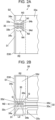
- FIGs. 2A and 2B are a front-side plan view and a rear-side plan view each illustrating a principal part of a flexible substrate.
- FIG. 3 is a plan view illustrating a principal part of a wiring board.
- Embodiment 1 provides a composite wiring board 10 including a wiring board 20 and a flexible substrate 30.
- the wiring board 20 includes an insulating substrate 21, a first signal line 22 positioned on the insulating substrate 21, and a recess 24 provided as a cutout.
- the recess 24 is disposed adjacent to the first signal line 22.
- the first signal line 22 and the recess 24 adjacent to each other are aligned in a line width direction of the first signal line 22, a line direction, or in a direction slanted from the line width direction.
- a center line in the line direction of the first signal line 22 and a center line in a longitudinal direction of the recess 24 may be parallel or nonparallel to each other.
- the recess 24 may be positioned around the first signal line 22. Being positioned around the first signal line 22 can mean being positioned close enough to influence transmission characteristics of the first signal line 22, and can mean that distance from the first signal line 22 is twice or less a line width of the first signal line 22.
- the wiring board 20 may further include a ground conductor 23 positioned on the insulating substrate 21.
- the insulating substrate 21 may be made of a ceramic or a resin.
- FIGs. 1 to 5 exemplarily illustrate the wiring board 20 integrated with a frame 52. Alternatively, the frame 52 may be removed.
- the insulating substrate 21 may have a plate shape without the frame 52.
- the frame 52 may be formed integrally with the wiring board 20, or may be formed separately and joined to the wiring board 20.
- the insulating substrate 21 and the frame 52 may interpose a different member.
- the first signal line 22 is a signal line configured to transmit a radio-frequency signal.
- the first signal line 22 may be single-ended as a single signal line, or may include two signal lines, namely, a 1a-th signal line 22a and a 1b-th signal line 22b.
- the 1a-th signal line 22a and the 1b-th signal line 22b may be parallel to each other.
- the 1a-th signal line 22a and the 1b-th signal line 22b may be signal lines each configured to transmit a differential signal.
- the first signal line 22 (i.e., the 1a-th signal line 22a and the 1b-th signal line 22b) may be positioned on an upper surface of the insulating substrate 21. Part of the first signal line 22 may be positioned on the upper surface of the insulating substrate 21 whereas the remaining part may be positioned inside the insulating substrate 21 or on a rear surface of the insulating substrate 21. When the frame 52 is provided, part of the first signal line 22 may be positioned inside the frame 52 (e.g., between the frame 52 and the insulating substrate 21).
- the recess 24 may be positioned between the 1a-th signal line 22a and the 1b-th signal line 22b.
- the recess 24 may be shaped to be oblong along the signal line.
- the recess 24 may have an oval shape or a rectangular shape in a plan perspective view.
- Plan perspective view means perspectively viewing in a direction vertical to a board surface of the wiring board 20 provided with the first signal line 22.
- the recess 24 may be opened to the board surface.
- the recess 24 may have a tapered shape, an inversely tapered shape, or a stepped shape in a sectional view.
- the recess 24 in the tapered shape includes an open end wider than a bottom end, whereas the recess 24 in the inversely tapered shape includes the bottom end wider than the open end.
- the recess 24 may be distant from or in contact with the 1a-th signal line 22a and the 1b-th signal line 22b.
- the ground conductor 23 may include ground film conductors 23a and 23b (see FIG. 3 ) positioned on respective sides of the first signal line 22 (i.e., the 1a-th signal line 22a and the 1b-th signal line 22b), a ground film conductor 23c (see FIG. 3 ) positioned on a bottom surface of the recess 24, a ground film conductor 23d (see FIG. 1A ) expanding in a layer below the first signal line 22, a ground film conductor 23e (see FIG. 1A ) expanding in a layer above the first signal line 22 inside the frame 52 when the frame 52 is provided, a ground via conductor 23v1 (see FIG.
- the ground conductor 23 may further include a ground line 23h (see FIG. 3 ) positioned between the 1a-th signal line 22a and the 1b-th signal line 22b, and a ground via conductor (not illustrated) configured to provide conductivity between the ground line 23h and the ground film conductor 23d or 23e positioned in the lower or upper layer.
- the ground film conductors 23a and 23b may have film shapes expanding along the signal line and in the line width direction of the signal line with a clearance from the first signal line 22 (i.e., the 1a-th signal line 22a and the 1b-th signal line 22b).
- the ground line 23h may be positioned between the 1a-th signal line 22a and the 1b-th signal line 22b outside a region provided with the recess 24.
- the wiring board 20 includes a first joint region R1 overlapped with the flexible substrate 30.
- the wiring board 20 may include a first edge E20 disposed at one end of the board surface and crossing an extension of the first signal line 22, and the first joint region R1 may include the first edge E20.
- the first joint region R1 may expand to a foot of the frame 52. That is, the frame 52 and an edge of the flexible substrate 30 may be in contact with each other.
- the first joint region R1 may include part of the first signal line 22 (i.e., the 1a-th signal line 22a and the 1b-th signal line 22b), the recess 24, part of the ground film conductors 23a and 23b, and the ground film conductor 23c, which are mentioned above.
- Part including line ends of the 1a-th signal line 22a and the 1b-th signal line 22b may be positioned in the first joint region R1.
- An end of the 1a-th signal line 22a and an end of the 1b-th signal line 22b may be spaced apart from the first edge E20.
- the 1a-th signal line 22a and the 1b-th signal line 22b may be exposed onto the first joint region R1.
- the recess 24 may entirely be positioned in the first joint region R1.
- the ground film conductors 23a and 23b may expand in the first joint region R1 from the first edge E20 to an opposite edge. That is, the ground film conductors 23a and 23b may each extend from the first edge E20 to a position overlapped with a second edge E30 of the flexible substrate 30 in a plan perspective view.
- an interval between the two ground film conductors 23a and 23b positioned to interpose the first signal line 22 (specifically, an interval in the line width direction of the signal line) may be narrow near the first edge E20, wide in a center portion of the first joint region R1, and narrow at the opposite edge of the first edge E20.
- the ground film conductors 23a and 23b may be exposed onto the first joint region R1.
- the ground film conductor 23c may be positioned on the bottom surface of the recess 24.
- the bottom surface of the recess 24 and the ground film conductor 23c may be covered from above with an insulating film 25.
- the insulating film 25 may be alumina coating.
- the first signal line 22 or the recess 24 may be in contact with the first edge E20.
- the recess 24 may be opened to an end surface of the wiring board 20.
- the recess 24 may be a hole penetrating from an upper surface to a lower surface of the wiring board 20.
- the flexible substrate 30 may include an insulating base 31 having flexibility and a sheet shape.
- the insulating base 31 includes a first surface S1 and a second surface S2 positioned opposite to the first surface S1.
- the flexible substrate 30 includes a second signal line 32 positioned on the first surface S1.
- the second signal line 32 may partially be joined to the first signal line 22 on the wiring board 20, and may be equal in number of lines to the first signal line 22.
- the second signal line 32 may therefore include two signal lines, namely, a 2a-th signal line 32a and a 2b-th signal line 32b.
- the 2a-th signal line 32a and the 2b-th signal line 32b may be parallel to each other.
- the 2a-th signal line 32a and the 2b-th signal line 32b may be signal lines each configured to transmit a differential signal.
- the second signal line 32 may include electrode pads 32c and 32d larger in line width larger than the remaining part.
- the electrode pads 32c and 32d may be shaped to be oblong along the signal line, and may be positioned at an end of the second signal line 32.
- the flexible substrate 30 further includes a slit 35 disposed adjacent to the second signal line 32.
- the second signal line 32 and the slit 35 adjacent to each other are aligned in a line width direction of the second signal line 32, a line direction, or in a direction slanted from the line width direction.
- a center line in the line direction of the second signal line 32 and a center line in a longitudinal direction of the slit 35 are not necessarily parallel to each other.
- the slit 35 may be positioned around the second signal line 32.
- the slit 35 may be positioned from the first surface S1 to the second surface S2.
- the slit 35 may be hollow.
- the slit 35 may have a rectangular shape, a circular shape, an oblong shape, an elliptical shape, or the like.
- the slit 35 has a width that may be increased as being away from the second edge E30 or may inversely be decreased as being away from the second edge E30.
- the slit 35 may have a tapered shape, an inversely tapered shape, or a stepped shape in a sectional view.
- the tapered shape has a slanted side surface with a size at a level of the second surface S2 being larger than a size at a level of the first surface S1.
- the inversely tapered shape has a slanted side surface with a size at the level of the second surface S2 being smaller than a size at the level of the first surface S1.
- the slit 35 may be distant from or in contact with the second signal line 32.
- the flexible substrate 30 may further include a film conductor positioned on the first surface S1 and the second surface S2, and a via conductor positioned from the first surface S1 to the second surface S2, which are to be described later.
- the film conductor may include electrode film conductors 33a and 33b positioned on the second surface S2, a second ground film conductor 33e positioned on the second surface S2, and first ground film conductors 33c and 33d positioned on respective sides to interpose the second signal line 32 on the first surface S1.
- the electrode film conductors 33a and 33b may be positioned to face the electrode pads 32c and 32d of the second signal line 32.
- the second ground film conductor 33e may expand around the electrode film conductors 33a and 33b with a clearance to surround the electrode film conductors 33a and 33b from three sides.
- the three sides include both sides of a line width direction of a signal line and a side along the signal line.
- the via conductor may include electrode via conductors 34a to 34d connecting the electrode pads 32c and 32d and the electrode film conductors 33a and 33b, and a plurality of ground via conductors (not illustrated) connecting the first ground film conductors 33c and 33d and the second ground film conductor 33e.
- the plurality of ground via conductors may interpose the 2a-th signal line 32a and the 2b-th signal line 32b and be aligned along the signal lines.
- the flexible substrate 30 includes a second joint region R2 overlapped with the first joint region R1 of the wiring board 20.
- the flexible substrate 30 may include the second edge E30 disposed at one end and crossing an extension of the second signal line 32, and the second joint region R2 may include the second edge E30.
- the second joint region R2 may be provided with the electrode pads 32c and 32d of the second signal line 32, part of the first ground film conductors 33c and 33d, and the slit 35.
- An opposite surface of the second joint region R2 may be provided with the electrode film conductors 33a and 33b, part of the second ground film conductor 33e, and the slit 35.
- the electrode pads 32c and 32d, the first ground film conductors 33c and 33d, the electrode film conductors 33a and 33b, and the second ground film conductor 33e may be spaced apart from the second edge E30.
- the slit 35 may be positioned to reach the second edge E30.
- the electrode film conductors 33a and 33b have portions that are connected to the electrode via conductors 34a to 34d and that may be wider than the remaining portions. That is, the electrode film conductors 33a and 33b have outlines that may have uneven portions (specifically narrow concave portions and wide convex portions) N1 and N2 including portions projecting in the line width direction and portions depressed in the line width direction which are alternately aligned along the signal line.
- the second ground film conductor 33e may include uneven portions N3 and N4 including portions projecting in the line width direction and portions depressed in the line width direction which are alternately aligned in portions facing the electrode film conductors 33a and 33b in the line width direction of the signal line. Each of the projecting portions may be connected to the ground via conductor.
- the uneven portions N1 and N2 of the electrode film conductors 33a and 33b and the uneven portions N3 and N4 of the second ground film conductor 33e may be disposed staggeredly.
- the concave portions in the uneven portions N1 and N2 and the convex portions in the uneven portions N3 and N4 may be aligned in the line width direction, and the convex portions in the uneven portions N1 and N2 and the concave portions in the uneven portions N3 and N4 may be aligned in the line width direction.
- FIGs. 4A and 4B are a longitudinal sectional view and a plan view each illustrating a joint portion of the signal lines and the periphery of the joint portion.
- FIGs. 5A and 5B are sectional views taken along line A-A in FIG. 4B .
- FIGs. 5A and 5B illustrate an identical location.
- the first joint region R1 of the wiring board 20 and the second joint region R2 of the flexible substrate 30 are overlapped with each other.
- Part of the first joint region R1 and part of the second joint region R2 may be joined to each other via a bonding material F such as a brazing filler metal having electroconductivity (see FIGs. 4A , 5A, and 5B ).
- the first signal line 22 in the first joint region R1 and the electrode pads 32c and 32d in the second joint region R2 may be joined to each other via the bonding material F (that is, the second signal line 32 may be joined), and the ground film conductors 23a and 23b in the first joint region R1 and the first ground film conductors 33c and 33d (see FIG. 2B ) in the second joint region R2 may be joined to each other via the bonding material F.
- heat is applied to an opposite side of the second joint region R2 of the flexible substrate 30 in the state where the first joint region R1 and the second joint region R2 are overlapped with each other, to transfer heat to the bonding material F at each site via the conductors on the flexible substrate 30 and melt the bonding material F.
- the bonding material F is then cooled to be solidified, and the first joint region R1 and the second joint region R2 are joined to each other.
- the wiring board 20 includes the first signal line 22, and the recess 24 provided as a cutout and disposed adjacent to the first signal line 22.
- the flexible substrate 30 includes the second signal line 32, and the slit 35 disposed adjacent to the second signal line 32.
- the recess 24 is positioned in the first joint region R1 whereas the slit 35 is positioned in the second joint region R2 in a plan perspective view.
- This configuration can suppress an increase in the capacitance components (e.g., electrostatic capacitance components) around the joint portion between the first signal line 22 and the second signal line 32. That is, the joint portion is provided with the wiring board 20 and the insulating base 31 each having a high relative dielectric constant.
- the slit 35 thus provided can decrease a relative dielectric constant around the second signal line 32 on the insulating base 31.
- the joint portion can therefore have a suppressed increase in the capacitance components of the second signal line 32.
- the recess 24 thus provided can decrease a relative dielectric constant around the first signal line 22 on the insulating substrate 21.
- the joint portion can therefore have a suppressed increase in the capacitance components of the first signal line 22.
- the joint portion between the first signal line 22 and the second signal line 32 can have a suppressed possibility of an increase in capacitance components and improved characteristic impedance matching.
- the composite wiring board 10 can therefore be improved in radio-frequency signal transmission characteristics.
- the slit 35 may be positioned to reach the second edge E30 of the flexible substrate 30.
- This configuration can further suppress an increase in the capacitance components around the second signal line 32.
- the joint portion between the first signal line 22 and the second signal line 32 can therefore have an efficiently suppressed increase in capacitance components. Accordingly, the joint portion can have more improved characteristic impedance matching and more improved radio-frequency signal transmission characteristics.
- the second signal line 32 may include the 2a-th signal line 32a and the 2b-th signal line 32b disposed parallel to each other. As described above, and the slit 35 may be positioned between the 2a-th signal line 32a and the 2b-th signal line 32b. In this configuration, due to symmetry between the first signal line 22 and the second signal line 32, the first signal line 22 on the wiring board 20 includes the 1a-th signal line 22a and the 1b-th signal line 22b. Provision of the slit 35 as described above can achieve a suppress increase in the capacitance components between the 2a-th signal line 32a and the 2b-th signal line 32b. The joint portion between the first signal line 22 and the second signal line 32 can therefore have an efficiently suppressed increase in capacitance components and can be improved in radio-frequency signal transmission characteristics.
- the recess 24 provided as a cutout and the slit 35 may be at least partially overlapped with each other in a plan perspective view (see FIG. 4B ).
- This configuration can decrease capacitance components of the insulating substrate 21 and capacitance components of the insulating base 31 at symmetrical locations on the insulating substrate 21 and the insulating base 31. This can therefore achieve a decreased difference in characteristic impedance between the joint portion of the first signal line 22 and the second signal line 32 and locations in front of and behind the joint portion. This can therefore improve radio-frequency signal transmission characteristics.
- the recess 24 and the slit 35 are preferably overlapped with each other by 50% or more in area ratio in a plan perspective view (that is, in a plan perspective view, 50% or more of the total area of the recess 24 is overlapped with the slit 35, and 50% or more of the total area of the slit 35 is overlapped with the recess 24). Overlapping by 50% or more in area ratio can achieve a decrease in the capacitance components of the insulating substrate 21 and a decrease in the capacitance components of the insulating base 31.
- the slit 35 has a size L2 (see FIG. 2B ) in the direction along the signal line, and the size L2 may be larger than a size L1 (see FIG. 3 ) of the recess 24 in the direction.
- This configuration can stably secure an overlapping length between the slit 35 and the recess 24 even with any joined position error in the direction along the signal line.
- the joint portion can therefore have a stably suppressed increase in capacitance components and can stably be improved in radio-frequency signal transmission characteristics.
- the recess 24 has a width W1 (specifically a width in the line width direction of the signal line, see FIGs. 3 and 5A ) which may be larger than a width W2 of the slit 35 (specifically a width in the line width direction of the signal line, see FIGs. 2B and 5A ).
- This configuration can suppress overlapping between part of the first signal line 22 and the slit 35 even with any joined position error in the width direction of the signal line.
- the first j oint region R1 can thus stably achieve a structure in which the flexible substrate 30 overlaps on the first signal line 22. This structure can suppress large individual differences in characteristic impedance. This leads to stable radio-frequency signal transmission characteristics.
- the recess 24 has a thickness D1 (i.e., a length perpendicular to the board surface) which may be larger than a thickness D2 of the slit 35 (see FIG. 5A ).
- a thickness D1 i.e., a length perpendicular to the board surface
- the wiring board 20 can have a further suppressed increase in capacitance components.
- the composite wiring board 10 can therefore achieve stable radio-frequency signal transmission characteristics.
- the thickness D1 of the recess 24 may exemplarily be defined as the minimum distance from the board surface to the bottom surface of the recess 24.
- the size L2 (see FIG. 2B ) of the slit 35 may be larger than a size L3 (see FIG. 4B ) of a superimposed region M.
- the superimposed region M corresponds to a region where the first signal line 22 and the second signal line 32 are joined to each other (i.e., a region provided with the bonding material F) (see FIGs. 4B and 5B ).
- FIG. 4B illustrates the superimposed region M by hatching.
- the joint portion is likely to have a further decrease in the capacitance components around the second signal line 32. This can therefore more efficiently decrease the capacitance components and can improve radio-frequency signal transmission characteristics.
- the 1a-th signal line 22a has a line width W3 that may be smaller than a line width W4 of the 2a-th signal line 32a (specifically the width W4 of the electrode pad 32c) (see FIG. 5A ).
- This configuration can suppress extrusion of the 1a-th signal line 22a from the 2a-th signal line 32a (specifically the electrode pad 32c) in a plan perspective view even with any joined position error in the width direction of the signal line.
- the superimposed region M can thus stably achieve a structure in which the 2a-th signal line 32a (specifically the electrode pad 32c) overlaps on the 1a-th signal line 22a. This structure can suppress large individual differences in characteristic impedance. This leads to stable radio-frequency signal transmission characteristics.
- the line width W3 of the 1a-th signal line 22a may have the maximum size of the line width W3 of the 1a-th signal line 22a.
- the line width W3 of the 1b-th signal line 22b may be smaller than the line width W4 of the 2b-th signal line 32b (specifically the width W4 of the electrode pad 32d) (see FIG. 5A ).
- This configuration can suppress extrusion of the 1b-th signal line 22b from the 2b-th signal line 32b (specifically the electrode pad 32d) in a plan perspective view even with any joined position error in the width direction of the signal line.
- the superimposed region M can thus stably achieve a structure in which the 2b-th signal line 32b (specifically the electrode pad 32d) overlaps on the 1b-th signal line 22b. This structure can suppress large individual differences in characteristic impedance. This leads to stable radio-frequency signal transmission characteristics.
- the electrode film conductors (corresponding to first film conductors) 33a and 33b may be smaller in area than the superimposed region M (see FIG. 4B ). This configuration can also allow heat to be conducted from the second surface S2 to the electrode pads 32c and 32d positioned on the first surface S1 via the electrode film conductors 33a and 33b and allow the bonding material F to be melted. Furthermore, the electrode film conductors 33a and 33b having such small areas can decrease capacitance components generated by the electrode film conductors 33a and 33b in capacitance components to be applied to the second signal line 32. Therefore, the joint portion between the first signal line 22 and the second signal line 32 can have improved characteristic impedance matching and improved radio-frequency signal transmission characteristics.
- the slit 35 includes a first slit end portion t35 (see FIG. 4B ) positioned far from the second edge E30 of the flexible substrate 30.
- the first slit end portion t35 may be spaced apart from the first edge E20 of the first joint region R1 and positioned on the first joint region R1. This configuration can suppress curving at the first slit end portion t35, so that the slit 35 is less likely to receive stress.
- the flexible substrate 30 can therefore have a suppressed possibility of damage at the first slit end portion t35.
- the recess 24 may be opened to the board surface of the wiring board 20.
- the wiring board 20 may include the insulating film 25 (see FIG. 3 ) positioned on the bottom surface of the recess 24. This configuration can suppress a possibility of a short circuit between the ground film conductor 23c in the recess 24 and each of the first signal line 22 and the second signal line 32 even in a case where the bonding material F joining the first signal line 22 and the second signal line 32 drops into the recess 24.
- the composite wiring board 10 can therefore be improved in radio-frequency signal transmission characteristics.
- the second signal line 32 may be distant from the slit 35 with a clearance Q (see FIG. 2B ) provided therebetween in a plan perspective view. This configuration is less likely to cause the bonding material F joining the first signal line 22 and the second signal line 32 to expand to an inner circumferential surface of the slit 35 and influence characteristic impedance at the joint portion.
- the composite wiring board 10 can therefore be improved in radio-frequency signal transmission characteristics.
- FIG. 6A is a graph indicating frequency characteristics of composite wiring boards according to embodiment 1 and a comparative example.
- FIG. 6B is a graph indicating impedance characteristics of the composite wiring boards according to embodiment 1 and the comparative example.
- the graphs indicate simulation results of the composite wiring board 10 according to the embodiment and the composite wiring board according to the comparative example.
- Frequency characteristics include an insertion loss and a return loss, and impedance characteristics are indicated in accordance with TDR (time domain reflectometry).
- Simulation adopts the composite wiring board 10 according to the embodiment including the constituent elements described above and being configured as illustrated in FIGs. 1 to 6 .
- the composite wiring board according to the comparative example has a configuration obtained by removing the slit 35 from the configuration according to the embodiment.
- FIG. 6A indicates that the return loss decreases in the range from 3 GHz to 40 GHz as well as that deterioration of insertion loss characteristics is suppressed in a high band when the recess 24 is positioned in the first joint region R1 and the slit 35 is positioned in the second joint region R2.
- FIG. 6B indicates that a difference in characteristic impedance is decreased between a location around the joint portion and the location in front of the joint portion as well as between the location around the joint portion and the location behind the joint portion to improve characteristic impedance matching when the recess 24 is positioned in the first joint region R1 and the slit 35 is positioned in the second joint region R2.
- TDR includes a time domain from 20 ps to 40 ps indicating impedance around the joint portion.
- the composite wiring board 10 according to the above embodiment can have improved characteristic impedance matching at the joint portion between the wiring board 20 and the flexible substrate 30, and can achieve improved radio-frequency signal transmission characteristics.
- FIG. 7 is a sectional view of a composite wiring board according to embodiment 2.
- FIG. 7 illustrates a section positioned identically to a section illustrated in FIG. 5A .
- Embodiment 2 provides a composite wiring board 10 configured in the same or a similar manner to the composite wiring board according to embodiment 1 except for part of elements. Description is hereinafter made to such elements different from the elements according to embodiment 1.
- a center CL3 in the line width direction of the 1b-th signal line 22b may be displaced from a center CL4 in the line width direction of the 2b-th signal line 32b (specifically the electrode pad 32d) to one side in the line width direction (see FIG. 7 ).
- the center CL3 of the 1b-th signal line 22b may be displaced from the center CL4 of the 2b-th signal line 32b (specifically the electrode pad 32c) to approach the recess 24. That is, distance between the recess 24 and the center CL3 in the line width direction of the 1b-th signal line 22b may be shorter than distance between the recess 24 and the center CL4 in the line width direction of the 2b-th signal line 32b.
- the above positional relationship between the centers CL3 and CL4 can increase an area where the recess 24 and the slit 35 are overlapped with each other.
- the composite wiring board 10 can therefore be further improved in radio-frequency signal transmission characteristics.
- FIG. 8 is a sectional view of a composite wiring board according to embodiment 3.
- FIG. 8 illustrates a section positioned identically to the section illustrated in FIG. 5A .
- Embodiment 3 provides a composite wiring board 10 configured in the same or a similar manner to the composite wiring board according to embodiment 1 except for part of elements. Description is hereinafter made to such elements different from the elements according to embodiment 1.
- the width W1 of the upper layer portion 241 ⁇ an interval W5 between the 1a-th signal line 22a and the 1b-th signal line 22b ⁇ the width W1a of the lower layer portion 242 may be established. That is, the width W1 of the upper layer portion 241 may be smaller than the interval W5, and the width W1a of the lower layer portion 242 may be larger than the interval W5.
- the interval W5 is distance between the 1a-th signal line 22a and the 1b-th signal line 22b.
- width W1 of the upper layer portion 241 may be larger than the width W2 of the slit 35, and the width W2 of the lower layer portion 242 may be larger than the width W2 of the slit 35.
- a center in a width direction of the upper layer portion 241 may be overlapped with a center in a width direction of the lower layer portion 242 in a plan perspective view.
- the insulating substrate 21 may have a stacked structure including a plurality of stacked dielectric layers.
- the upper layer portion 241 of the recess 24 may be positioned in an n-th dielectric layer of the insulating substrate 21, and the lower layer portion 242 of the recess 24 may be positioned in an (n+1)-th dielectric layer of the insulating substrate 21.
- the width W1 of the upper layer portion 241 is limited by the 1a-th signal line 22a and the 1b-th signal line 22b, whereas the width W1a of the lower layer portion 242 can be increased without such limitation.
- the large width W1a of the lower layer portion 242 can further decrease the relative dielectric constant around the first signal line 22 on the insulating substrate 21.
- the joint portion can thus have a further suppressed increase in the capacitance components of the first signal line 22. Accordingly, the joint portion between the first signal line 22 and the second signal line 32 can have a suppressed increase in capacitance components and improved characteristic impedance matching.
- the composite wiring board 10 can therefore be improved in radio-frequency signal transmission characteristics.
- FIG. 9 is a perspective view of a composite wiring board according to embodiment 4.
- Embodiment 4 provides a composite wiring board 10 configured in the same or a similar manner to the composite wiring board according to embodiment 1 except for part of elements. Description is hereinafter made to such elements different from the elements according to embodiment 1.
- the protective film 37a on the first surface S1 may be positioned outside the first joint region R1.
- the protective film 37a is not necessarily overlapped with the slit 35 in a plan perspective view.
- the protective film 37b on the second surface S2 may be positioned in a region excluding the electrode film conductors 33a and 33b conducted with the second signal line 32 and a range aligned with the electrode film conductors 33a and 33b in the second ground film conductor 33e (specifically a range aligned in the line width direction of the signal line).
- the protective film 37b is not necessarily overlapped with the slit 35.
- the protective films 37a and 37b can protect the conductors on the first surface S1 and the conductors on the second surface S2 of the flexible substrate 30, and can suppress a short circuit and the like of the conductors.
- the protective films 37a and 37b can further enhance strength of the flexible substrate 30.
- the slit 35 is not overlapped with the protective films 37a and 37b. This can suppress influence of the protective films 37a and 37b on an action by the slit 35 of improving specific impedance matching.
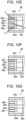
- FIG. 10A illustrates the slit according to embodiments 1 to 4.
- FIGs. 10B to 10G illustrate slits according to variations 1 to 6, respectively.
- the slit 35 in the flexible substrate 30 is not limited to the configuration illustrated in FIG. 10A .
- the width W2 and the length L2 of the slit 35 are not necessarily constant, and can be properly set for adjustment to appropriate impedance.
- the flexible substrate 30 may include, in addition to the slit 35, a slit 35a disposed between the 2a-th signal line 32a and the first ground film conductor 33c, and a slit 35b disposed between the 2b-th signal line 32b and the first ground film conductor 33d.
- the slits 35a and 35b may be oblong along the signal line, and may be aligned with the 2a-th signal line 32a and the 2b-th signal line 32b in the line width direction of the signal line. This configuration additionally provided with the slits 35a and 35b can further suppress an increase in the capacitance components around the joint portion caused by the insulating base 31 of the flexible substrate 30.
- the slit 35, the slits 35a, and the slit 35b may all be equal or different in width and length.
- the slit 35 may be larger in width than at least one of the slits 35a and 35b in an embodiment.
- the flexible substrate 30 may include a slit 35c spaced apart from the second edge E30. This configuration can decrease the capacitance components around the joint portion and can keep the strength of the flexible substrate 30.
- the flexible substrate 30 may include a slit 35d including a plurality of sub-slits s divided from each other in the direction along the signal line.
- This configuration can keep the strength of the flexible substrate 30 and can cause the slit 35d to suppress an increase in the capacitance components of the insulating base 31 around the joint portion.
- the sub-slits s can have any proper shape appropriately selected from a rectangular shape, a square shape, a circular shape, and the like in accordance with design conditions.
- the flexible substrate 30 may include a plurality of slits 35e, 35f, and 35g each of which may include a plurality of sub-slits s divided from each other in the direction along the signal line.
- the slits 35e, 35f, and 35g may be disposed at the same or similar positions of the slits 35, 35a, and 35b illustrated in FIG. 10B . This configuration can keep the strength of the flexible substrate 30 and can further suppress an increase in the capacitance components of the insulating base 31.
- the flexible substrate 30 may include a slit 35h positioned between the 2a-th signal line 32a and the first ground film conductor 33c and spaced apart from the second edge E30.
- the flexible substrate 30 may include a slit 35i positioned between the 2b-th signal line 32b and the first ground film conductor 33d and spaced apart from the second edge E30.
- the flexible substrate 30 may include a slit 35j positioned between the 2a-th signal line 32a and the 2b-th signal line 32b and spaced apart from the second edge E30. This configuration can keep the strength of the flexible substrate 30 and can further suppress an increase in the capacitance components due to the insulating base 31.
- the recess 24 provided as a cutout in the wiring board 20 may include the single recess 24 or a plurality of recesses 24 disposed to face the slits 35b to 35l illustrated in FIGs. 10B to 10G . That is, the recesses 24 may be positioned between the 1a-th signal line 22a and the 1b-th signal line 22b, between the 1a-th signal line 22a and the ground film conductor 23a, and between the 1b-th signal line 22b and the ground film conductor 23b.
- the recesses 24 may be positioned between the 1a-th signal line 22a and the ground film conductor 23a and between the 1b-th signal line 22b and the ground film conductor 23b, and are not necessarily positioned between the 1a-th signal line 22a and the 1b-th signal line 22b.
- the composite wiring board 10 may include the wiring board 20 that includes the recess 24 disposed at any one of the positions described above, and the flexible substrate 30 that includes the slit 35 disposed at any one of the positions described above and is joined to the wiring board 20.
- the recess 24 and the slit 35 may be positioned not to face each other.
- FIGs. 11A to 11C are longitudinal sectional views of cutouts according to variations 7 to 9 disposed in a wiring board, respectively.
- FIGs. 11A, 11B, and 11C each illustrate a section of the wiring board 20 taken at a location provided with the cutout.
- the above embodiment exemplifies the recess 24 as a cutout in the wiring board 20.
- the recess 24 may be replaced with a cutout 24a disposed inside the board.
- the cutout 24a is positioned inside the wiring board 20 to be apart from the board surface and is unopened to the board surface or the end surface of the board.
- the cutout 24a may be shaped identically or similarly to the recess 24 and may be positioned identically or similarly to the recess 24.
- the recess 24 may be replaced with a cutout 24b unopened to the board surface and opened to an end surface S11 of the board.
- the cutout 24b may be shaped identically or similarly to the recess 24 and may be positioned identically or similarly to the recess 24 except for being positioned to reach the first edge E20 in the first joint region R1.
- the cutout 24a or 24b thus provided can suppress a possibility that the bonding material F drops into the cutout. Furthermore, provision of the cutout 24a or 24b can also achieve a suppressed increase in the capacitance components around the joint portion between the first signal line 22 and the second signal line 32.
- the recess 24 may be replaced with a cutout 24c penetrating from the board surface to the opposite surface of the wiring board 20.
- the cutout 24c may be shaped identically or similarly to the recess 24 and may be positioned identically or similarly to the recess 24. Provision of the cutout 24c can achieve a further decrease in the capacitance components of the insulating substrate 21 around the first signal line 22. Accordingly, this can further suppress a decrease in the impedance at the joint portion between the first signal line 22 and the second signal line 32.
- FIG. 12 is a perspective view of an electronic component accommodating package and an electronic device according to an embodiment of the present disclosure.
- the present embodiment provides an electronic component accommodating package 50 including the composite wiring board 10 and the frame 52 integrated with the wiring board 20.
- the frame 52 surrounds an accommodating portion 51 of an electronic component 80.
- the frame 52 may further cover a bottom of the accommodating portion 51 and have an open top. Such an opening may be blocked by joining a lid (not illustrated).
- the first joint region R1 of the wiring board 20 may be positioned outside the frame 52.
- FIG. 12 illustrates the composite wiring board 10 and the electronic component accommodating package 50 that include a set of the first signal line 22 and the second signal line 32.
- the composite wiring board 10 and the electronic component accommodating package 50 may alternatively include a plural sets of first signal lines 22 and second signal lines 32.
- the plural sets of the first signal lines 22 and the second signal line 32 may be aligned in an identical direction or may be positioned at a plurality of locations and directed differently.
- the present embodiment provides an electronic device 100 including electronic component accommodating package 50, and the electronic component 80 accommodated in the accommodating portion 51.
- the first signal line 22 on the wiring board 20 may be positioned from outside the frame 52 to inside the frame 52 and may be electrically connected to the electronic component 80 in the accommodating portion 51 via a bonding member (e.g., a brazing filler metal, a linear conductor, or a belt-shaped conductor).
- the electronic component 80 may be any element such as an element configured to receive a radio-frequency band electrical signal and output light, an element configured to receive an optical signal and output a radio-frequency band electrical signal, or an element configured to receive or output a radio-frequency band electrical signal.
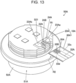
- FIG. 13 is a perspective view of another exemplary electronic component accommodating package according to an embodiment of the present disclosure.
- FIG. 13 is a perspective view of a rear surface of an electronic component accommodating package 50A.
- the electronic component accommodating package 50A has a structure of a TO (transistor outline) package type (e.g., a TO-CAN type), which includes an accommodating portion 51A configured to accommodate an electronic component and disposed on an upper surface (i.e., a lower side in FIG. 13 ) of a wiring board 20A, and a frame 52A joined to an upper end of the wiring board 20A (i.e., a lower end in FIG. 13 ) so as to cover the accommodating portion 51A.
- the electronic component accommodating package 50A includes a composite wiring board 10A including the wiring board 20A and a flexible substrate 30A, and the frame 52A.
- the frame 52A may be a metal member, a ceramic member, or the like.
- the wiring board 20A and the frame 52A may be formed integrally with each other, or may be formed separately and then joined to each other.
- the wiring board 20A and the frame 52A may be both made of a material containing a ceramic and be burned integrally.
- the wiring board 20A includes a lower surface S21 provided with a first signal line 22A and the first joint region R1.
- the second joint region R2 of the flexible substrate 30A is joined to the first joint region R1.
- the first signal line 22A is positioned on the lower surface S21 of the wiring board 20A and from the lower surface S21 to the upper surface.
- the first signal line 22A is joined to a second signal line 32A of the flexible substrate 30A on the lower surface S21, and is electrically connected to the electronic component on the upper surface.
- the first signal line 22A on the wiring board 20A may be a single-ended signal line, and recesses 24A and 24B provided as cutouts may be positioned on respective sides in a line width direction of the first signal line 22A, specifically, between the first signal line 22A and a first ground film conductor 23Aa and between the first signal line 22A and a second ground film conductor 23Ab.
- the first ground film conductor 23Aa and the second ground film conductor 23Ab are positioned on respective sides of the first signal line 22A to interpose the first signal line 22A.
- the second signal line 32A on the flexible substrate 30A is a single-ended signal line, and slits 35A and 35B are positioned on respective sides in a line width direction of the second signal line 32A, specifically, between the second signal line 32A and the first ground film conductors 33c and 33d.
- the electronic component accommodating package 50 or 50A and the electronic device 100 according to the present embodiment include the composite wiring board 10 or 10A according to the embodiment to improve radio-frequency signal transmission characteristics.
- the composite wiring board, an electronic element accommodating package, and the electronic device according to the present disclosure are not limited to the above embodiments, and can be appropriately changed without departing from the purport of the present disclosure.
- the embodiments, the variations, and characterized portions may be combined variously without being limited to the above exemplifications. Furthermore, combination is applicable among the embodiments, among the variations, and among the characterized portions.
- the present disclosure is applicable to a composite wiring board, an electronic component accommodating package, and an electronic device.
Landscapes
- Engineering & Computer Science (AREA)
- Microelectronics & Electronic Packaging (AREA)
- Physics & Mathematics (AREA)
- Electromagnetism (AREA)
- Manufacturing & Machinery (AREA)
- Structure Of Printed Boards (AREA)
Abstract
Description
- The present disclosure relates to a composite wiring board, an electronic component accommodating package, and an electronic device.
-
WO 2019/050046 A discloses a structure for connection between an electronic component accommodating package and a flexible substrate. - According to the present disclosure, a composite wiring board includes a wiring board, and a flexible substrate. The wiring board includes a first joint region. The flexible substrate includes a second joint region overlapped with the first joint region. The wiring board includes a first signal line, and a cutout disposed adjacent to the first signal line. The flexible substrate includes a second signal line to be joined to the first signal line, and a slit disposed adjacent to the second signal line. The cutout is positioned in the first joint region in a plan perspective view. The slit is positioned in the second joint region in a plan perspective view.
- According to the present disclosure, an electronic component accommodating package includes the composite wiring board and a frame positioned on the wiring board.
- According to the present disclosure, an electronic device includes the electronic component accommodating package and an electronic component positioned inside the frame.
-
-
FIG. 1A is a perspective view illustrating a principal part of a composite wiring board according toembodiment 1 of the present disclosure. -
FIG. 1B is a rear-side perspective view illustrating the principal part of the composite wiring board according toembodiment 1 of the present disclosure. -
FIG. 2A is a front-side plan view illustrating a principal part of a flexible substrate. -
FIG. 2B is a rear-side plan view illustrating the principal part of the flexible substrate. -
FIG. 3 is a plan view illustrating a principal part of a wiring board. -
FIG. 4A is a longitudinal sectional view illustrating a joint portion of signal lines and the periphery of the joint portion. -
FIG. 4B is a plan view illustrating the joint portion of the signal lines and the periphery of the joint portion. -
FIG. 5A is a sectional view taken along line A-A inFIG. 4B and explanatorily indicating widths of respective portions. -
FIG. 5B is a sectional view taken along line A-A inFIG. 4B and explanatorily illustrating a superimposed region. -
FIG. 6A is a graph indicating frequency characteristics of composite wiring boards according toembodiment 1 and a comparative example. -
FIG. 6B is a graph indicating impedance characteristics of the composite wiring boards according toembodiment 1 and the comparative example. -
FIG. 7 is a sectional view of a composite wiring board according toembodiment 2. -
FIG. 8 is a sectional view of a composite wiring board according toembodiment 3. -
FIG. 9 is a perspective view of a composite wiring board according toembodiment 4. -
FIG. 10A is a view of a slit according toembodiments 1 to 4. -
FIG. 10B is a view of slits according tovariation 1. -
FIG. 10C is a view of a slit according tovariation 2. -
FIG. 10D is a view of a slit according tovariation 3. -
FIG. 10E is a view of slits according tovariation 4. -
FIG. 10F is a view of slits according tovariation 5. -
FIG. 10G is a view of slits according to variation 6. -
FIG. 11A is a longitudinal sectional view of a cutout according to variation 7 provided in the wiring board. -
FIG. 11B is a longitudinal sectional view of a cutout according to variation 8 provided in the wiring board. -
FIG. 11C is a longitudinal sectional view of a cutout according to variation 9 provided in the wiring board. -
FIG. 12 is a perspective view of an electronic component accommodating package and an electronic device according to an embodiment of the present disclosure. -
FIG. 13 is a perspective view of another exemplary electronic component accommodating package according to an embodiment of the present disclosure. - Embodiments of the present disclosure will be described in detail hereinafter with reference to the drawings.
-
FIG. 1A is a perspective view illustrating a principal part of a composite wiring board according toembodiment 1 of the present disclosure.FIG. 1B is a rear-side perspective view illustrating the principal part of the composite wiring board according toembodiment 1 of the present disclosure.FIGs. 2A and 2B are a front-side plan view and a rear-side plan view each illustrating a principal part of a flexible substrate.FIG. 3 is a plan view illustrating a principal part of a wiring board. -
Embodiment 1 provides acomposite wiring board 10 including awiring board 20 and aflexible substrate 30. - The
wiring board 20 includes an insulatingsubstrate 21, afirst signal line 22 positioned on the insulatingsubstrate 21, and arecess 24 provided as a cutout. - The
recess 24 is disposed adjacent to thefirst signal line 22. Thefirst signal line 22 and therecess 24 adjacent to each other are aligned in a line width direction of thefirst signal line 22, a line direction, or in a direction slanted from the line width direction. When thefirst signal line 22 and therecess 24 are disposed adjacent to each other, a center line in the line direction of thefirst signal line 22 and a center line in a longitudinal direction of therecess 24 may be parallel or nonparallel to each other. Therecess 24 may be positioned around thefirst signal line 22. Being positioned around thefirst signal line 22 can mean being positioned close enough to influence transmission characteristics of thefirst signal line 22, and can mean that distance from thefirst signal line 22 is twice or less a line width of thefirst signal line 22. - The
wiring board 20 may further include aground conductor 23 positioned on the insulatingsubstrate 21. - The insulating
substrate 21 may be made of a ceramic or a resin.FIGs. 1 to 5 exemplarily illustrate thewiring board 20 integrated with aframe 52. Alternatively, theframe 52 may be removed. The insulatingsubstrate 21 may have a plate shape without theframe 52. Theframe 52 may be formed integrally with thewiring board 20, or may be formed separately and joined to thewiring board 20. The insulatingsubstrate 21 and theframe 52 may interpose a different member. - The
first signal line 22 is a signal line configured to transmit a radio-frequency signal. Thefirst signal line 22 may be single-ended as a single signal line, or may include two signal lines, namely, a 1a-th signal line 22a and a 1b-th signal line 22b. The 1a-th signal line 22a and the 1b-th signal line 22b may be parallel to each other. The 1a-th signal line 22a and the 1b-th signal line 22b may be signal lines each configured to transmit a differential signal. - The first signal line 22 (i.e., the 1a-
th signal line 22a and the 1b-th signal line 22b) may be positioned on an upper surface of the insulatingsubstrate 21. Part of thefirst signal line 22 may be positioned on the upper surface of the insulatingsubstrate 21 whereas the remaining part may be positioned inside the insulatingsubstrate 21 or on a rear surface of the insulatingsubstrate 21. When theframe 52 is provided, part of thefirst signal line 22 may be positioned inside the frame 52 (e.g., between theframe 52 and the insulating substrate 21). - The
recess 24 may be positioned between the 1a-th signal line 22a and the 1b-th signal line 22b. Therecess 24 may be shaped to be oblong along the signal line. Therecess 24 may have an oval shape or a rectangular shape in a plan perspective view. Plan perspective view means perspectively viewing in a direction vertical to a board surface of thewiring board 20 provided with thefirst signal line 22. Therecess 24 may be opened to the board surface. Therecess 24 may have a tapered shape, an inversely tapered shape, or a stepped shape in a sectional view. Therecess 24 in the tapered shape includes an open end wider than a bottom end, whereas therecess 24 in the inversely tapered shape includes the bottom end wider than the open end. Therecess 24 may be distant from or in contact with the 1a-th signal line 22a and the 1b-th signal line 22b. - The
ground conductor 23 may includeground film conductors FIG. 3 ) positioned on respective sides of the first signal line 22 (i.e., the 1a-th signal line 22a and the 1b-th signal line 22b), aground film conductor 23c (seeFIG. 3 ) positioned on a bottom surface of therecess 24, aground film conductor 23d (seeFIG. 1A ) expanding in a layer below thefirst signal line 22, aground film conductor 23e (seeFIG. 1A ) expanding in a layer above thefirst signal line 22 inside theframe 52 when theframe 52 is provided, a ground via conductor 23v1 (seeFIG. 1A ) configured to provide conductivity between theground film conductors ground film conductor 23d positioned in the lower layer, and a ground via conductor 23v2 (seeFIG. 1A ) configured to provide conductivity between theground film conductors ground film conductor 23e positioned in the upper layer. Theground conductor 23 may further include aground line 23h (seeFIG. 3 ) positioned between the 1a-th signal line 22a and the 1b-th signal line 22b, and a ground via conductor (not illustrated) configured to provide conductivity between theground line 23h and theground film conductor - The
ground film conductors th signal line 22a and the 1b-th signal line 22b). - The
ground line 23h may be positioned between the 1a-th signal line 22a and the 1b-th signal line 22b outside a region provided with therecess 24. - As illustrated in
FIGs. 1A, 1B , and3 , thewiring board 20 includes a first joint region R1 overlapped with theflexible substrate 30. Thewiring board 20 may include a first edge E20 disposed at one end of the board surface and crossing an extension of thefirst signal line 22, and the first joint region R1 may include the first edge E20. When theframe 52 is provided, the first joint region R1 may expand to a foot of theframe 52. That is, theframe 52 and an edge of theflexible substrate 30 may be in contact with each other. - As illustrated in
FIG. 3 , the first joint region R1 may include part of the first signal line 22 (i.e., the 1a-th signal line 22a and the 1b-th signal line 22b), therecess 24, part of theground film conductors ground film conductor 23c, which are mentioned above. - Part including line ends of the 1a-
th signal line 22a and the 1b-th signal line 22b may be positioned in the first joint region R1. An end of the 1a-th signal line 22a and an end of the 1b-th signal line 22b may be spaced apart from the first edge E20. The 1a-th signal line 22a and the 1b-th signal line 22b may be exposed onto the first joint region R1. - The
recess 24 may entirely be positioned in the first joint region R1. - The
ground film conductors ground film conductors flexible substrate 30 in a plan perspective view. In the first joint region R1, an interval between the twoground film conductors ground film conductors - The
ground film conductor 23c may be positioned on the bottom surface of therecess 24. The bottom surface of therecess 24 and theground film conductor 23c may be covered from above with an insulatingfilm 25. The insulatingfilm 25 may be alumina coating. Thefirst signal line 22 or therecess 24 may be in contact with the first edge E20. Therecess 24 may be opened to an end surface of thewiring board 20. Therecess 24 may be a hole penetrating from an upper surface to a lower surface of thewiring board 20. - As illustrated in
FIGs. 2A and 2B , theflexible substrate 30 may include an insulatingbase 31 having flexibility and a sheet shape. The insulatingbase 31 includes a first surface S1 and a second surface S2 positioned opposite to the first surface S1. - The
flexible substrate 30 includes asecond signal line 32 positioned on the first surface S1. Thesecond signal line 32 may partially be joined to thefirst signal line 22 on thewiring board 20, and may be equal in number of lines to thefirst signal line 22. Thesecond signal line 32 may therefore include two signal lines, namely, a 2a-th signal line 32a and a 2b-th signal line 32b. The 2a-th signal line 32a and the 2b-th signal line 32b may be parallel to each other. The 2a-th signal line 32a and the 2b-th signal line 32b may be signal lines each configured to transmit a differential signal. Thesecond signal line 32 may includeelectrode pads electrode pads second signal line 32. - The
flexible substrate 30 further includes aslit 35 disposed adjacent to thesecond signal line 32. Thesecond signal line 32 and theslit 35 adjacent to each other are aligned in a line width direction of thesecond signal line 32, a line direction, or in a direction slanted from the line width direction. When thesecond signal line 32 and theslit 35 are disposed adjacent to each other, a center line in the line direction of thesecond signal line 32 and a center line in a longitudinal direction of theslit 35 are not necessarily parallel to each other. Theslit 35 may be positioned around thesecond signal line 32. Being positioned around thesecond signal line 32 can mean being positioned close enough to influence transmission characteristics of thesecond signal line 32, and can mean that distance from thesecond signal line 32 is twice or less the line width of thesecond signal line 32. Theslit 35 may be positioned from the first surface S1 to the second surface S2. Theslit 35 may be hollow. Theslit 35 may have a rectangular shape, a circular shape, an oblong shape, an elliptical shape, or the like. Theslit 35 has a width that may be increased as being away from the second edge E30 or may inversely be decreased as being away from the second edge E30. Theslit 35 may have a tapered shape, an inversely tapered shape, or a stepped shape in a sectional view. The tapered shape has a slanted side surface with a size at a level of the second surface S2 being larger than a size at a level of the first surface S1. The inversely tapered shape has a slanted side surface with a size at the level of the second surface S2 being smaller than a size at the level of the first surface S1. Furthermore, theslit 35 may be distant from or in contact with thesecond signal line 32. - The
flexible substrate 30 may further include a film conductor positioned on the first surface S1 and the second surface S2, and a via conductor positioned from the first surface S1 to the second surface S2, which are to be described later. - The film conductor may include
electrode film conductors ground film conductor 33e positioned on the second surface S2, and firstground film conductors second signal line 32 on the first surface S1. Theelectrode film conductors electrode pads second signal line 32. The secondground film conductor 33e may expand around theelectrode film conductors electrode film conductors - The via conductor may include electrode via
conductors 34a to 34d connecting theelectrode pads electrode film conductors ground film conductors ground film conductor 33e. The plurality of ground via conductors may interpose the 2a-th signal line 32a and the 2b-th signal line 32b and be aligned along the signal lines. - As illustrated in
FIGs. 2A and 2B , theflexible substrate 30 includes a second joint region R2 overlapped with the first joint region R1 of thewiring board 20. Theflexible substrate 30 may include the second edge E30 disposed at one end and crossing an extension of thesecond signal line 32, and the second joint region R2 may include the second edge E30. - The second joint region R2 may be provided with the
electrode pads second signal line 32, part of the firstground film conductors slit 35. - An opposite surface of the second joint region R2 may be provided with the
electrode film conductors ground film conductor 33e, and theslit 35. - In the second joint region R2, the
electrode pads ground film conductors electrode film conductors ground film conductor 33e may be spaced apart from the second edge E30. Theslit 35 may be positioned to reach the second edge E30. - As illustrated in
FIG. 2A , theelectrode film conductors conductors 34a to 34d and that may be wider than the remaining portions. That is, theelectrode film conductors - The second
ground film conductor 33e may include uneven portions N3 and N4 including portions projecting in the line width direction and portions depressed in the line width direction which are alternately aligned in portions facing theelectrode film conductors electrode film conductors ground film conductor 33e may be disposed staggeredly. That is, the concave portions in the uneven portions N1 and N2 and the convex portions in the uneven portions N3 and N4 may be aligned in the line width direction, and the convex portions in the uneven portions N1 and N2 and the concave portions in the uneven portions N3 and N4 may be aligned in the line width direction. -
FIGs. 4A and 4B are a longitudinal sectional view and a plan view each illustrating a joint portion of the signal lines and the periphery of the joint portion.FIGs. 5A and 5B are sectional views taken along line A-A inFIG. 4B .FIGs. 5A and 5B illustrate an identical location. - The first joint region R1 of the
wiring board 20 and the second joint region R2 of theflexible substrate 30 are overlapped with each other. Part of the first joint region R1 and part of the second joint region R2 may be joined to each other via a bonding material F such as a brazing filler metal having electroconductivity (seeFIGs. 4A ,5A, and 5B ). Specifically, thefirst signal line 22 in the first joint region R1 and theelectrode pads second signal line 32 may be joined), and theground film conductors ground film conductors FIG. 2B ) in the second joint region R2 may be joined to each other via the bonding material F. - For Joining, heat is applied to an opposite side of the second joint region R2 of the
flexible substrate 30 in the state where the first joint region R1 and the second joint region R2 are overlapped with each other, to transfer heat to the bonding material F at each site via the conductors on theflexible substrate 30 and melt the bonding material F. The bonding material F is then cooled to be solidified, and the first joint region R1 and the second joint region R2 are joined to each other. - As described above, the
wiring board 20 includes thefirst signal line 22, and therecess 24 provided as a cutout and disposed adjacent to thefirst signal line 22. Theflexible substrate 30 includes thesecond signal line 32, and theslit 35 disposed adjacent to thesecond signal line 32. Therecess 24 is positioned in the first joint region R1 whereas theslit 35 is positioned in the second joint region R2 in a plan perspective view. This configuration can suppress an increase in the capacitance components (e.g., electrostatic capacitance components) around the joint portion between thefirst signal line 22 and thesecond signal line 32. That is, the joint portion is provided with thewiring board 20 and the insulatingbase 31 each having a high relative dielectric constant. This is likely to increase capacitance components around thefirst signal line 22 and thesecond signal line 32 and decrease characteristic impedance. However, theslit 35 thus provided can decrease a relative dielectric constant around thesecond signal line 32 on the insulatingbase 31. The joint portion can therefore have a suppressed increase in the capacitance components of thesecond signal line 32. Furthermore, therecess 24 thus provided can decrease a relative dielectric constant around thefirst signal line 22 on the insulatingsubstrate 21. The joint portion can therefore have a suppressed increase in the capacitance components of thefirst signal line 22. Accordingly, the joint portion between thefirst signal line 22 and thesecond signal line 32 can have a suppressed possibility of an increase in capacitance components and improved characteristic impedance matching. Thecomposite wiring board 10 can therefore be improved in radio-frequency signal transmission characteristics. - As described above, the
slit 35 may be positioned to reach the second edge E30 of theflexible substrate 30. This configuration can further suppress an increase in the capacitance components around thesecond signal line 32. The joint portion between thefirst signal line 22 and thesecond signal line 32 can therefore have an efficiently suppressed increase in capacitance components. Accordingly, the joint portion can have more improved characteristic impedance matching and more improved radio-frequency signal transmission characteristics. - The
second signal line 32 may include the 2a-th signal line 32a and the 2b-th signal line 32b disposed parallel to each other. As described above, and theslit 35 may be positioned between the 2a-th signal line 32a and the 2b-th signal line 32b. In this configuration, due to symmetry between thefirst signal line 22 and thesecond signal line 32, thefirst signal line 22 on thewiring board 20 includes the 1a-th signal line 22a and the 1b-th signal line 22b. Provision of theslit 35 as described above can achieve a suppress increase in the capacitance components between the 2a-th signal line 32a and the 2b-th signal line 32b. The joint portion between thefirst signal line 22 and thesecond signal line 32 can therefore have an efficiently suppressed increase in capacitance components and can be improved in radio-frequency signal transmission characteristics. - The
recess 24 provided as a cutout and theslit 35 may be at least partially overlapped with each other in a plan perspective view (seeFIG. 4B ). This configuration can decrease capacitance components of the insulatingsubstrate 21 and capacitance components of the insulatingbase 31 at symmetrical locations on the insulatingsubstrate 21 and the insulatingbase 31. This can therefore achieve a decreased difference in characteristic impedance between the joint portion of thefirst signal line 22 and thesecond signal line 32 and locations in front of and behind the joint portion. This can therefore improve radio-frequency signal transmission characteristics. Furthermore, therecess 24 and theslit 35 are preferably overlapped with each other by 50% or more in area ratio in a plan perspective view (that is, in a plan perspective view, 50% or more of the total area of therecess 24 is overlapped with theslit slit 35 is overlapped with the recess 24). Overlapping by 50% or more in area ratio can achieve a decrease in the capacitance components of the insulatingsubstrate 21 and a decrease in the capacitance components of the insulatingbase 31. - The
slit 35 has a size L2 (seeFIG. 2B ) in the direction along the signal line, and the size L2 may be larger than a size L1 (seeFIG. 3 ) of therecess 24 in the direction. This configuration can stably secure an overlapping length between theslit 35 and therecess 24 even with any joined position error in the direction along the signal line. The joint portion can therefore have a stably suppressed increase in capacitance components and can stably be improved in radio-frequency signal transmission characteristics. - The
recess 24 has a width W1 (specifically a width in the line width direction of the signal line, seeFIGs. 3 and5A ) which may be larger than a width W2 of the slit 35 (specifically a width in the line width direction of the signal line, seeFIGs. 2B and5A ). This configuration can suppress overlapping between part of thefirst signal line 22 and theslit 35 even with any joined position error in the width direction of the signal line. The first j oint region R1 can thus stably achieve a structure in which theflexible substrate 30 overlaps on thefirst signal line 22. This structure can suppress large individual differences in characteristic impedance. This leads to stable radio-frequency signal transmission characteristics. - The
recess 24 has a thickness D1 (i.e., a length perpendicular to the board surface) which may be larger than a thickness D2 of the slit 35 (seeFIG. 5A ). In a case where influence on impedance matching of thecomposite wiring board 10 is largely caused by the capacitance components of thefirst signal line 22 and the thickness D1 is larger than the thickness D2, thewiring board 20 can have a further suppressed increase in capacitance components. Thecomposite wiring board 10 can therefore achieve stable radio-frequency signal transmission characteristics. The thickness D1 of therecess 24 may exemplarily be defined as the minimum distance from the board surface to the bottom surface of therecess 24. - In the direction along the signal line, the size L2 (see
FIG. 2B ) of theslit 35 may be larger than a size L3 (seeFIG. 4B ) of a superimposed region M. The superimposed region M corresponds to a region where thefirst signal line 22 and thesecond signal line 32 are joined to each other (i.e., a region provided with the bonding material F) (seeFIGs. 4B and5B ).FIG. 4B illustrates the superimposed region M by hatching. In this configuration, the joint portion is likely to have a further decrease in the capacitance components around thesecond signal line 32. This can therefore more efficiently decrease the capacitance components and can improve radio-frequency signal transmission characteristics. - In the superimposed region M, the 1a-
th signal line 22a has a line width W3 that may be smaller than a line width W4 of the 2a-th signal line 32a (specifically the width W4 of theelectrode pad 32c) (seeFIG. 5A ). This configuration can suppress extrusion of the 1a-th signal line 22a from the 2a-th signal line 32a (specifically theelectrode pad 32c) in a plan perspective view even with any joined position error in the width direction of the signal line. The superimposed region M can thus stably achieve a structure in which the 2a-th signal line 32a (specifically theelectrode pad 32c) overlaps on the 1a-th signal line 22a. This structure can suppress large individual differences in characteristic impedance. This leads to stable radio-frequency signal transmission characteristics. The line width W3 of the 1a-th signal line 22a may have the maximum size of the line width W3 of the 1a-th signal line 22a. - In the same or a similar manner, in the superimposed region M, the line width W3 of the 1b-
th signal line 22b may be smaller than the line width W4 of the 2b-th signal line 32b (specifically the width W4 of theelectrode pad 32d) (seeFIG. 5A ). This configuration can suppress extrusion of the 1b-th signal line 22b from the 2b-th signal line 32b (specifically theelectrode pad 32d) in a plan perspective view even with any joined position error in the width direction of the signal line. The superimposed region M can thus stably achieve a structure in which the 2b-th signal line 32b (specifically theelectrode pad 32d) overlaps on the 1b-th signal line 22b. This structure can suppress large individual differences in characteristic impedance. This leads to stable radio-frequency signal transmission characteristics. - The electrode film conductors (corresponding to first film conductors) 33a and 33b may be smaller in area than the superimposed region M (see
FIG. 4B ). This configuration can also allow heat to be conducted from the second surface S2 to theelectrode pads electrode film conductors electrode film conductors electrode film conductors second signal line 32. Therefore, the joint portion between thefirst signal line 22 and thesecond signal line 32 can have improved characteristic impedance matching and improved radio-frequency signal transmission characteristics. - The
slit 35 includes a first slit end portion t35 (seeFIG. 4B ) positioned far from the second edge E30 of theflexible substrate 30. In a plan perspective view, the first slit end portion t35 may be spaced apart from the first edge E20 of the first joint region R1 and positioned on the first joint region R1. This configuration can suppress curving at the first slit end portion t35, so that theslit 35 is less likely to receive stress. Theflexible substrate 30 can therefore have a suppressed possibility of damage at the first slit end portion t35. - The
recess 24 may be opened to the board surface of thewiring board 20. Thewiring board 20 may include the insulating film 25 (seeFIG. 3 ) positioned on the bottom surface of therecess 24. This configuration can suppress a possibility of a short circuit between theground film conductor 23c in therecess 24 and each of thefirst signal line 22 and thesecond signal line 32 even in a case where the bonding material F joining thefirst signal line 22 and thesecond signal line 32 drops into therecess 24. Thecomposite wiring board 10 can therefore be improved in radio-frequency signal transmission characteristics. - The
second signal line 32 may be distant from theslit 35 with a clearance Q (seeFIG. 2B ) provided therebetween in a plan perspective view. This configuration is less likely to cause the bonding material F joining thefirst signal line 22 and thesecond signal line 32 to expand to an inner circumferential surface of theslit 35 and influence characteristic impedance at the joint portion. Thecomposite wiring board 10 can therefore be improved in radio-frequency signal transmission characteristics. -
FIG. 6A is a graph indicating frequency characteristics of composite wiring boards according toembodiment 1 and a comparative example.FIG. 6B is a graph indicating impedance characteristics of the composite wiring boards according toembodiment 1 and the comparative example. The graphs indicate simulation results of thecomposite wiring board 10 according to the embodiment and the composite wiring board according to the comparative example. Frequency characteristics include an insertion loss and a return loss, and impedance characteristics are indicated in accordance with TDR (time domain reflectometry). Simulation adopts thecomposite wiring board 10 according to the embodiment including the constituent elements described above and being configured as illustrated inFIGs. 1 to 6 . The composite wiring board according to the comparative example has a configuration obtained by removing theslit 35 from the configuration according to the embodiment. -
FIG. 6A indicates that the return loss decreases in the range from 3 GHz to 40 GHz as well as that deterioration of insertion loss characteristics is suppressed in a high band when therecess 24 is positioned in the first joint region R1 and theslit 35 is positioned in the second joint region R2. -
FIG. 6B indicates that a difference in characteristic impedance is decreased between a location around the joint portion and the location in front of the joint portion as well as between the location around the joint portion and the location behind the joint portion to improve characteristic impedance matching when therecess 24 is positioned in the first joint region R1 and theslit 35 is positioned in the second joint region R2. TDR includes a time domain from 20 ps to 40 ps indicating impedance around the joint portion. - As described above, the
composite wiring board 10 according to the above embodiment can have improved characteristic impedance matching at the joint portion between thewiring board 20 and theflexible substrate 30, and can achieve improved radio-frequency signal transmission characteristics. -
FIG. 7 is a sectional view of a composite wiring board according toembodiment 2.FIG. 7 illustrates a section positioned identically to a section illustrated inFIG. 5A .Embodiment 2 provides acomposite wiring board 10 configured in the same or a similar manner to the composite wiring board according toembodiment 1 except for part of elements. Description is hereinafter made to such elements different from the elements according toembodiment 1. - In the superimposed region M (see
FIGs. 4B and5B ), a center CL1 in the line width direction of the 1a-th signal line 22a may be displaced from a center CL2 in the line width direction of the 2a-th signal line 32a (specifically theelectrode pad 32c) to one side in the line width direction (seeFIG. 7 ). The center CL1 of the 1a-th signal line 22a may be displaced from the center CL2 of the 2a-th signal line 32a (specifically theelectrode pad 32c) to approach therecess 24. That is, distance between therecess 24 and the center CL1 in the line width direction of the 1a-th signal line 22a may be shorter than distance between therecess 24 and the center CL2 in the line width direction of the 2a-th signal line 32a. - In the same or a similar manner, in the superimposed region M (see
FIGs. 4B and5B ), a center CL3 in the line width direction of the 1b-th signal line 22b may be displaced from a center CL4 in the line width direction of the 2b-th signal line 32b (specifically theelectrode pad 32d) to one side in the line width direction (seeFIG. 7 ). The center CL3 of the 1b-th signal line 22b may be displaced from the center CL4 of the 2b-th signal line 32b (specifically theelectrode pad 32c) to approach therecess 24. That is, distance between therecess 24 and the center CL3 in the line width direction of the 1b-th signal line 22b may be shorter than distance between therecess 24 and the center CL4 in the line width direction of the 2b-th signal line 32b. - The above positional relationship between the centers CL3 and CL4 can increase an area where the
recess 24 and theslit 35 are overlapped with each other. Thecomposite wiring board 10 can therefore be further improved in radio-frequency signal transmission characteristics. -
FIG. 8 is a sectional view of a composite wiring board according toembodiment 3.FIG. 8 illustrates a section positioned identically to the section illustrated inFIG. 5A .Embodiment 3 provides acomposite wiring board 10 configured in the same or a similar manner to the composite wiring board according toembodiment 1 except for part of elements. Description is hereinafter made to such elements different from the elements according toembodiment 1. - The
recess 24 may include an upper layer portion 241 and a lower layer portion 242, and the upper layer portion 241 and the lower layer portion 242 may be disposed vertically continuously. The upper layer portion 241 has a width W1 (specifically a width in the line width direction of the signal line) which may be different from a width W1a (specifically a width in the line width direction of the signal line) of the lower layer portion 242. For example, the width W1a > the width W1 may be established. That is, the width W1a may be larger than the width W1. - Furthermore, the width W1 of the upper layer portion 241 < an interval W5 between the 1a-
th signal line 22a and the 1b-th signal line 22b < the width W1a of the lower layer portion 242 may be established. That is, the width W1 of the upper layer portion 241 may be smaller than the interval W5, and the width W1a of the lower layer portion 242 may be larger than the interval W5. The interval W5 is distance between the 1a-th signal line 22a and the 1b-th signal line 22b. - Furthermore, the width W1 of the upper layer portion 241 may be larger than the width W2 of the
slit 35, and the width W2 of the lower layer portion 242 may be larger than the width W2 of theslit 35. - A center in a width direction of the upper layer portion 241 may be overlapped with a center in a width direction of the lower layer portion 242 in a plan perspective view.
- The insulating
substrate 21 may have a stacked structure including a plurality of stacked dielectric layers. In this case, the upper layer portion 241 of therecess 24 may be positioned in an n-th dielectric layer of the insulatingsubstrate 21, and the lower layer portion 242 of therecess 24 may be positioned in an (n+1)-th dielectric layer of the insulatingsubstrate 21. - In the above configuration, the width W1 of the upper layer portion 241 is limited by the 1a-
th signal line 22a and the 1b-th signal line 22b, whereas the width W1a of the lower layer portion 242 can be increased without such limitation. The large width W1a of the lower layer portion 242 can further decrease the relative dielectric constant around thefirst signal line 22 on the insulatingsubstrate 21. The joint portion can thus have a further suppressed increase in the capacitance components of thefirst signal line 22. Accordingly, the joint portion between thefirst signal line 22 and thesecond signal line 32 can have a suppressed increase in capacitance components and improved characteristic impedance matching. Thecomposite wiring board 10 can therefore be improved in radio-frequency signal transmission characteristics. -
FIG. 9 is a perspective view of a composite wiring board according toembodiment 4.Embodiment 4 provides acomposite wiring board 10 configured in the same or a similar manner to the composite wiring board according toembodiment 1 except for part of elements. Description is hereinafter made to such elements different from the elements according toembodiment 1. - As illustrated in
FIG. 9 , theflexible substrate 30 may include aprotective film 37a covering to protect part of the second signal line 32 (corresponding to a conductor layer) and part of the firstground film conductors flexible substrate 30 may further include aprotective film 37b covering to protect part of the secondground film conductor 33e (corresponding to a conductor layer) on the second surface S2. Each of theprotective films - The
protective film 37a on the first surface S1 may be positioned outside the first joint region R1. Theprotective film 37a is not necessarily overlapped with theslit 35 in a plan perspective view. - The
protective film 37b on the second surface S2 may be positioned in a region excluding theelectrode film conductors second signal line 32 and a range aligned with theelectrode film conductors ground film conductor 33e (specifically a range aligned in the line width direction of the signal line). Theprotective film 37b is not necessarily overlapped with theslit 35. - In the
composite wiring board 10 according toembodiment 4, theprotective films flexible substrate 30, and can suppress a short circuit and the like of the conductors. Theprotective films flexible substrate 30. Moreover, theslit 35 is not overlapped with theprotective films protective films slit 35 of improving specific impedance matching. -
FIG. 10A illustrates the slit according toembodiments 1 to 4.FIGs. 10B to 10G illustrate slits according tovariations 1 to 6, respectively. Theslit 35 in theflexible substrate 30 is not limited to the configuration illustrated inFIG. 10A . The width W2 and the length L2 of theslit 35 are not necessarily constant, and can be properly set for adjustment to appropriate impedance. - As illustrated in
FIG. 10B , theflexible substrate 30 may include, in addition to theslit 35, aslit 35a disposed between the 2a-th signal line 32a and the firstground film conductor 33c, and aslit 35b disposed between the 2b-th signal line 32b and the firstground film conductor 33d. Theslits th signal line 32a and the 2b-th signal line 32b in the line width direction of the signal line. This configuration additionally provided with theslits base 31 of theflexible substrate 30. Theslit 35, theslits 35a, and theslit 35b may all be equal or different in width and length. For example, theslit 35 may be larger in width than at least one of theslits - As illustrated in
FIG. 10C , theflexible substrate 30 may include aslit 35c spaced apart from the second edge E30. This configuration can decrease the capacitance components around the joint portion and can keep the strength of theflexible substrate 30. - As illustrated in
FIG. 10D , theflexible substrate 30 may include aslit 35d including a plurality of sub-slits s divided from each other in the direction along the signal line. This configuration can keep the strength of theflexible substrate 30 and can cause theslit 35d to suppress an increase in the capacitance components of the insulatingbase 31 around the joint portion. The sub-slits s can have any proper shape appropriately selected from a rectangular shape, a square shape, a circular shape, and the like in accordance with design conditions. - As illustrated in
FIG. 10E , theflexible substrate 30 may include a plurality ofslits 35e, 35f, and 35g each of which may include a plurality of sub-slits s divided from each other in the direction along the signal line. Theslits 35e, 35f, and 35g may be disposed at the same or similar positions of theslits FIG. 10B . This configuration can keep the strength of theflexible substrate 30 and can further suppress an increase in the capacitance components of the insulatingbase 31. - As illustrated in
FIG. 10F , theflexible substrate 30 may include aslit 35h positioned between the 2a-th signal line 32a and the firstground film conductor 33c and spaced apart from the second edge E30. In the same or a similar manner, theflexible substrate 30 may include aslit 35i positioned between the 2b-th signal line 32b and the firstground film conductor 33d and spaced apart from the second edge E30. In the same or a similar manner, theflexible substrate 30 may include aslit 35j positioned between the 2a-th signal line 32a and the 2b-th signal line 32b and spaced apart from the second edge E30. This configuration can keep the strength of theflexible substrate 30 and can further suppress an increase in the capacitance components due to the insulatingbase 31. - As illustrated in
FIG. 10G , theflexible substrate 30 may include twoslits 35k and 35l positioned between the 2a-th signal line 32a and the firstground film conductor 33c and between the 2b-th signal line 32b and the firstground film conductor 33d, and may include no slit between the 2a-th signal line 32a and the 2b-th signal line 32b. This configuration can cause theslits base 31 around the joint portion even when the 2a-th signal line 32a and the 2b-th signal line 32b interpose a narrow interval. - The
recess 24 provided as a cutout in thewiring board 20 may include thesingle recess 24 or a plurality ofrecesses 24 disposed to face theslits 35b to 35l illustrated inFIGs. 10B to 10G . That is, therecesses 24 may be positioned between the 1a-th signal line 22a and the 1b-th signal line 22b, between the 1a-th signal line 22a and theground film conductor 23a, and between the 1b-th signal line 22b and theground film conductor 23b. Alternatively, therecesses 24 may be positioned between the 1a-th signal line 22a and theground film conductor 23a and between the 1b-th signal line 22b and theground film conductor 23b, and are not necessarily positioned between the 1a-th signal line 22a and the 1b-th signal line 22b. - Furthermore, the
composite wiring board 10 according to the present embodiment may include thewiring board 20 that includes therecess 24 disposed at any one of the positions described above, and theflexible substrate 30 that includes theslit 35 disposed at any one of the positions described above and is joined to thewiring board 20. Therecess 24 and theslit 35 may be positioned not to face each other. -
FIGs. 11A to 11C are longitudinal sectional views of cutouts according to variations 7 to 9 disposed in a wiring board, respectively.FIGs. 11A, 11B, and 11C each illustrate a section of thewiring board 20 taken at a location provided with the cutout. The above embodiment exemplifies therecess 24 as a cutout in thewiring board 20. As illustrated inFIG. 11A , therecess 24 may be replaced with acutout 24a disposed inside the board. Thecutout 24a is positioned inside thewiring board 20 to be apart from the board surface and is unopened to the board surface or the end surface of the board. In a plan perspective view, thecutout 24a may be shaped identically or similarly to therecess 24 and may be positioned identically or similarly to therecess 24. - As illustrated in
FIG. 11B , therecess 24 may be replaced with acutout 24b unopened to the board surface and opened to an end surface S11 of the board. In a plan perspective view, thecutout 24b may be shaped identically or similarly to therecess 24 and may be positioned identically or similarly to therecess 24 except for being positioned to reach the first edge E20 in the first joint region R1. - The
cutout cutout first signal line 22 and thesecond signal line 32. - As illustrated in
FIG. 11C , therecess 24 may be replaced with acutout 24c penetrating from the board surface to the opposite surface of thewiring board 20. In a plan perspective view, thecutout 24c may be shaped identically or similarly to therecess 24 and may be positioned identically or similarly to therecess 24. Provision of thecutout 24c can achieve a further decrease in the capacitance components of the insulatingsubstrate 21 around thefirst signal line 22. Accordingly, this can further suppress a decrease in the impedance at the joint portion between thefirst signal line 22 and thesecond signal line 32. -
FIG. 12 is a perspective view of an electronic component accommodating package and an electronic device according to an embodiment of the present disclosure. - The present embodiment provides an electronic component
accommodating package 50 including thecomposite wiring board 10 and theframe 52 integrated with thewiring board 20. Theframe 52 surrounds anaccommodating portion 51 of anelectronic component 80. Theframe 52 may further cover a bottom of theaccommodating portion 51 and have an open top. Such an opening may be blocked by joining a lid (not illustrated). - The first joint region R1 of the
wiring board 20 may be positioned outside theframe 52. -
FIG. 12 illustrates thecomposite wiring board 10 and the electronic componentaccommodating package 50 that include a set of thefirst signal line 22 and thesecond signal line 32. Thecomposite wiring board 10 and the electronic componentaccommodating package 50 may alternatively include a plural sets offirst signal lines 22 and second signal lines 32. The plural sets of thefirst signal lines 22 and thesecond signal line 32 may be aligned in an identical direction or may be positioned at a plurality of locations and directed differently. - The present embodiment provides an
electronic device 100 including electronic componentaccommodating package 50, and theelectronic component 80 accommodated in theaccommodating portion 51. Thefirst signal line 22 on thewiring board 20 may be positioned from outside theframe 52 to inside theframe 52 and may be electrically connected to theelectronic component 80 in theaccommodating portion 51 via a bonding member (e.g., a brazing filler metal, a linear conductor, or a belt-shaped conductor). Theelectronic component 80 may be any element such as an element configured to receive a radio-frequency band electrical signal and output light, an element configured to receive an optical signal and output a radio-frequency band electrical signal, or an element configured to receive or output a radio-frequency band electrical signal. -
FIG. 13 is a perspective view of another exemplary electronic component accommodating package according to an embodiment of the present disclosure.FIG. 13 is a perspective view of a rear surface of an electronic componentaccommodating package 50A. - The electronic component
accommodating package 50A has a structure of a TO (transistor outline) package type (e.g., a TO-CAN type), which includes anaccommodating portion 51A configured to accommodate an electronic component and disposed on an upper surface (i.e., a lower side inFIG. 13 ) of awiring board 20A, and aframe 52A joined to an upper end of thewiring board 20A (i.e., a lower end inFIG. 13 ) so as to cover theaccommodating portion 51A. That is, the electronic componentaccommodating package 50A includes acomposite wiring board 10A including thewiring board 20A and aflexible substrate 30A, and theframe 52A. In this case, theframe 52A may be a metal member, a ceramic member, or the like. Thewiring board 20A and theframe 52A may be formed integrally with each other, or may be formed separately and then joined to each other. Thewiring board 20A and theframe 52A may be both made of a material containing a ceramic and be burned integrally. - The
wiring board 20A includes a lower surface S21 provided with afirst signal line 22A and the first joint region R1. The second joint region R2 of theflexible substrate 30A is joined to the first joint region R1. - The
first signal line 22A is positioned on the lower surface S21 of thewiring board 20A and from the lower surface S21 to the upper surface. Thefirst signal line 22A is joined to asecond signal line 32A of theflexible substrate 30A on the lower surface S21, and is electrically connected to the electronic component on the upper surface. - As exemplarily illustrated in
FIG. 13 , thefirst signal line 22A on thewiring board 20A may be a single-ended signal line, and recesses 24A and 24B provided as cutouts may be positioned on respective sides in a line width direction of thefirst signal line 22A, specifically, between thefirst signal line 22A and a first ground film conductor 23Aa and between thefirst signal line 22A and a second ground film conductor 23Ab. The first ground film conductor 23Aa and the second ground film conductor 23Ab are positioned on respective sides of thefirst signal line 22A to interpose thefirst signal line 22A. - The
second signal line 32A on theflexible substrate 30A is a single-ended signal line, and slits 35A and 35B are positioned on respective sides in a line width direction of thesecond signal line 32A, specifically, between thesecond signal line 32A and the firstground film conductors - The electronic component
accommodating package electronic device 100 according to the present embodiment include thecomposite wiring board - The embodiments of the present disclosure have been described above. However, the composite wiring board, an electronic element accommodating package, and the electronic device according to the present disclosure are not limited to the above embodiments, and can be appropriately changed without departing from the purport of the present disclosure. The embodiments, the variations, and characterized portions may be combined variously without being limited to the above exemplifications. Furthermore, combination is applicable among the embodiments, among the variations, and among the characterized portions.
- The present disclosure is applicable to a composite wiring board, an electronic component accommodating package, and an electronic device.
-
- 10 composite wiring board
- 20, 20A wiring board
- 21 insulating substrate
- 22, 22A first signal line
- 22a 1a-th signal line
- 22b 1b-th signal line
- 23 ground conductor
- 23 a to 23 e ground film conductor
- 23Aa first ground film conductor
- 23Ab second ground film conductor
- 23h ground line
- 23v1 ground via conductor
- 23v2 ground via conductor
- 24 recess
- 24a cutout
- 24b cutout
- 24A recess
- 24B recess
- 25 insulating film
- 30, 30A flexible substrate
- 31 insulating base
- 32, 32A second signal line
- 32a 2a-th signal line
- 32b 2b-th signal line
- 32c, 32d electrode pad
- 33a, 33b electrode film conductor (first film conductor)
- 33c, 33d first ground film conductor
- 33e second ground film conductor
- 34a to 34d electrode via conductor
- 35, 35a to 35l, 35A, 35B slit
- s sub-slit
- 37a, 37b protective film
- 50, 50A electronic component accommodating package
- 51, 51A accommodating portion
- 52, 52A frame
- 80 electronic component
- 100 electronic device
- M superimposed region
- Q clearance
- R1 first j oint region
- E20 first edge
- R2 second j oint region
- E30 second edge
- S1 first surface
- S2 second surface
- t35 first slit end portion
Claims (23)
- A composite wiring board comprising:a wiring board including a first joint region; anda flexible substrate including a second joint region overlapped with the first joint region; whereinthe wiring board includesa first signal line, anda cutout disposed adjacent to the first signal line,the flexible substrate includesa second signal line to be joined to the first signal line, anda slit disposed adjacent to the second signal line,the cutout is positioned in the first joint region in a plan perspective view, andthe slit is positioned in the second joint region in a plan perspective view.
- The composite wiring board according to claim 1, wherein
the slit is positioned to reach an end portion of the flexible substrate. - The composite wiring board according to claim 1, wherein
the slit is spaced apart from an end portion of the flexible substrate. - The composite wiring board according to any one of claims 1 to 3, whereinthe first signal line is a single-ended signal line,the wiring board includes a first ground film conductor positioned on one side of the first signal line and a second ground film conductor positioned on an other side to interpose the first signal line, andin a plan perspective view, the cutout is positioned each between the first signal line and the first ground film conductor and between the first signal line and the second ground film conductor.
- The composite wiring board according to any one of claims 1 to 4, whereinthe second signal line includes a 2a-th signal line and a 2b-th signal line disposed parallel to each other, andthe slit is positioned between the 2a-th signal line and the 2b-th signal line, or on each side of the 2a-th signal line and the 2b-th signal line.
- The composite wiring board according to any one of claims 1 to 5, wherein
the slit includes a plurality of sub-slits divided from each other. - The composite wiring board according to any one of claims 1 to 6, wherein
the cutout and the slit are at least partially overlapped with each other in a plan perspective view. - The composite wiring board according to claim 7, wherein
a size of the slit in a direction along the second signal line is larger than a size of the cutout in a direction along the first signal line. - The composite wiring board according to claim 7 or 8, wherein
a width of the cutout in a line width direction of the first signal line is larger than a width of the slit in a line width direction of the second signal line. - The composite wiring board according to any one of claims 1 to 9, wherein
the cutout is thicker than the slit. - The composite wiring board according to any one of claims 1 to 10, the composite wiring board comprising a superimposed region where the first signal line and the second signal line are overlapped and joined to each other, wherein
the slit is larger in size than the superimposed region in a direction along the first signal line. - The composite wiring board according to claim 11, whereinthe flexible substrate includes a first surface including the second signal line, a second surface disposed opposite to the first surface, and a first film conductor positioned on the second surface and conducted with the second signal line, andthe first film conductor is smaller in area than the superimposed region in a plan perspective view.
- The composite wiring board according to any one of claims 1 to 12, the composite wiring board comprising a superimposed region where the first signal line and the second signal line are overlapped and joined to each other, wherein
the second signal line is larger in line width than the first signal line in the superimposed region. - The composite wiring board according to any one of claims 1 to 13, the composite wiring board comprising a superimposed region where the first signal line and the second signal line are overlapped and joined to each other, wherein
a center in a line width direction of the first signal line is displaced from a center in a line width direction of the second signal line to one side in the line width direction in the superimposed region. - The composite wiring board according to any one of claims 1 to 14, whereinthe first joint region includes a first edge of a board surface of the wiring board,the slit includes a first slit end portion disposed far from an end portion of the flexible substrate, andin a plan perspective view, the first slit end portion of the slit is spaced apart from the first edge and is positioned on the first joint region.
- The composite wiring board according to any one of claims 1 to 15, whereinthe cutout is a recess opened to a board surface of the wiring board, andthe wiring board includes an insulating film positioned on a bottom surface of the recess.
- The composite wiring board according to claim 16, the composite wiring board comprisinga ground film conductor positioned on the bottom surface of the recess, whereinthe insulating film covers the ground film conductor.
- The composite wiring board according to any one of claims 1 to 17, whereinthe flexible substrate includes a conductor layer and a protective film covering the conductor layer, andthe slit and the protective film are spaced apart from each other in a plan perspective view.
- The composite wiring board according to any one of claims 1 to 18, wherein
the cutout is disposed inside the wiring board to be apart from a board surface of the wiring board. - The composite wiring board according to any one of claims 1 to 19, wherein
the cutout penetrates from a board surface to an opposite surface of the wiring board. - The composite wiring board according to any one of claims 1 to 20, wherein
the second signal line and the slit interpose a clearance in a plan perspective view. - An electronic component accommodating package comprising:the composite wiring board according to any one of claims 1 to 21; anda frame integrated with the wiring board.
- An electronic device comprising:the electronic component accommodating package according to claim 22; andan electronic component positioned inside the frame.
Applications Claiming Priority (2)
| Application Number | Priority Date | Filing Date | Title |
|---|---|---|---|
| JP2022012614 | 2022-01-31 | ||
| PCT/JP2023/002420 WO2023145817A1 (en) | 2022-01-31 | 2023-01-26 | Composite wiring board, electronic component storage package, and electronic device |
Publications (1)
| Publication Number | Publication Date |
|---|---|
| EP4475634A1 true EP4475634A1 (en) | 2024-12-11 |
Family
ID=87471549
Family Applications (1)
| Application Number | Title | Priority Date | Filing Date |
|---|---|---|---|
| EP23747027.3A Withdrawn EP4475634A1 (en) | 2022-01-31 | 2023-01-26 | Composite wiring board, electronic component storage package, and electronic device |
Country Status (4)
| Country | Link |
|---|---|
| US (1) | US20250142718A1 (en) |
| EP (1) | EP4475634A1 (en) |
| JP (1) | JP7789097B2 (en) |
| WO (1) | WO2023145817A1 (en) |
Family Cites Families (4)
| Publication number | Priority date | Publication date | Assignee | Title |
|---|---|---|---|---|
| JP3493301B2 (en) * | 1998-01-26 | 2004-02-03 | 京セラ株式会社 | High frequency input / output terminals and high frequency semiconductor element storage package |
| JP2008160750A (en) * | 2006-12-26 | 2008-07-10 | Toshiba Corp | Microwave circuit board |
| JP6437886B2 (en) * | 2015-06-16 | 2018-12-12 | 日本電信電話株式会社 | High frequency connection line |
| WO2019050046A1 (en) * | 2017-09-11 | 2019-03-14 | Ngkエレクトロデバイス株式会社 | Connection structure for wiring substrate and flexible substrate, and package for storing electronic components |
-
2023
- 2023-01-26 WO PCT/JP2023/002420 patent/WO2023145817A1/en not_active Ceased
- 2023-01-26 EP EP23747027.3A patent/EP4475634A1/en not_active Withdrawn
- 2023-01-26 JP JP2023576976A patent/JP7789097B2/en active Active
- 2023-01-26 US US18/834,246 patent/US20250142718A1/en active Pending
Also Published As
| Publication number | Publication date |
|---|---|
| US20250142718A1 (en) | 2025-05-01 |
| WO2023145817A1 (en) | 2023-08-03 |
| JPWO2023145817A1 (en) | 2023-08-03 |
| JP7789097B2 (en) | 2025-12-19 |
Similar Documents
| Publication | Publication Date | Title |
|---|---|---|
| US10790245B2 (en) | High-frequency ceramic board and high-frequency semiconductor element package | |
| CN106171049B (en) | Electronic equipment | |
| US6879032B2 (en) | Folded flex circuit interconnect having a grid array interface | |
| US8106408B2 (en) | Optical semiconductor device with flexible substrate | |
| US7991029B2 (en) | Optical module | |
| US20050245103A1 (en) | Transceiver module having a flexible circuit | |
| US10056669B2 (en) | Transmission line | |
| CN107710406A (en) | High-frequency model | |
| JP2010262871A (en) | Connection terminal and transmission line | |
| US10502982B2 (en) | Optical modulator | |
| JP2010212617A (en) | Flexible wiring board | |
| US10777493B2 (en) | Semiconductor device mounting board and semiconductor package | |
| US9913376B2 (en) | Bridging electronic inter-connector and corresponding connection method | |
| US20110032056A1 (en) | High-frequency substrate and high-frequency module | |
| US9949368B2 (en) | Resin substrate and electronic device | |
| US7800913B2 (en) | Wiring board and semiconductor device using the same | |
| EP4475634A1 (en) | Composite wiring board, electronic component storage package, and electronic device | |
| US6781488B2 (en) | Connected construction of a high-frequency package and a wiring board | |
| US5923234A (en) | Hermetic feedthrough using three-via transmission lines | |
| CN112491479B (en) | light receiving device | |
| US6984132B1 (en) | Electrical connector semiconductor package with fly-over signal paths | |
| JP7600792B2 (en) | Printed circuit board and printed circuit board assembly | |
| US11849538B2 (en) | Composite wiring board, package, and electronic device | |
| WO2021124805A1 (en) | Electronic component module | |
| US9960471B2 (en) | Transmission line |
Legal Events
| Date | Code | Title | Description |
|---|---|---|---|
| STAA | Information on the status of an ep patent application or granted ep patent |
Free format text: STATUS: THE INTERNATIONAL PUBLICATION HAS BEEN MADE |
|
| PUAI | Public reference made under article 153(3) epc to a published international application that has entered the european phase |
Free format text: ORIGINAL CODE: 0009012 |
|
| STAA | Information on the status of an ep patent application or granted ep patent |
Free format text: STATUS: REQUEST FOR EXAMINATION WAS MADE |
|
| 17P | Request for examination filed |
Effective date: 20240729 |
|
| AK | Designated contracting states |
Kind code of ref document: A1 Designated state(s): AL AT BE BG CH CY CZ DE DK EE ES FI FR GB GR HR HU IE IS IT LI LT LU LV MC ME MK MT NL NO PL PT RO RS SE SI SK SM TR |
|
| DAV | Request for validation of the european patent (deleted) | ||
| DAX | Request for extension of the european patent (deleted) | ||
| STAA | Information on the status of an ep patent application or granted ep patent |
Free format text: STATUS: THE APPLICATION HAS BEEN WITHDRAWN |
|
| 18W | Application withdrawn |
Effective date: 20251008 |