EP4475346A1 - Connector - Google Patents
Connector Download PDFInfo
- Publication number
- EP4475346A1 EP4475346A1 EP24172526.6A EP24172526A EP4475346A1 EP 4475346 A1 EP4475346 A1 EP 4475346A1 EP 24172526 A EP24172526 A EP 24172526A EP 4475346 A1 EP4475346 A1 EP 4475346A1
- Authority
- EP
- European Patent Office
- Prior art keywords
- arm
- terminals
- sub
- extension
- insertion direction
- Prior art date
- Legal status (The legal status is an assumption and is not a legal conclusion. Google has not performed a legal analysis and makes no representation as to the accuracy of the status listed.)
- Granted
Links
Images






Classifications
-
- H—ELECTRICITY
- H01—ELECTRIC ELEMENTS
- H01R—ELECTRICALLY-CONDUCTIVE CONNECTIONS; STRUCTURAL ASSOCIATIONS OF A PLURALITY OF MUTUALLY-INSULATED ELECTRICAL CONNECTING ELEMENTS; COUPLING DEVICES; CURRENT COLLECTORS
- H01R12/00—Structural associations of a plurality of mutually-insulated electrical connecting elements, specially adapted for printed circuits, e.g. printed circuit boards [PCB], flat or ribbon cables, or like generally planar structures, e.g. terminal strips, terminal blocks; Coupling devices specially adapted for printed circuits, flat or ribbon cables, or like generally planar structures; Terminals specially adapted for contact with, or insertion into, printed circuits, flat or ribbon cables, or like generally planar structures
- H01R12/70—Coupling devices
- H01R12/77—Coupling devices for flexible printed circuits, flat or ribbon cables or like structures
- H01R12/79—Coupling devices for flexible printed circuits, flat or ribbon cables or like structures connecting to rigid printed circuits or like structures
-
- H—ELECTRICITY
- H01—ELECTRIC ELEMENTS
- H01R—ELECTRICALLY-CONDUCTIVE CONNECTIONS; STRUCTURAL ASSOCIATIONS OF A PLURALITY OF MUTUALLY-INSULATED ELECTRICAL CONNECTING ELEMENTS; COUPLING DEVICES; CURRENT COLLECTORS
- H01R13/00—Details of coupling devices of the kinds covered by groups H01R12/70 or H01R24/00 - H01R33/00
- H01R13/02—Contact members
-
- H—ELECTRICITY
- H01—ELECTRIC ELEMENTS
- H01R—ELECTRICALLY-CONDUCTIVE CONNECTIONS; STRUCTURAL ASSOCIATIONS OF A PLURALITY OF MUTUALLY-INSULATED ELECTRICAL CONNECTING ELEMENTS; COUPLING DEVICES; CURRENT COLLECTORS
- H01R12/00—Structural associations of a plurality of mutually-insulated electrical connecting elements, specially adapted for printed circuits, e.g. printed circuit boards [PCB], flat or ribbon cables, or like generally planar structures, e.g. terminal strips, terminal blocks; Coupling devices specially adapted for printed circuits, flat or ribbon cables, or like generally planar structures; Terminals specially adapted for contact with, or insertion into, printed circuits, flat or ribbon cables, or like generally planar structures
- H01R12/70—Coupling devices
- H01R12/77—Coupling devices for flexible printed circuits, flat or ribbon cables or like structures
- H01R12/771—Details
-
- H—ELECTRICITY
- H01—ELECTRIC ELEMENTS
- H01R—ELECTRICALLY-CONDUCTIVE CONNECTIONS; STRUCTURAL ASSOCIATIONS OF A PLURALITY OF MUTUALLY-INSULATED ELECTRICAL CONNECTING ELEMENTS; COUPLING DEVICES; CURRENT COLLECTORS
- H01R12/00—Structural associations of a plurality of mutually-insulated electrical connecting elements, specially adapted for printed circuits, e.g. printed circuit boards [PCB], flat or ribbon cables, or like generally planar structures, e.g. terminal strips, terminal blocks; Coupling devices specially adapted for printed circuits, flat or ribbon cables, or like generally planar structures; Terminals specially adapted for contact with, or insertion into, printed circuits, flat or ribbon cables, or like generally planar structures
- H01R12/70—Coupling devices
- H01R12/82—Coupling devices connected with low or zero insertion force
-
- H—ELECTRICITY
- H01—ELECTRIC ELEMENTS
- H01R—ELECTRICALLY-CONDUCTIVE CONNECTIONS; STRUCTURAL ASSOCIATIONS OF A PLURALITY OF MUTUALLY-INSULATED ELECTRICAL CONNECTING ELEMENTS; COUPLING DEVICES; CURRENT COLLECTORS
- H01R12/00—Structural associations of a plurality of mutually-insulated electrical connecting elements, specially adapted for printed circuits, e.g. printed circuit boards [PCB], flat or ribbon cables, or like generally planar structures, e.g. terminal strips, terminal blocks; Coupling devices specially adapted for printed circuits, flat or ribbon cables, or like generally planar structures; Terminals specially adapted for contact with, or insertion into, printed circuits, flat or ribbon cables, or like generally planar structures
- H01R12/70—Coupling devices
- H01R12/82—Coupling devices connected with low or zero insertion force
- H01R12/85—Coupling devices connected with low or zero insertion force contact pressure producing means, contacts activated after insertion of printed circuits or like structures
- H01R12/89—Coupling devices connected with low or zero insertion force contact pressure producing means, contacts activated after insertion of printed circuits or like structures acting manually by moving connector housing parts linearly, e.g. slider
-
- H—ELECTRICITY
- H01—ELECTRIC ELEMENTS
- H01R—ELECTRICALLY-CONDUCTIVE CONNECTIONS; STRUCTURAL ASSOCIATIONS OF A PLURALITY OF MUTUALLY-INSULATED ELECTRICAL CONNECTING ELEMENTS; COUPLING DEVICES; CURRENT COLLECTORS
- H01R13/00—Details of coupling devices of the kinds covered by groups H01R12/70 or H01R24/00 - H01R33/00
- H01R13/02—Contact members
- H01R13/193—Means for increasing contact pressure at the end of engagement of coupling part, e.g. zero insertion force or no friction
-
- H—ELECTRICITY
- H01—ELECTRIC ELEMENTS
- H01R—ELECTRICALLY-CONDUCTIVE CONNECTIONS; STRUCTURAL ASSOCIATIONS OF A PLURALITY OF MUTUALLY-INSULATED ELECTRICAL CONNECTING ELEMENTS; COUPLING DEVICES; CURRENT COLLECTORS
- H01R13/00—Details of coupling devices of the kinds covered by groups H01R12/70 or H01R24/00 - H01R33/00
- H01R13/40—Securing contact members in or to a base or case; Insulating of contact members
Definitions
- the present disclosure relates to structures of connectors.
- Patent Literature 1 Japanese Patent Application Laid Open No. 2008-504645
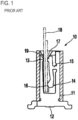
- Patent Literature 1 discloses a connector for film wire that has multiple terminals inserted into a housing and fixed therein, and when a film wire is inserted into an insertion portion of the housing, contact pins on the film wire make close contact with contact portions of the terminals (see FIG. 1 ).
- Each terminal of the connector has the contact portion on one side and a seesaw member that makes seesaw movements about a center is integrally formed with the terminal at a location opposite the contact portion, such that the seesaw member makes seesaw movements with the film wire, thus stabilizing the fixation state of the film wire.
- the seesaw member is formed such that a pressurization portion thereof is located opposite the contact portion of the terminal. If the pressurization portion and the terminal deviate from their opposing arrangement due to some effect such as an attachment error with the terminal, or if a force that separates the contact pins on the film wire and the contact portions of the terminals is generated by prying or the like, stable continuity may not be achieved.
- an object of the present disclosure is to provide a connector that can achieve more stable connection.
- a connector includes: a housing including an insertion portion with a predefined width into which a mating connection unit having a plurality of mating terminals arrayed thereon can be inserted, and a base portion located at a predefined length from the insertion portion in an insertion direction, the insertion direction being a direction of inserting the mating connection unit; and a plurality of terminals, each including: a fixation portion with one end fixed to the base portion; an extension portion with one end being contiguous with the fixation portion and another end extending in a reverse insertion direction opposite the insertion direction; and a connection portion with one end being contiguous with the extension portion and another end extending in the reverse insertion direction, the connection portion being capable of establishing continuity with corresponding one of the mating terminals.
- the plurality of terminals are arrayed in a width direction, the width direction being a direction of a width of the housing.
- the connection portion of each of the plurality of terminals includes: a connecting base portion extending from the other end of the extension portion in an intersection direction intersecting the insertion direction and the width direction; a first arm extending from one end, on the intersection direction side, of the connecting base portion in the reverse insertion direction; and a second arm extending from another end, on the intersection direction side, of the connecting base portion in the reverse insertion direction.
- the first arm includes: a support portion extending from a predefined location on the first arm on an extension side to the second arm side in the intersection direction; a sub-arm formed of a first sub-arm extending from an end of the support portion on the extension side in the reverse insertion direction, and a second sub-arm extending from that end in the insertion direction; a first contact portion protruding from the first sub-arm to the second arm side; and a second contact portion protruding from the second sub-arm to the second arm side.
- the second arm includes a pressing portion protruding toward a predefined location between the first contact portion and the second contact portion.
- connection portion of each of the plurality of terminals is configured such that when the mating connection unit is inserted between the respective first arms and the respective second arms via the insertion portion, the pressing portion presses against the mating connection unit and at least either contact portion of the first contact portion and the second contact portion establishes continuity with the mating connection unit.
- the connector of the present embodiment can achieve stable connection.
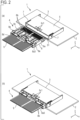
- FIG. 2 is a perspective view showing a printed circuit board 1 and a mating connection unit 4 according to the present embodiment, where FIG. 2(a) shows a state before the mating connection unit 4 is inserted into a connector 3 and FIG. 2(b) shows a state after insertion of the mating connection unit 4 into the connector 3 is completed.
- the mating connection unit 4 is formed of a flexible wiring board 9 and a mating insertion portion 8, as shown in FIG. 2 .
- FIG. 3 shows the flexible wiring board 9, where FIG. 3(a) is a plan view, FIG. 3(b) is a cross-sectional view at X-X, showing an electrode 9a and its vicinity enlarged, FIG. 3(c) is a front view of an end as seen from the electrode 9a side, and FIG. 3(d) is an enlarged view of region Y.
- the flexible wiring board 9 in the present embodiment is a thin-plate-shaped wiring board made of polyimide as base material, for example.
- the flexible wiring board 9 has flexibility enough to allow it to bend 180 degrees at its center or higher so that its opposite ends in a long direction (when represented with a coordinate axis, in the positive-negative direction on the y-axis illustrated in FIG. 3(a) ) are aligned with each other, for example.
- the flexible wiring board 9 in the present embodiment is formed of a first layer 91A and a second layer 91B as shown in FIG. 3(b) , the first layer 91A and the second layer 91B being integrally formed by bonding to one another with a certain adhesive.
- the flexible wiring board 9 is not limited to this structure. For example, it may be made of simple double layering, instead of integral formation.
- the first layer 91A has multiple wires 9A arrayed in a width direction of the flexible wiring board 9 (the right-left direction in FIG. 3(a) ), and an elongate electrode 9a for electrical connection with the connector 3 is provided at one end of each wire 9A.
- the wires 9A are covered with an insulation layer 9C for insulation.
- the second layer 91B has multiple wires 9B ( FIG. 3(b) ) arrayed in the width direction of the flexible wiring board 9 as with the first layer 91A, and an elongate electrode 9b for electrical connection with the connector 3 is provided at one end of each wire 9B.
- the wires 9B are covered with an insulation layer 9D for insulation.
- the multiple electrodes 9a and 9b are arranged offset (shifted) in the width direction of the flexible wiring board 9 from the positions at which they are opposite each other. This arrangement provides a staggered arrangement of the electrodes 9a and 9b, or multiple terminals, across the surface on the first layer 91A side and the surface on the second layer 91B side, as shown in FIG. 3(d) .
- the electrodes 9a, 9b serve as the terminals of the mating connection unit 4
- the electrodes 9a, 9b are also called “mating terminals" in the present embodiment.
- the flexible wiring board 9 has electrodes that are connectable to other apparatuses or devices at the end opposite the electrodes 9a, 9b (when represented with a coordinate axis, the positive direction side on the y-axis shown in FIG. 3(a) ).
- the electrodes connectable to other apparatuses or devices are not illustrated and only a part of the length of the flexible wiring board 9 is shown.
- the mating connection unit 4 includes the mating insertion portion 8 to facilitate insertion into the connector 3 at the end of the flexible wiring board 9 on the side of the electrodes 9a, 9b (when represented with a coordinate axis, the negative direction side on the y-axis shown in FIG. 2(a) ), as shown in FIG. 2(a) .
- Main components of the mating insertion portion 8 include an insertion guide 8a, tabs 8b, a lever 8c, and a secondary lock mechanism 8d.
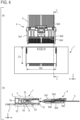
- FIG. 4(a) is a plan view of FIG. 2(a)
- FIG. 4(b) is a cross-sectional view of FIG. 4(a) at Z-Z.
- the insertion guide 8a is substantially box-shaped, having a shape of a hollow box into which the flexible wiring board 9 can be inserted. Specifically, as shown in FIGs. 4(a) and 4(b) , the insertion guide 8a has a substantially box-like shape with side walls 8a1, 8a2 standing on opposite side surfaces of the flexible wiring board 9, an upper cover 8a3 covering a top surface of the flexible wiring board 9, and a lower cover 8a4 covering a bottom surface of the flexible wiring board 9.
- the insertion guide 8a has an opening 8a5 on the opposite side of the electrodes 9a, 9b (when represented with a coordinate axis, the positive direction side on the y-axis shown in FIG.
- the insertion guide 8a thus has a shape of a hollow box inside it, allowing exposure of the electrodes 9a, 9b when the flexible wiring board 9 is placed inside the insertion guide 8a.
- the insertion guide 8a has a width length (the length in the right-left direction in FIG. 4(a) ) formed slightly shorter than an opening width of an insertion portion 51 of a housing 5.
- a height of the side walls 8a1, 8a2 is configured to be slightly shorter than the height of the insertion portion 51 so that the mating connection unit 4 can be inserted into the opening of the insertion portion 51. Tips of the side walls 8a1, 8a2 on the insertion side are tapered in order to help insertion into the connector 3.
- the insertion guide 8a thereby facilitates positioning in the width direction of the insertion portion 51 (when represented with a coordinate axis, the positive-negative direction on the x-axis shown in FIG.
- the mating insertion portion 8 has two tabs 8b on the upper cover 8a3 for fitting into (primary locking) lock holes 5c1 formed in the housing 5 of the connector 3, as shown in FIG. 2 . Fitting of the tabs 8b into the lock holes 5c1 prevents misalignment of fitting between the connector 3 and the mating connection unit 4.
- the mating insertion portion 8 has the secondary lock mechanism 8d on the upper cover 8a3 for further ensuring the fitting between the connector 3 and the mating connection unit 4.
- the mating connection unit 4 is fitted with the connector 3 by moving the mating connection unit 4 in a direction toward the connector 3 of the printed circuit board 1 (the same direction as an insertion direction P, discussed later) and inserting the mating insertion portion 8 of the mating connection unit 4 into the insertion portion 51 of the connector 3, as shown in FIG. 4(b) .
- the side walls 8a1, 8a2 are each provided with a positioning portion 8e ( FIG. 2(a) ) near the end opposite the tapered end.
- the positioning portion 8e limits insertion movement of the flexible wiring board 9 into the connector 3 such that the flexible wiring board 9 cannot be moved to a base portion 52 ( FIG. 4(b) ) side more than defined.
- FIG. 5 is an exploded perspective view of the printed circuit board 1. As shown in FIG. 5 , the main components of the printed circuit board 1 are a printed wiring board 2 and the connector 3 into which the mating connection unit 4 can be inserted.
- the printed wiring board 2 is made of glass epoxy resin as base material, for example, and on an upper surface 2a thereof, multiple electrodes 21A, 21B are arrayed in a longitudinal direction of the printed wiring board 2 (the direction of width length W3 in FIG. 4 ; hereinafter also referred to as "width direction W") so that electrical connection (hereinafter also referred to as "continuity") can be established with the electrodes 9a, 9b on the mating connection unit 4.
- the multiple electrodes 21A and electrodes 21B are arranged offset (shifted) in the width direction W from the positions at which they are opposite each other. This provides a staggered arrangement of the multiple electrodes 21A and electrodes 21B on the upper surface 2a of the printed wiring board 2.
- the printed wiring board 2 has two holes 22 into which fasteners 7 can be inserted through holes 54 in the connector 3.
- the main components of the connector 3 are the housing 5 and the multiple terminals 6, as shown in FIG. 5 .
- the housing 5 is a molded piece made of thermoplastic resin, for example, ABS, as base material, and is mounted on the upper surface 2a of the printed wiring board 2 in the present embodiment.
- the housing 5 of the present embodiment has side walls 5a, 5b, which are standing walls, and an upper surface 5c and a lower surface 5d covering portions of the side walls 5a, 5b, and forms a shape of a hollow box having the insertion portion 51, which is on the front side in FIG. 5 (when represented with a coordinate axis, the positive direction side on the y-axis shown in FIG. 5(a)), and the base portion 52, which is on the back side (when represented with a coordinate axis, the negative direction side on the y-axis shown in FIG. 5(a)).
- the insertion portion 51 has a rectangular opening formed in one end of the housing 5 and having a width length W3 ( FIG. 4(a) ), into which the mating connection unit 4 can be inserted.
- the base portion 52 has a rectangular opening with the same width length W3 as that of the opening in the insertion portion 51 at a location separated by a length D3 from the opening of the insertion portion 51 in the direction of inserting the mating connection unit 4, or when represented with a coordinate axis, in the negative direction on the y-axis shown in FIG. 4(b) (hereinafter also referred to as "insertion direction P").
- the housing 5 has multiple terminals 6 that are inserted in its hollow box-shaped interior, the terminals 6 being press-fit and fixed to the lower surface 5d of the housing 5. Details of the terminals 6 will be discussed later.
- the housing 5 has two lock holes 5c1 into which the tabs 8b of the mating insertion portion 8 are fitted, in the upper surface 5c near the center on the insertion portion 51 side.
- the housing 5 has multiple guide portions 53 in the hollow interior of the housing 5, the guide portions 53 being provided so as to extend (hereinafter also referred just as “to extend") in the direction from the base portion 52 toward the insertion portion 51, or when represented with a coordinate axis, in the positive direction on the y-axis shown in FIG. 4(b) (hereinafter also referred to as "reverse insertion direction P'").
- FIG. 6 is a diagram for describing a positional relationship between the terminals 6 and guide portions 53, where FIG.
- FIG. 6(a) is an enlarged view of region V in FIG. 4(b)
- FIG. 6(b) is a schematic diagram as seen from the insertion portion 51 side for describing arrangement in width direction W.
- FIG. 6(a) shows two terminals 6 (terminals 6A, 6B), and three guide portions 53 running in the vertical direction (when represented with a coordinate axis, in the positive-negative direction on the z-axis shown in FIG. 6(b) ).
- the guide portions 53 are hatched in order to distinguish between the terminals 6 and the guide portions 53.
- the guide portions 53 are thin plates and stand with their lengths horizontal. Each guide portion 53 is provided with a notch 53A into which the mating connection unit 4 can be inserted.
- the multiple guide portions 53 each have a similar configuration and are arranged in the width direction W (the right-left direction in FIG. 6(b) ) within the housing 5 such that the guide portions 53 and the terminals 6 alternate as shown in FIG. 6(b) .
- the multiple terminals 6 are made up of multiple terminals 6A arrayed in the width direction W of the connector 3 and establishing continuity with the electrodes 21A, and multiple terminals 6B arrayed in the width direction W of the connector 3 and establishing continuity with the electrodes 21B, as shown in FIG. 5 .
- FIG. 7 is a perspective view of the terminals 6. In FIG. 7 , only six terminals are illustrated as the multiple terminals 6 and the other terminals 6 are not shown.
- the connector 3 has the same number of terminals 6 as the total number of the electrodes 21A, 21B.
- the multiple terminals 6 are the terminals 6A as first terminals and the terminals 6B as second terminals, alternately arranged in the width direction W of the housing 5.
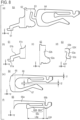
- FIG. 8 is a diagram defining formal regions for describing the configuration of the terminal 6A, where FIG. 8(a) shows an element constituting the entire terminal 6A, FIG. 8(b) shows an element constituting a contacting portion 61, FIG. 8(c) shows an element constituting a fixation portion 62, FIG. 8(d) shows an element constituting an extension portion 63, FIG. 8(e) shows an element constituting a connection portion 64, and FIG. 8(f) shows an element constituting a first arm 66.
- FIG. 9 is a diagram for describing the terminal 6A, where FIG. 9(a) is a perspective view and FIG. 9(b) is a plan view.
- the terminal 6A is formed of the contacting portion 61, the fixation portion 62, the extension portion 63, and the connection portion 64 as shown in FIG. 8(a) , and has a shape of a thin plate formed in one piece by punching, for example, with these portions contiguous with one another.
- the terminal 6A is made of electrically conductive material, such as copper, as base material.
- the contacting portion 61 is formed of a joining portion 61a to be electrically joined to an electrode 21A on the printed wiring board 2, a leg 61b which extends from one end of the joining portion 61a upward in the reverse insertion direction P' (the rightward direction in FIG. 8(b) ) and adjusts the length of the contacting portion 61, and a contacting end 61c extending from the leg 61b in the reverse insertion direction P' while having a predefined height greater than the width length of extension of the leg 61b, as shown in FIG. 8(b) .
- the fixation portion 62 is a thin plate contiguous with the contacting portion 61, as shown in FIG. 8(c) , and fixes the terminal 6 to the housing 5.
- the fixation portion 62 is formed of a fixing base portion 62a and a fixation extending portion 62b.
- the fixing base portion 62a has a shape of substantially square plate, is contiguous with the contacting end 61c on the insertion direction P side (the left side in FIG. 8(c) ), and has a fixed end 62a1 (see FIG. 9(b) ) to be press-fit and fixed to the base portion 52 of the housing 5 at a lower end (when represented with a coordinate axis, the end in the negative direction on the z-axis shown by FIG. 8(c) ).
- the fixation extending portion 62b forms a substantially rectangular plate extending from the upper surface 5c side of the fixing base portion 62a to the upper surface 5c side and having a width shorter than the width of the fixing base portion
- the extension portion 63 is a thin plate contiguous with the fixation portion 62 as shown in FIG. 8(d) , and adjusts application of pressure to the connection portion 64 caused by insertion of the flexible wiring board 9.
- the extension portion 63 has an extension base portion 63a, and extension ends 63b, 63c provided at opposite ends of the extension base portion 63a.
- the extension portion 63 extends in the reverse insertion direction P', with the extension end 63b contiguous with one end of the fixation extending portion 62b of the fixation portion 62.
- the extension base portion 63a extends from the other end of the extension end 63b over a predefined length in the direction of the lower surface 5d (the downward direction in FIG. 8(d) ).
- the extension end 63c extends from the end of the extension base portion 63a on the lower surface 5d side in the reverse insertion direction P' over a predefined length.
- an area of the extension portion 63 in which the direction of extension changes due to the extension base portion 63a and the extension end 63b will be called a "bent portion 63X”.
- an area in which the direction of extension changes due to the extension base portion 63a and the extension end 63c will be called a "bent portion 63Y”.
- the extension portion 63 is contiguous with the connection portion 64.
- the extension portion 63 is displaced as follows when the flexible wiring board 9 of the mating connection unit 4 is inserted into the connection portion 64.
- the extension base portion 63a rotates about the bent portion 63X as a fulcrum (is displaced clockwise in FIG. 9(b) ), and in conjunction with this movement, the bent portion 63Y and the extension end 63c are displaced in the insertion direction P (the direction toward the fixation portion 62) and the connection portion 64 is also displaced accordingly.
- the extension end 63c rotates about the bent portion 63Y as the fulcrum.
- the connection portion 64 is also displaced.
- the extension portion 63 has a first bent portion (the bent portion 63X) that allows at least part of the extension portion 63 to be displaced in the direction toward the fixation portion 62, and a second bent portion (the bent portion 63 Y) that allows at least part of the extension portion 63 to be displaced in the intersection direction I.
- the terminals 6 of the present disclosure may also be configured with either one bent portion of the bent portion 63X and the bent portion 63Y.
- the extension portion 63 adjusts application of pressure to the connection portion 64 by the flexible wiring board 9 via spring forces caused by the bent portions 63X, 63Y.
- the bent portions 63X, 63Y enable handling of contact position misalignment and angle mismatch due to, for example, deviation associated with press-fitting position of the terminals 6 to the housing 5 or manufacture errors of terminals, and can reduce insertion force in insertion of the flexible wiring board 9 into the connection portion 64, contributing to improved reliability by prevention of breakage.
- connection portion 64 has a thin plate shape with one end being contiguous with the extension end 63c of the extension portion 63 and the other end extending in the reverse insertion direction P'. As discussed later, the connection portion 64 is configured to be able to establish continuity with the mating connection unit 4 by insertion of the mating connection unit 4 into the connector 3.
- connection portion 64 is formed of a connecting base portion 65, a first arm 66, and a second arm 67 as shown in FIG. 8(e) .
- the connecting base portion 65 extends in the intersection direction I from the extension end 63c of the extension portion 63 and forms a substantially rectangular plate.
- the first arm 66 is formed of a main arm 66a, a support portion 66b, and a sub-arm 66c as shown in FIG. 8(f) .
- the main arm 66a linearly extends in the reverse insertion direction P' from the upper surface 5c side in the intersection direction I of the connecting base portion 65, and forms an elongate plate.
- the main arm 66a is shaped to taper as it goes in the extension direction.
- the support portion 66b extends from a predefined location on the main arm 66a at the extension side (although, in FIG.
- the sub-arm 66c is formed of a first sub-arm 66A extending from the end of the support portion 66b on the extension side to the reverse insertion direction P' side, and a second sub-arm 66B extending from the end of the support portion 66b on the extension side in the insertion direction P, as shown in FIG. 8(f) .
- a length of extension LA in the first sub-arm 66A ( FIG.
- the second sub-arm 66B has a lower spring constant than that of the first sub-arm 66A, such that the amount of displacement will be larger in the second sub-arm 66B than in the first sub-arm 66A when the flexible wiring board 9 is inserted. This enables reduced insertion force for inserting the flexible wiring board 9 into the mating connection unit 4.
- the first sub-arm 66A has a first contact portion 66Ap that protrudes to the second arm 67 side (the lower surface 5d side) in the intersection direction I, as shown in FIG. 9 .
- the first contact portion 66Ap is configured to be electrically connectable with an electrode on the flexible wiring board 9 by insertion of the mating connection unit 4 into the connector 3.
- the first sub-arm 66A has a first protrusion portion 66Ao that protrudes from the end on the insertion portion 51 side to the main arm 66a side (the upper surface 5c side) in the intersection direction I.
- the first protrusion portion 66Ao at least in part faces the neighboring guide portions 53 and overlaps them in the width direction W at a predefined gap ( FIG. 6 ).
- a tip position of the end of the first protrusion portion 66Ao on the protrusion side is located on the sub-arm 66c side (the lower surface 5d side) at a length t1 with respect to the position of the main arm 66a on the upper surface 5c side in the intersection direction I ( FIG. 8(e) ). Since the first arm 66 has spring property, it moves in the intersection direction I upon insertion of the flexible wiring board 9. When a force in the upward direction (the direction of the upper surface 5c) occurs on the first arm 66, the first arm 66 moves in the upward direction (the direction of the upper surface 5c).
- the main arm 66a being located on the upper surface 5c side at the length t1 relative to the first protrusion portion 66Ao serves as a clearance for enabling seesaw movements of the sub-arm 66c.
- the end of the first sub-arm 66A on the extension side has a slope portion 66As as a second slope portion, which is inclined to the main arm 66a side (the upper surface 5c side) in the intersection direction I as it goes in the reverse insertion direction P' starting at the first contact portion 66Ap.
- the second sub-arm 66B has a second contact portion 66Bp that protrudes to the second arm 67 side (the lower surface 5d side) in the intersection direction I, as shown in FIG. 9 .
- the second contact portion 66Bp is configured to be electrically connectable with an electrode on the flexible wiring board 9 by insertion of the mating connection unit 4 into the connector 3.
- the second sub-arm 66B has a second protrusion portion 66Bo that protrudes from the end on the extension side (the base portion 52 side) toward the main arm 66a (the upper surface 5c side).
- the second protrusion portion 66Bo at least in part faces the neighboring guide portions 53 and overlaps them in the width direction W at a predefined gap ( FIG. 6 ).
- the second protrusion portion 66Bo and the main arm 66a are located at a predefined distance from each other in the intersection direction I.
- the main arm 66a is provided with a recess 66H at a location opposite the second protrusion portion 66Bo in order to avoid contact with the second protrusion portion 66Bo, as shown in FIG. 9 .
- the end of the second sub-arm 66B on the extension side (the base portion 52 side) has a slope portion 66Bs as a third slope portion, which is inclined to the main arm 66a side (the upper surface 5c side) in the intersection direction I as it goes in the reverse insertion direction P' starting at the second contact portion 66Bp.
- the second arm 67 extends from the lower side in the intersection direction I of the connecting base portion 65 (the lower surface 5d side) in the reverse insertion direction P' and forms an elongate plate.
- the second arm 67 has a tapered shape and extends in the reverse insertion direction P' up to some midpoint in the extension direction and, on the further extension side, extends such that its tip is inclined to the upper surface 5c side as it extends in the reverse insertion direction P'. This increases the spring constant of the second arm 67.
- the first arm 66 has a seesaw structure with the linear main arm 66a, the support portion 66b, and the sub-arm 66c, and the spring constant of the first arm 66 is set lower than that of the second arm 67.
- the connecting base portion 65 is contiguous with the extension end 63c at its end on the extension end 63c side (the left side in FIG. 9(b) ).
- the position where they are contiguous is a predefined location between the end on the upper side (the upper surface 5c side) and the end on the lower side (the lower surface 5d side) of the connecting base portion 65 in the intersection direction I. Although, in FIG. 9 , this position is provided in a central portion, this is not limitative.
- the second arm 67 has a pressing portion 67p on the extension side as shown in FIG. 9(b) .
- the pressing portion 67p protrudes toward a predefined location between the first contact portion 66Ap and the second contact portion 66Bp in the sub-arm 66c.
- the pressing portion 67p in the present embodiment is located opposite some portion (G) of the second sub-arm 66B.
- G some portion of the second sub-arm 66B.
- the position of this G is determined so that a moment acting on the first contact portion 66Ap and a moment acting on the second contact portion 66Bp are balanced, in consideration of the seesaw structure formed by the sub-arm 66c and the like, lengths LAp and LBp ( FIG.
- the position of G can be set at a location on the second contact portion 66Bp side, rather than the center location between the first contact portion 66Ap and the second contact portion 66Bp, for example.
- the pressing portion 67p presses against the flexible wiring board 9 of the inserted mating connection unit 4.
- the end of the second arm 67 on the insertion portion 51 side (the side on which the second arm 67 extends) has a slope portion 67s as a first slope portion, which is inclined away from the sub-arm 66c (to the lower surface 5d side) as it goes to the insertion portion 51 side (to the reverse insertion direction P' side) starting at the pressing portion 67p.
- the end of the second arm 67 on the insertion portion 51 side at least in part faces the neighboring guide portions 53 and overlaps them in the width direction W at a predefined gap ( FIG. 6 ). This limits movement of the end of the second arm 67 on the insertion portion 51 side in the width direction W.
- the pressing portion 67p and the first contact portion 66Ap are at a length t2 from one another in the intersection direction I, and the pressing portion 67p and the second contact portion 66Bp are at a length t3 from one another in the intersection direction I ( FIG. 8(e) ).
- t2 and t3 are set slightly smaller than the thickness of the flexible wiring board 9 in order to enable insertion of the flexible wiring board 9 and to appropriately secure pressing force with the pressing portion 67p and contact force of the first contact portion 66Ap and the second contact portion 66Bp with the flexible wiring board 9.
- t2 and t3 are not limited to it and may be set to other lengths for the purpose of increasing the contact pressure with the flexible wiring board 9.
- t2 and t3 may be designed to be 0 (zero) or negative (that is, in FIG. 8(e) , the position of the pressing portion 67p in the intersection direction I is on the upper surface 5c side relative to the first contact portion 66Ap or the second contact portion 66Bp), for example.
- FIG. 10 is a diagram for describing the terminal 6B, where FIG. 10(a) is a perspective view and FIG. 10(b) is a plan view.
- the terminal 6B is formed of a contacting portion 61B, the fixation portion 62, the extension portion 63, and a connection portion 64B as shown in FIG. 10 .
- the contacting portion 61B does not have portions corresponding to the leg 61b and the contacting end 61c of the contacting portion 61 ( FIG. 8(b) ); it is formed in a shape similar to the joining portion 61a and is electrically joined with an electrode 21B on the printed wiring board 2.
- the fixation portion 62 and the extension portion 63 of the terminal 6B have the same shapes as the fixation portion 62 and the extension portion 63 of the terminal 6A.
- connection portion 64B has the same configuration of that of the connection portion 64 of the terminal 6A. However, the connection portion 64B has the same shape as the connection portion 64 of the terminal 6A but inverted (rotated 180 degrees) about the insertion direction P, and is contiguous with the extension portion 63 of the terminal 6B. Due to this inversion, the terminal 6B is configured with the pressing portion 67p on the upper surface 5c side and the first contact portion 66Ap and the second contact portion 66Bp on the lower surface 5d side.
- the respective first contact portions 66Ap are arrayed at positions that overlap in the width direction W
- the respective second contact portions 66Bp are arrayed at positions that overlap in the width direction W
- the respective pressing portions 67p are arrayed at positions that overlap in the width direction W.
- the respective first contact portions 66Ap are arrayed at positions that overlap in the width direction W
- the respective second contact portions 66Bp are arrayed at positions that overlap in the width direction W
- the respective pressing portions 67p are arrayed at positions that overlap in the width direction W.
- a process of mounting the connector 3 to the printed wiring board 2 to obtain the printed circuit board 1 can be performed in the following steps, for example (see FIG. 5 ).
- Solder paste is applied to the electrodes 21A, 21B on the printed wiring board 2.
- the terminals 6A of the connector 3 and the electrodes 21A on the printed wiring board 2 are placed opposite each other, the terminals 6B of the connector 3 and the electrodes 21B on the printed wiring board 2 are placed opposite each other, and the holes 54 in the housing 5 are aligned with the holes 22 in the printed wiring board 2.
- the fasteners 7 are inserted from above (through the upper surface 5c) to fix the printed wiring board 2 and the connector 3 to each other. In this state, they are subjected to heating treatment in a reflow furnace, for example, and electrical joining between the terminal 6 and the printed wiring board 2 is completed, providing the printed circuit board 1.
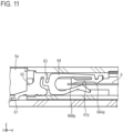
- FIG. 11 shows a situation where the mating connection unit 4 is inserted in FIG. 6(a) .
- the illustration of FIG. 11 only adds a representation of the flexible wiring board 9 to FIG. 6(a) .
- the description below is for the case where the printed circuit board 1 with the connector 3 is fixed (is at rest) and the mating connection unit 4 is moved in the insertion direction P to be inserted into it (the case shown in FIG. 4(b) ).
- the height of the side wall 8a1 of the mating insertion portion 8 is set slightly smaller than the height of the insertion portion 51, and the tip of the flexible wiring board 9 is inserted so as to be guided to a location exactly between the first contact portion 66Ap and the pressing portion 67p in the intersection direction I.
- the terminals 6A, 6B would behave as described below because the terminals 6A, 6B have slope portions (the slope portion 66As, the slope portion 67s, the slope portion 66Bs).
- the first arm 66 In a case where the tip of the flexible wiring board 9 makes contact with the slope portions 66As, if the tip of the flexible wiring board 9 makes contact with the terminals 6A, the first arm 66 would move to the upper side (the upper surface 5c side), and if the tip of the flexible wiring board 9 makes contact with the terminals 6B, the first arm 66 would move to the lower side (the lower surface 5d side). At the same time, the sub-arm 66c tilts so that the second contact portion 66Bp moves away from the main arm 66a (in other words, the sub-arm 66c tilts so that the first contact portion 66Ap comes closer to the main arm 66a).
- the second arm 67 would move to the lower side (the lower surface 5d side), and if the tip of the flexible wiring board 9 makes contact with the terminals 6B, the second arm 67 would move to the upper side (the upper surface 5c side).
- the sub-arm 66c tilts so that the second contact portion 66Bp comes closer to the main arm 66a (in other words, the sub-arm 66c tilts so that the first contact portion 66Ap moves away from the main arm 66a). That is to say, the structure is such that the terminals 6 are less prone to buckling during insertion of the flexible wiring board 9 into the terminals 6.
- the tip of the flexible wiring board 9 is stably inserted near the connecting base portion 65 as shown in FIG. 11 .
- By moving the secondary lock mechanism 8d in the insertion direction P secondary locking is activated, completing the insertion of the mating connection unit 4.
- the mating connection unit 4 is pressed by the pressing portion 67p when the mating connection unit 4 is inserted between the sub-arm 66c and the second arm 67.
- the electrodes 9a, 9b make contact with the opposing first contact portions 66Ap and second contact portions 66Bp, respectively, producing a reaction to the pressing force.
- the flexible wiring board 9 when focusing on one wire and one electrode, for example, a wire 9A and an electrode 9a, the flexible wiring board 9 takes the form of a beam supported at both ends, with one surface supported by the first contact portion 66Ap and the second contact portion 66Bp and the other surface pressed by the pressing portion 67p.
- the pressing portion 67p since the pressing portion 67p is not provided at a location opposite the first contact portion 66Ap or the second contact portion 66Bp, the pressing force of the pressing portion 67p will not be concentrated at either one of the contact portions. Thus, it is possible to reduce insertion force for the flexible wiring board 9. This can reduce damage to the flexible wiring board 9 and increase the reliability of the connection between the first contact portions 66Ap and the electrodes 9a, 9b and the connection between the second contact portions 66Bp and the electrodes 9a, 9b.
- the first arm 66 has a so-called seesaw structure formed by the support portion 66b and the sub-arm 66c, and the spring constant of the first arm 66 is set lower than that of the second arm 67.
- This seesaw structure can also enable reduction in insertion force for the flexible wiring board 9 and prevent damage to the flexible wiring board 9.
- the direction of pressing the flexible wiring board 9 alternates between being upward and downward, as seen from the width direction W.
- a force such as tilting acts on the flexible wiring board 9.
- connection portion 64 of each of the multiple terminals 6 is configured such that when the mating connection unit 4 is inserted between the respective first arms 66 and second arms 67 via the insertion portion 51, the pressing portion 67p presses against the mating connection unit 4 and at least either contact portion of the first contact portion 66Ap and the second contact portion 66Bp establishes continuity with the mating connection unit 4. This enables stable connection.
- FIG. 12 is a perspective view of multiple terminals 6' uniformly configured in the same shape.
- the connector 3 in the present embodiment may use multiple terminals 6' composed only of either type of terminals as shown in FIG. 12 (in FIG. 12 , the terminals 6B).
- a mating connection unit 4 carrying the wires 9B and the electrodes 9b from the wires 9A, 9B and the electrodes 9a, 9b in FIG. 3 is prepared.
- a mating connection unit 4 including a flexible wiring board (flexible wiring board 9', not illustrated) with wires and electrodes only on one surface is prepared.
- a reaction to a pressing force sufficient for continuity with at least one of the first contact portion 66Ap and the second contact portion 66Bp will also occur on the mating connection unit 4, enabling continuity with the mating connection unit 4.
- continuity via the other contact portion is possible, and thus improved reliability of connection with the mating connection unit 4 is expected.
Landscapes
- Coupling Device And Connection With Printed Circuit (AREA)
- Details Of Connecting Devices For Male And Female Coupling (AREA)
Abstract
Description
- The present disclosure relates to structures of connectors.
- One conventional technique for connectors is to construct a connector for connecting a film wire to a board with no flips on the connector and to insert the film wire into the housing of the connector with a small force at the beginning and a large force only at the end to fix the film wire. This can prevent damage to or breakage of contact pins disposed on the film wire and also allows the film wire to be inserted at correct locations on terminals, stabilizing the fixation state of the film wire (see
Japanese Patent Application Laid Open No. 2008-504645 Patent Literature 1"), for instance).Patent Literature 1 discloses a connector for film wire that has multiple terminals inserted into a housing and fixed therein, and when a film wire is inserted into an insertion portion of the housing, contact pins on the film wire make close contact with contact portions of the terminals (seeFIG. 1 ). Each terminal of the connector has the contact portion on one side and a seesaw member that makes seesaw movements about a center is integrally formed with the terminal at a location opposite the contact portion, such that the seesaw member makes seesaw movements with the film wire, thus stabilizing the fixation state of the film wire. - In the connector of
Patent Literature 1, however, the seesaw member is formed such that a pressurization portion thereof is located opposite the contact portion of the terminal. If the pressurization portion and the terminal deviate from their opposing arrangement due to some effect such as an attachment error with the terminal, or if a force that separates the contact pins on the film wire and the contact portions of the terminals is generated by prying or the like, stable continuity may not be achieved. - In view of the foregoing problem, an object of the present disclosure is to provide a connector that can achieve more stable connection.
- To solve the above-described problem, a connector according to the present embodiment includes: a housing including an insertion portion with a predefined width into which a mating connection unit having a plurality of mating terminals arrayed thereon can be inserted, and a base portion located at a predefined length from the insertion portion in an insertion direction, the insertion direction being a direction of inserting the mating connection unit; and a plurality of terminals, each including: a fixation portion with one end fixed to the base portion; an extension portion with one end being contiguous with the fixation portion and another end extending in a reverse insertion direction opposite the insertion direction; and a connection portion with one end being contiguous with the extension portion and another end extending in the reverse insertion direction, the connection portion being capable of establishing continuity with corresponding one of the mating terminals. The plurality of terminals are arrayed in a width direction, the width direction being a direction of a width of the housing. The connection portion of each of the plurality of terminals includes: a connecting base portion extending from the other end of the extension portion in an intersection direction intersecting the insertion direction and the width direction; a first arm extending from one end, on the intersection direction side, of the connecting base portion in the reverse insertion direction; and a second arm extending from another end, on the intersection direction side, of the connecting base portion in the reverse insertion direction. The first arm includes: a support portion extending from a predefined location on the first arm on an extension side to the second arm side in the intersection direction; a sub-arm formed of a first sub-arm extending from an end of the support portion on the extension side in the reverse insertion direction, and a second sub-arm extending from that end in the insertion direction; a first contact portion protruding from the first sub-arm to the second arm side; and a second contact portion protruding from the second sub-arm to the second arm side. The second arm includes a pressing portion protruding toward a predefined location between the first contact portion and the second contact portion. The connection portion of each of the plurality of terminals is configured such that when the mating connection unit is inserted between the respective first arms and the respective second arms via the insertion portion, the pressing portion presses against the mating connection unit and at least either contact portion of the first contact portion and the second contact portion establishes continuity with the mating connection unit.
- The connector of the present embodiment can achieve stable connection.
-
-
FIG. 1 is a diagram for describing a conventional art of a connector. -
FIG. 2 is a perspective view showing a printedcircuit board 1 and amating connection unit 4 according to the present embodiment, whereFIG. 2(a) shows a state before themating connection unit 4 is inserted into aconnector 3 andFIG. 2(b) shows a state after insertion of themating connection unit 4 into theconnector 3 is completed. -
FIG. 3 shows aflexible wiring board 9, whereFIG. 3(a) is a plan view,FIG. 3(b) is a cross-sectional view at X-X, showing anelectrode 9a and its vicinity enlarged,FIG. 3(c) is a front view of an end as seen from theelectrode 9a side, andFIG. 3(d) is an enlarged view of region Y. -
FIG. 4(a) is a plan view ofFIG. 2(a) , andFIG. 4(b) is a cross-sectional view ofFIG. 4(a) at Z-Z. -
FIG. 5 is an exploded perspective view of the printedcircuit board 1. -
FIG. 6 is a diagram for describing a positional relationship betweenterminals 6 andguide portions 53, whereFIG. 6(a) is an enlarged view of region V inFIG. 4(b) , andFIG. 6(b) is a schematic diagram as seen from theinsertion portion 51 side for describing arrangement in width direction W. -
FIG. 7 is a perspective view ofterminals 6. -
FIG. 8 is a diagram defining formal regions for describing the configuration of aterminal 6A, whereFIG. 8(a) shows an element constituting theentire terminal 6A,FIG. 8(b) shows an element constituting a contactingportion 61,FIG. 8(c) shows an element constituting afixation portion 62,FIG. 8(d) shows an element constituting anextension portion 63,FIG. 8(e) shows an element constituting aconnection portion 64, andFIG. 8(f) shows an element constituting afirst arm 66. -
FIG. 9 is a diagram for describing theterminal 6A, whereFIG. 9(a) is a perspective view andFIG. 9(b) is a plan view. -
FIG. 10 is a diagram for describing aterminal 6B, whereFIG. 10(a) is a perspective view andFIG. 10(b) is a plan view. -
FIG. 11 shows a situation where themating connection unit 4 is inserted inFIG. 6(a) . -
FIG. 12 is a perspective view of multiple terminals 6' uniformly configured in the same shape. - An embodiment of the present disclosure is described below with reference to drawings. In the description that follows, components with the same function are denoted with the same reference characters and overlapping description is omitted.
-
FIG. 2 is a perspective view showing a printedcircuit board 1 and amating connection unit 4 according to the present embodiment, whereFIG. 2(a) shows a state before themating connection unit 4 is inserted into aconnector 3 andFIG. 2(b) shows a state after insertion of themating connection unit 4 into theconnector 3 is completed. - The
mating connection unit 4 according to the present embodiment is formed of aflexible wiring board 9 and a mating insertion portion 8, as shown inFIG. 2 .FIG. 3 shows theflexible wiring board 9, whereFIG. 3(a) is a plan view,FIG. 3(b) is a cross-sectional view at X-X, showing anelectrode 9a and its vicinity enlarged,FIG. 3(c) is a front view of an end as seen from theelectrode 9a side, andFIG. 3(d) is an enlarged view of region Y. Theflexible wiring board 9 in the present embodiment is a thin-plate-shaped wiring board made of polyimide as base material, for example. Theflexible wiring board 9 has flexibility enough to allow it to bend 180 degrees at its center or higher so that its opposite ends in a long direction (when represented with a coordinate axis, in the positive-negative direction on the y-axis illustrated inFIG. 3(a) ) are aligned with each other, for example. Theflexible wiring board 9 in the present embodiment is formed of afirst layer 91A and asecond layer 91B as shown inFIG. 3(b) , thefirst layer 91A and thesecond layer 91B being integrally formed by bonding to one another with a certain adhesive. However, theflexible wiring board 9 is not limited to this structure. For example, it may be made of simple double layering, instead of integral formation. Thefirst layer 91A hasmultiple wires 9A arrayed in a width direction of the flexible wiring board 9 (the right-left direction inFIG. 3(a) ), and anelongate electrode 9a for electrical connection with theconnector 3 is provided at one end of eachwire 9A. Thewires 9A are covered with aninsulation layer 9C for insulation. Thesecond layer 91B hasmultiple wires 9B (FIG. 3(b) ) arrayed in the width direction of theflexible wiring board 9 as with thefirst layer 91A, and anelongate electrode 9b for electrical connection with theconnector 3 is provided at one end of eachwire 9B. Thewires 9B are covered with aninsulation layer 9D for insulation. Themultiple electrodes flexible wiring board 9 from the positions at which they are opposite each other. This arrangement provides a staggered arrangement of theelectrodes first layer 91A side and the surface on thesecond layer 91B side, as shown inFIG. 3(d) . As theelectrodes mating connection unit 4, theelectrodes - The
flexible wiring board 9 has electrodes that are connectable to other apparatuses or devices at the end opposite theelectrodes FIG. 3(a) ). InFIGs. 2 to 4 , the electrodes connectable to other apparatuses or devices are not illustrated and only a part of the length of theflexible wiring board 9 is shown. - The
mating connection unit 4 includes the mating insertion portion 8 to facilitate insertion into theconnector 3 at the end of theflexible wiring board 9 on the side of theelectrodes FIG. 2(a) ), as shown inFIG. 2(a) . Main components of the mating insertion portion 8 include aninsertion guide 8a,tabs 8b, alever 8c, and asecondary lock mechanism 8d.FIG. 4(a) is a plan view ofFIG. 2(a) , andFIG. 4(b) is a cross-sectional view ofFIG. 4(a) at Z-Z. Theinsertion guide 8a is substantially box-shaped, having a shape of a hollow box into which theflexible wiring board 9 can be inserted. Specifically, as shown inFIGs. 4(a) and 4(b) , theinsertion guide 8a has a substantially box-like shape with side walls 8a1, 8a2 standing on opposite side surfaces of theflexible wiring board 9, an upper cover 8a3 covering a top surface of theflexible wiring board 9, and a lower cover 8a4 covering a bottom surface of theflexible wiring board 9. Theinsertion guide 8a has an opening 8a5 on the opposite side of theelectrodes FIG. 4(b) ), and an opening 8a6 on the side of theelectrodes FIG. 4(b) ). The side walls 8a1, 8a2 extend to the side of theelectrodes FIG. 4(b) ) further than the upper cover 8a3 and the lower cover 8a4 so as to cover both ends of theflexible wiring board 9 in the width direction. Theinsertion guide 8a thus has a shape of a hollow box inside it, allowing exposure of theelectrodes flexible wiring board 9 is placed inside theinsertion guide 8a. Theinsertion guide 8a has a width length (the length in the right-left direction inFIG. 4(a) ) formed slightly shorter than an opening width of aninsertion portion 51 of ahousing 5. A height of the side walls 8a1, 8a2 is configured to be slightly shorter than the height of theinsertion portion 51 so that themating connection unit 4 can be inserted into the opening of theinsertion portion 51. Tips of the side walls 8a1, 8a2 on the insertion side are tapered in order to help insertion into theconnector 3. Theinsertion guide 8a thereby facilitates positioning in the width direction of the insertion portion 51 (when represented with a coordinate axis, the positive-negative direction on the x-axis shown inFIG. 4(a) ) and in the vertical direction (the height direction; when represented with a coordinate axis, the positive-negative direction on the z-axis shown inFIG. 4(b) ), and facilitates insertion of themating connection unit 4 into theconnector 3. - The mating insertion portion 8 has two
tabs 8b on the upper cover 8a3 for fitting into (primary locking) lock holes 5c1 formed in thehousing 5 of theconnector 3, as shown inFIG. 2 . Fitting of thetabs 8b into the lock holes 5c1 prevents misalignment of fitting between theconnector 3 and themating connection unit 4. The mating insertion portion 8 has thesecondary lock mechanism 8d on the upper cover 8a3 for further ensuring the fitting between theconnector 3 and themating connection unit 4. Assuming that the printedcircuit board 1 is at rest, themating connection unit 4 is fitted with theconnector 3 by moving themating connection unit 4 in a direction toward theconnector 3 of the printed circuit board 1 (the same direction as an insertion direction P, discussed later) and inserting the mating insertion portion 8 of themating connection unit 4 into theinsertion portion 51 of theconnector 3, as shown inFIG. 4(b) . The side walls 8a1, 8a2 are each provided with apositioning portion 8e (FIG. 2(a) ) near the end opposite the tapered end. Thepositioning portion 8e limits insertion movement of theflexible wiring board 9 into theconnector 3 such that theflexible wiring board 9 cannot be moved to a base portion 52 (FIG. 4(b) ) side more than defined. This prevents breakage ofterminals 6 in theconnector 3 and theflexible wiring board 9, for example. After fitting of thetabs 8b and the lock holes 5c1 is completed, thesecondary lock mechanism 8d is pushed in the insertion direction P, causing portions of projections (not shown) provided at the opposite ends of thesecondary lock mechanism 8d to slide under thelever 8c. This prohibits thelever 8c from being pushed downward (to the lower cover 8a4 side) and hence it becomes impossible to release the primary locking, completing secondary lock (secondary locking). This motion can make the user aware that theconnector 3 has been connected with themating connection unit 4 reliably, not only functionally but visually and perceptually. The upper cover 8a3 has thelever 8c (FIG. 2 ) provided contiguously with thetabs 8b. By moving thesecondary lock mechanism 8d in a reverse insertion direction P', which will be discussed later, the secondary locking is released and thelever 8c can move downward (to the lower cover 8a4 side). When thelever 8c is pushed downward, thetabs 8b move down correspondingly, releasing the fitting between thetabs 8b and the lock holes 5c1 (the primary locking). -
FIG. 5 is an exploded perspective view of the printedcircuit board 1. As shown inFIG. 5 , the main components of the printedcircuit board 1 are a printedwiring board 2 and theconnector 3 into which themating connection unit 4 can be inserted. - The printed
wiring board 2 is made of glass epoxy resin as base material, for example, and on anupper surface 2a thereof,multiple electrodes FIG. 4 ; hereinafter also referred to as "width direction W") so that electrical connection (hereinafter also referred to as "continuity") can be established with theelectrodes mating connection unit 4. Themultiple electrodes 21A andelectrodes 21B are arranged offset (shifted) in the width direction W from the positions at which they are opposite each other. This provides a staggered arrangement of themultiple electrodes 21A andelectrodes 21B on theupper surface 2a of the printedwiring board 2. The printedwiring board 2 has twoholes 22 into whichfasteners 7 can be inserted throughholes 54 in theconnector 3. - The main components of the
connector 3 are thehousing 5 and themultiple terminals 6, as shown inFIG. 5 . - The
housing 5 is a molded piece made of thermoplastic resin, for example, ABS, as base material, and is mounted on theupper surface 2a of the printedwiring board 2 in the present embodiment. Thehousing 5 of the present embodiment hasside walls upper surface 5c and alower surface 5d covering portions of theside walls insertion portion 51, which is on the front side inFIG. 5 (when represented with a coordinate axis, the positive direction side on the y-axis shown in FIG. 5(a)), and thebase portion 52, which is on the back side (when represented with a coordinate axis, the negative direction side on the y-axis shown in FIG. 5(a)). Theinsertion portion 51 has a rectangular opening formed in one end of thehousing 5 and having a width length W3 (FIG. 4(a) ), into which themating connection unit 4 can be inserted. Thebase portion 52 has a rectangular opening with the same width length W3 as that of the opening in theinsertion portion 51 at a location separated by a length D3 from the opening of theinsertion portion 51 in the direction of inserting themating connection unit 4, or when represented with a coordinate axis, in the negative direction on the y-axis shown inFIG. 4(b) (hereinafter also referred to as "insertion direction P"). Thehousing 5 hasmultiple terminals 6 that are inserted in its hollow box-shaped interior, theterminals 6 being press-fit and fixed to thelower surface 5d of thehousing 5. Details of theterminals 6 will be discussed later. - The
housing 5 has two lock holes 5c1 into which thetabs 8b of the mating insertion portion 8 are fitted, in theupper surface 5c near the center on theinsertion portion 51 side. As shown inFIG. 4 , thehousing 5 hasmultiple guide portions 53 in the hollow interior of thehousing 5, theguide portions 53 being provided so as to extend (hereinafter also referred just as "to extend") in the direction from thebase portion 52 toward theinsertion portion 51, or when represented with a coordinate axis, in the positive direction on the y-axis shown inFIG. 4(b) (hereinafter also referred to as "reverse insertion direction P'").FIG. 6 is a diagram for describing a positional relationship between theterminals 6 and guideportions 53, whereFIG. 6(a) is an enlarged view of region V inFIG. 4(b) , andFIG. 6(b) is a schematic diagram as seen from theinsertion portion 51 side for describing arrangement in width direction W. For facilitating understanding of the structure, oneterminal 6 and oneguide portion 53 are shown inFIG. 6(a). FIG. 6(b) shows two terminals 6 (terminals guide portions 53 running in the vertical direction (when represented with a coordinate axis, in the positive-negative direction on the z-axis shown inFIG. 6(b) ). InFIG. 6(b) , theguide portions 53 are hatched in order to distinguish between theterminals 6 and theguide portions 53. As shown inFIG. 6 , theguide portions 53 are thin plates and stand with their lengths horizontal. Eachguide portion 53 is provided with anotch 53A into which themating connection unit 4 can be inserted. Themultiple guide portions 53 each have a similar configuration and are arranged in the width direction W (the right-left direction inFIG. 6(b) ) within thehousing 5 such that theguide portions 53 and theterminals 6 alternate as shown inFIG. 6(b) . - The
multiple terminals 6 are made up ofmultiple terminals 6A arrayed in the width direction W of theconnector 3 and establishing continuity with theelectrodes 21A, andmultiple terminals 6B arrayed in the width direction W of theconnector 3 and establishing continuity with theelectrodes 21B, as shown inFIG. 5 .FIG. 7 is a perspective view of theterminals 6. InFIG. 7 , only six terminals are illustrated as themultiple terminals 6 and theother terminals 6 are not shown. Theconnector 3 has the same number ofterminals 6 as the total number of theelectrodes multiple terminals 6 are theterminals 6A as first terminals and theterminals 6B as second terminals, alternately arranged in the width direction W of thehousing 5. -
FIG. 8 is a diagram defining formal regions for describing the configuration of theterminal 6A, whereFIG. 8(a) shows an element constituting theentire terminal 6A,FIG. 8(b) shows an element constituting a contactingportion 61,FIG. 8(c) shows an element constituting afixation portion 62,FIG. 8(d) shows an element constituting anextension portion 63,FIG. 8(e) shows an element constituting aconnection portion 64, andFIG. 8(f) shows an element constituting afirst arm 66.FIG. 9 is a diagram for describing theterminal 6A, whereFIG. 9(a) is a perspective view andFIG. 9(b) is a plan view. Theterminal 6A is formed of the contactingportion 61, thefixation portion 62, theextension portion 63, and theconnection portion 64 as shown inFIG. 8(a) , and has a shape of a thin plate formed in one piece by punching, for example, with these portions contiguous with one another. The terminal 6A is made of electrically conductive material, such as copper, as base material. - The contacting
portion 61 is formed of a joiningportion 61a to be electrically joined to anelectrode 21A on the printedwiring board 2, aleg 61b which extends from one end of the joiningportion 61a upward in the reverse insertion direction P' (the rightward direction inFIG. 8(b) ) and adjusts the length of the contactingportion 61, and a contactingend 61c extending from theleg 61b in the reverse insertion direction P' while having a predefined height greater than the width length of extension of theleg 61b, as shown inFIG. 8(b) . - The
fixation portion 62 is a thin plate contiguous with the contactingportion 61, as shown inFIG. 8(c) , and fixes theterminal 6 to thehousing 5. Thefixation portion 62 is formed of a fixingbase portion 62a and afixation extending portion 62b. The fixingbase portion 62a has a shape of substantially square plate, is contiguous with the contactingend 61c on the insertion direction P side (the left side inFIG. 8(c) ), and has a fixed end 62a1 (seeFIG. 9(b) ) to be press-fit and fixed to thebase portion 52 of thehousing 5 at a lower end (when represented with a coordinate axis, the end in the negative direction on the z-axis shown byFIG. 8(c) ). Thefixation extending portion 62b forms a substantially rectangular plate extending from theupper surface 5c side of the fixingbase portion 62a to theupper surface 5c side and having a width shorter than the width of the fixingbase portion 62a. - The
extension portion 63 is a thin plate contiguous with thefixation portion 62 as shown inFIG. 8(d) , and adjusts application of pressure to theconnection portion 64 caused by insertion of theflexible wiring board 9. Theextension portion 63 has anextension base portion 63a, and extension ends 63b, 63c provided at opposite ends of theextension base portion 63a. Theextension portion 63 extends in the reverse insertion direction P', with theextension end 63b contiguous with one end of thefixation extending portion 62b of thefixation portion 62. Theextension base portion 63a extends from the other end of theextension end 63b over a predefined length in the direction of thelower surface 5d (the downward direction inFIG. 8(d) ). Theextension end 63c extends from the end of theextension base portion 63a on thelower surface 5d side in the reverse insertion direction P' over a predefined length. In the present embodiment, an area of theextension portion 63 in which the direction of extension changes due to theextension base portion 63a and theextension end 63b will be called a "bent portion 63X". Likewise, an area in which the direction of extension changes due to theextension base portion 63a and theextension end 63c will be called a "bent portion 63Y". Theextension portion 63 is contiguous with theconnection portion 64. Theextension portion 63 is displaced as follows when theflexible wiring board 9 of themating connection unit 4 is inserted into theconnection portion 64. For a force in the insertion direction P, theextension base portion 63a rotates about thebent portion 63X as a fulcrum (is displaced clockwise inFIG. 9(b) ), and in conjunction with this movement, thebent portion 63Y and theextension end 63c are displaced in the insertion direction P (the direction toward the fixation portion 62) and theconnection portion 64 is also displaced accordingly. For a force in a direction that intersects substantially orthogonally both the insertion direction P and the width direction W (the vertical direction inFIG. 9(b) ; hereinafter also referred to as "intersection direction I"), theextension end 63c rotates about thebent portion 63Y as the fulcrum. Specifically, when the force in the intersection direction I is to the upper side (theupper surface 5c side), displacement occurs counterclockwise inFIG. 9(b) , and when the force in the intersection direction I is to the lower side (thelower surface 5d side), displacement occurs clockwise. This causes displacement of theextension end 63c in the intersection direction I. In conjunction with the displacement of theextension end 63c, theconnection portion 64 is also displaced. Specifically, theextension portion 63 has a first bent portion (thebent portion 63X) that allows at least part of theextension portion 63 to be displaced in the direction toward thefixation portion 62, and a second bent portion (thebent portion 63 Y) that allows at least part of theextension portion 63 to be displaced in the intersection direction I. Theterminals 6 of the present disclosure may also be configured with either one bent portion of thebent portion 63X and thebent portion 63Y. - Thus, the
extension portion 63 adjusts application of pressure to theconnection portion 64 by theflexible wiring board 9 via spring forces caused by thebent portions bent portions terminals 6 to thehousing 5 or manufacture errors of terminals, and can reduce insertion force in insertion of theflexible wiring board 9 into theconnection portion 64, contributing to improved reliability by prevention of breakage. - The
connection portion 64 has a thin plate shape with one end being contiguous with theextension end 63c of theextension portion 63 and the other end extending in the reverse insertion direction P'. As discussed later, theconnection portion 64 is configured to be able to establish continuity with themating connection unit 4 by insertion of themating connection unit 4 into theconnector 3. - The
connection portion 64 is formed of a connectingbase portion 65, afirst arm 66, and asecond arm 67 as shown inFIG. 8(e) . - The connecting
base portion 65 extends in the intersection direction I from theextension end 63c of theextension portion 63 and forms a substantially rectangular plate. - The
first arm 66 is formed of amain arm 66a, asupport portion 66b, and a sub-arm 66c as shown inFIG. 8(f) . Themain arm 66a linearly extends in the reverse insertion direction P' from theupper surface 5c side in the intersection direction I of the connectingbase portion 65, and forms an elongate plate. Themain arm 66a is shaped to taper as it goes in the extension direction. Thesupport portion 66b extends from a predefined location on themain arm 66a at the extension side (although, inFIG. 8(f) , it is an end of themain arm 66a, it is not limited to the end) to thesecond arm 67 side in the intersection direction I (thelower surface 5d side) for a very small length compared to the extension length of thefirst arm 66, and serves as the fulcrum for seesaw behaviors of the sub-arm 66c. The sub-arm 66c is formed of a first sub-arm 66A extending from the end of thesupport portion 66b on the extension side to the reverse insertion direction P' side, and a second sub-arm 66B extending from the end of thesupport portion 66b on the extension side in the insertion direction P, as shown inFIG. 8(f) . A length of extension LA in thefirst sub-arm 66A (FIG. 9 ) is set shorter than a length of extension LB in the second sub-arm 66B. As a result of this, the second sub-arm 66B has a lower spring constant than that of thefirst sub-arm 66A, such that the amount of displacement will be larger in the second sub-arm 66B than in thefirst sub-arm 66A when theflexible wiring board 9 is inserted. This enables reduced insertion force for inserting theflexible wiring board 9 into themating connection unit 4. - The
first sub-arm 66A has a first contact portion 66Ap that protrudes to thesecond arm 67 side (thelower surface 5d side) in the intersection direction I, as shown inFIG. 9 . The first contact portion 66Ap is configured to be electrically connectable with an electrode on theflexible wiring board 9 by insertion of themating connection unit 4 into theconnector 3. Thefirst sub-arm 66A has a first protrusion portion 66Ao that protrudes from the end on theinsertion portion 51 side to themain arm 66a side (theupper surface 5c side) in the intersection direction I. The first protrusion portion 66Ao at least in part faces the neighboringguide portions 53 and overlaps them in the width direction W at a predefined gap (FIG. 6 ). This limits movement of the first protrusion portion 66Ao in the width direction W. A tip position of the end of the first protrusion portion 66Ao on the protrusion side is located on the sub-arm 66c side (thelower surface 5d side) at a length t1 with respect to the position of themain arm 66a on theupper surface 5c side in the intersection direction I (FIG. 8(e) ). Since thefirst arm 66 has spring property, it moves in the intersection direction I upon insertion of theflexible wiring board 9. When a force in the upward direction (the direction of theupper surface 5c) occurs on thefirst arm 66, thefirst arm 66 moves in the upward direction (the direction of theupper surface 5c). Themain arm 66a being located on theupper surface 5c side at the length t1 relative to the first protrusion portion 66Ao serves as a clearance for enabling seesaw movements of the sub-arm 66c. The end of the first sub-arm 66A on the extension side has a slope portion 66As as a second slope portion, which is inclined to themain arm 66a side (theupper surface 5c side) in the intersection direction I as it goes in the reverse insertion direction P' starting at the first contact portion 66Ap. - The second sub-arm 66B has a second contact portion 66Bp that protrudes to the
second arm 67 side (thelower surface 5d side) in the intersection direction I, as shown inFIG. 9 . The second contact portion 66Bp is configured to be electrically connectable with an electrode on theflexible wiring board 9 by insertion of themating connection unit 4 into theconnector 3. The second sub-arm 66B has a second protrusion portion 66Bo that protrudes from the end on the extension side (thebase portion 52 side) toward themain arm 66a (theupper surface 5c side). The second protrusion portion 66Bo at least in part faces the neighboringguide portions 53 and overlaps them in the width direction W at a predefined gap (FIG. 6 ). This limits movement of the second protrusion portion 66Bo in the width direction W. The second protrusion portion 66Bo and themain arm 66a are located at a predefined distance from each other in the intersection direction I. Themain arm 66a is provided with arecess 66H at a location opposite the second protrusion portion 66Bo in order to avoid contact with the second protrusion portion 66Bo, as shown inFIG. 9 . The end of the second sub-arm 66B on the extension side (thebase portion 52 side) has a slope portion 66Bs as a third slope portion, which is inclined to themain arm 66a side (theupper surface 5c side) in the intersection direction I as it goes in the reverse insertion direction P' starting at the second contact portion 66Bp. - The
second arm 67 extends from the lower side in the intersection direction I of the connecting base portion 65 (thelower surface 5d side) in the reverse insertion direction P' and forms an elongate plate. Thesecond arm 67 has a tapered shape and extends in the reverse insertion direction P' up to some midpoint in the extension direction and, on the further extension side, extends such that its tip is inclined to theupper surface 5c side as it extends in the reverse insertion direction P'. This increases the spring constant of thesecond arm 67. Thefirst arm 66 has a seesaw structure with the linearmain arm 66a, thesupport portion 66b, and the sub-arm 66c, and the spring constant of thefirst arm 66 is set lower than that of thesecond arm 67. The connectingbase portion 65 is contiguous with theextension end 63c at its end on theextension end 63c side (the left side inFIG. 9(b) ). The position where they are contiguous is a predefined location between the end on the upper side (theupper surface 5c side) and the end on the lower side (thelower surface 5d side) of the connectingbase portion 65 in the intersection direction I. Although, inFIG. 9 , this position is provided in a central portion, this is not limitative. - The
second arm 67 has apressing portion 67p on the extension side as shown inFIG. 9(b) . Thepressing portion 67p protrudes toward a predefined location between the first contact portion 66Ap and the second contact portion 66Bp in the sub-arm 66c. Thepressing portion 67p in the present embodiment is located opposite some portion (G) of the second sub-arm 66B. Preferably, the position of this G is determined so that a moment acting on the first contact portion 66Ap and a moment acting on the second contact portion 66Bp are balanced, in consideration of the seesaw structure formed by the sub-arm 66c and the like, lengths LAp and LBp (FIG. 8(f) ), discussed later, and the position of thepressing portion 67p as well. With this positional relationship, even if prying occurs with theflexible wiring board 9 to cause a force acting to separate the first contact portion 66Ap and an electrode on theflexible wiring board 9, a pushing force will act between the second contact portion 66Bp and the electrode on the flexible wiring board 9 (contact pressure will be ensured), keeping a good electrical contact between the terminal 6 and theflexible wiring board 9. The position of G can be set at a location on the second contact portion 66Bp side, rather than the center location between the first contact portion 66Ap and the second contact portion 66Bp, for example. Thepressing portion 67p presses against theflexible wiring board 9 of the insertedmating connection unit 4. The end of thesecond arm 67 on theinsertion portion 51 side (the side on which thesecond arm 67 extends) has aslope portion 67s as a first slope portion, which is inclined away from the sub-arm 66c (to thelower surface 5d side) as it goes to theinsertion portion 51 side (to the reverse insertion direction P' side) starting at thepressing portion 67p. The end of thesecond arm 67 on theinsertion portion 51 side at least in part faces the neighboringguide portions 53 and overlaps them in the width direction W at a predefined gap (FIG. 6 ). This limits movement of the end of thesecond arm 67 on theinsertion portion 51 side in the width direction W. Thepressing portion 67p and the first contact portion 66Ap are at a length t2 from one another in the intersection direction I, and thepressing portion 67p and the second contact portion 66Bp are at a length t3 from one another in the intersection direction I (FIG. 8(e) ). In the present embodiment, t2 and t3 are set slightly smaller than the thickness of theflexible wiring board 9 in order to enable insertion of theflexible wiring board 9 and to appropriately secure pressing force with thepressing portion 67p and contact force of the first contact portion 66Ap and the second contact portion 66Bp with theflexible wiring board 9. However, t2 and t3 are not limited to it and may be set to other lengths for the purpose of increasing the contact pressure with theflexible wiring board 9. In this case, t2 and t3 may be designed to be 0 (zero) or negative (that is, inFIG. 8(e) , the position of thepressing portion 67p in the intersection direction I is on theupper surface 5c side relative to the first contact portion 66Ap or the second contact portion 66Bp), for example. -
FIG. 10 is a diagram for describing the terminal 6B, whereFIG. 10(a) is a perspective view andFIG. 10(b) is a plan view. The terminal 6B is formed of a contactingportion 61B, thefixation portion 62, theextension portion 63, and aconnection portion 64B as shown inFIG. 10 . - The contacting
portion 61B does not have portions corresponding to theleg 61b and the contactingend 61c of the contacting portion 61 (FIG. 8(b) ); it is formed in a shape similar to the joiningportion 61a and is electrically joined with anelectrode 21B on the printedwiring board 2. - The
fixation portion 62 and theextension portion 63 of the terminal 6B have the same shapes as thefixation portion 62 and theextension portion 63 of the terminal 6A. - The
connection portion 64B has the same configuration of that of theconnection portion 64 of the terminal 6A. However, theconnection portion 64B has the same shape as theconnection portion 64 of the terminal 6A but inverted (rotated 180 degrees) about the insertion direction P, and is contiguous with theextension portion 63 of the terminal 6B. Due to this inversion, theterminal 6B is configured with thepressing portion 67p on theupper surface 5c side and the first contact portion 66Ap and the second contact portion 66Bp on thelower surface 5d side. - When the
terminal 6 is inserted into thehousing 5 and press-fit and fixed, assembly of theconnector 3 is completed. In theconnector 3, at theterminals 6A or the first terminals, the respective first contact portions 66Ap are arrayed at positions that overlap in the width direction W, the respective second contact portions 66Bp are arrayed at positions that overlap in the width direction W, and the respectivepressing portions 67p are arrayed at positions that overlap in the width direction W. In theconnector 3, at theterminals 6B or the second terminals, the respective first contact portions 66Ap are arrayed at positions that overlap in the width direction W, the respective second contact portions 66Bp are arrayed at positions that overlap in the width direction W, and the respectivepressing portions 67p are arrayed at positions that overlap in the width direction W. - A process of mounting the
connector 3 to the printedwiring board 2 to obtain the printedcircuit board 1 can be performed in the following steps, for example (seeFIG. 5 ). Solder paste is applied to theelectrodes wiring board 2. Theterminals 6A of theconnector 3 and theelectrodes 21A on the printedwiring board 2 are placed opposite each other, theterminals 6B of theconnector 3 and theelectrodes 21B on the printedwiring board 2 are placed opposite each other, and theholes 54 in thehousing 5 are aligned with theholes 22 in the printedwiring board 2. Thefasteners 7 are inserted from above (through theupper surface 5c) to fix the printedwiring board 2 and theconnector 3 to each other. In this state, they are subjected to heating treatment in a reflow furnace, for example, and electrical joining between the terminal 6 and the printedwiring board 2 is completed, providing the printedcircuit board 1. -
FIG. 11 shows a situation where themating connection unit 4 is inserted inFIG. 6(a) . For facilitating understanding, the illustration ofFIG. 11 only adds a representation of theflexible wiring board 9 toFIG. 6(a) . The description below is for the case where the printedcircuit board 1 with theconnector 3 is fixed (is at rest) and themating connection unit 4 is moved in the insertion direction P to be inserted into it (the case shown inFIG. 4(b) ). As already mentioned, the height of the side wall 8a1 of the mating insertion portion 8 is set slightly smaller than the height of theinsertion portion 51, and the tip of theflexible wiring board 9 is inserted so as to be guided to a location exactly between the first contact portion 66Ap and thepressing portion 67p in the intersection direction I. If any portion of the tip of theflexible wiring board 9 is inserted slightly to the upper side (theupper surface 5c side) or to the lower side (thelower surface 5d side) relative to between the first contact portion 66Ap and thepressing portion 67p in the intersection direction I, theterminals terminals slope portion 67s, the slope portion 66Bs). In a case where the tip of theflexible wiring board 9 makes contact with the slope portions 66As, if the tip of theflexible wiring board 9 makes contact with theterminals 6A, thefirst arm 66 would move to the upper side (theupper surface 5c side), and if the tip of theflexible wiring board 9 makes contact with theterminals 6B, thefirst arm 66 would move to the lower side (thelower surface 5d side). At the same time, the sub-arm 66c tilts so that the second contact portion 66Bp moves away from themain arm 66a (in other words, the sub-arm 66c tilts so that the first contact portion 66Ap comes closer to themain arm 66a). In a case where theflexible wiring board 9 is further inserted to the insertion direction P side and the tip of theflexible wiring board 9 makes contact with theslope portions 67s, if the tip of theflexible wiring board 9 makes contact with theterminals 6A, thesecond arm 67 would move to the lower side (thelower surface 5d side), and if the tip of theflexible wiring board 9 makes contact with theterminals 6B, thesecond arm 67 would move to the upper side (theupper surface 5c side). In a case where theflexible wiring board 9 is further inserted to the insertion direction P side and the tip of theflexible wiring board 9 makes contact with the slope portions 66Bs, the sub-arm 66c tilts so that the second contact portion 66Bp comes closer to themain arm 66a (in other words, the sub-arm 66c tilts so that the first contact portion 66Ap moves away from themain arm 66a). That is to say, the structure is such that theterminals 6 are less prone to buckling during insertion of theflexible wiring board 9 into theterminals 6. - Through the movements described above, the tip of the
flexible wiring board 9 is stably inserted near the connectingbase portion 65 as shown inFIG. 11 . Under the locking mechanism between the lock holes 5c1 in thehousing 5 and thetabs 8b of the mating insertion portion 8 and constraint of movement in the insertion direction P by thepositioning portion 8e, insertion movement of themating connection unit 4 into theconnector 3 to the predefined location is completed. By moving thesecondary lock mechanism 8d in the insertion direction P, secondary locking is activated, completing the insertion of themating connection unit 4. - In the
connector 3 according to the present embodiment, themating connection unit 4 is pressed by thepressing portion 67p when themating connection unit 4 is inserted between the sub-arm 66c and thesecond arm 67. As a result, theelectrodes flexible wiring board 9, when focusing on one wire and one electrode, for example, awire 9A and anelectrode 9a, theflexible wiring board 9 takes the form of a beam supported at both ends, with one surface supported by the first contact portion 66Ap and the second contact portion 66Bp and the other surface pressed by thepressing portion 67p. That is, since thepressing portion 67p is not provided at a location opposite the first contact portion 66Ap or the second contact portion 66Bp, the pressing force of thepressing portion 67p will not be concentrated at either one of the contact portions. Thus, it is possible to reduce insertion force for theflexible wiring board 9. This can reduce damage to theflexible wiring board 9 and increase the reliability of the connection between the first contact portions 66Ap and theelectrodes electrodes - The
first arm 66 has a so-called seesaw structure formed by thesupport portion 66b and the sub-arm 66c, and the spring constant of thefirst arm 66 is set lower than that of thesecond arm 67. As a result of this, larger displacement will occur to thefirst arm 66 side (the sub-arm 66c side) than to thesecond arm 67 side upon insertion of theflexible wiring board 9, and this seesaw structure can also enable reduction in insertion force for theflexible wiring board 9 and prevent damage to theflexible wiring board 9. - Application of a seesaw structure enhances the reliability of connections. Specifically, a moment that is generated by the pressing force on the first contact portion 66Ap and the length LAp from the
support portion 66b to the first contact portion 66Ap (FIG. 8(f) ) is balanced with a moment that is generated by the pressing force on the second contact portion 66Bp and the length LBp from thesupport portion 66b to the second contact portion 66Bp (FIG. 8(f) ). In this case, even if it happens that continuity with one of the first contact portion 66Ap and the second contact portion 66Bp is insufficient, continuity via the other contact portion is possible, and thus improved reliability of connection with themating connection unit 4 is expected. - By ensuring an adequate pressing force of the
pressing portion 67p with the structure of thesecond arm 67, reliability of connection with the first contact portion 66Ap and the second contact portion 66Bp can be ensured. Therefore, there is no need to provide a separate component for ensuring pressing force in order to ensure the connection with theelectrodes flexible wiring board 9. - Due to alternate arrangement of the
terminals 6A or the first terminals and theterminals 6B or the second terminals, the direction of pressing theflexible wiring board 9 alternates between being upward and downward, as seen from the width direction W. Thus, good connections are maintained even when a force such as tilting acts on theflexible wiring board 9. - An embodiment of the present disclosure has been described above. With the configurations above, the
connection portion 64 of each of themultiple terminals 6 is configured such that when themating connection unit 4 is inserted between the respectivefirst arms 66 andsecond arms 67 via theinsertion portion 51, thepressing portion 67p presses against themating connection unit 4 and at least either contact portion of the first contact portion 66Ap and the second contact portion 66Bp establishes continuity with themating connection unit 4. This enables stable connection. -
FIG. 12 is a perspective view of multiple terminals 6' uniformly configured in the same shape. Instead of themultiple terminals 6 composed of theterminals 6A and theterminals 6B shown inFIG. 7 , theconnector 3 in the present embodiment may use multiple terminals 6' composed only of either type of terminals as shown inFIG. 12 (inFIG. 12 , theterminals 6B). In this case, for themating connection unit 4, amating connection unit 4 carrying thewires 9B and theelectrodes 9b from thewires electrodes FIG. 3 , for example, is prepared. - That is, a
mating connection unit 4 including a flexible wiring board (flexible wiring board 9', not illustrated) with wires and electrodes only on one surface is prepared. In this case, due to a moment balancing effect similar to that for a beam supported at both ends described above resulting from application of pressure to themating connection unit 4 by thepressing portion 67p with the first contact portion 66Ap and the second contact portion 66Bp serving as fulcrums, a reaction to a pressing force sufficient for continuity with at least one of the first contact portion 66Ap and the second contact portion 66Bp will also occur on themating connection unit 4, enabling continuity with themating connection unit 4. In this case, even if it happens that continuity with one of the first contact portion 66Ap and the second contact portion 66Bp is insufficient, continuity via the other contact portion is possible, and thus improved reliability of connection with themating connection unit 4 is expected. - An embodiment and a modification of the present disclosure have been described above. While the number of
terminals 6 in the present embodiment was described for a case where the number ofterminals 6A and the number ofterminals 6B are the same (23 each), this is merely an example and the total number ofterminals 6 may be varied in relation to the wires on theflexible wiring board 9. The number ofterminals 6A and the number ofterminals 6B need not be the same; they may be adjusted as appropriate in accordance with the layout of theflexible wiring board 9. Although the present embodiment was described for a case where theflexible wiring board 9 is wired to the printedcircuit board 1 substantially horizontally, if theflexible wiring board 9 is wired to the printedcircuit board 1 substantially vertically, thehousing 5 may be mounted on the printedcircuit board 1 substantially vertically. In addition, it goes without saying that the printed circuit board and the mating connection unit as described in the present embodiment can be modified as appropriate without departing from the spirit of the present disclosure. - The foregoing description of the embodiment of the invention has been presented for the purpose of illustration and description. It is not intended to be exhaustive and to limit the invention to the precise form disclosed. Modifications or variations are possible in light of the above teaching. The embodiment was chosen and described to provide the best illustration of the principles of the invention and its practical application, and to enable one of ordinary skill in the art to utilize the invention in various embodiments and with various modifications as are suited to the particular use contemplated. All such modifications and variations are within the scope of the invention as determined by the appended claims when interpreted in accordance with the breadth to which they are fairly, legally, and equitably entitled.
Claims (13)
- A connector(3) comprising:a housing(5) including an insertion portion(51) with a predefined width into which a mating connection unit(4) having a plurality of mating terminals arrayed thereon can be inserted, and a base portion(52) located at a predefined length from the insertion portion in an insertion direction, wherein the insertion direction is a direction of inserting the mating connection unit; anda plurality of terminals(6), each including: a fixation portion(62) with one end fixed to the base portion; an extension portion(63) with one end being contiguous with the fixation portion and another end extending in a reverse insertion direction opposite the insertion direction; and a connection portion(64) with one end being contiguous with the extension portion and another end extending in the reverse insertion direction, the connection portion being capable of establishing continuity with corresponding one of the mating terminals, wherein the plurality of terminals are arrayed in a width direction, the width direction being a direction of a width of the housing, whereinthe connection portion(64) of each of the plurality of terminals includesa connecting base portion(65) extending from the other end of the extension portion in an intersection direction intersecting the insertion direction and the width direction,a first arm(66) extending from one end, on an intersection direction side, of the connecting base portion in the reverse insertion direction, anda second arm(67) extending from another end, on the intersection direction side, of the connecting base portion in the reverse insertion direction,the first arm(66) includesa support portion(66b) extending from a predefined location on the first arm on an extension side to a second arm side in the intersection direction,a sub-arm(66c) formed of a first sub-arm(66A) extending from an end of the support portion on the extension side in the reverse insertion direction, and a second sub-arm(66B) extending from that end in the insertion direction,a first contact portion(66Ap) protruding from the first sub-arm to the second arm side, anda second contact portion(66Bp) protruding from the second sub-arm to the second arm side,the second arm includes a pressing portion(67p) protruding toward a predefined location between the first contact portion and the second contact portion, andthe connection portion(64) of each of the plurality of terminals is configured such that when the mating connection unit is inserted between the respective first arms and the respective second arms via the insertion portion, the pressing portion presses against the mating connection unit and at least either contact portion of the first contact portion and the second contact portion establishes continuity with the mating connection unit.
- The connector according to Claim 1, wherein
the extension portion(63) has at least either one bent portion of a first bent portion(63X) that allows at least part of the extension portion to be displaced in a direction toward the fixation portion, and a second bent portion(63Y) that allows at least part of the extension portion to be displaced in the intersection direction. - The connector according to Claim 2, wherein
the extension portion(63) is contiguous with the connection portion at a location between the one end and the other end of the connecting base portion. - The connector according to Claim 1, whereinthe housing(5) has a plurality of guide portions(53) extending from the base portion in the reverse insertion direction,the plurality of guide portions are arranged such that the guide portions and the terminals alternate in the width direction, andthe guide portions each have a notch(53A) into which the mating connection unit can be inserted when the mating connection unit is inserted between the respective first arms and the respective second arms via the insertion portion.
- The connector according to Claim 4, wherein
an end of the second arm(67) on the extension side has a first slope portion(66As) which is increasingly farther from the sub-arm as it goes in the reverse insertion direction starting at the pressing portion, and at least part of the end overlaps neighboring ones of the guide portions in the width direction. - The connector according to Claim 1, wherein
a length of the extension in the first sub-arm(66A) is shorter than a length of the extension in the second sub-arm(66B). - The connector according to any one of Claims 1 to 6, wherein
the pressing portion(67p) lies at least in part opposite some portion of the second sub-arm. - The connector according to Claim 4, whereinthe first sub-arm(66A) has a first protrusion portion(66Ap) protruding from an end on an insertion portion side to a first arm side, andthe first protrusion portion, at least in part, overlaps neighboring ones of the guide portions in the width direction, and an end of the first protrusion portion on its protrusion side is located on a sub-arm side with respect to an end of the first arm opposite to the sub-arm side.
- The connector according to Claim 4, whereinthe second sub-arm(66B) has a second protrusion portion(66Bo) protruding from an end on the extension side toward the first arm, andthe second protrusion portion, at least in part, overlaps neighboring ones of the guide portions in the width direction, and is located at a predefined distance from the first arm.
- The connector according to Claim 9, wherein
the first arm(66) has a recess at a location opposite the second protrusion portion(66Bo). - The connector according to Claim 1, whereinan end of the first sub-arm(66A) on the extension side has a second slope portion(66As) which is inclined to a first arm side as it goes in the reverse insertion direction starting at the first contact portion, andan end of the second sub-arm(66B) on the extension side has a third slope portion(66Bs) which is inclined to the first arm side as it goes in the reverse insertion direction starting at the second contact portion.
- A connector(3) comprising:a housing(5) including an insertion portion(51) with a predefined width into which a mating connection unit(4) having a plurality of mating terminals(9a,9b) arrayed in a staggered arrangement across one and another surfaces can be inserted, and a base portion(52) located at a predefined length from the insertion portion in an insertion direction, wherein the insertion direction is a direction of inserting the mating connection unit; anda plurality of terminals(6'), each including: a fixation portion(62) with one end fixed to the base portion; an extension portion(63) with one end being contiguous with the fixation portion and another end extending in a reverse insertion direction opposite the insertion direction; and a connection portion(64) with one end being contiguous with the extension portion and another end extending in the reverse insertion direction, the connection portion being capable of establishing continuity with corresponding one of the mating terminals, wherein the plurality of terminals are arrayed in a width direction, the width direction being a direction of a width of the housing, whereinthe plurality of terminals(6') are a plurality of first terminals(6A) and a plurality of second terminals(6B) alternately arranged in the width direction,the connection portion(64) of each of the plurality of first terminals includesa connecting base portion(65) extending from the other end of the extension portion in an intersection direction intersecting the insertion direction and the width direction,a first arm(66) extending from one end, on an intersection direction side, of the connecting base portion in the reverse insertion direction, anda second arm(67) extending from another end, on the intersection direction side, of the connecting base portion in the reverse insertion direction,the first arm(66) includesa support portion(66b) extending from a predefined location on the first arm on an extension side to a second arm side in the intersection direction,a sub-arm(66c) formed of a first sub-arm(66A) extending from an end of the support portion on the extension side in the reverse insertion direction, and a second sub-arm(66B) extending from that end in the insertion direction,a first contact portion(66Ap) protruding from the first sub-arm to the second arm side, anda second contact portion(66Bp) protruding from the second sub-arm to the second arm side,the second arm includes a pressing portion(67p) protruding toward a predefined location between the first contact portion and the second contact portion,the connection portion(64) of each of the plurality of second terminals has a configuration of the connection portion of the first terminal inverted about the insertion direction, and is connected with the extension portion of the second terminal, andthe connection portion of each of the plurality of terminals is configured such that when the mating connection unit is inserted between the respective first arms and the respective second arms via the insertion portion, the pressing portion presses against the mating connection unit and at least either contact portion of the first contact portion and the second contact portion establishes continuity with the mating connection unit.
- The connector according to Claim 12, whereinthe plurality of first terminals(6A) are configured such thatthe respective first contact portions(66Ap) are arrayed at positions that overlap in the width direction,the respective second contact portions(66Bp) are arrayed at positions that overlap in the width direction, andthe respective pressing portions(67p) are arrayed at positions that overlap in the width direction, andthe plurality of second terminals(6B) are configured such thatthe respective first contact portions(66Ap) are arrayed at positions that overlap in the width direction,the respective second contact portions(66Bp) are arrayed at positions that overlap in the width direction, andthe respective pressing portions(67p) are arrayed at positions that overlap in the width direction.
Applications Claiming Priority (1)
| Application Number | Priority Date | Filing Date | Title |
|---|---|---|---|
| JP2023094694A JP2024176260A (en) | 2023-06-08 | 2023-06-08 | connector |
Publications (2)
| Publication Number | Publication Date |
|---|---|
| EP4475346A1 true EP4475346A1 (en) | 2024-12-11 |
| EP4475346B1 EP4475346B1 (en) | 2026-05-20 |
Family
ID=90924228
Family Applications (1)
| Application Number | Title | Priority Date | Filing Date |
|---|---|---|---|
| EP24172526.6A Active EP4475346B1 (en) | 2023-06-08 | 2024-04-25 | Connector |
Country Status (4)
| Country | Link |
|---|---|
| US (1) | US20240413560A1 (en) |
| EP (1) | EP4475346B1 (en) |
| JP (1) | JP2024176260A (en) |
| CN (1) | CN119108835A (en) |
Citations (3)
| Publication number | Priority date | Publication date | Assignee | Title |
|---|---|---|---|---|
| US6471541B2 (en) * | 2000-06-05 | 2002-10-29 | Molex Incorporated | Electrical connector for flat cables |
| US20040002254A1 (en) * | 2002-07-01 | 2004-01-01 | Kazuhisa Tsunematsu | Electrical connector for flat type conductor |
| JP2008504645A (en) | 2004-04-21 | 2008-02-14 | サン キュン プレシジョン カンパニー リミテッド | Free lock connector |
-
2023
- 2023-06-08 JP JP2023094694A patent/JP2024176260A/en active Pending
-
2024
- 2024-04-17 US US18/638,211 patent/US20240413560A1/en active Pending
- 2024-04-25 EP EP24172526.6A patent/EP4475346B1/en active Active
- 2024-04-29 CN CN202410528012.5A patent/CN119108835A/en active Pending
Patent Citations (3)
| Publication number | Priority date | Publication date | Assignee | Title |
|---|---|---|---|---|
| US6471541B2 (en) * | 2000-06-05 | 2002-10-29 | Molex Incorporated | Electrical connector for flat cables |
| US20040002254A1 (en) * | 2002-07-01 | 2004-01-01 | Kazuhisa Tsunematsu | Electrical connector for flat type conductor |
| JP2008504645A (en) | 2004-04-21 | 2008-02-14 | サン キュン プレシジョン カンパニー リミテッド | Free lock connector |
Also Published As
| Publication number | Publication date |
|---|---|
| EP4475346B1 (en) | 2026-05-20 |
| JP2024176260A (en) | 2024-12-19 |
| CN119108835A (en) | 2024-12-10 |
| US20240413560A1 (en) | 2024-12-12 |
Similar Documents
| Publication | Publication Date | Title |
|---|---|---|
| JP4388879B2 (en) | connector | |
| JP3745381B2 (en) | Low profile connector | |
| KR102788040B9 (en) | Connector | |
| JP5373809B2 (en) | Female connector, male connector to be assembled to it, and electrical / electronic equipment using them | |
| JP3977009B2 (en) | Coil spring contact type connector | |
| EP4000436B1 (en) | Connector | |
| JP6959876B2 (en) | connector | |
| JP2011029111A (en) | Connector | |
| US12308546B2 (en) | Connector for a flat flexible cable | |
| WO2012174120A2 (en) | Multipole connector | |
| JPH04233180A (en) | Surface mouting type electric connector and manufacture thereof | |
| CN101641835B (en) | Substrate connector | |
| JPS6378464A (en) | Spring contact structure | |
| JP2567484Y2 (en) | Connector device | |
| JPH08124638A (en) | Surface mount type connector and its electrical contact | |
| JP3119612B2 (en) | Printed circuit board connector and its mounting structure | |
| US20230056567A1 (en) | Spring Clip and Connector For a Flat Flexible Cable | |
| US20240413560A1 (en) | Connector | |
| JP7144332B2 (en) | Connector, wiring board assembly and connection structure | |
| JP2006012625A (en) | Board to board connector | |
| JP2004281364A (en) | Board-to-board type connector | |
| JP2024176260A5 (en) | ||
| JP2007042384A (en) | Electric connector | |
| CN1115749C (en) | Electric connector assembly | |
| JP4177074B2 (en) | Wiring connection structure |
Legal Events
| Date | Code | Title | Description |
|---|---|---|---|
| PUAI | Public reference made under article 153(3) epc to a published international application that has entered the european phase |
Free format text: ORIGINAL CODE: 0009012 |
|
| STAA | Information on the status of an ep patent application or granted ep patent |
Free format text: STATUS: THE APPLICATION HAS BEEN PUBLISHED |
|
| AK | Designated contracting states |
Kind code of ref document: A1 Designated state(s): AL AT BE BG CH CY CZ DE DK EE ES FI FR GB GR HR HU IE IS IT LI LT LU LV MC ME MK MT NL NO PL PT RO RS SE SI SK SM TR |
|
| STAA | Information on the status of an ep patent application or granted ep patent |
Free format text: STATUS: REQUEST FOR EXAMINATION WAS MADE |
|
| 17P | Request for examination filed |
Effective date: 20250611 |
|
| STAA | Information on the status of an ep patent application or granted ep patent |
Free format text: STATUS: EXAMINATION IS IN PROGRESS |
|
| 17Q | First examination report despatched |
Effective date: 20250902 |
|
| GRAP | Despatch of communication of intention to grant a patent |
Free format text: ORIGINAL CODE: EPIDOSNIGR1 |
|
| STAA | Information on the status of an ep patent application or granted ep patent |
Free format text: STATUS: GRANT OF PATENT IS INTENDED |
|
| INTG | Intention to grant announced |
Effective date: 20260102 |
|
| GRAS | Grant fee paid |
Free format text: ORIGINAL CODE: EPIDOSNIGR3 |
|
| GRAA | (expected) grant |
Free format text: ORIGINAL CODE: 0009210 |
|
| STAA | Information on the status of an ep patent application or granted ep patent |
Free format text: STATUS: THE PATENT HAS BEEN GRANTED |
|
| AK | Designated contracting states |
Kind code of ref document: B1 Designated state(s): AL AT BE BG CH CY CZ DE DK EE ES FI FR GB GR HR HU IE IS IT LI LT LU LV MC ME MK MT NL NO PL PT RO RS SE SI SK SM TR |
|
| REG | Reference to a national code |
Ref country code: CH Ref legal event code: F10 Free format text: ST27 STATUS EVENT CODE: U-0-0-F10-F00 (AS PROVIDED BY THE NATIONAL OFFICE) Effective date: 20260520 Ref country code: GB Ref legal event code: FG4D |
|
| REG | Reference to a national code |
Ref country code: DE Ref legal event code: R096 Ref document number: 602024004904 Country of ref document: DE |