EP4475326A1 - Electrode sheet, electrode assembly, battery cell, battery, and electric device - Google Patents
Electrode sheet, electrode assembly, battery cell, battery, and electric device Download PDFInfo
- Publication number
- EP4475326A1 EP4475326A1 EP23864151.8A EP23864151A EP4475326A1 EP 4475326 A1 EP4475326 A1 EP 4475326A1 EP 23864151 A EP23864151 A EP 23864151A EP 4475326 A1 EP4475326 A1 EP 4475326A1
- Authority
- EP
- European Patent Office
- Prior art keywords
- region
- electrode plate
- thickness
- transition zone
- tab
- Prior art date
- Legal status (The legal status is an assumption and is not a legal conclusion. Google has not performed a legal analysis and makes no representation as to the accuracy of the status listed.)
- Pending
Links
Images


Classifications
-
- H—ELECTRICITY
- H01—ELECTRIC ELEMENTS
- H01M—PROCESSES OR MEANS, e.g. BATTERIES, FOR THE DIRECT CONVERSION OF CHEMICAL ENERGY INTO ELECTRICAL ENERGY
- H01M4/00—Electrodes
- H01M4/02—Electrodes composed of, or comprising, active material
-
- H—ELECTRICITY
- H01—ELECTRIC ELEMENTS
- H01M—PROCESSES OR MEANS, e.g. BATTERIES, FOR THE DIRECT CONVERSION OF CHEMICAL ENERGY INTO ELECTRICAL ENERGY
- H01M4/00—Electrodes
- H01M4/02—Electrodes composed of, or comprising, active material
- H01M4/13—Electrodes for accumulators with non-aqueous electrolyte, e.g. for lithium-accumulators; Processes of manufacture thereof
-
- H—ELECTRICITY
- H01—ELECTRIC ELEMENTS
- H01M—PROCESSES OR MEANS, e.g. BATTERIES, FOR THE DIRECT CONVERSION OF CHEMICAL ENERGY INTO ELECTRICAL ENERGY
- H01M4/00—Electrodes
- H01M4/02—Electrodes composed of, or comprising, active material
- H01M4/64—Carriers or collectors
- H01M4/66—Selection of materials
- H01M4/665—Composites
- H01M4/667—Composites in the form of layers, e.g. coatings
-
- H—ELECTRICITY
- H01—ELECTRIC ELEMENTS
- H01M—PROCESSES OR MEANS, e.g. BATTERIES, FOR THE DIRECT CONVERSION OF CHEMICAL ENERGY INTO ELECTRICAL ENERGY
- H01M4/00—Electrodes
- H01M4/02—Electrodes composed of, or comprising, active material
- H01M4/64—Carriers or collectors
- H01M4/66—Selection of materials
- H01M4/668—Composites of electroconductive material and synthetic resins
-
- H—ELECTRICITY
- H01—ELECTRIC ELEMENTS
- H01M—PROCESSES OR MEANS, e.g. BATTERIES, FOR THE DIRECT CONVERSION OF CHEMICAL ENERGY INTO ELECTRICAL ENERGY
- H01M4/00—Electrodes
- H01M4/02—Electrodes composed of, or comprising, active material
- H01M4/64—Carriers or collectors
- H01M4/70—Carriers or collectors characterised by shape or form
- H01M4/75—Wires, rods or strips
-
- H—ELECTRICITY
- H01—ELECTRIC ELEMENTS
- H01M—PROCESSES OR MEANS, e.g. BATTERIES, FOR THE DIRECT CONVERSION OF CHEMICAL ENERGY INTO ELECTRICAL ENERGY
- H01M50/00—Constructional details or processes of manufacture of the non-active parts of electrochemical cells other than fuel cells, e.g. hybrid cells
- H01M50/50—Current conducting connections for cells or batteries
- H01M50/531—Electrode connections inside a battery casing
-
- H—ELECTRICITY
- H01—ELECTRIC ELEMENTS
- H01M—PROCESSES OR MEANS, e.g. BATTERIES, FOR THE DIRECT CONVERSION OF CHEMICAL ENERGY INTO ELECTRICAL ENERGY
- H01M50/00—Constructional details or processes of manufacture of the non-active parts of electrochemical cells other than fuel cells, e.g. hybrid cells
- H01M50/50—Current conducting connections for cells or batteries
- H01M50/531—Electrode connections inside a battery casing
- H01M50/536—Electrode connections inside a battery casing characterised by the method of fixing the leads to the electrodes, e.g. by welding
-
- H—ELECTRICITY
- H01—ELECTRIC ELEMENTS
- H01M—PROCESSES OR MEANS, e.g. BATTERIES, FOR THE DIRECT CONVERSION OF CHEMICAL ENERGY INTO ELECTRICAL ENERGY
- H01M50/00—Constructional details or processes of manufacture of the non-active parts of electrochemical cells other than fuel cells, e.g. hybrid cells
- H01M50/50—Current conducting connections for cells or batteries
- H01M50/531—Electrode connections inside a battery casing
- H01M50/533—Electrode connections inside a battery casing characterised by the shape of the leads or tabs
-
- Y—GENERAL TAGGING OF NEW TECHNOLOGICAL DEVELOPMENTS; GENERAL TAGGING OF CROSS-SECTIONAL TECHNOLOGIES SPANNING OVER SEVERAL SECTIONS OF THE IPC; TECHNICAL SUBJECTS COVERED BY FORMER USPC CROSS-REFERENCE ART COLLECTIONS [XRACs] AND DIGESTS
- Y02—TECHNOLOGIES OR APPLICATIONS FOR MITIGATION OR ADAPTATION AGAINST CLIMATE CHANGE
- Y02E—REDUCTION OF GREENHOUSE GAS [GHG] EMISSIONS, RELATED TO ENERGY GENERATION, TRANSMISSION OR DISTRIBUTION
- Y02E60/00—Enabling technologies; Technologies with a potential or indirect contribution to GHG emissions mitigation
- Y02E60/10—Energy storage using batteries
Definitions
- This application relates to the field of battery technologies, and specifically to an electrode plate, an electrode assembly, a battery cell, a battery, and an electric device.
- Batteries are widely used in portable electronic devices, electric transportation vehicles, electric tools, drones, energy storage devices, and other fields.
- Embodiments of this application provide an electrode plate, an electrode assembly, a battery cell, a battery, and an electric device, so as to improve welding quality of tabs of the battery, thereby improving reliability of the battery.
- the insulating layer further includes a first transition zone, the first transition zone connecting the first region and the second region, and thickness of the first transition zone gradually decreasing in a direction from the first region to the second region.
- the conductive layer includes a coating portion, the coating portion being disposed in the first region; at least a portion of the active substance layer is applied to a side of the coating portion facing away from the first region; and a surface of the coating portion facing away from the first region and a surface of the tab portion facing away from the second region are co-planar.
- the insulating layer further includes a first transition zone, the first transition zone connecting the first region and the second region, and thickness of the first transition zone gradually decreasing in a direction from the first region to the second region; and the conductive layer further includes a second transition zone, the second transition zone being disposed in the first transition zone, and thickness of the second transition zone gradually increasing in the direction from the first region to the second region.
- the surface of the second transition zone facing away from the first transition zone and the surface of the tab portion facing away from the second region are co-planar, so that the surface of the current collector in the thickness direction of the electrode plate is much flatter, facilitating the manufacturing and molding of the current collector.
- the current collector in the width direction of the electrode plate, two ends of the first region are connected to the second region, so that in manufacturing of the electrode plate, the current collector can be cut in the middle to synchronously manufacture two electrode plates, which is conducive to improving the production efficiency of preparing the electrode plate.
- the conductive layer has a first surface facing away from the insulating layer, the first surface extending to two ends of the current collector along the width direction of the electrode plate; and in the thickness direction of the electrode plate, the first surfaces of the conductive layers at the two opposite sides of the insulating layer are parallel.
- the conductive layer has a first surface facing away from the insulating layer, the first surface extending to two ends of the current collector along the width direction of the electrode plate, which means that the first surface is planar, facilitating the manufacturing and molding and facilitating the application of the active substance layer on the first surface, thereby facilitating the manufacturing and molding of the electrode plate.
- the first surfaces of the conductive layers at the two opposite sides of the insulating layer are parallel, and the current collector is an equal-thickness structure, facilitating the manufacturing and molding of the current collector.
- the conductive layer further includes a coating portion, the coating portion being disposed in the first region, and in the thickness direction of the electrode plate, the active substance layer is provided on a side of the coating portion, facing away from the insulating layer, of the conductive layer at the two sides of the insulating layer.
- thickness H 1 of the second region and thickness L 1 of the tab portion satisfy H 1 /L 1 ⁇ 5.
- H 1 /L 1 ⁇ 1 so that a larger area of welding residue is present after tab portions are welded, which further enhances the welding stability and further reduces the risk of welding quality issues such as false welding.
- the tab portions at the two sides of the second region are more easily welded due to the smaller thickness of the second region of the insulating layer of the electrode plate provided in the embodiments of the first aspect, thereby reducing welding difficulty, and mitigating the risk caused by welding quality issues such as false welding of the tab portions due to the presence of the insulating layer.
- the two electrode plates of the electrode assembly with opposite polarities are both the electrode plates according to any one of the embodiments of the first aspect, so that the individual tab portions of the electrode assembly establish a relatively stable electrical connection with one another.
- an embodiment of this application provides a battery cell, the battery cell including the electrode assembly according to any one of the embodiments of the second aspect.
- the tab portions of the conductive layer located at the two sides of the second region are welded to the adapter, thereby achieving electrical connection between the tab portions at the two sides of the second region. It can be understood that the tab portions at the two sides of the second region are all electrically connected to the adapter, and electrodes of the battery cell are led out through the adapter, which facilitates charging and discharging of the battery cell.
- the battery cell may include a lithium-ion secondary battery, a lithium-ion primary battery, a lithium-sulfur battery, a sodium-lithium-ion battery, a sodium-ion battery, a magnesium-ion battery, or the like. This is not limited in the embodiments of this application.
- the battery cell may be cylindrical, flat, cuboid, or of other shapes, which is not limited in the embodiments of this application either. Battery cells are typically divided into three types by packaging method: cylindrical cell, prismatic cell, and pouch cell. The type of battery is not limited in the embodiments of this application either.
- an embodiment of this application provides an electrode plate.
- the electrode plate includes a current collector, the current collector including a conductive layer and an insulating layer.
- the conductive layer includes a tab portion not coated with an active substance layer. In thickness direction of the electrode plate, the conductive layer is provided at two opposite sides of the insulating layer.
- the insulating layer includes a first region and a second region, and in width direction of the electrode plate, at least one end of the first region is connected to the second region. Thickness of the second region is less than thickness of the first region, and the tab portion is disposed in the second region.
- the electrode plate disclosed in this embodiment of this application can be used for manufacturing a battery cell.
- the battery cell having the electrode plates provided in this embodiment of this application can be used in, but is not limited to, electric devices such as vehicles, ships, or aircrafts.
- a power supply system of the electric device can be formed using the battery cell, battery, or the like manufactured or molded with the electrode plate disclosed in this application. This helps to alleviate the problem of poor welding quality of the tabs of the battery and to improve the reliability of the battery.
- An embodiment of this application provides an electric device that uses a battery as a power source.
- the electric device may be but is not limited to a mobile phone, a tablet, a notebook computer, an electric toy, an electric tool, an electric bicycle, an electric car, a ship, or a spacecraft.
- the electric toy may be a fixed or mobile electric toy, for example, a game console, an electric toy car, an electric toy ship, and an electric toy airplane.
- the spacecraft may include an airplane, a rocket, a space shuttle, a spaceship, and the like.
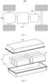
- FIG. 1 is a schematic structural diagram of the vehicle 1000 according to some embodiments of this application.
- the vehicle 1000 may be a fuel vehicle, a gas vehicle, or a new energy vehicle, where the new energy vehicle may be a battery electric vehicle, a hybrid electric vehicle, a range-extended vehicle, or the like.
- the vehicle 1000 is provided with a battery 100 inside, and the battery 100 may be disposed at the bottom, front, or rear of the vehicle 1000.
- the battery 100 may be configured to supply power to the vehicle 1000.
- the battery 100 may be used as an operational power source for the vehicle 1000.
- the vehicle 1000 may further include a controller 200 and a motor 300, where the controller 200 is configured to control the battery 100 to supply power to the motor 300, for example, to satisfy power needs of start, navigation, and driving of the vehicle 1000.
- the battery 100 can be used as not only the operational power source for the vehicle 1000 but also a driving power source for the vehicle 1000, replacing or partially replacing fossil fuel or natural gas to provide driving traction for the vehicle 1000.
- FIG. 2 is an exploded view of a battery 100 according to some embodiments of this application.
- the battery 100 includes a box 10 and a battery cell 20, where the battery cell 20 is accommodated in the box 10.
- the box 10 is configured to provide an accommodating space for the battery cell 20.
- the box 10 may be a variety of structures.
- the box 10 may include a first portion 11 and a second portion 12. The first portion 11 and the second portion 12 fit together so that the first portion 11 and the second portion 12 jointly define a space for accommodating the battery cell 20.
- the second portion 12 may be a hollow structure with one end open, and the first portion 11 may be a plate structure, where the first portion 11 covers the open side of the second portion 12 for the first portion 11 and the second portion 12 to jointly define an accommodating space.
- the first portion 11 and the second portion 12 may both be hollow structures with one side open, where the open side of the first portion 11 is engaged with the open side of the second portion 12.
- the box 10 formed by the first portion 11 and the second portion 12 may have a variety of shapes, for example, cylinder or cuboid.
- a plurality of battery cells 20 may be provided, and the plurality of battery cells 20 may be connected in series, parallel, or series-parallel, where being connected in series-parallel means a combination of series and parallel connections of the plurality of battery cells 20.
- the plurality of battery cells 20 may be directly connected in series, parallel, or series-parallel, and then an entirety of the plurality of battery cells 20 is accommodated in the box 10; or certainly, the battery 100 may be formed by a plurality of battery cells 20 connected in series, parallel, or series-parallel first to form a battery module and then a plurality of battery modules being connected in series, parallel, or series-parallel to form an entirety which is accommodated in the box 10.
- the battery 100 may further include other structures.
- the battery 100 may further include a busbar configured to implement electrical connection between the plurality of battery cells 20.
- Each battery cell 20 may be a secondary battery or a primary battery, and may be a lithium-sulfur battery, a sodium-ion battery, or a magnesium-ion battery, without being limited thereto.
- the battery cell 20 may be cylindrical, flat, cuboid, or of other shapes.
- FIG. 3 is a schematic structural exploded view of a battery cell 20 according to some embodiments of this application.
- the battery cell 20 refers to a smallest element constituting the battery 100.
- the battery cell 20 includes an end cover 21, a housing 22, an electrode assembly 23, and other functional components.
- the end cover 21 refers to a component that covers an opening of the housing 22 to separate an internal environment of the battery cell 20 from an external environment.
- a shape of the end cover 21 is not limited and may be adapted to a shape of the housing 22 to fit the housing 22.
- the end cover 21 may be made of a material with specified hardness and strength (for example, aluminum alloy), so that the end cover 21 is less likely to deform when subjected to extrusion and collision, allowing the battery cell 20 to have higher structural strength and enhanced reliability.
- the end cover 21 may be provided with functional components such as an electrode terminal 211.
- the electrode terminal 211 may be configured to be electrically connected to the electrode assembly 23 for outputting or inputting electrical energy of the battery cell 20.
- the end cover 21 may further be provided with a pressure relief mechanism for releasing internal pressure when the internal pressure or a temperature of the battery cell 20 reaches a threshold.
- the end cover 21 may also be made of various materials, such as copper, iron, aluminum, stainless steel, aluminum alloy, and plastic, which are not particularly limited in the embodiments of this application.
- an insulation part may also be provided at an inner side of the end cover 21.
- the insulation part may be configured to isolate an electrically connected component in the housing 22 from the end cover 21 to reduce a risk of short circuit.
- the insulation part may be made of plastic, rubber, or the like.
- the housing 22 is an assembly configured to form an internal environment of the battery cell 20 together with the end cover 21, where the formed internal environment may be configured to accommodate the electrode assembly 23, an electrolyte, and other components.
- the housing 22 and the end cover 21 may be separate components, an opening may be provided on the housing 22, and the end cover 21 covers the opening to form the internal environment of the battery cell 20.
- the end cover 21 and the housing 22 are not limited and may also be integrated. Specifically, the end cover 21 and the housing 22 may form a shared connection surface before other components are disposed inside the housing, and then the housing 22 is covered with the end cover 21 when inside of the housing 22 needs to be enclosed.
- the housing 22 may be of various shapes and sizes, such as a rectangular shape, a cylindrical shape, and a hexagonal prism shape.
- a shape of the housing 22 may be determined according to a specific shape and size of the electrode assembly 23.
- the housing 22 may be made of various materials, such as copper, iron, aluminum, stainless steel, aluminum alloy, and plastic, which are not particularly limited in the embodiments of this application.
- the electrode assembly 23 is a component in which electrochemical reactions occur in the battery cell 20.
- the housing 22 may include one or more electrode assemblies 23.
- the electrode assembly 23 is mainly formed by winding or stacking two electrode plates 231 with opposite polarities, and a separator is generally provided between the two electrode plates 231 with opposite polarities.
- the separator may be made of PP (polypropylene, polypropylene), PE (polyethylene, polyethylene), or the like.
- Portions of the two electrode plates 231 with opposite polarities that have an active substance constitutes a body portion of the electrode assembly 23, while portions of the two electrode plates 231 with opposite polarities that have no active substance separately constitute a tab 2312, which means that portions of the two electrode plates 231 with opposite polarities that have no active substance constitute a positive electrode tab and a negative electrode tab, respectively.
- a positive electrode tab and a negative electrode tab may both be located at one end of the body portion or be located at two ends of the body portion, respectively.
- the electrode plate 231 includes a current collector 2311 and an active substance layer 2313.
- the current collector 2311 includes a conductive layer 23111 and an insulating layer 23112, where in thickness direction Y of the electrode plate, the conductive layer 23111 is provided at two opposite sides of the insulating layer 23112;
- the insulating layer 23112 includes a first region 231121 and a second region 231122, thickness of the second region 231122 being less than thickness of the first region 231121, and in width direction X of the electrode plate, at least one end of the first region 231121 being connected to the second region 231122;
- the conductive layer 23111 includes a tab portion 231111, the tab portion 231111 being at least partially disposed in the second region 231122.
- the active substance layer 2313 is applied to a surface of the conductive layer 23111 facing away from the insulating layer 23112, the tab portion 231111 being not coated with the active substance layer 2313.
- the active substance layer 2313 is made of different materials based on the polarity of the electrode plate 231.
- the active substance layer 2313 may be lithium cobaltate, lithium iron phosphate, lithium ternary, lithium manganate, or the like.
- the active substance layer 2313 may be carbon, silicon, or the like.
- the current collector 2311 includes an insulating layer 23112 and two conductive layers 23111, and in thickness direction Y of the electrode plate, the two conductive layers 23111 are disposed at two sides of the insulating layer 23112, respectively.
- the conductive layers 23111 may be bonded to a surface of the insulating layer 23112 in the thickness direction Y of the electrode plate, or may be disposed on a side of the insulating layer 23112 in the thickness direction Y of the electrode plate using other connection methods, such as fusion bonding.
- materials for the conductive layer 23111 may be different. For example, if the electrode plate 231 is a positive electrode plate, the conductive layer 23111 may be made of aluminum, and if the electrode plate 231 is a negative electrode plate, the conductive layer 23111 may be made of copper.
- the material of the insulating layer 23112 includes at least one of polyethylene terephthalate or polypropylene.
- the first region 231121 and the second region 231122 are arranged along the width direction X of the electrode plate, and an end of the first region 231121 is connected to an end of the second region 231122.
- the first region 231121 and the second region 231122 may be directly or indirectly connected.
- the width direction X of the electrode plate is perpendicular to the thickness direction Y of the electrode plate.
- the first region 231121 may be an equal-thickness structure or a non-equal-thickness structure.
- the second region 231122 may be an equal-thickness structure or a non-equal-thickness structure.
- the thickness of the first region 231121 may be the smallest dimension of the first region 231121 in the thickness direction Y of the electrode plate, and the thickness of the second region 231122 may be the largest dimension of the second region 231122 in the thickness direction Y of the electrode plate.
- the smallest dimension of the first region 231121 in the thickness direction Y of the electrode plate is greater than the largest dimension of the second region 231122 in the thickness direction Y of the electrode plate.
- Each conductive layer 23111 has a tab portion 231111.
- the second region 231122 and the tab portions 231111, disposed in the second region 231122, of the two conductive layers 23111 together form the tabs 2312 of the electrode plate 231.
- the conductive layer 23111 may include a plurality of tab portions 231111 spaced apart in length direction Z of the electrode plate, and the insulating layer 23112 may include a plurality of second regions 231122 spaced apart in the length direction Z of the electrode plate, such that the electrode plate 231 may form a plurality of tabs 2312 spaced apart in the length direction Z of the electrode plate.
- the thickness direction Y of the electrode plate, the width direction X of the electrode plate, and the length direction Z of the electrode plate are perpendicular to each other.
- the plurality of tabs 2312 are stacked and welded.
- the plurality of tabs 2312 are stacked and welded so that the tab portions 231111 at two sides of each tab 2312 in the thickness direction Y of the electrode plate are communicated and electrically connected. It is possible to achieve communication between two tab portions 231111 at the tab 2312 by welding an adapter (not shown in the figure) at each tab, and then the adapters corresponding to the individual tabs 2312 are welded to establish electrical connections in the individual tabs 2312.
- the adapters may be electrically connected to the electrode terminals 211 on the end cover 21.
- the tab portions 231111 may be disposed in the second region 231122 in its entirety.
- a region at which the conductive layer 23111 overlaps the second region 231122 is the tab portion 231111.
- the tab portion 231111 may be partially disposed in the second region 231122.
- the tab portion 231111 of the conductive layer 23111 disposed in the second region 231122 with a smaller thickness when individual tab portions 231111 of the electrode assembly 23 formed using the electrode plate 231 are welded, the tab portions 231111 at the two sides of the second region 231122 are more easily welded due to the smaller thickness of the second region 231122, thereby achieving electrical connection between the two tab portions 231111, reducing welding difficulty, and mitigating the risk caused by welding quality issues such as false welding of the tab portions 231111 due to the presence of the insulating layer 23112, which is conducive to the improvement in the welding quality of the individual tab portions 231111 of the electrode assembly 23 having the electrode plate 231 and thereby the improvement in the reliability of the battery 100 or battery cell 20 having the electrode plate 231.
- the insulating layer 23112 further includes a first transition zone 231123, the first transition zone 231123 connecting the first region 231121 and the second region 231122, and thickness of the first transition zone 231123 gradually decreasing in a direction from the first region 231121 to the second region 231122.
- an end of the first transition zone 231123 is connected to the first region 231121, and another end of the first transition zone 231123 is connected to the second region 231122.
- the first region 231121 and the second region 231122 are indirectly connected through the first transition zone 231123.
- Two surfaces of the first transition zone 231123 in the thickness direction Y of the electrode plate may be curved surfaces or may be planar surfaces inclined from the first region 231121 to the second region 231122.
- the first region 231121, the second region 231122, and the first transition zone 231123 may be provided separately and connected together using a connection process such as bonding connection and fusion connection, to form the insulating layer 23112.
- the first region 231121, the second region 231122, and the first transition zone 231123 may alternatively be integrally formed. Materials of the first region 231121, the second region 231122, and the first transition zone 231123 may be the same or different.
- the thickness of the first transition zone 231123 gradually decreases.
- the first transition zone 231123 has a smaller thickness at a position closer to the second region 231122.
- the provision of the first transition zone 231123 can reduce the risk of forming stress concentration between the first region 231121 and the second region 231122, improving the fatigue life of the electrode plate 231 and reducing the risk of breakage of the electrode plate 231.
- a thickness difference can be formed at the connection position between the first region 231121 and the second region 231122, which means that the thickness of the end of the first region 231121 connected to the second region 231122 is greater than the thickness of the end of the second region 231122 connected to the first region 231121.
- the thickness of the end of the second region 231122 connected to the first region 231121 may alternatively be substantially the same as the thickness of the end of the first region 231121 connected to the second region 231122.
- the thickness of the second region 231122 gradually decreases, so that there is less risk of forming stress concentration under the condition that the first region 231121 and the second region 231122 are directly connected, which is conducive to improving the fatigue life of the electrode plate 231 and reducing the risk of breakage of the electrode plate 231.
- the conductive layer 23111 further includes a coating portion 231112, the coating portion 231112 being disposed in the first region 231121; at least a portion of the active substance layer 2313 is applied to a side of the coating portion 231112 facing away from the first region 231121; and thickness of the coating portion 231112 is less than thickness of the tab portion 231111.
- the coating portion 231112 and the tab portion 231111 are disposed in the width direction X of the electrode plate. An end of the coating portion 231112 is connected to an end of the tab portion 23 1111, and the coating portion 231112 and the tab portion 231111 are electrically connected. In this regard, the coating portion 231112 and the tab portion 231111 may be directly or indirectly connected.
- the coating portion 231112 is configured for application of an active substance layer 2313 (shown in FIG. 4 ).
- the active substance layer 2313 is applied to the side of the coating portion 231112 facing away from the first region 231121.
- the active substance layer 2313 applied to the side of the conductive layer 23111 facing away from the insulating layer 23112 may be entirely applied to the coating portion 231112, or a portion of the active substance layer 2313 applied to the side of the conductive layer 23111 facing away from the insulating layer 23112 may be applied to the coating portion 231112, and another portion thereof is applied beyond the coating portion 231112 in the width direction X of the electrode plate.
- the coating portion 231112 may be an equal-thickness structure or a non-equal-thickness structure.
- the tab portion 231111 may be an equal-thickness structure or a non-equal-thickness structure.
- the thickness of the coating portion 231112 may be the largest dimension of the coating portion 231112 in the thickness direction Y of the electrode plate, and the thickness of the tab portion 231111 may be the smallest dimension of the tab portion 231111 in the thickness direction Y of the electrode plate. In other words, the largest dimension of the coating portion 231112 in the thickness direction Y of the electrode plate is less than the smallest dimension of the tab portion 231111 in the thickness direction Y of the electrode plate.
- the thickness of the coating portion 231112 is less than the thickness of the tab portion 231111, which can compensate to a certain extent for the dimensional difference in which the thickness of the first region 231121 is greater than the thickness of the second region 231122. This reduces the thickness difference at various positions of the current collector 2311, which is conducive to improving the structural dimensional homogeneity of the current collector 2311 and thereby improving the quality of the electrode plate 231.
- the thickness of the coating portion 231112 may alternatively be the same as the thickness of the tab portion 231111, which facilitates the provision of the conductive layer 23111 on the insulating layer 23112 and thereby facilitates the manufacturing and molding of the current collector 2311.
- the conductive layer 23111 includes a coating portion 231112, the coating portion 231112 being disposed in the first region 231121; at least a portion of the active substance layer 2313 is applied to a side of the coating portion 231112 facing away from the first region 231121; and a surface of the coating portion 231112 facing away from the first region 231121 and a surface of the tab portion 231111 facing away from the second region 231122 are co-planar.
- the surface of the coating portion 231112 facing away from the first region 231121 is a first sub surface 231113, and the surface of the tab portion 231111 facing away from the second region 231122 is a second sub surface 231114.
- the surface of the coating portion 231112 facing away from the first region 231121 and the surface of the tab portion 231111 facing away from the second region 231122 are co-planar, which means that the first sub surface 231113 and the second sub surface 231114 are co-planar, or, in other words, the first sub surface 231113 and the second sub surface 231114 are located on a same plane.
- the thickness of the second region 231122 is greater than the thickness of the first region 231121 and the surface of the coating portion 231112 facing away from the first region 231121 and the surface of the tab portion 231111 facing away from the second region 231122 are co-planar, the thickness of the tab portion 231111 is greater than the thickness of the coating portion 231112, which is conducive to improving the current flow capability of the tab 2312 of the electrode plate 231.
- the surface of the coating portion 231112 facing away from the first region 231121 and the surface of the tab portion 231111 facing away from the second region 231122 are co-planar, so that the surface of the current collector 2311 in the thickness direction Y of the electrode plate is much flatter, facilitating the manufacturing and molding of the current collector 2311.
- the surface of the coating portion 231112 facing away from the first region 231121 and the surface of the tab portion 231111 facing away from the second region 231122 may alternatively not be co-planar.
- the thickness of the coating portion 231112 is the same as the thickness of the tab portion 231111
- the surface of the coating portion 231112 facing away from the first region 231121 and the surface of the tab portion 231111 facing away from the second region 231122 are not co-planar, and in the thickness direction Y of the electrode plate, a distance between the surface (first sub surface 231113) of the coating portion 231112 facing away from the first region 231121 and the surface of the first region 231121 facing the coating portion 231112 is greater than a distance between the surface (second sub surface 231114) of the tab portion 231111 facing away from the surface of the second region 231122 and the surface of the first region 231121 facing the coating portion 231112.
- the insulating layer 23112 further includes a first transition zone 231123, the first transition zone 231123 connecting the first region 231121 and the second region 231122, and thickness of the first transition zone 231123 gradually decreasing in a direction from the first region 231121 to the second region 231122; and the conductive layer 23111 further includes a second transition zone 231115, the second transition zone 231115 being disposed in the first transition zone 231123, and thickness of the second transition zone 231115 gradually increasing in the direction from the first region 231121 to the second region 231122.
- an end of the second transition zone 231115 is connected to the coating portion 231112, and another end of the first transition zone 231123 is connected to the tab portion 231111.
- the coating portion 231112 and the tab portion 231111 are indirectly connected through the first transition zone 231123.
- the coating portion 231112, the tab portion 231111, and the second transition zone 231115 may be provided separately and connected together using a connection process such as bonding connection and fusion connection, to form the conductive layer 23111.
- the coating portion 231112, the tab portion 231111, and the second transition zone 231115 may alternatively be integrally formed. Materials of the coating portion 231112, the tab portion 231111, and the second transition zone 231115 may be the same or different.
- the second transition zone 231115 may also be regarded as a part of the tab portion 231111, such that only a part of the tab portion 231111 is disposed in the second region 231122 and another part of the tab portion 231111 is disposed in the first transition zone 231123 of the insulating layer 23112.
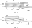
- the second transition zone 231115 may or may not be welded to the adapter 24 (shown in FIG. 11 ).
- the thickness of the second transition zone 231115 gradually increases.
- the second transition zone 231115 has a larger thickness at a position closer to the second region 231122.
- the thickness of the first transition zone 231123 gradually decreases and the thickness of the second transition zone 231115 gradually increases, which can compensate for the thickness difference of the first transition zone 231123 with respect to the first region 231121 and the second region 231122.
- a surface of the second transition zone 231115 facing away from the first transition zone 231123 and a surface of the tab portion 231111 facing away from the second region 231122 are co-planar.
- the surface of the second transition zone 231115 facing away from the first transition zone 231123 is a third sub surface 231126, and the surface of the second transition zone 231115 facing away from the first transition zone 231123 and the surface of the tab portion 231111 facing away from the second region 231122 are co-planar, which means that the third sub surface 231126 and the second sub surface 231114 are co-planar, or in other words, the third sub surface 231126 and the second sub surface 231114 are located on a same plane.
- the surface of the second transition zone 231115 facing away from the first transition zone 231123 and the surface of the tab portion 231111 facing away from the second region 231122 are co-planar, so that the surface of the current collector 2311 in the thickness direction Y of the electrode plate is much flatter, facilitating the manufacturing and molding of the current collector 2311.
- the surface of the second transition zone 231115 facing away from the first transition zone 231123 and the surface of the tab portion 231111 facing away from the second region 231122 are co-planar, and the surface of the coating portion 231112 facing away from the first region 231121 and the surface of the tab portion 231111 facing away from the second region 231122 may or may not be co-planar.
- two ends of the first region 231121 are connected to the second region 231122.
- the electrode plate 231 has tabs 2312 formed at two ends in its width direction.
- Two second regions 231122 are connected to two ends of the first region 231121 in the width direction X of the electrode plate, respectively.
- the two second regions 231122 may be connected to the first region 231121 in a same way.
- the two second regions 231122 are directly connected to the two ends of the first region 231121 in the width direction X of the electrode plate, respectively, or the two second regions 231122 are indirectly connected to the first region 231121 through the first transition zone 231123, respectively, which facilitates the manufacturing and molding of the current collector 2311.
- the two second regions 231122 may alternatively be connected to the first region 231121 in different ways.
- one of the two second regions 231122 is directly connected to an end of the first region 231121, and the other of the two second regions 231122 is indirectly connected to another end of the first region 231121 through the first transition zone 231123, which can form two tabs 2312 of different forms, enabling the electrode plate 231 to meet different usage requirements.
- the current collector 2311 can be cut in the middle to synchronously manufacture two electrode plates 231, which is conducive to improving the production efficiency of preparing the electrode plate 231.
- an end of the first region 231121 is connected to the second region 231122.
- the conductive layer 23111 has a first surface 231117 facing away from the insulating layer 23112, the first surface 231117 extending to two ends of the current collector 2311 along the width direction X of the electrode plate; and in the thickness direction Y of the electrode plate, the first surfaces 231117 of the conductive layers 23111 at the two opposite sides of the insulating layer 23112 are parallel.
- the first surface 231117 includes a first sub surface 231113 and a second sub surface 231114, the first sub surface 231113 and the second sub surface 231114 being co-planar.
- the conductive layer 23111 further includes a second transition zone 231115
- the first surface 231117 includes a first sub surface 231113, a second sub surface 231114, and a third sub surface 231126, the first sub surface 231113, the second sub surface 231114, and the third sub surface 231126 being co-planar and together forming the first surface 231117.
- an edge, facing away from the second sub surface 231114, of the first sub surface 231113 of the tab portion 231111 disposed in a second region 231122 forms an edge of the first surface 231117, and an edge, facing away from the second sub surface 231114, of the first sub surface 231113 of the tab portion 231111 disposed in another second region 231122 forms another edge of the first surface 231117.
- the second region 231122 is provided at only an end of the first region 231121, in the width direction X of the electrode plate, an edge, facing away from the second sub surface 23 1114, of the first sub surface 231113 forms an edge of the first surface 231117, and an edge, facing away from the first sub surface 231113, of the second sub surface 231114 forms another edge of the first surface 231117.
- the conductive layer 23111 has a first surface 231117 facing away from the insulating layer 23112, the first surface 231117 extending to two ends of the current collector 2311 along the width direction X of the electrode plate, which means that the first surface 231117 is planar, facilitating the manufacturing and molding and facilitating the application of the active substance layer 2313 on the first surface 231117, thereby facilitating the manufacturing and molding of the electrode plate 231.
- the first surfaces 231117 of the conductive layers 23111 at the two opposite sides of the insulating layer 23112 are parallel, and the current collector 2311 is an equal-thickness structure, facilitating the manufacturing and molding of the current collector 2311.
- the conductive layer 23111 further includes a coating portion 231112, the coating portion 231112 being disposed in the first region 231121, and in the thickness direction Y of the electrode plate, an active substance layer 2313 is provided on a side of the coating portion 231112, facing away from the insulating layer 23112, of the conductive layer 23111 at two sides of the insulating layer 23112.
- the active substance layer 2313 is applied to the surface of the coating portion 231112 facing away from the first region 231121, which means that the active substance layer 2313 is applied to the first sub surface 231113. It is possible that the coating portions 231112 of two conductive layers 23111 are provided with the active substance layer 2313.
- the active substance layer 2313 is provided on a side of the coating portion 231112, facing away from the insulating layer, of the conductive layer 23111 at the two sides of the insulating layer 23112, which increases the amount of active substance of the electrode plate 231 and is conducive to increasing the energy density of the battery 100 or battery cell 20 having the electrode plate 231.
- the active substance layer 2313 can alternatively be applied at the coating portion 231112 of only one conductive layer 23111.
- a projection of the active substance layer 2313 and a projection of the second region 231122 do not overlap when viewed from the thickness direction Y of the electrode plate.
- the projection of the active substance layer 2313 refers to a projection of the active substance layer 2313 on a plane perpendicular to the thickness direction Y of the electrode plate.
- the projection of the second region 231122 refers to a projection of the second region 231122 on a plane perpendicular to the thickness direction Y of the electrode plate.
- the active substance layer 2313 is entirely applied to the coating portion 231112 of the conductive layer 23111, so that when the tab portion 231111 is welded, in the width direction X of the electrode plate, a spacing can be formed between a welding location and the active substance layer 2313, which can mitigate the risk of high-temperature damage to the active substance layer 2313 during welding.
- a portion of the active substance layer 2313 is applied to the coating portion 231112 of the conductive layer 23111, and that another portion thereof extending along the width direction X of the electrode plate to the conductive layer 23111 is applied in the second region 231122.
- the conductive layer 23111 includes a second transition zone 231115, and in the width direction X of the electrode plate, the active substance layer 2313 covers the first transition zone 231123 and extends to overlap the second region 231122.
- thickness H 1 of the second region 231122 and thickness L 1 of the tab portion 231111 satisfy H 1 /L 1 ⁇ 5.
- H 1 /L 1 may be 0.5, 1, 1.5, 2, 2.5, 3, 3.5, 4, 4.5, 5, or the like.
- H 1 /L 1 > 5 an area of welding residue during welding of individual tab portions 231111 is relatively small, resulting in relatively poor welding stability and less likelihood of false welding. Therefore, H 1 /L 1 ⁇ 5, so that a relatively large area of welding residue can be left between two tab portions 231111 after tab portions 231111 at two sides of the second region 231122 are welded, which makes the welding more stable and reduces the risk of welding quality issues such as false welding.
- the area of welding residue refers to a proportion of the area of residue in welding of the adapter in an entire welding area after the welding is completed.
- the area of welding residue on the adapter may be manually and visually inspected after the welding tension was measured using a tension, where the welding tension can be greater than or equal to 100 N.
- the area of welding residue is required to be greater than or equal to 50% to meet the basic requirements of use, but in actual production, the area of welding residue needs to be greater than or equal to 80% to meet the acceptance criteria. Data in Table 1 is obtained.
- H 1 /L 1 when H 1 /L 1 is 5.2, 5.5, 5.7, and 5, the area of welding residue is less than 50%, so the battery cells 20 produced cannot meet the basic requirements of use.
- H 1 /L 1 is 0.1, 0.2, 0.5, 0.7, 0.9, 0.2, 1, 1.2, 1.5, 1.7, 1.9, 2, 2.2, 2.5, 2.7, 3, 3.2, 3.5, 3.7, 3.9, 4, 4.2, 4.5, 4.7, and 4.9, the area of welding residue is greater than 50%, so the battery cells 20 produced can meet the basic requirements of use.
- H 1 /L 1 ⁇ 5 so that a relatively large area of welding residue can be left between two tab portions 231111 after tab portions 231111 at two sides of the second region 231122 are welded, which makes the welding more stable and reduces the risk of welding quality issues such as false welding, so that the battery cells 20 meet the requirements of use.
- H 1 /L 1 when H 1 /L 1 is 1.2, 1.5, 1.7, 1.9, 2, 2.2, 2.5, 2.7, 3, 3.2, 3.5, 3.7, 3.9, 4, 4.2, 4.5, 4.7, and 4.9, the area of welding residue, although also relatively large, still falls below the actual production acceptance criteria.
- H 1 /L 1 is 0.1, 0.2, 0.5, 0.7, 0.9, 0.2, and 1, the area of welding residue reaches 80% or more, meeting the actual production acceptance criteria.
- H 1 /L 1 may be 0.1, 0.2, 0.3, 0.4, 0.5, 0.6, 0.7, 0.8, 0.9, 1, or the like.
- the thickness H 1 of the second region 231122 may have different values according to actual requirements. In some embodiments, H 1 ⁇ 15 ⁇ m. For example, H 1 may be 1 ⁇ m, 3 ⁇ m, 5 ⁇ m, 7 ⁇ m, 9 ⁇ m, 11 ⁇ m, 13 ⁇ m, 15 ⁇ m, or the like.
- the thickness of the second region 231122 is large, which is not conducive to the welding of the two tab portions 231111 at two sides of the second region 231122, and furthermore, the thickness of the first region 231121 is greater than the thickness of the second region 231122. If H 1 > 15 ⁇ m, the thicknesses of both the second region 231122 and the first region 231121 are large, resulting in a large overall thickness of the current collector 2311, which is not conducive for a cell with the electrode plate 231 prepared using the current collector 2311 and the electrode assembly 23 thus formed to have high energy density. Therefore, if H 1 ⁇ 15 ⁇ m, a reduced thickness of the current collector 2311 is conducive for the cell with the electrode plate 231 prepared using the current collector 2311 and the electrode assembly 23 thus formed to have high energy density.
- H 1 ⁇ 5 ⁇ m.
- H 1 may be 0.5 ⁇ m, 1.5 ⁇ m, 2 ⁇ m, 2.5 ⁇ m, 4 ⁇ m, 4.5 ⁇ m, 5 ⁇ m, or the like.
- the thickness L 1 of the tab portion 231111 may have different values according to actual requirements. In some embodiments, 0.1 ⁇ m ⁇ L 1 ⁇ 10 ⁇ m.
- L 1 may be 0.1 ⁇ m, 1 ⁇ m, 2 ⁇ m, 3 ⁇ m, 4 ⁇ m, 5 ⁇ m, 6 ⁇ m, 7 ⁇ m, 8 ⁇ m, 9 ⁇ m, 10 ⁇ m, or the like.
- the tab portion 231111 may not satisfy the current flow demand, and if L 1 > 10 ⁇ m, the tab portion 231111 has a larger thickness, making the current collector 2311 thicker. 0.1 ⁇ m ⁇ L 1 ⁇ 10 ⁇ m, so that the tab portion 231111 can have a better current flow capability and the thickness of the current collector 2311 is controlled in a reasonable range.
- L 1 may be 2 ⁇ m, 2.2 ⁇ m, 2.5 ⁇ m, 2.7 ⁇ m, 3.2 ⁇ m, 3.5 ⁇ m, 3.7 ⁇ m, 3.9 ⁇ m, 4 ⁇ m, or the like.
- the conductive layer 23111 further includes a coating portion 231112, the coating portion 231112 being disposed in a first region 231121, and thickness H 2 of the first region 231121 and thickness L 2 of the coating portion 231112 satisfy 1 ⁇ H 2 /L 2 ⁇ 50.
- the first region 231121 is an equal-thickness structure, and the thickness of the first region 231121 is a dimension of the first region 231121 in the thickness direction Y of the electrode plate.
- the coating portion 231112 is an equal-thickness structure, and the thickness of the coating portion 231112 is a dimension of the tab portion 231111 in the thickness direction Y of the electrode plate.
- H 2 /L 2 may be 1, 5, 10, 15, 20, 25, 30, 35, 40, 45, 50, or the like.
- H 2 /L 2 ⁇ 1 under the condition that the thickness of the current collector 2311 is constant, the thickness of the first region 231121 is smaller with respect to the thickness of the coating portion 231112, which makes the portion of the current collector 2311 including the first region 231121 have a weak strength. If H 2 /L 2 > 50, the thickness of the coating portion 231112 is smaller with respect to the thickness of the first region 231121, and it is difficult to make the conductive layer 23111 have a high current flow capability under the condition that the thickness of the current collector 2311 is constant. Therefore, 1 ⁇ H 2 /L 2 ⁇ 50, so that the current collector 2311 has a good strength and the conductive layer 23111 has a good current flow capability.
- H 2 /L 2 may be 2, 3, 4, 6, 7, 9, 11, 13, 16, 17, 18, 19, 20, or the like.
- the thickness H 2 of the first region 231121 may have different values according to actual requirements. In some embodiments, 1 ⁇ m ⁇ H 2 ⁇ 20 ⁇ m. For example, Hz may be 1 ⁇ m, 2 ⁇ m, 3 ⁇ m, 5 ⁇ m, 6 ⁇ m, 9 ⁇ m, 10 ⁇ m, 13 ⁇ m, 15 ⁇ m, 17 ⁇ m, 20 ⁇ m, or the like.
- the first region 231121 has a low strength, and if H 2 > 20 ⁇ m, the first region 231121 has a larger thickness, making the current collector 2311 thicker. 1 ⁇ m ⁇ H 2 ⁇ 20 ⁇ m, so that the first region 231121 has a better strength and the thickness of the current collector 2311 is controlled in a reasonable range.
- Hz may be 3 ⁇ m, 4 ⁇ m, 7 ⁇ m, 8 ⁇ m, 11 ⁇ m, 11.5 ⁇ m, 12 ⁇ m, 13.5 ⁇ m, 14 ⁇ m, or the like.
- the thickness L 2 of the coating portion 231112 may have different values according to actual requirements. In some embodiments, 0.1 ⁇ m ⁇ L 2 ⁇ 10 ⁇ m.
- L 2 may be 0.1 ⁇ m, 1 ⁇ m, 2 ⁇ m, 3 ⁇ m, 4 ⁇ m, 5 ⁇ m, 6 ⁇ m, 7 ⁇ m, 8 ⁇ m, 9 ⁇ m, 10 ⁇ m, or the like.
- the coating portion 231112 has a small current flow capability and may not meet the requirements of use, and if L 2 > 10 ⁇ m, the coating portion 231112 has a larger thickness, making the current collector 2311 thicker. 0.1 ⁇ m ⁇ L 2 ⁇ 20 ⁇ m, so that the coating portion 231112 has a better current flow capability and the thickness of the current collector 2311 is controlled in a reasonable range.
- L 2 may be 0.5 ⁇ m, 1.5 ⁇ m, 2.5 ⁇ m, 3.5 ⁇ m, 4.5 ⁇ m, 5 ⁇ m, or the like.
- An embodiment of this application further provides an electrode assembly 23, the electrode assembly 23 including the electrode plate 231 provided in any one of the foregoing embodiments.
- the electrode assembly 23 includes two electrode plates 231 with opposite polarities, and the electrode plate 231 provided in any one of the foregoing embodiments may be a positive electrode plate or a negative electrode plate of the electrode assembly 23. It is also possible that the two electrode plates 231 with opposite polarities use the electrode plates 231 provided in any one of the foregoing embodiments.
- the tab portions 231111 at the two sides of the second region 231122 are more easily welded due to the smaller thickness of the second region 231122 of the insulating layer 23112 of the electrode plate 231 provided in any one of the foregoing embodiments, thereby reducing welding difficulty, and mitigating the risk caused by welding quality issues such as false welding of the tab portions 231111 due to the presence of the insulating layer 23112, which is conducive to the improvement in the welding quality of the individual tab portions 231111 of the electrode assembly 23 having the electrode plate 231.
- the electrode assembly 23 includes two electrode plates 231 according to any one of the foregoing embodiments with the two electrode plates 231 having opposite polarities.
- both the positive electrode plate and the negative electrode plate of the electrode assembly 23 use the plates 231 provided in any of the foregoing embodiments.
- the tab portions 231111 at the two sides of the second region 231122 are more easily welded due to the smaller thickness of the second region 231122 of the insulating layer 23112 of the electrode plate 231 provided in any one of the foregoing embodiments, thereby reducing welding difficulty, and mitigating the risk caused by welding quality issues such as false welding of the tab portions 231111 due to the presence of the insulating layer 23112.
- the two electrode plates 231 of the electrode assembly 23 with opposite polarities are both the electrode plates 231 provided in any one of the foregoing embodiments, so that the individual tab portions 231111 of the electrode assembly 23 establish a relatively stable electrical connection with one another.
- An embodiment of this application further provides a battery cell 20, the battery cell 20 including the electrode assembly 23 provided in any one of the foregoing embodiments.
- the welding of the tab portions 231111 of the electrode assembly 23 provided in any one of the foregoing embodiments can establish a stable electrical connection, thereby facilitating stable charging and discharging of the battery cell 20 and improving the reliability of the battery cell 20.
- the battery cell 20 further includes an adapter 24, where in the thickness direction Y of the electrode plate, the tab portions 231111 of the conductive layer 23111 located at two sides of the second region 231122 are welded to the adapter 24.
- the adapter 24 is disposed on a side of the tab portion 231111 facing away from the second region 231122. After the adapter 24 is welded to the tab portion 231111, the tab portions 231111 of the conductive layer 23111 disposed at two sides of the second region 231122 are electrically connected, and electrodes corresponding to the tab portions 231111 are led out through the adapter 24.
- Each tab 2312 may be correspondingly provided with an adapter 24. After the adapter 24 is welded to the corresponding tab 2312, the tab portions 231111 of that tab 2312 at two sides of the second region 231122 are electrically connected. The adapters 24 corresponding to the individual tab 2312 are then welded, thereby establishing electrical connections in the individual tabs 2312 to lead out of the electrodes.
- the adapter 24 may have various structural forms. As shown in FIG. 11 , in some embodiments, the adapter 24 includes a first sub adapter 241 and a second sub adapter 242.
- the first sub adapter 241 is located at a side of the tab portion 231111 of one of the two conductive layers 23111 facing away from the insulating layer 23112 and is welded to that tab portion 231111
- the second sub adapter 242 is located at a side of the tab portion 231111 of the other of the two conductive layers 23111 facing away from the insulating layer 23112 and is welded to that tab portion 231111.
- the length of the first sub adapter 241 is less than the length of the second sub adapter 242.
- the two tab portions 231111 are electrically connected, which is conducive to improving the current flow capability.
- the adapter 24 may alternatively be only a portion.
- the adapter 24 includes only the first sub adapter 241 or the second sub adapter 242.
- an end of the adapter 24 closest to the active substance layer 2313 may abut against the active substance layer 2313, so that a larger welding area is provided when the adapter 24 is welded to the tab portion 231111, thereby improving welding stability.
- a gap may alternatively be formed between the active substance layer 2313 and the end of the adapter 24 closest to the active substance layer 2313, to reduce the risk of high-temperature damage to the active substance layer 2313 during welding.
- the tab portions 231111 of the conductive layer 23111 located at the two sides of the second region 231122 are welded to the adapter 24, thereby achieving electrical connection between the tab portions 231111 at the two sides of the second region 231122. It can be understood that the tab portions 231111 at the two sides of the second region 231122 are all electrically connected to the adapter, and the electrodes of the battery cell 20 are led out through the adapter 24, which facilitates charging and discharging of the battery cell 20.
- An embodiment of this application further provides a battery 100, the battery 100 including the battery cell 20 provided in any one of the foregoing embodiments.
- the battery 100 may include one or more battery cells 20.
- the plurality of battery cells 20 are electrically connected to each other, and the plurality of battery cells 20 may be connected in series, parallel, or series-parallel.
- the welding of the tab portions 231111 of the electrode assembly 23 of the battery cell 20 provided in any one of the foregoing embodiments can establish a stable electrical connection, thereby facilitating stable charging and discharging of the battery cell 20 and improving the reliability of the battery 100 having the battery cell 20.
- An embodiment of this application further provides an electric device, the electric device including the battery cell 100 provided in any one of the foregoing embodiments.
- the battery 100 provided in the foregoing embodiments has better reliability, which is conducive to improving the reliability of power consumption of the electric device powered by the battery 100.
- An embodiment of this application provides an electrode plate 231, the electrode plate 231 including a current collector 2311 and an active substance layer 2313.
- the current collector 2311 includes an insulating layer 23112 and two conductive layers 23111. In thickness direction Y of the electrode plate, the two conductive layers 23111 are disposed at two sides of the insulating layer 23112, respectively.
- the insulating layer 23112 includes a first region 231121, a second region 231122, and a first transition zone 231123. In width direction X of the electrode plate, two ends of the first transition zone 231123 are connected to the first region 231121 and the second region 231122, respectively, and the second region 231122 is provided at one side of the first region 231121.
- the first region 231121 is an equal-thickness structure
- the second region 231122 is an equal-thickness structure
- thickness of the first region 231121 is greater than thickness of the second region 231122.
- the thickness of the first transition zone 231123 gradually decreases in a direction from the first region 231121 to the second region 231122.
- the conductive layer 23111 includes a tab portion 231111, a coating portion 231112, and a second transition zone 231115. In width direction X of the electrode plate, two ends of the second transition zone 231115 are connected to the tab portion 231111 and the coating portion 231112, respectively.
- the coating portion 231112 is disposed in the first region 231121
- the tab portion 231111 is disposed in the second region 231122
- the second transition zone 231115 is disposed in the first transition zone 231123.
- the coating portion 231112 is an equal-thickness structure
- the tab portion 231111 is an equal-thickness structure
- the thickness of the tab portion 231111 is greater than the thickness of the coating portion 231112.
- the thickness of the second transition zone 231115 gradually increases in a direction from the first region 231121 to the second region 231122.
- the electrode plate 231 is an equal-thickness structure.
- the first sub surface 231113 of the coating portion 231112 of each conductive layer 23111 facing away from the first region 231121, the second sub surface 231114 of the tab portion 231111 facing away from the second region 231122, and the third sub surface 231126 of the second transition zone 231115 facing away from the first transition zone 231123 are co-planar and together form the first surface 231117 of the current collector 2311 in the thickness direction Y of the electrode plate.
- the active substance layer 2313 is disposed on a side of the coating portion 231112 facing away from the first region 231121.
Landscapes
- Chemical & Material Sciences (AREA)
- Chemical Kinetics & Catalysis (AREA)
- Electrochemistry (AREA)
- General Chemical & Material Sciences (AREA)
- Engineering & Computer Science (AREA)
- Materials Engineering (AREA)
- Composite Materials (AREA)
- Connection Of Batteries Or Terminals (AREA)
Abstract
Description
- This application claims priority to
Chinese Patent Application No. 2023104453480, filed on April 24, 2023 - This application relates to the field of battery technologies, and specifically to an electrode plate, an electrode assembly, a battery cell, a battery, and an electric device.
- Batteries are widely used in portable electronic devices, electric transportation vehicles, electric tools, drones, energy storage devices, and other fields.
- The battery includes an electrode assembly, and tabs of the electrode assembly result in poor reliability of the battery due to poor welding quality.
- Embodiments of this application provide an electrode plate, an electrode assembly, a battery cell, a battery, and an electric device, so as to improve welding quality of tabs of the battery, thereby improving reliability of the battery.
- According to a first aspect, an embodiment of this application provides an electrode plate including a current collector and an active substance layer. The current collector includes a conductive layer and an insulating layer, where in thickness direction of the electrode plate, the conductive layer is provided at two opposite sides of the insulating layer. The insulating layer includes a first region and a second region, thickness of the second region being less than thickness of the first region, and in width direction of the electrode plate, at least one end of the first region being connected to the second region. The conductive layer includes a tab portion, the tab portion being at least partially disposed in the second region. The active substance layer is applied to a surface of the conductive layer facing away from the insulating layer, the tab portion being not coated with the active substance layer.
- In the foregoing technical solution, with the tab portion of the conductive layer disposed in the second region with a smaller thickness, when individual tab portions of the electrode assembly formed using the electrode plate are welded, the tab portions at the two sides of the second region are more easily welded due to the smaller thickness of the second region, thereby achieving electrical connection between the two tab portions, reducing welding difficulty, and mitigating the risk caused by welding quality issues such as false welding of the tab portions due to the presence of the insulating layer, which is conducive to the improvement in the welding quality of the individual tab portions of the electrode assembly having the electrode plate and thereby the improvement in the reliability of the battery or battery cell having the electrode plate.
- In some embodiments of the first aspect of this application, the insulating layer further includes a first transition zone, the first transition zone connecting the first region and the second region, and thickness of the first transition zone gradually decreasing in a direction from the first region to the second region.
- In the foregoing technical solution, the provision of the first transition zone can reduce the risk of forming stress concentration between the first region and the second region, improving the fatigue life of the electrode plate and reducing the risk of breakage of the electrode plate.
- In some embodiments of the first aspect of this application, the conductive layer further includes a coating portion, the coating portion being disposed in the first region; at least a portion of the active substance layer is applied to a side of the coating portion facing away from the first region; and thickness of the coating portion is less than thickness of the tab portion.
- In the foregoing technical solution, the thickness of the coating portion is less than the thickness of the tab portion, which can compensate to a certain extent for the dimensional difference in which the thickness of the first region is greater than the thickness of the second region. This reduces the thickness difference at various positions of the current collector, which is conducive to improving the structural dimensional homogeneity of the current collector and thereby improving the quality of the electrode plate.
- In some embodiments of the first aspect of this application, the conductive layer includes a coating portion, the coating portion being disposed in the first region; at least a portion of the active substance layer is applied to a side of the coating portion facing away from the first region; and a surface of the coating portion facing away from the first region and a surface of the tab portion facing away from the second region are co-planar.
- In the foregoing technical solution, the surface of the coating portion facing away from the first region and the surface of the tab portion facing away from the second region are co-planar, so that the surface of the current collector in the thickness direction of the electrode plate is much flatter, facilitating the manufacturing and molding of the current collector.
- In some embodiments of the first aspect of this application, the insulating layer further includes a first transition zone, the first transition zone connecting the first region and the second region, and thickness of the first transition zone gradually decreasing in a direction from the first region to the second region; and the conductive layer further includes a second transition zone, the second transition zone being disposed in the first transition zone, and thickness of the second transition zone gradually increasing in the direction from the first region to the second region.
- In the foregoing technical solution, in the direction from the first region to the second region, the thickness of the first transition zone gradually decreases and the thickness of the second transition zone gradually increases, which can compensate for the thickness difference of the first transition zone with respect to the first region and the second region. This reduces the thickness difference at various positions of the current collector, which is conducive to improving the structural dimensional homogeneity of the current collector and thereby improving the quality of the electrode plate.
- In some embodiments of the first aspect of this application, a surface of the second transition zone facing away from the first transition zone and a surface of the tab portion facing away from the second region are co-planar.
- In the foregoing technical solution, the surface of the second transition zone facing away from the first transition zone and the surface of the tab portion facing away from the second region are co-planar, so that the surface of the current collector in the thickness direction of the electrode plate is much flatter, facilitating the manufacturing and molding of the current collector.
- In some embodiments of the first aspect of this application, in the width direction of the electrode plate, two ends of the first region are connected to the second region.
- In the foregoing technical solution, in the width direction of the electrode plate, two ends of the first region are connected to the second region, so that in manufacturing of the electrode plate, the current collector can be cut in the middle to synchronously manufacture two electrode plates, which is conducive to improving the production efficiency of preparing the electrode plate.
- In some embodiments of the first aspect of this application, the conductive layer has a first surface facing away from the insulating layer, the first surface extending to two ends of the current collector along the width direction of the electrode plate; and in the thickness direction of the electrode plate, the first surfaces of the conductive layers at the two opposite sides of the insulating layer are parallel.
- In the foregoing technical solution, the conductive layer has a first surface facing away from the insulating layer, the first surface extending to two ends of the current collector along the width direction of the electrode plate, which means that the first surface is planar, facilitating the manufacturing and molding and facilitating the application of the active substance layer on the first surface, thereby facilitating the manufacturing and molding of the electrode plate. The first surfaces of the conductive layers at the two opposite sides of the insulating layer are parallel, and the current collector is an equal-thickness structure, facilitating the manufacturing and molding of the current collector.
- In some embodiments of the first aspect of this application, the conductive layer further includes a coating portion, the coating portion being disposed in the first region, and in the thickness direction of the electrode plate, the active substance layer is provided on a side of the coating portion, facing away from the insulating layer, of the conductive layer at the two sides of the insulating layer.
- In the foregoing technical solution, the active substance layer is provided on a side of the coating portion, facing away from the insulating layer, of the conductive layer at the two sides of the insulating layer, which increases the amount of active substance of the electrode plate and is conducive to increasing the energy density of the battery or battery cell having the electrode plate.
- In some embodiments of the first aspect of this application, when viewed from the thickness direction of the electrode plate, a projection of the active substance layer overlaps a projection of the second region.
- In the foregoing technical solution, the projection of the active substance layer overlaps the projection of the second region in the thickness direction of the electrode plate, and in the width direction of the electrode plate, the active substance layer covers as much of the conductive layer as possible, which increases the amount of the active substance layer of the electrode plate and is conducive to increasing the energy density of the battery or battery cell.
- In some embodiments of the first aspect of this application, thickness H1 of the second region and thickness L1 of the tab portion satisfy H1/L1 ≤ 5.
- In the foregoing technical solution, if H1/L1 > 5, an area of welding residue during welding of individual tab portions is relatively small, resulting in relatively poor welding stability and a less likelihood of false welding. Therefore, H1/L1 ≤ 5, so that a relatively large area of welding residue can be left between two tab portions after tab portions at the two sides of the second region are welded, which makes the welding more stable and reduces the risk of welding quality issues such as false welding.
- In some embodiments of the first aspect of this application, H1/L1 ≤ 1.
- In the foregoing technical solution, H1/L1 ≤ 1, so that a larger area of welding residue is present after tab portions are welded, which further enhances the welding stability and further reduces the risk of welding quality issues such as false welding.
- In some embodiments of the first aspect of this application, the conductive layer further includes a coating portion, the coating portion being disposed in the first region, and thickness H2 of the first region and thickness L2 of the coating portion satisfy 1 ≤ H2/L2 ≤ 50.
- In the foregoing technical solution, if H2/L2 < 1, under the condition that the thickness of the current collector is constant, the thickness of the first region is smaller with respect to the thickness of the coating portion, which makes the portion of the current collector including the first region have a weak strength. If H2/L2 > 50, the thickness of the coating portion is smaller with respect to the thickness of the first region, and it is difficult to make the conductive layer have a high current flow capability under the condition that the thickness of the current collector is constant. Therefore, 1 ≤ H2/L2 ≤ 50, so that the current collector has a good strength and the conductive layer has a good current flow capability.
- In some embodiments of the first aspect of this application, 2 ≤ H2/L2 ≤ 20.
- In the foregoing technical solution, 2 ≤ H2/L2 ≤ 20, so that the current collector has a better strength and the conductive layer has a better current flow capability.
- According to a second aspect, an embodiment of this application provides an electrode assembly, the electrode assembly including the electrode plate according to any one of the embodiments of the first aspect.
- In the foregoing technical solution, the tab portions at the two sides of the second region are more easily welded due to the smaller thickness of the second region of the insulating layer of the electrode plate provided in the embodiments of the first aspect, thereby reducing welding difficulty, and mitigating the risk caused by welding quality issues such as false welding of the tab portions due to the presence of the insulating layer, which is conducive to the improvement in the welding quality of the individual tab portions of the electrode assembly having the electrode plate.
- In some embodiments of the second aspect of this application, the electrode assembly includes two electrode plates according to any one of the embodiments of the first aspect, with polarities of the two electrode plates being opposite.
- In the foregoing technical solution, the tab portions at the two sides of the second region are more easily welded due to the smaller thickness of the second region of the insulating layer of the electrode plate provided in the embodiments of the first aspect, thereby reducing welding difficulty, and mitigating the risk caused by welding quality issues such as false welding of the tab portions due to the presence of the insulating layer. The two electrode plates of the electrode assembly with opposite polarities are both the electrode plates according to any one of the embodiments of the first aspect, so that the individual tab portions of the electrode assembly establish a relatively stable electrical connection with one another.
- According to a third aspect, an embodiment of this application provides a battery cell, the battery cell including the electrode assembly according to any one of the embodiments of the second aspect.
- In the foregoing technical solution, the welding of the tab portions of the electrode assembly can establish a stable electrical connection, thereby facilitating stable charging and discharging of the battery cell and improving the reliability of the battery cell.
- In some embodiments of the third aspect, the battery cell further includes an adapter, and in thickness direction of the electrode plate, the tab portions of the conductive layer located at two sides of the second region are welded to the adapter.
- In the foregoing technical solution, the tab portions of the conductive layer located at the two sides of the second region are welded to the adapter, thereby achieving electrical connection between the tab portions at the two sides of the second region. It can be understood that the tab portions at the two sides of the second region are all electrically connected to the adapter, and electrodes of the battery cell are led out through the adapter, which facilitates charging and discharging of the battery cell.
- According to a fourth aspect, an embodiment of this application provides a battery, the battery including the battery cell according to any one of the embodiments of the third aspect.
- In the foregoing technical solution, the welding of the tab portions of the electrode assembly of the battery cell according to the embodiment of the second aspect can establish a stable electrical connection, thereby facilitating stable charging and discharging of the battery cell and improving the reliability of the battery having the battery cell.
- According to a fifth aspect, an embodiment of this application provides an electric device, the electric device including the battery according to the embodiment of the fourth aspect.
- In the foregoing technical solution, the battery according to the embodiment of the fourth aspect has better reliability, which is conducive to improving the reliability of power consumption of the electric device powered by the battery.
- To describe the technical solutions of the embodiments of this application more clearly, the following briefly describes the accompanying drawings required for describing the embodiments. It is appreciated that the accompanying drawings below show merely some embodiments of this application and thus should not be considered as limitations on the scope. Persons of ordinary skill in the art may still derive other related drawings from the accompanying drawings without creative efforts.
-
FIG. 1 is a schematic structural diagram of a vehicle according to some embodiments of this application; -
FIG. 2 is an exploded view of a battery according to some embodiments of this application; -
FIG. 3 is a schematic structural exploded view of a battery cell according to some embodiments of this application; -
FIG. 4 is a schematic structural diagram of an electrode plate according to some embodiments of this application; -
FIG. 5 is a schematic structural diagram of a current collector of an electrode plate according to some embodiments of this application; -
FIG. 6 is a schematic structural diagram of a current collector of an electrode plate according to some other embodiments of this application; -
FIG. 7 is a schematic structural diagram of a current collector of an electrode plate according to yet some other embodiments of this application; -
FIG. 8 is a schematic structural diagram of an electrode plate according to some other embodiments of this application; -
FIG. 9 is a schematic structural diagram of a current collector of the electrode plate inFIG. 8 ; -
FIG. 10 is a schematic structural diagram of an electrode plate according to yet some other embodiments of this application; -
FIG. 11 is a schematic diagram of connection between a tab and an adapter according to some embodiments of this application; and -
FIG. 12 is a schematic diagram of connection between a tab and an adapter according to some other embodiments of this application. - Reference signs: 1000. vehicle; 100. battery; 10. box; 11. first portion; 12. second portion; 20. battery cell; 21. end cover; 211. electrode terminal; 22. housing; 23. electrode assembly; 231. electrode plate; 2311. current collector; 23111. conductive layer; 231111. tab portion; 231112. coating portion; 231113. first sub surface; 231114. second sub surface; 231115. second transition zone; 231126. third sub surface; 231117. first surface; 23112. insulating layer; 231121. first region; 231122. second region; 231123. first transition zone; 2312. tab; 2313. active substance layer; 24. adapter; 241. first sub adapter; 242. second sub adapter; 200. controller; 300. motor; X. width direction of an electrode plate; Y thickness direction of an electrode plate; and Z. length direction of an electrode plate.
- To make the objectives, technical solutions, and advantages of the embodiments of this application clearer, the following clearly and completely describes the technical solutions in the embodiments of this application with reference to the accompanying drawings in the embodiments of this application. Apparently, the described embodiments are some but not all embodiments of this application. Generally, the components of the embodiments of this application as described and illustrated in the accompanying drawings herein can be arranged and designed in a variety of configurations.
- Therefore, the following detailed description of the embodiments of this application as provided in the accompanying drawings is not intended to limit the scope of this application but merely to represent selected embodiments of this application. All other embodiments obtained by persons of ordinary skill in the art based on the embodiments of this application without creative efforts shall fall within the protection scope of this application.
- It should be noted that, without conflict, the embodiments and features in the embodiments in this application may be combined with each other.
- It should be noted that similar reference numerals and letters indicate similar items in the following drawings, and therefore once an item is defined in one drawing, it does not need to be further defined or explained in the subsequent drawings.
- Currently, from a perspective of the market development, application of traction batteries is being more extensive. Traction batteries have been not only used in energy storage power supply systems such as hydroelectric power plants, thermal power plants, wind power plants, and solar power plants, but also widely used in many other fields including electric transportation tools such as electric bicycles, electric motorcycles, and electric vehicles, military equipment, and aerospace. With continuous expansion of application fields of traction batteries, market demands for the traction batteries are also expanding.
- The battery mentioned in the embodiments of this application is a single physical module that includes one or more battery cells for providing a higher voltage and capacity. For example, the battery mentioned in this application may include a battery module, a battery pack, or the like. A battery typically includes a box configured to enclose one or more battery cells. The box can prevent liquids or other foreign matter from affecting charging or discharging of the battery cell.
- In this application, the battery cell may include a lithium-ion secondary battery, a lithium-ion primary battery, a lithium-sulfur battery, a sodium-lithium-ion battery, a sodium-ion battery, a magnesium-ion battery, or the like. This is not limited in the embodiments of this application. The battery cell may be cylindrical, flat, cuboid, or of other shapes, which is not limited in the embodiments of this application either. Battery cells are typically divided into three types by packaging method: cylindrical cell, prismatic cell, and pouch cell. The type of battery is not limited in the embodiments of this application either.
- The battery cell includes an electrode assembly and an electrolyte, and the electrode assembly includes a separator and two electrode plates with opposite polarities. The two electrode plates with opposite polarities are a positive electrode plate and a negative electrode plate. The battery cell mainly relies on movement of metal ions between a positive electrode plate and a negative electrode plate to work. The electrode plate includes a current collector and an active substance layer. The active substance layer is applied to a surface of the current collector. A current collector coated with the active substance layer protrudes from a current collector coated with the active substance layer and serves as a tab of the electrode plate. Tabs of the electrode plate with the same polarity are welded for charging and discharging a battery cell.
- To improve the strength of the current collector and the reliability of the battery cell, a composite current collector may be used, the composite current collector including a conductive layer and an insulating layer. In thickness direction of the electrode plate, the conductive layer is provided at two opposite sides of the insulating layer, and the active substance layer is applied to a side of the conductive layer facing away from the insulating layer. In width direction of the electrode plate, a region of the current collector not coated with the active substance layer forms a tab of the electrode plate. Two conductive layers are insulated from each other by an insulating layer, and two conductive layers at a tab cannot be directly communicated, that is, cannot be directly electrically connected. Therefore, it is possible to achieve communication between two conductive layers at the tab by welding adapters at the tab, and then the adapters corresponding to the individual tabs are welded to establish electrical connections in the individual tabs. However, this results in two interconnect welding procedures with high process complexity and difficult process control. In some other cases, to alleviate the problems of high process complexity and difficult process control caused by the two interconnect welding processes, a plurality of tabs of an electrode plate with the same polarity can be directly welded as a whole to the adapter, so that there is only one interconnect welding process, which can reduce the manufacturing costs of battery cells.
- Regardless of one interconnect welding process or two interconnect welding procedures, since the current collector is a composite current collector and the tab includes an insulating layer, when the tab is welded to the adapter or the tabs are welded together, the insulating layer is equivalent to an impurity, which increases welding difficulty and may lead to quality issues such as false welding during welding.
- Based on the above considerations, to alleviate the problems of great welding difficulty and poor welding quality of the electrode plate at the tabs caused by the insulating layer of the current collector, an embodiment of this application provides an electrode plate. The electrode plate includes a current collector, the current collector including a conductive layer and an insulating layer. The conductive layer includes a tab portion not coated with an active substance layer. In thickness direction of the electrode plate, the conductive layer is provided at two opposite sides of the insulating layer. The insulating layer includes a first region and a second region, and in width direction of the electrode plate, at least one end of the first region is connected to the second region. Thickness of the second region is less than thickness of the first region, and the tab portion is disposed in the second region.
- With the tab portion of the conductive layer disposed in the second region with a smaller thickness, when individual tab portions of the electrode assembly formed using the electrode plate are welded, the tab portions at the two sides of the second region are more easily welded due to the smaller thickness of the second region, thereby achieving electrical connection between the two tab portions, reducing welding difficulty, and mitigating the risk caused by welding quality issues such as false welding of the tab portions due to the presence of the insulating layer, which is conducive to the improvement in the welding quality of the individual tab portions of the electrode assembly having the electrode plate.
- The electrode plate disclosed in this embodiment of this application can be used for manufacturing a battery cell. The battery cell having the electrode plates provided in this embodiment of this application can be used in, but is not limited to, electric devices such as vehicles, ships, or aircrafts. A power supply system of the electric device can be formed using the battery cell, battery, or the like manufactured or molded with the electrode plate disclosed in this application. This helps to alleviate the problem of poor welding quality of the tabs of the battery and to improve the reliability of the battery.
- An embodiment of this application provides an electric device that uses a battery as a power source. The electric device may be but is not limited to a mobile phone, a tablet, a notebook computer, an electric toy, an electric tool, an electric bicycle, an electric car, a ship, or a spacecraft. The electric toy may be a fixed or mobile electric toy, for example, a game console, an electric toy car, an electric toy ship, and an electric toy airplane. The spacecraft may include an airplane, a rocket, a space shuttle, a spaceship, and the like.
- Referring to
FIG. 1, FIG. 1 is a schematic structural diagram of thevehicle 1000 according to some embodiments of this application. Thevehicle 1000 may be a fuel vehicle, a gas vehicle, or a new energy vehicle, where the new energy vehicle may be a battery electric vehicle, a hybrid electric vehicle, a range-extended vehicle, or the like. Thevehicle 1000 is provided with abattery 100 inside, and thebattery 100 may be disposed at the bottom, front, or rear of thevehicle 1000. Thebattery 100 may be configured to supply power to thevehicle 1000. For example, thebattery 100 may be used as an operational power source for thevehicle 1000. Thevehicle 1000 may further include acontroller 200 and amotor 300, where thecontroller 200 is configured to control thebattery 100 to supply power to themotor 300, for example, to satisfy power needs of start, navigation, and driving of thevehicle 1000. - In some embodiments of this application, the
battery 100 can be used as not only the operational power source for thevehicle 1000 but also a driving power source for thevehicle 1000, replacing or partially replacing fossil fuel or natural gas to provide driving traction for thevehicle 1000. - Referring to
FIG. 2, FIG. 2 is an exploded view of abattery 100 according to some embodiments of this application. Thebattery 100 includes a box 10 and abattery cell 20, where thebattery cell 20 is accommodated in the box 10. The box 10 is configured to provide an accommodating space for thebattery cell 20. The box 10 may be a variety of structures. In some embodiments, the box 10 may include afirst portion 11 and asecond portion 12. Thefirst portion 11 and thesecond portion 12 fit together so that thefirst portion 11 and thesecond portion 12 jointly define a space for accommodating thebattery cell 20. Thesecond portion 12 may be a hollow structure with one end open, and thefirst portion 11 may be a plate structure, where thefirst portion 11 covers the open side of thesecond portion 12 for thefirst portion 11 and thesecond portion 12 to jointly define an accommodating space. Alternatively, thefirst portion 11 and thesecond portion 12 may both be hollow structures with one side open, where the open side of thefirst portion 11 is engaged with the open side of thesecond portion 12. Certainly, the box 10 formed by thefirst portion 11 and thesecond portion 12 may have a variety of shapes, for example, cylinder or cuboid. - In the
battery 100, a plurality ofbattery cells 20 may be provided, and the plurality ofbattery cells 20 may be connected in series, parallel, or series-parallel, where being connected in series-parallel means a combination of series and parallel connections of the plurality ofbattery cells 20. The plurality ofbattery cells 20 may be directly connected in series, parallel, or series-parallel, and then an entirety of the plurality ofbattery cells 20 is accommodated in the box 10; or certainly, thebattery 100 may be formed by a plurality ofbattery cells 20 connected in series, parallel, or series-parallel first to form a battery module and then a plurality of battery modules being connected in series, parallel, or series-parallel to form an entirety which is accommodated in the box 10. Thebattery 100 may further include other structures. For example, thebattery 100 may further include a busbar configured to implement electrical connection between the plurality ofbattery cells 20. - Each
battery cell 20 may be a secondary battery or a primary battery, and may be a lithium-sulfur battery, a sodium-ion battery, or a magnesium-ion battery, without being limited thereto. Thebattery cell 20 may be cylindrical, flat, cuboid, or of other shapes. - Referring to
FIG. 3, FIG. 3 is a schematic structural exploded view of abattery cell 20 according to some embodiments of this application. Thebattery cell 20 refers to a smallest element constituting thebattery 100. As shown inFIG. 3 , thebattery cell 20 includes anend cover 21, ahousing 22, anelectrode assembly 23, and other functional components. - The
end cover 21 refers to a component that covers an opening of thehousing 22 to separate an internal environment of thebattery cell 20 from an external environment. A shape of theend cover 21 is not limited and may be adapted to a shape of thehousing 22 to fit thehousing 22. Optionally, theend cover 21 may be made of a material with specified hardness and strength (for example, aluminum alloy), so that theend cover 21 is less likely to deform when subjected to extrusion and collision, allowing thebattery cell 20 to have higher structural strength and enhanced reliability. Theend cover 21 may be provided with functional components such as anelectrode terminal 211. Theelectrode terminal 211 may be configured to be electrically connected to theelectrode assembly 23 for outputting or inputting electrical energy of thebattery cell 20. In some embodiments, theend cover 21 may further be provided with a pressure relief mechanism for releasing internal pressure when the internal pressure or a temperature of thebattery cell 20 reaches a threshold. Theend cover 21 may also be made of various materials, such as copper, iron, aluminum, stainless steel, aluminum alloy, and plastic, which are not particularly limited in the embodiments of this application. In some embodiments, an insulation part may also be provided at an inner side of theend cover 21. The insulation part may be configured to isolate an electrically connected component in thehousing 22 from theend cover 21 to reduce a risk of short circuit. For example, the insulation part may be made of plastic, rubber, or the like. - The
housing 22 is an assembly configured to form an internal environment of thebattery cell 20 together with theend cover 21, where the formed internal environment may be configured to accommodate theelectrode assembly 23, an electrolyte, and other components. Thehousing 22 and theend cover 21 may be separate components, an opening may be provided on thehousing 22, and theend cover 21 covers the opening to form the internal environment of thebattery cell 20. Theend cover 21 and thehousing 22 are not limited and may also be integrated. Specifically, theend cover 21 and thehousing 22 may form a shared connection surface before other components are disposed inside the housing, and then thehousing 22 is covered with theend cover 21 when inside of thehousing 22 needs to be enclosed. Thehousing 22 may be of various shapes and sizes, such as a rectangular shape, a cylindrical shape, and a hexagonal prism shape. Specifically, a shape of thehousing 22 may be determined according to a specific shape and size of theelectrode assembly 23. Thehousing 22 may be made of various materials, such as copper, iron, aluminum, stainless steel, aluminum alloy, and plastic, which are not particularly limited in the embodiments of this application. - The
electrode assembly 23 is a component in which electrochemical reactions occur in thebattery cell 20. Thehousing 22 may include one ormore electrode assemblies 23. Theelectrode assembly 23 is mainly formed by winding or stacking twoelectrode plates 231 with opposite polarities, and a separator is generally provided between the twoelectrode plates 231 with opposite polarities. The separator may be made of PP (polypropylene, polypropylene), PE (polyethylene, polyethylene), or the like. - Portions of the two
electrode plates 231 with opposite polarities that have an active substance constitutes a body portion of theelectrode assembly 23, while portions of the twoelectrode plates 231 with opposite polarities that have no active substance separately constitute atab 2312, which means that portions of the twoelectrode plates 231 with opposite polarities that have no active substance constitute a positive electrode tab and a negative electrode tab, respectively. A positive electrode tab and a negative electrode tab may both be located at one end of the body portion or be located at two ends of the body portion, respectively. During charging and discharging of thebattery 100, a positive electrode active substance and a negative electrode active substance react with an electrolyte, and thetabs 2312 are connected to electrodeterminals 211 to form a current loop. - As shown in
FIG. 4 andFIG. 5 , in some embodiments, theelectrode plate 231 includes acurrent collector 2311 and anactive substance layer 2313. Thecurrent collector 2311 includes aconductive layer 23111 and an insulatinglayer 23112, where in thickness direction Y of the electrode plate, theconductive layer 23111 is provided at two opposite sides of the insulatinglayer 23112; the insulatinglayer 23112 includes afirst region 231121 and asecond region 231122, thickness of thesecond region 231122 being less than thickness of thefirst region 231121, and in width direction X of the electrode plate, at least one end of thefirst region 231121 being connected to thesecond region 231122; and theconductive layer 23111 includes atab portion 231111, thetab portion 231111 being at least partially disposed in thesecond region 231122. Theactive substance layer 2313 is applied to a surface of theconductive layer 23111 facing away from the insulatinglayer 23112, thetab portion 231111 being not coated with theactive substance layer 2313. - The
active substance layer 2313 is made of different materials based on the polarity of theelectrode plate 231. For example, under the condition that theelectrode plate 231 is a positive electrode plate, theactive substance layer 2313 may be lithium cobaltate, lithium iron phosphate, lithium ternary, lithium manganate, or the like. If theelectrode plate 231 is a negative electrode plate, theactive substance layer 2313 may be carbon, silicon, or the like. - The
current collector 2311 includes an insulatinglayer 23112 and twoconductive layers 23111, and in thickness direction Y of the electrode plate, the twoconductive layers 23111 are disposed at two sides of the insulatinglayer 23112, respectively. Theconductive layers 23111 may be bonded to a surface of the insulatinglayer 23112 in the thickness direction Y of the electrode plate, or may be disposed on a side of the insulatinglayer 23112 in the thickness direction Y of the electrode plate using other connection methods, such as fusion bonding. Depending on the polarity of theelectrode plate 231, materials for theconductive layer 23111 may be different. For example, if theelectrode plate 231 is a positive electrode plate, theconductive layer 23111 may be made of aluminum, and if theelectrode plate 231 is a negative electrode plate, theconductive layer 23111 may be made of copper. - The material of the insulating
layer 23112 includes at least one of polyethylene terephthalate or polypropylene. Thefirst region 231121 and thesecond region 231122 are arranged along the width direction X of the electrode plate, and an end of thefirst region 231121 is connected to an end of thesecond region 231122. Thefirst region 231121 and thesecond region 231122 may be directly or indirectly connected. The width direction X of the electrode plate is perpendicular to the thickness direction Y of the electrode plate. - The
first region 231121 may be an equal-thickness structure or a non-equal-thickness structure. Thesecond region 231122 may be an equal-thickness structure or a non-equal-thickness structure. - The thickness of the
first region 231121 may be the smallest dimension of thefirst region 231121 in the thickness direction Y of the electrode plate, and the thickness of thesecond region 231122 may be the largest dimension of thesecond region 231122 in the thickness direction Y of the electrode plate. In other words, the smallest dimension of thefirst region 231121 in the thickness direction Y of the electrode plate is greater than the largest dimension of thesecond region 231122 in the thickness direction Y of the electrode plate. - Each
conductive layer 23111 has atab portion 231111. Thesecond region 231122 and thetab portions 231111, disposed in thesecond region 231122, of the twoconductive layers 23111 together form thetabs 2312 of theelectrode plate 231. Theconductive layer 23111 may include a plurality oftab portions 231111 spaced apart in length direction Z of the electrode plate, and the insulatinglayer 23112 may include a plurality ofsecond regions 231122 spaced apart in the length direction Z of the electrode plate, such that theelectrode plate 231 may form a plurality oftabs 2312 spaced apart in the length direction Z of the electrode plate. The thickness direction Y of the electrode plate, the width direction X of the electrode plate, and the length direction Z of the electrode plate are perpendicular to each other. - When an
electrode assembly 23 is manufactured using theelectrode plate 231, the plurality oftabs 2312 are stacked and welded. The plurality oftabs 2312 are stacked and welded so that thetab portions 231111 at two sides of eachtab 2312 in the thickness direction Y of the electrode plate are communicated and electrically connected. It is possible to achieve communication between twotab portions 231111 at thetab 2312 by welding an adapter (not shown in the figure) at each tab, and then the adapters corresponding to theindividual tabs 2312 are welded to establish electrical connections in theindividual tabs 2312. It is also possible to weld the plurality oftabs 2312 of anelectrode plate 231 with the same polarity as a whole directly to the adapter, so that there is only one interconnect welding process, which can reduce the manufacturing costs ofbattery cells 20. The adapters may be electrically connected to theelectrode terminals 211 on theend cover 21. - In the width direction X of the electrode plate, the
tab portions 231111 may be disposed in thesecond region 231122 in its entirety. When viewed from the thickness direction Y of the electrode plate, a region at which theconductive layer 23111 overlaps thesecond region 231122 is thetab portion 231111. In the width direction X of the electrode plate, thetab portion 231111 may be partially disposed in thesecond region 231122. - With the
tab portion 231111 of theconductive layer 23111 disposed in thesecond region 231122 with a smaller thickness, whenindividual tab portions 231111 of theelectrode assembly 23 formed using theelectrode plate 231 are welded, thetab portions 231111 at the two sides of thesecond region 231122 are more easily welded due to the smaller thickness of thesecond region 231122, thereby achieving electrical connection between the twotab portions 231111, reducing welding difficulty, and mitigating the risk caused by welding quality issues such as false welding of thetab portions 231111 due to the presence of the insulatinglayer 23112, which is conducive to the improvement in the welding quality of theindividual tab portions 231111 of theelectrode assembly 23 having theelectrode plate 231 and thereby the improvement in the reliability of thebattery 100 orbattery cell 20 having theelectrode plate 231. - In some embodiments, the insulating
layer 23112 further includes afirst transition zone 231123, thefirst transition zone 231123 connecting thefirst region 231121 and thesecond region 231122, and thickness of thefirst transition zone 231123 gradually decreasing in a direction from thefirst region 231121 to thesecond region 231122. - In the width direction X of the electrode plate, an end of the
first transition zone 231123 is connected to thefirst region 231121, and another end of thefirst transition zone 231123 is connected to thesecond region 231122. Thefirst region 231121 and thesecond region 231122 are indirectly connected through thefirst transition zone 231123. Two surfaces of thefirst transition zone 231123 in the thickness direction Y of the electrode plate may be curved surfaces or may be planar surfaces inclined from thefirst region 231121 to thesecond region 231122. - The
first region 231121, thesecond region 231122, and thefirst transition zone 231123 may be provided separately and connected together using a connection process such as bonding connection and fusion connection, to form the insulatinglayer 23112. Thefirst region 231121, thesecond region 231122, and thefirst transition zone 231123 may alternatively be integrally formed. Materials of thefirst region 231121, thesecond region 231122, and thefirst transition zone 231123 may be the same or different. - In the direction from the
first region 231121 to thesecond region 231122, the thickness of thefirst transition zone 231123 gradually decreases. In other words, in the width direction X of the electrode plate, thefirst transition zone 231123 has a smaller thickness at a position closer to thesecond region 231122. - The provision of the
first transition zone 231123 can reduce the risk of forming stress concentration between thefirst region 231121 and thesecond region 231122, improving the fatigue life of theelectrode plate 231 and reducing the risk of breakage of theelectrode plate 231. - In an embodiment in which the
first region 231121 and thesecond region 231122 are directly connected, as shown inFIG. 6 , a thickness difference can be formed at the connection position between thefirst region 231121 and thesecond region 231122, which means that the thickness of the end of thefirst region 231121 connected to thesecond region 231122 is greater than the thickness of the end of thesecond region 231122 connected to thefirst region 231121. - Certainly, in the embodiment in which the
first region 231121 and thesecond region 231122 are directly connected, as shown inFIG. 7 , the thickness of the end of thesecond region 231122 connected to thefirst region 231121 may alternatively be substantially the same as the thickness of the end of thefirst region 231121 connected to thesecond region 231122. In the direction from thefirst region 231121 to thesecond region 231122, the thickness of thesecond region 231122 gradually decreases, so that there is less risk of forming stress concentration under the condition that thefirst region 231121 and thesecond region 231122 are directly connected, which is conducive to improving the fatigue life of theelectrode plate 231 and reducing the risk of breakage of theelectrode plate 231. - In some embodiments, the
conductive layer 23111 further includes acoating portion 231112, thecoating portion 231112 being disposed in thefirst region 231121; at least a portion of theactive substance layer 2313 is applied to a side of thecoating portion 231112 facing away from thefirst region 231121; and thickness of thecoating portion 231112 is less than thickness of thetab portion 231111. - The
coating portion 231112 and thetab portion 231111 are disposed in the width direction X of the electrode plate. An end of thecoating portion 231112 is connected to an end of thetab portion 23 1111, and thecoating portion 231112 and thetab portion 231111 are electrically connected. In this regard, thecoating portion 231112 and thetab portion 231111 may be directly or indirectly connected. - The
coating portion 231112 is configured for application of an active substance layer 2313 (shown inFIG. 4 ). In the thickness direction Y of the electrode plate, theactive substance layer 2313 is applied to the side of thecoating portion 231112 facing away from thefirst region 231121. For the sameconductive layer 23111, theactive substance layer 2313 applied to the side of theconductive layer 23111 facing away from the insulatinglayer 23112 may be entirely applied to thecoating portion 231112, or a portion of theactive substance layer 2313 applied to the side of theconductive layer 23111 facing away from the insulatinglayer 23112 may be applied to thecoating portion 231112, and another portion thereof is applied beyond thecoating portion 231112 in the width direction X of the electrode plate. - The
coating portion 231112 may be an equal-thickness structure or a non-equal-thickness structure. Thetab portion 231111 may be an equal-thickness structure or a non-equal-thickness structure. - The thickness of the
coating portion 231112 may be the largest dimension of thecoating portion 231112 in the thickness direction Y of the electrode plate, and the thickness of thetab portion 231111 may be the smallest dimension of thetab portion 231111 in the thickness direction Y of the electrode plate. In other words, the largest dimension of thecoating portion 231112 in the thickness direction Y of the electrode plate is less than the smallest dimension of thetab portion 231111 in the thickness direction Y of the electrode plate. - The thickness of the
coating portion 231112 is less than the thickness of thetab portion 231111, which can compensate to a certain extent for the dimensional difference in which the thickness of thefirst region 231121 is greater than the thickness of thesecond region 231122. This reduces the thickness difference at various positions of thecurrent collector 2311, which is conducive to improving the structural dimensional homogeneity of thecurrent collector 2311 and thereby improving the quality of theelectrode plate 231. - In some other embodiments, the thickness of the
coating portion 231112 may alternatively be the same as the thickness of thetab portion 231111, which facilitates the provision of theconductive layer 23111 on the insulatinglayer 23112 and thereby facilitates the manufacturing and molding of thecurrent collector 2311. - In some embodiments, the
conductive layer 23111 includes acoating portion 231112, thecoating portion 231112 being disposed in thefirst region 231121; at least a portion of theactive substance layer 2313 is applied to a side of thecoating portion 231112 facing away from thefirst region 231121; and a surface of thecoating portion 231112 facing away from thefirst region 231121 and a surface of thetab portion 231111 facing away from thesecond region 231122 are co-planar. - The surface of the
coating portion 231112 facing away from thefirst region 231121 is afirst sub surface 231113, and the surface of thetab portion 231111 facing away from thesecond region 231122 is asecond sub surface 231114. The surface of thecoating portion 231112 facing away from thefirst region 231121 and the surface of thetab portion 231111 facing away from thesecond region 231122 are co-planar, which means that thefirst sub surface 231113 and thesecond sub surface 231114 are co-planar, or, in other words, thefirst sub surface 231113 and thesecond sub surface 231114 are located on a same plane. Since the thickness of thesecond region 231122 is greater than the thickness of thefirst region 231121 and the surface of thecoating portion 231112 facing away from thefirst region 231121 and the surface of thetab portion 231111 facing away from thesecond region 231122 are co-planar, the thickness of thetab portion 231111 is greater than the thickness of thecoating portion 231112, which is conducive to improving the current flow capability of thetab 2312 of theelectrode plate 231. - The surface of the
coating portion 231112 facing away from thefirst region 231121 and the surface of thetab portion 231111 facing away from thesecond region 231122 are co-planar, so that the surface of thecurrent collector 2311 in the thickness direction Y of the electrode plate is much flatter, facilitating the manufacturing and molding of thecurrent collector 2311. - In some other embodiments, the surface of the
coating portion 231112 facing away from thefirst region 231121 and the surface of thetab portion 231111 facing away from thesecond region 231122 may alternatively not be co-planar. For example, in an embodiment in which the thickness of thecoating portion 231112 is the same as the thickness of thetab portion 231111, the surface of thecoating portion 231112 facing away from thefirst region 231121 and the surface of thetab portion 231111 facing away from thesecond region 231122 are not co-planar, and in the thickness direction Y of the electrode plate, a distance between the surface (first sub surface 231113) of thecoating portion 231112 facing away from thefirst region 231121 and the surface of thefirst region 231121 facing thecoating portion 231112 is greater than a distance between the surface (second sub surface 231114) of thetab portion 231111 facing away from the surface of thesecond region 231122 and the surface of thefirst region 231121 facing thecoating portion 231112. - As shown in
FIG. 5 , in some embodiments, the insulatinglayer 23112 further includes afirst transition zone 231123, thefirst transition zone 231123 connecting thefirst region 231121 and thesecond region 231122, and thickness of thefirst transition zone 231123 gradually decreasing in a direction from thefirst region 231121 to thesecond region 231122; and theconductive layer 23111 further includes asecond transition zone 231115, thesecond transition zone 231115 being disposed in thefirst transition zone 231123, and thickness of thesecond transition zone 231115 gradually increasing in the direction from thefirst region 231121 to thesecond region 231122. - In the width direction X of the electrode plate, an end of the
second transition zone 231115 is connected to thecoating portion 231112, and another end of thefirst transition zone 231123 is connected to thetab portion 231111. Thecoating portion 231112 and thetab portion 231111 are indirectly connected through thefirst transition zone 231123. - The
coating portion 231112, thetab portion 231111, and thesecond transition zone 231115 may be provided separately and connected together using a connection process such as bonding connection and fusion connection, to form theconductive layer 23111. Thecoating portion 231112, thetab portion 231111, and thesecond transition zone 231115 may alternatively be integrally formed. Materials of thecoating portion 231112, thetab portion 231111, and thesecond transition zone 231115 may be the same or different. - Under the condition that the
conductive layer 23111 further includes thesecond transition zone 231115 and that theactive substance layer 2313 is entirely applied in thecoating portion 231112, thesecond transition zone 231115 may also be regarded as a part of thetab portion 231111, such that only a part of thetab portion 231111 is disposed in thesecond region 231122 and another part of thetab portion 231111 is disposed in thefirst transition zone 231123 of the insulatinglayer 23112. In this case, thesecond transition zone 231115 may or may not be welded to the adapter 24 (shown inFIG. 11 ). - In the direction from the
first region 231121 to thesecond region 231122, the thickness of thesecond transition zone 231115 gradually increases. In other words, thesecond transition zone 231115 has a larger thickness at a position closer to thesecond region 231122. - In the direction from the
first region 231121 to thesecond region 231122, the thickness of thefirst transition zone 231123 gradually decreases and the thickness of thesecond transition zone 231115 gradually increases, which can compensate for the thickness difference of thefirst transition zone 231123 with respect to thefirst region 231121 and thesecond region 231122. This reduces the thickness difference at various positions of thecurrent collector 2311, which is conducive to improving the structural dimensional homogeneity of thecurrent collector 2311 and thereby improving the quality of theelectrode plate 231. - In some embodiments, a surface of the
second transition zone 231115 facing away from thefirst transition zone 231123 and a surface of thetab portion 231111 facing away from thesecond region 231122 are co-planar. - The surface of the
second transition zone 231115 facing away from thefirst transition zone 231123 is a third sub surface 231126, and the surface of thesecond transition zone 231115 facing away from thefirst transition zone 231123 and the surface of thetab portion 231111 facing away from thesecond region 231122 are co-planar, which means that the third sub surface 231126 and thesecond sub surface 231114 are co-planar, or in other words, the third sub surface 231126 and thesecond sub surface 231114 are located on a same plane. - The surface of the
second transition zone 231115 facing away from thefirst transition zone 231123 and the surface of thetab portion 231111 facing away from thesecond region 231122 are co-planar, so that the surface of thecurrent collector 2311 in the thickness direction Y of the electrode plate is much flatter, facilitating the manufacturing and molding of thecurrent collector 2311. - In embodiments in which the surface of the
second transition zone 231115 facing away from thefirst transition zone 231123 and the surface of thetab portion 231111 facing away from thesecond region 231122 are co-planar, and the surface of thecoating portion 231112 facing away from thefirst region 231121 and the surface of thetab portion 231111 facing away from thesecond region 231122 may or may not be co-planar. - As shown in
FIG. 4 to FIG. 7 , in some embodiments, in the width direction X of the electrode plate, two ends of thefirst region 231121 are connected to thesecond region 231122. - It can be understood that the
electrode plate 231 hastabs 2312 formed at two ends in its width direction. Twosecond regions 231122 are connected to two ends of thefirst region 231121 in the width direction X of the electrode plate, respectively. The twosecond regions 231122 may be connected to thefirst region 231121 in a same way. For example, the twosecond regions 231122 are directly connected to the two ends of thefirst region 231121 in the width direction X of the electrode plate, respectively, or the twosecond regions 231122 are indirectly connected to thefirst region 231121 through thefirst transition zone 231123, respectively, which facilitates the manufacturing and molding of thecurrent collector 2311. - The two
second regions 231122 may alternatively be connected to thefirst region 231121 in different ways. For example, one of the twosecond regions 231122 is directly connected to an end of thefirst region 231121, and the other of the twosecond regions 231122 is indirectly connected to another end of thefirst region 231121 through thefirst transition zone 231123, which can form twotabs 2312 of different forms, enabling theelectrode plate 231 to meet different usage requirements. - In the width direction X of the electrode plate, two ends of the
first region 231121 are connected to thesecond region 231122, so that in manufacturing of theelectrode plate 231, thecurrent collector 2311 can be cut in the middle to synchronously manufacture twoelectrode plates 231, which is conducive to improving the production efficiency of preparing theelectrode plate 231. - Certainly, as shown in
FIG. 8 andFIG. 9 , in some other embodiments, in the width direction X of the electrode plate, an end of thefirst region 231121 is connected to thesecond region 231122. - As shown in
FIG. 5, FIG. 6 ,FIG. 7 , andFIG. 9 , in some embodiments, theconductive layer 23111 has afirst surface 231117 facing away from the insulatinglayer 23112, thefirst surface 231117 extending to two ends of thecurrent collector 2311 along the width direction X of the electrode plate; and in the thickness direction Y of the electrode plate, thefirst surfaces 231117 of theconductive layers 23111 at the two opposite sides of the insulatinglayer 23112 are parallel. - The
first surface 231117 includes afirst sub surface 231113 and asecond sub surface 231114, thefirst sub surface 231113 and thesecond sub surface 231114 being co-planar. In an embodiment in which theconductive layer 23111 further includes asecond transition zone 231115, thefirst surface 231117 includes afirst sub surface 231113, asecond sub surface 231114, and a third sub surface 231126, thefirst sub surface 231113, thesecond sub surface 231114, and the third sub surface 231126 being co-planar and together forming thefirst surface 231117. - As shown in
FIG. 5, FIG. 6 , andFIG. 7 , in an embodiment in which in the width direction X of the electrode plate, thesecond region 231122 is provided at two ends of thefirst region 231121, in the width direction X of the electrode plate, an edge, facing away from thesecond sub surface 231114, of thefirst sub surface 231113 of thetab portion 231111 disposed in asecond region 231122 forms an edge of thefirst surface 231117, and an edge, facing away from thesecond sub surface 231114, of thefirst sub surface 231113 of thetab portion 231111 disposed in anothersecond region 231122 forms another edge of thefirst surface 231117. - As shown in
FIG. 9 , in an embodiment in which in the width direction X of the electrode plate, thesecond region 231122 is provided at only an end of thefirst region 231121, in the width direction X of the electrode plate, an edge, facing away from thesecond sub surface 23 1114, of thefirst sub surface 231113 forms an edge of thefirst surface 231117, and an edge, facing away from thefirst sub surface 231113, of thesecond sub surface 231114 forms another edge of thefirst surface 231117. - The
conductive layer 23111 has afirst surface 231117 facing away from the insulatinglayer 23112, thefirst surface 231117 extending to two ends of thecurrent collector 2311 along the width direction X of the electrode plate, which means that thefirst surface 231117 is planar, facilitating the manufacturing and molding and facilitating the application of theactive substance layer 2313 on thefirst surface 231117, thereby facilitating the manufacturing and molding of theelectrode plate 231. Thefirst surfaces 231117 of theconductive layers 23111 at the two opposite sides of the insulatinglayer 23112 are parallel, and thecurrent collector 2311 is an equal-thickness structure, facilitating the manufacturing and molding of thecurrent collector 2311. - In some embodiments, the
conductive layer 23111 further includes acoating portion 231112, thecoating portion 231112 being disposed in thefirst region 231121, and in the thickness direction Y of the electrode plate, anactive substance layer 2313 is provided on a side of thecoating portion 231112, facing away from the insulatinglayer 23112, of theconductive layer 23111 at two sides of the insulatinglayer 23112. - The
active substance layer 2313 is applied to the surface of thecoating portion 231112 facing away from thefirst region 231121, which means that theactive substance layer 2313 is applied to thefirst sub surface 231113. It is possible that thecoating portions 231112 of twoconductive layers 23111 are provided with theactive substance layer 2313. - The
active substance layer 2313 is provided on a side of thecoating portion 231112, facing away from the insulating layer, of theconductive layer 23111 at the two sides of the insulatinglayer 23112, which increases the amount of active substance of theelectrode plate 231 and is conducive to increasing the energy density of thebattery 100 orbattery cell 20 having theelectrode plate 231. - In some other embodiments, the
active substance layer 2313 can alternatively be applied at thecoating portion 231112 of only oneconductive layer 23111. - In some embodiments, as shown in
FIG. 4 andFIG. 8 , a projection of theactive substance layer 2313 and a projection of thesecond region 231122 do not overlap when viewed from the thickness direction Y of the electrode plate. - In the thickness direction Y of the electrode plate, the projection of the
active substance layer 2313 refers to a projection of theactive substance layer 2313 on a plane perpendicular to the thickness direction Y of the electrode plate. In the thickness direction Y of the electrode plate, the projection of thesecond region 231122 refers to a projection of thesecond region 231122 on a plane perpendicular to the thickness direction Y of the electrode plate. - It can be understood that the
active substance layer 2313 is entirely applied to thecoating portion 231112 of theconductive layer 23111, so that when thetab portion 231111 is welded, in the width direction X of the electrode plate, a spacing can be formed between a welding location and theactive substance layer 2313, which can mitigate the risk of high-temperature damage to theactive substance layer 2313 during welding. - As shown in
FIG. 11 , in some other embodiments, when viewed from the thickness direction Y of the electrode plate, the projection of theactive substance layer 2313 and the projection of thesecond region 231122 overlap. - It can be understood that a portion of the
active substance layer 2313 is applied to thecoating portion 231112 of theconductive layer 23111, and that another portion thereof extending along the width direction X of the electrode plate to theconductive layer 23111 is applied in thesecond region 231122. - In an embodiment in which the insulating
layer 23112 includes afirst transition zone 231123, theconductive layer 23111 includes asecond transition zone 231115, and in the width direction X of the electrode plate, theactive substance layer 2313 covers thefirst transition zone 231123 and extends to overlap thesecond region 231122. - The projection of the
active substance layer 2313 overlaps the projection of thesecond region 231122 in the thickness direction Y of the electrode plate, and in the width direction X of the electrode plate, theactive substance layer 2313 covers as much of theconductive layer 23111 as possible, which increases the amount of theactive substance layer 2313 of theelectrode plate 231 and is conducive to increasing the energy density of thebattery 100 orbattery cell 20. - As shown in
FIG. 5, FIG. 6 ,FIG. 9, and FIG. 10 , in some embodiments, thickness H1 of thesecond region 231122 and thickness L1 of thetab portion 231111 satisfy H1/L1 ≤ 5. - As shown in
FIG. 5, FIG. 6 ,FIG. 9, and FIG. 10 , thesecond region 231122 is an equal-thickness structure, and the thickness of thesecond region 231122 is a dimension of thesecond region 231122 in the thickness direction Y of the electrode plate. Thetab portion 231111 is an equal-thickness structure, and the thickness of thetab portion 231111 is a dimension of thetab portion 231111 in the thickness direction Y of the electrode plate. - H1/L1 may be 0.5, 1, 1.5, 2, 2.5, 3, 3.5, 4, 4.5, 5, or the like.
- If H1/L1 > 5, an area of welding residue during welding of
individual tab portions 231111 is relatively small, resulting in relatively poor welding stability and less likelihood of false welding. Therefore, H1/L1 ≤ 5, so that a relatively large area of welding residue can be left between twotab portions 231111 aftertab portions 231111 at two sides of thesecond region 231122 are welded, which makes the welding more stable and reduces the risk of welding quality issues such as false welding. - It should be noted that the area of welding residue refers to a proportion of the area of residue in welding of the adapter in an entire welding area after the welding is completed. The area of welding residue on the adapter may be manually and visually inspected after the welding tension was measured using a tension, where the welding tension can be greater than or equal to 100 N. Generally, the area of welding residue is required to be greater than or equal to 50% to meet the basic requirements of use, but in actual production, the area of welding residue needs to be greater than or equal to 80% to meet the acceptance criteria. Data in Table 1 is obtained.
Table 1: H1/L1 0.1 0.2 0.5 0.7 0.9 1 1.2 1.5 1.7 1.9 2 2.2 2.5 2.7 3 Area of welding residue (%) 80 85 85 80 85 80 70 70 70 75 65 60 65 65 60 H1/L1 3.2 3.5 3.7 3.9 4 4.2 4.5 4.7 4.9 5 5.2 5.5 5.7 6 Area of welding residue (%) 65 55 55 50 55 55 50 55 50 50 40 40 35 35 - As shown in Table 1, when H1/L1 is 5.2, 5.5, 5.7, and 5, the area of welding residue is less than 50%, so the
battery cells 20 produced cannot meet the basic requirements of use. When H1/L1 is 0.1, 0.2, 0.5, 0.7, 0.9, 0.2, 1, 1.2, 1.5, 1.7, 1.9, 2, 2.2, 2.5, 2.7, 3, 3.2, 3.5, 3.7, 3.9, 4, 4.2, 4.5, 4.7, and 4.9, the area of welding residue is greater than 50%, so thebattery cells 20 produced can meet the basic requirements of use. Therefore, H1/L1 ≤ 5, so that a relatively large area of welding residue can be left between twotab portions 231111 aftertab portions 231111 at two sides of thesecond region 231122 are welded, which makes the welding more stable and reduces the risk of welding quality issues such as false welding, so that thebattery cells 20 meet the requirements of use. - Still referring to Table 1, when H1/L1 is 1.2, 1.5, 1.7, 1.9, 2, 2.2, 2.5, 2.7, 3, 3.2, 3.5, 3.7, 3.9, 4, 4.2, 4.5, 4.7, and 4.9, the area of welding residue, although also relatively large, still falls below the actual production acceptance criteria. When H1/L1 is 0.1, 0.2, 0.5, 0.7, 0.9, 0.2, and 1, the area of welding residue reaches 80% or more, meeting the actual production acceptance criteria.
- Therefore, in some embodiments, H1/L1 ≤ 1.
- H1/L1 may be 0.1, 0.2, 0.3, 0.4, 0.5, 0.6, 0.7, 0.8, 0.9, 1, or the like.
- H1/L1 ≤ 1, so that a larger area of welding residue is present after
tab portions 231111 are welded, which further enhances the welding stability and further reduces the risk of welding quality issues such as false welding. - The thickness H1 of the
second region 231122 may have different values according to actual requirements. In some embodiments, H1 ≤ 15 µm. For example, H1 may be 1 µm, 3 µm, 5 µm, 7 µm, 9 µm, 11 µm, 13 µm, 15 µm, or the like. - If H1 > 15 µm, the thickness of the
second region 231122 is large, which is not conducive to the welding of the twotab portions 231111 at two sides of thesecond region 231122, and furthermore, the thickness of thefirst region 231121 is greater than the thickness of thesecond region 231122. If H1 > 15 µm, the thicknesses of both thesecond region 231122 and thefirst region 231121 are large, resulting in a large overall thickness of thecurrent collector 2311, which is not conducive for a cell with theelectrode plate 231 prepared using thecurrent collector 2311 and theelectrode assembly 23 thus formed to have high energy density. Therefore, if H1 ≤ 15 µm, a reduced thickness of thecurrent collector 2311 is conducive for the cell with theelectrode plate 231 prepared using thecurrent collector 2311 and theelectrode assembly 23 thus formed to have high energy density. - In some embodiments, H1 ≤ 5 µm. For example, H1 may be 0.5 µm, 1.5 µm, 2 µm, 2.5 µm, 4 µm, 4.5 µm, 5 µm, or the like.
- The thickness L1 of the
tab portion 231111 may have different values according to actual requirements. In some embodiments, 0.1 µm ≤ L1 ≤ 10 µm. For example, L1 may be 0.1 µm, 1 µm, 2 µm, 3 µm, 4 µm, 5 µm, 6 µm, 7 µm, 8 µm, 9 µm, 10 µm, or the like. - If L1 < 0.1 µm, the
tab portion 231111 may not satisfy the current flow demand, and if L1 > 10 µm, thetab portion 231111 has a larger thickness, making thecurrent collector 2311 thicker. 0.1 µm ≤ L1 ≤ 10 µm, so that thetab portion 231111 can have a better current flow capability and the thickness of thecurrent collector 2311 is controlled in a reasonable range. - In some embodiments, 2 µm ≤ L1 ≤ 4 µm. For example, L1 may be 2 µm, 2.2 µm, 2.5 µm, 2.7 µm, 3.2 µm, 3.5 µm, 3.7 µm, 3.9 µm, 4 µm, or the like.
- As shown in
FIG. 5, FIG. 6 ,FIG. 7 ,FIG. 9, and FIG. 10 , in some embodiments, theconductive layer 23111 further includes acoating portion 231112, thecoating portion 231112 being disposed in afirst region 231121, and thickness H2 of thefirst region 231121 and thickness L2 of thecoating portion 231112 satisfy 1 ≤ H2/L2 ≤ 50. - As shown in
FIG. 5, FIG. 6 ,FIG. 7 ,FIG. 9, and FIG. 10 , thefirst region 231121 is an equal-thickness structure, and the thickness of thefirst region 231121 is a dimension of thefirst region 231121 in the thickness direction Y of the electrode plate. Thecoating portion 231112 is an equal-thickness structure, and the thickness of thecoating portion 231112 is a dimension of thetab portion 231111 in the thickness direction Y of the electrode plate. - H2/L2 may be 1, 5, 10, 15, 20, 25, 30, 35, 40, 45, 50, or the like.
- If H2/L2 < 1, under the condition that the thickness of the
current collector 2311 is constant, the thickness of thefirst region 231121 is smaller with respect to the thickness of thecoating portion 231112, which makes the portion of thecurrent collector 2311 including thefirst region 231121 have a weak strength. If H2/L2 > 50, the thickness of thecoating portion 231112 is smaller with respect to the thickness of thefirst region 231121, and it is difficult to make theconductive layer 23111 have a high current flow capability under the condition that the thickness of thecurrent collector 2311 is constant. Therefore, 1 ≤ H2/L2 ≤ 50, so that thecurrent collector 2311 has a good strength and theconductive layer 23111 has a good current flow capability. - In some embodiments, 2 ≤ H2/L2 ≤ 20.
- For example, H2/L2 may be 2, 3, 4, 6, 7, 9, 11, 13, 16, 17, 18, 19, 20, or the like.
- 2 ≤ H2/L2 ≤ 20, so that the
current collector 2311 has a better strength and theconductive layer 23111 has a better current flow capability. - The thickness H2 of the
first region 231121 may have different values according to actual requirements. In some embodiments, 1 µm ≤ H2 ≤ 20 µm. For example, Hz may be 1 µm, 2 µm, 3 µm, 5 µm, 6 µm, 9 µm, 10 µm, 13 µm, 15 µm, 17 µm, 20 µm, or the like. - If H2 < 1 µm, the
first region 231121 has a low strength, and if H2 > 20 µm, thefirst region 231121 has a larger thickness, making thecurrent collector 2311 thicker. 1 µm ≤ H2 ≤ 20 µm, so that thefirst region 231121 has a better strength and the thickness of thecurrent collector 2311 is controlled in a reasonable range. - In some embodiments, 3 µm ≤ H2 ≤ 14 µm.
- For example, Hz may be 3 µm, 4 µm, 7 µm, 8 µm, 11 µm, 11.5 µm, 12 µm, 13.5 µm, 14 µm, or the like.
- The thickness L2 of the
coating portion 231112 may have different values according to actual requirements. In some embodiments, 0.1 µm ≤ L2 ≤ 10 µm. For example, L2 may be 0.1 µm, 1 µm, 2 µm, 3 µm, 4 µm, 5 µm, 6 µm, 7 µm, 8 µm, 9 µm, 10 µm, or the like. - If L2 < 0.1 µm, the
coating portion 231112 has a small current flow capability and may not meet the requirements of use, and if L2 > 10 µm, thecoating portion 231112 has a larger thickness, making thecurrent collector 2311 thicker. 0.1 µm ≤ L2 ≤ 20 µm, so that thecoating portion 231112 has a better current flow capability and the thickness of thecurrent collector 2311 is controlled in a reasonable range. - In some embodiments, 0.5 µm ≤ L2 ≤ 5 µm. For example, L2 may be 0.5 µm, 1.5 µm, 2.5 µm, 3.5 µm, 4.5 µm, 5 µm, or the like.
- An embodiment of this application further provides an
electrode assembly 23, theelectrode assembly 23 including theelectrode plate 231 provided in any one of the foregoing embodiments. - The
electrode assembly 23 includes twoelectrode plates 231 with opposite polarities, and theelectrode plate 231 provided in any one of the foregoing embodiments may be a positive electrode plate or a negative electrode plate of theelectrode assembly 23. It is also possible that the twoelectrode plates 231 with opposite polarities use theelectrode plates 231 provided in any one of the foregoing embodiments. - The
tab portions 231111 at the two sides of thesecond region 231122 are more easily welded due to the smaller thickness of thesecond region 231122 of the insulatinglayer 23112 of theelectrode plate 231 provided in any one of the foregoing embodiments, thereby reducing welding difficulty, and mitigating the risk caused by welding quality issues such as false welding of thetab portions 231111 due to the presence of the insulatinglayer 23112, which is conducive to the improvement in the welding quality of theindividual tab portions 231111 of theelectrode assembly 23 having theelectrode plate 231. - In some embodiments, the
electrode assembly 23 includes twoelectrode plates 231 according to any one of the foregoing embodiments with the twoelectrode plates 231 having opposite polarities. - That is, both the positive electrode plate and the negative electrode plate of the
electrode assembly 23 use theplates 231 provided in any of the foregoing embodiments. - The
tab portions 231111 at the two sides of thesecond region 231122 are more easily welded due to the smaller thickness of thesecond region 231122 of the insulatinglayer 23112 of theelectrode plate 231 provided in any one of the foregoing embodiments, thereby reducing welding difficulty, and mitigating the risk caused by welding quality issues such as false welding of thetab portions 231111 due to the presence of the insulatinglayer 23112. The twoelectrode plates 231 of theelectrode assembly 23 with opposite polarities are both theelectrode plates 231 provided in any one of the foregoing embodiments, so that theindividual tab portions 231111 of theelectrode assembly 23 establish a relatively stable electrical connection with one another. - An embodiment of this application further provides a
battery cell 20, thebattery cell 20 including theelectrode assembly 23 provided in any one of the foregoing embodiments. - The welding of the
tab portions 231111 of theelectrode assembly 23 provided in any one of the foregoing embodiments can establish a stable electrical connection, thereby facilitating stable charging and discharging of thebattery cell 20 and improving the reliability of thebattery cell 20. - As shown in
FIG. 11 and FIG. 12 , in some embodiments, thebattery cell 20 further includes anadapter 24, where in the thickness direction Y of the electrode plate, thetab portions 231111 of theconductive layer 23111 located at two sides of thesecond region 231122 are welded to theadapter 24. - The
adapter 24 is disposed on a side of thetab portion 231111 facing away from thesecond region 231122. After theadapter 24 is welded to thetab portion 231111, thetab portions 231111 of theconductive layer 23111 disposed at two sides of thesecond region 231122 are electrically connected, and electrodes corresponding to thetab portions 231111 are led out through theadapter 24. - Each
tab 2312 may be correspondingly provided with anadapter 24. After theadapter 24 is welded to thecorresponding tab 2312, thetab portions 231111 of thattab 2312 at two sides of thesecond region 231122 are electrically connected. Theadapters 24 corresponding to theindividual tab 2312 are then welded, thereby establishing electrical connections in theindividual tabs 2312 to lead out of the electrodes. - It is possible to weld the
tabs 2312 with a same polarity as a whole to anadapter 24, thetab portions 231111 of theindividual tabs 2312 are all electrically connected to theadapter 24, and the electrodes are led out through theadapter 24. - The
adapter 24 may have various structural forms. As shown inFIG. 11 , in some embodiments, theadapter 24 includes afirst sub adapter 241 and a second sub adapter 242. Thefirst sub adapter 241 is located at a side of thetab portion 231111 of one of the twoconductive layers 23111 facing away from the insulatinglayer 23112 and is welded to thattab portion 231111, and the second sub adapter 242 is located at a side of thetab portion 231111 of the other of the twoconductive layers 23111 facing away from the insulatinglayer 23112 and is welded to thattab portion 231111. In the width direction X of the electrode plate, the length of thefirst sub adapter 241 is less than the length of the second sub adapter 242. - After the
first sub adapter 241 and the second sub adapter 242 are welded to thecorresponding tab portions 231111, respectively, the twotab portions 231111 are electrically connected, which is conducive to improving the current flow capability. - Certainly, as shown in
FIG. 12 , in some other embodiments, theadapter 24 may alternatively be only a portion. For example, theadapter 24 includes only thefirst sub adapter 241 or the second sub adapter 242. - In the width direction X of the electrode plate, an end of the
adapter 24 closest to theactive substance layer 2313 may abut against theactive substance layer 2313, so that a larger welding area is provided when theadapter 24 is welded to thetab portion 231111, thereby improving welding stability. In the width direction X of the electrode plate, a gap may alternatively be formed between theactive substance layer 2313 and the end of theadapter 24 closest to theactive substance layer 2313, to reduce the risk of high-temperature damage to theactive substance layer 2313 during welding. - The
tab portions 231111 of theconductive layer 23111 located at the two sides of thesecond region 231122 are welded to theadapter 24, thereby achieving electrical connection between thetab portions 231111 at the two sides of thesecond region 231122. It can be understood that thetab portions 231111 at the two sides of thesecond region 231122 are all electrically connected to the adapter, and the electrodes of thebattery cell 20 are led out through theadapter 24, which facilitates charging and discharging of thebattery cell 20. - An embodiment of this application further provides a
battery 100, thebattery 100 including thebattery cell 20 provided in any one of the foregoing embodiments. - The
battery 100 may include one ormore battery cells 20. In an embodiment in which thebattery 100 includes a plurality ofbattery cells 20, the plurality ofbattery cells 20 are electrically connected to each other, and the plurality ofbattery cells 20 may be connected in series, parallel, or series-parallel. - The welding of the
tab portions 231111 of theelectrode assembly 23 of thebattery cell 20 provided in any one of the foregoing embodiments can establish a stable electrical connection, thereby facilitating stable charging and discharging of thebattery cell 20 and improving the reliability of thebattery 100 having thebattery cell 20. - An embodiment of this application further provides an electric device, the electric device including the
battery cell 100 provided in any one of the foregoing embodiments. - The
battery 100 provided in the foregoing embodiments has better reliability, which is conducive to improving the reliability of power consumption of the electric device powered by thebattery 100. - An embodiment of this application provides an
electrode plate 231, theelectrode plate 231 including acurrent collector 2311 and anactive substance layer 2313. Thecurrent collector 2311 includes an insulatinglayer 23112 and twoconductive layers 23111. In thickness direction Y of the electrode plate, the twoconductive layers 23111 are disposed at two sides of the insulatinglayer 23112, respectively. The insulatinglayer 23112 includes afirst region 231121, asecond region 231122, and afirst transition zone 231123. In width direction X of the electrode plate, two ends of thefirst transition zone 231123 are connected to thefirst region 231121 and thesecond region 231122, respectively, and thesecond region 231122 is provided at one side of thefirst region 231121. Thefirst region 231121 is an equal-thickness structure, thesecond region 231122 is an equal-thickness structure, and thickness of thefirst region 231121 is greater than thickness of thesecond region 231122. The thickness of thefirst transition zone 231123 gradually decreases in a direction from thefirst region 231121 to thesecond region 231122. - The
conductive layer 23111 includes atab portion 231111, acoating portion 231112, and asecond transition zone 231115. In width direction X of the electrode plate, two ends of thesecond transition zone 231115 are connected to thetab portion 231111 and thecoating portion 231112, respectively. Thecoating portion 231112 is disposed in thefirst region 231121, thetab portion 231111 is disposed in thesecond region 231122, and thesecond transition zone 231115 is disposed in thefirst transition zone 231123. Thecoating portion 231112 is an equal-thickness structure, thetab portion 231111 is an equal-thickness structure, and the thickness of thetab portion 231111 is greater than the thickness of thecoating portion 231112. The thickness of thesecond transition zone 231115 gradually increases in a direction from thefirst region 231121 to thesecond region 231122. Theelectrode plate 231 is an equal-thickness structure. Thefirst sub surface 231113 of thecoating portion 231112 of eachconductive layer 23111 facing away from thefirst region 231121, thesecond sub surface 231114 of thetab portion 231111 facing away from thesecond region 231122, and the third sub surface 231126 of thesecond transition zone 231115 facing away from thefirst transition zone 231123 are co-planar and together form thefirst surface 231117 of thecurrent collector 2311 in the thickness direction Y of the electrode plate. Theactive substance layer 2313 is disposed on a side of thecoating portion 231112 facing away from thefirst region 231121. - The foregoing descriptions are merely preferred embodiments of this application which are not intended to limit this application. Persons skilled in the art understand that this application may have various modifications and variations. Any modifications, equivalent replacements, and improvements made without departing from the spirit and principle of this application shall fall within the protection scope of this application.
Claims (20)
- An electrode plate, comprising:a current collector comprising a conductive layer and an insulating layer, wherein in thickness direction of the electrode plate, the conductive layer is provided at two opposite sides of the insulating layer; the insulating layer comprises a first region and a second region, thickness of the second region being less than thickness of the first region, and in width direction of the electrode plate, at least one end of the first region being connected to the second region; and the conductive layer comprises a tab portion, the tab portion being at least partially disposed in the second region; andan active substance layer applied on a surface of the conductive layer facing away from the insulating layer, the tab portion being not coated with the active substance layer.
- The electrode plate according to claim 1, wherein the insulating layer further comprises a first transition zone, the first transition zone connecting the first region and the second region, and thickness of the first transition zone gradually decreasing in a direction from the first region to the second region.
- The electrode plate according to claim 1 or 2, wherein the conductive layer further comprises a coating portion, the coating portion being disposed in the first region; at least a portion of the active substance layer is applied to a side of the coating portion facing away from the first region; and thickness of the coating portion is less than thickness of the tab portion.
- The electrode plate according to any one of claims 1 to 3, wherein the conductive layer comprises a coating portion, the coating portion being disposed in the first region; at least a portion of the active substance layer is applied to a side of the coating portion facing away from the first region; and a surface of the coating portion facing away from the first region and a surface of the tab portion facing away from the second region are co-planar.
- The electrode plate according to any one of claims 1 to 4, wherein the insulating layer further comprises a first transition zone, the first transition zone connecting the first region and the second region, and thickness of the first transition zone gradually decreasing in a direction from the first region to the second region; and
the conductive layer further comprises a second transition zone, the second transition zone being disposed in the first transition zone, and thickness of the second transition zone gradually increasing in the direction from the first region to the second region. - The electrode plate according to claim 5, wherein a surface of the second transition zone facing away from the first transition zone and a surface of the tab portion facing away from the second region are co-planar.
- The electrode plate according to any one of claims 1 to 6, wherein in the width direction of the electrode plate, two ends of the first region are connected to the second region.
- The electrode plate according to any one of claims 1 to 7, wherein the conductive layer has a first surface facing away from the insulating layer, the first surface extending to two ends of the current collector along the width direction of the electrode plate; and
in the thickness direction of the electrode plate, the first surfaces of the conductive layers at the two opposite sides of the insulating layer are parallel. - The electrode plate according to any one of claims 1 to 8, wherein the conductive layer further comprises a coating portion, the coating portion being disposed in the first region, and in the thickness direction of the electrode plate, the active substance layer is provided on a side of the coating portion, facing away from the insulating layer, of the conductive layer at the two sides of the insulating layer.
- The electrode plate according to any one of claims 1 to 9, wherein when viewed from the thickness direction of the electrode plate, a projection of the active substance layer overlaps a projection of the second region.
- The electrode plate according to any one of claims 1 to 10, wherein thickness H1 of the second region and thickness L1 of the tab portion satisfy H1/L1 ≤ 5.
- The electrode plate according to claim 11, wherein H1/L1 ≤ 1.
- The electrode plate according to any one of claims 1 to 12, wherein the conductive layer further comprises a coating portion, the coating portion being disposed in the first region, and thickness H2 of the first region and thickness L2 of the coating portion satisfy 1 ≤ H2/L2 ≤ 50.
- The electrode plate according to claim 13, wherein 2 ≤ H2/L2 ≤ 20.
- An electrode assembly comprising the electrode plate according to any one of claims 1 to 14.
- The electrode assembly according to claim 15, wherein the electrode assembly comprises two electrode plates according to any one of claims 1 to 14, with polarities of the two electrode plates being opposite.
- A battery cell comprising the electrode assembly according to claim 15 or 16.
- The battery cell according to claim 17, wherein the battery cell further comprises an adapter, and in thickness direction of the electrode plate, the tab portions of the conductive layer located at two sides of the second region are welded to the adapter.
- A battery comprising the battery cell according to claim 17 or 18.
- An electric device comprising the battery according to claim 17 or 18.
Applications Claiming Priority (2)
| Application Number | Priority Date | Filing Date | Title |
|---|---|---|---|
| CN202310445348.0A CN116154416B (en) | 2023-04-24 | 2023-04-24 | Pole piece, electrode assembly, battery cell, battery and electrical equipment |
| PCT/CN2023/103368 WO2024221586A1 (en) | 2023-04-24 | 2023-06-28 | Electrode sheet, electrode assembly, battery cell, battery, and electric device |
Publications (2)
| Publication Number | Publication Date |
|---|---|
| EP4475326A1 true EP4475326A1 (en) | 2024-12-11 |
| EP4475326A4 EP4475326A4 (en) | 2025-07-30 |
Family
ID=86354775
Family Applications (1)
| Application Number | Title | Priority Date | Filing Date |
|---|---|---|---|
| EP23864151.8A Pending EP4475326A4 (en) | 2023-04-24 | 2023-06-28 | ELECTRODE SHEET, ELECTRODE ASSEMBLY, BATTERY CELL, BATTERY AND ELECTRICAL DEVICE |
Country Status (4)
| Country | Link |
|---|---|
| US (1) | US12166242B2 (en) |
| EP (1) | EP4475326A4 (en) |
| CN (1) | CN116154416B (en) |
| WO (1) | WO2024221586A1 (en) |
Families Citing this family (8)
| Publication number | Priority date | Publication date | Assignee | Title |
|---|---|---|---|---|
| CN116154416B (en) * | 2023-04-24 | 2023-07-18 | 宁德时代新能源科技股份有限公司 | Pole piece, electrode assembly, battery cell, battery and electrical equipment |
| CN116706088A (en) * | 2023-06-25 | 2023-09-05 | 宁德新能源科技有限公司 | Electrode, electrochemical device and electrical equipment |
| CN116722148B (en) * | 2023-08-11 | 2023-11-28 | 宁德时代新能源科技股份有限公司 | Composite current collector, pole piece, battery and electric equipment |
| CN119601577A (en) * | 2023-09-08 | 2025-03-11 | 宁德时代新能源科技股份有限公司 | Pole piece, battery cell, battery, electrical equipment and method for preparing pole piece |
| CN122025530A (en) * | 2024-05-10 | 2026-05-12 | 宁德新能源科技有限公司 | Pole piece, manufacturing method thereof, secondary battery and power utilization device |
| CN122498025A (en) * | 2024-06-07 | 2026-07-31 | 宁德时代新能源科技股份有限公司 | Battery cells, electrode assemblies, batteries, and electrical devices |
| CN119812198B (en) * | 2025-01-02 | 2025-11-04 | 比亚迪股份有限公司 | Electrode sheets and their preparation methods, battery cells, batteries, battery devices and electrical equipment |
| CN119764307B (en) * | 2025-03-07 | 2025-08-22 | 宁德时代新能源科技股份有限公司 | Battery cell, battery device, electric equipment and manufacturing method of battery cell |
Family Cites Families (20)
| Publication number | Priority date | Publication date | Assignee | Title |
|---|---|---|---|---|
| JP4984386B2 (en) * | 2004-11-01 | 2012-07-25 | 日産自動車株式会社 | Battery structure |
| JP5693982B2 (en) * | 2011-01-25 | 2015-04-01 | シャープ株式会社 | Non-aqueous secondary battery |
| JP6318918B2 (en) * | 2014-06-30 | 2018-05-09 | 株式会社豊田自動織機 | Power storage device and method for manufacturing power storage device |
| JP6693419B2 (en) * | 2015-02-26 | 2020-05-13 | 株式会社豊田自動織機 | Electrode unit and method of manufacturing electrode unit |
| JP6756266B2 (en) * | 2016-12-27 | 2020-09-16 | 株式会社豊田自動織機 | Power storage device and manufacturing method of power storage device |
| WO2019151831A1 (en) * | 2018-02-01 | 2019-08-08 | 주식회사 엘지화학 | Composition for forming insulating layer for lithium secondary battery, and method for manufacturing electrode for lithium secondary battery using same |
| CN108336286A (en) * | 2018-03-26 | 2018-07-27 | 珠海格力电器股份有限公司 | Large soft package lithium ion battery and preparation method thereof |
| CN109920975A (en) * | 2019-04-01 | 2019-06-21 | 何志奇 | Regionally designed pole piece and its battery |
| CN210535760U (en) * | 2019-08-14 | 2020-05-15 | 宁德时代新能源科技股份有限公司 | Electrode assemblies and secondary batteries |
| WO2022022324A1 (en) * | 2020-07-28 | 2022-02-03 | 厦门海辰新能源科技有限公司 | Bipolar current collector, pole pieces, and secondary battery |
| CN112259742B (en) * | 2020-10-21 | 2022-01-28 | 上海兰钧新能源科技有限公司 | Composite base material, preparation method thereof, battery and electric vehicle |
| JP7430665B2 (en) * | 2021-05-13 | 2024-02-13 | プライムプラネットエナジー&ソリューションズ株式会社 | Secondary battery current collector and its manufacturing method, and secondary battery |
| CN115548264A (en) * | 2021-06-29 | 2022-12-30 | 比亚迪股份有限公司 | Preparation method of positive electrode sheet, positive electrode sheet and battery having same |
| CN217691221U (en) * | 2022-04-18 | 2022-10-28 | 珠海冠宇电池股份有限公司 | Negative plate and lithium ion battery |
| CN115000648B (en) * | 2022-05-25 | 2026-06-12 | 瑞浦兰钧能源股份有限公司 | Batteries, electrode components and their preparation methods |
| CN218414960U (en) * | 2022-08-18 | 2023-01-31 | 宁德时代新能源科技股份有限公司 | Electrode assembly, battery cell, battery and power consumption device |
| CN218867146U (en) * | 2022-10-21 | 2023-04-14 | 宁德时代新能源科技股份有限公司 | Electrode assembly, battery cell, battery and power consumption device |
| CN115425372B (en) * | 2022-11-04 | 2023-04-14 | 江苏时代新能源科技有限公司 | Electrode pole piece, electrode assembly, battery cell, battery and electrical equipment |
| CN218867151U (en) * | 2022-11-14 | 2023-04-14 | 宁德时代新能源科技股份有限公司 | An electrode component, a battery cell, a battery, and an electrical device |
| CN116154416B (en) * | 2023-04-24 | 2023-07-18 | 宁德时代新能源科技股份有限公司 | Pole piece, electrode assembly, battery cell, battery and electrical equipment |
-
2023
- 2023-04-24 CN CN202310445348.0A patent/CN116154416B/en active Active
- 2023-06-28 WO PCT/CN2023/103368 patent/WO2024221586A1/en not_active Ceased
- 2023-06-28 EP EP23864151.8A patent/EP4475326A4/en active Pending
-
2024
- 2024-05-02 US US18/653,972 patent/US12166242B2/en active Active
Also Published As
| Publication number | Publication date |
|---|---|
| EP4475326A4 (en) | 2025-07-30 |
| US20240356174A1 (en) | 2024-10-24 |
| US12166242B2 (en) | 2024-12-10 |
| WO2024221586A1 (en) | 2024-10-31 |
| CN116154416A (en) | 2023-05-23 |
| CN116154416B (en) | 2023-07-18 |
Similar Documents
| Publication | Publication Date | Title |
|---|---|---|
| US12166242B2 (en) | Electrode plate, electrode assembly, battery cell, battery, and electric device | |
| US20240243444A1 (en) | Electrode plate, electrode assembly, battery cell, battery, and electric device | |
| US20240304918A1 (en) | Box of battery, battery, electrical apparatus, and manufacturing device for batteries | |
| EP4510319A1 (en) | Shell, battery cell, battery, and electric device | |
| EP4258441A1 (en) | Battery, electric device, and battery preparation method and device | |
| US20240339625A1 (en) | Battery electrode plate, electrode assembly, battery cell, battery, and electric device | |
| US20250087854A1 (en) | Battery cell, battery, and electric apparatus | |
| US20240379968A1 (en) | Current collector, electrode plate, electrode assembly, battery cell, battery, and electric device | |
| US20240413495A1 (en) | Battery cell, battery, electric device, and manufacturing method | |
| US20240274777A1 (en) | Electrode sheet forming method, manufacturing method for wound electrode assembly, and manufacturing method for laminated electrode assembly | |
| US20230275296A1 (en) | Battery, power consumption device, and method and device for producing battery | |
| US20240079603A1 (en) | Current collector, manufacturing method and equipment thereof, and current collector preform | |
| WO2023133859A1 (en) | Battery cell and manufacturing method therefor, device, battery, and electric apparatus | |
| EP4481861A1 (en) | Current collector, electrode sheet, electrode assembly, battery cell, battery and electric apparatus | |
| US20260133221A1 (en) | Conductive block and detection mechanism | |
| US20230369728A1 (en) | Electrode assembly, method and system for manufacturing same, battery cell, battery, and electric apparatus | |
| EP4465419A1 (en) | Battery and electric device | |
| EP4261997A1 (en) | Battery, electric device, and battery preparation method and device | |
| WO2024040503A1 (en) | Electrode assembly, preparation method, battery cell, battery, and electrical apparatus | |
| US20240332541A1 (en) | Electrode plate, electrode assembly, battery cell, battery, and electric device | |
| US20240339626A1 (en) | Electrode assembly, battery cell, battery, and electric device | |
| WO2023130387A1 (en) | Battery, electric device, and manufacturing method for battery | |
| CN219419431U (en) | Electrode assembly, battery cell, battery and electrical device | |
| CN219436092U (en) | Electrode assembly, battery cell, battery and electricity utilization device | |
| US20250293406A1 (en) | Battery cell, battery, electric device, and manufacturing method of battery cell |
Legal Events
| Date | Code | Title | Description |
|---|---|---|---|
| STAA | Information on the status of an ep patent application or granted ep patent |
Free format text: STATUS: UNKNOWN |
|
| STAA | Information on the status of an ep patent application or granted ep patent |
Free format text: STATUS: THE INTERNATIONAL PUBLICATION HAS BEEN MADE |
|
| PUAI | Public reference made under article 153(3) epc to a published international application that has entered the european phase |
Free format text: ORIGINAL CODE: 0009012 |
|
| STAA | Information on the status of an ep patent application or granted ep patent |
Free format text: STATUS: REQUEST FOR EXAMINATION WAS MADE |
|
| 17P | Request for examination filed |
Effective date: 20240322 |
|
| AK | Designated contracting states |
Kind code of ref document: A1 Designated state(s): AL AT BE BG CH CY CZ DE DK EE ES FI FR GB GR HR HU IE IS IT LI LT LU LV MC ME MK MT NL NO PL PT RO RS SE SI SK SM TR |
|
| A4 | Supplementary search report drawn up and despatched |
Effective date: 20250701 |
|
| RIC1 | Information provided on ipc code assigned before grant |
Ipc: H01M 50/533 20210101AFI20250625BHEP Ipc: H01M 50/531 20210101ALI20250625BHEP Ipc: H01M 50/536 20210101ALI20250625BHEP Ipc: H01M 4/66 20060101ALI20250625BHEP Ipc: H01M 4/75 20060101ALI20250625BHEP Ipc: H01M 4/13 20100101ALI20250625BHEP |
|
| DAV | Request for validation of the european patent (deleted) | ||
| DAX | Request for extension of the european patent (deleted) |