EP4475198A1 - Method for producing light emitting element, and light emitting element - Google Patents
Method for producing light emitting element, and light emitting element Download PDFInfo
- Publication number
- EP4475198A1 EP4475198A1 EP23749749.0A EP23749749A EP4475198A1 EP 4475198 A1 EP4475198 A1 EP 4475198A1 EP 23749749 A EP23749749 A EP 23749749A EP 4475198 A1 EP4475198 A1 EP 4475198A1
- Authority
- EP
- European Patent Office
- Prior art keywords
- light emitting
- layer
- film
- emitting device
- cap layer
- Prior art date
- Legal status (The legal status is an assumption and is not a legal conclusion. Google has not performed a legal analysis and makes no representation as to the accuracy of the status listed.)
- Pending
Links
Images






Classifications
-
- H—ELECTRICITY
- H10—SEMICONDUCTOR DEVICES; ELECTRIC SOLID-STATE DEVICES NOT OTHERWISE PROVIDED FOR
- H10H—INORGANIC LIGHT-EMITTING SEMICONDUCTOR DEVICES HAVING POTENTIAL BARRIERS
- H10H20/00—Individual inorganic light-emitting semiconductor devices having potential barriers, e.g. light-emitting diodes [LED]
- H10H20/01—Manufacture or treatment
- H10H20/011—Manufacture or treatment of bodies, e.g. forming semiconductor layers
- H10H20/013—Manufacture or treatment of bodies, e.g. forming semiconductor layers having light-emitting regions comprising only Group III-V materials
- H10H20/0133—Manufacture or treatment of bodies, e.g. forming semiconductor layers having light-emitting regions comprising only Group III-V materials with a substrate not being Group III-V materials
- H10H20/01335—Manufacture or treatment of bodies, e.g. forming semiconductor layers having light-emitting regions comprising only Group III-V materials with a substrate not being Group III-V materials the light-emitting regions comprising nitride materials
-
- H—ELECTRICITY
- H10—SEMICONDUCTOR DEVICES; ELECTRIC SOLID-STATE DEVICES NOT OTHERWISE PROVIDED FOR
- H10H—INORGANIC LIGHT-EMITTING SEMICONDUCTOR DEVICES HAVING POTENTIAL BARRIERS
- H10H20/00—Individual inorganic light-emitting semiconductor devices having potential barriers, e.g. light-emitting diodes [LED]
- H10H20/01—Manufacture or treatment
- H10H20/032—Manufacture or treatment of electrodes
-
- H—ELECTRICITY
- H10—SEMICONDUCTOR DEVICES; ELECTRIC SOLID-STATE DEVICES NOT OTHERWISE PROVIDED FOR
- H10H—INORGANIC LIGHT-EMITTING SEMICONDUCTOR DEVICES HAVING POTENTIAL BARRIERS
- H10H20/00—Individual inorganic light-emitting semiconductor devices having potential barriers, e.g. light-emitting diodes [LED]
- H10H20/01—Manufacture or treatment
- H10H20/034—Manufacture or treatment of coatings
-
- H—ELECTRICITY
- H10—SEMICONDUCTOR DEVICES; ELECTRIC SOLID-STATE DEVICES NOT OTHERWISE PROVIDED FOR
- H10H—INORGANIC LIGHT-EMITTING SEMICONDUCTOR DEVICES HAVING POTENTIAL BARRIERS
- H10H20/00—Individual inorganic light-emitting semiconductor devices having potential barriers, e.g. light-emitting diodes [LED]
- H10H20/80—Constructional details
- H10H20/81—Bodies
- H10H20/811—Bodies having quantum effect structures or superlattices, e.g. tunnel junctions
- H10H20/812—Bodies having quantum effect structures or superlattices, e.g. tunnel junctions within the light-emitting regions, e.g. having quantum confinement structures
-
- H—ELECTRICITY
- H10—SEMICONDUCTOR DEVICES; ELECTRIC SOLID-STATE DEVICES NOT OTHERWISE PROVIDED FOR
- H10H—INORGANIC LIGHT-EMITTING SEMICONDUCTOR DEVICES HAVING POTENTIAL BARRIERS
- H10H20/00—Individual inorganic light-emitting semiconductor devices having potential barriers, e.g. light-emitting diodes [LED]
- H10H20/80—Constructional details
- H10H20/81—Bodies
- H10H20/8215—Bodies characterised by crystalline imperfections, e.g. dislocations; characterised by the distribution of dopants, e.g. delta-doping
-
- H—ELECTRICITY
- H10—SEMICONDUCTOR DEVICES; ELECTRIC SOLID-STATE DEVICES NOT OTHERWISE PROVIDED FOR
- H10H—INORGANIC LIGHT-EMITTING SEMICONDUCTOR DEVICES HAVING POTENTIAL BARRIERS
- H10H20/00—Individual inorganic light-emitting semiconductor devices having potential barriers, e.g. light-emitting diodes [LED]
- H10H20/80—Constructional details
- H10H20/81—Bodies
- H10H20/822—Materials of the light-emitting regions
- H10H20/824—Materials of the light-emitting regions comprising only Group III-V materials, e.g. GaP
- H10H20/825—Materials of the light-emitting regions comprising only Group III-V materials, e.g. GaP containing nitrogen, e.g. GaN
-
- H—ELECTRICITY
- H10—SEMICONDUCTOR DEVICES; ELECTRIC SOLID-STATE DEVICES NOT OTHERWISE PROVIDED FOR
- H10H—INORGANIC LIGHT-EMITTING SEMICONDUCTOR DEVICES HAVING POTENTIAL BARRIERS
- H10H20/00—Individual inorganic light-emitting semiconductor devices having potential barriers, e.g. light-emitting diodes [LED]
- H10H20/80—Constructional details
- H10H20/84—Coatings, e.g. passivation layers or antireflective coatings
Definitions
- the present invention relates to a method for producing a light emitting device made of GaN-based semiconductor and a light emitting device.
- a light emitting device such as a light emitting diode, made of GaN-based semiconductor
- a light emitting device including a light emitting layer having a quantum well structure and made of InGaN.
- InGaN is a mixed crystal of GaN and InN, and the band gap energy thereof can be changed by adjustment of the composition ratio thereof. In this manner, an emission wavelength can be controlled.
- a high light emitting efficiency is obtained in a blue spectral range, but the light emitting efficiency is extremely low in other ranges.
- Non-Patent Document 1 a method using surface plasmon resonance.
- a method a metal thin film is formed in the vicinity of an InGaN light emitting layer with a GaN layer (cap layer) interposed therebetween, and upon light emission by recombination, an electron-hole pair in the InGaN light emitting layer resonates with surface plasmon at an interface between the metal thin film and the GaN layer, and a light emitting rate increases. As a result, the light emitting efficiency is improved.
- NON-PATENT DOCUMENT 1 Applied Physics Letters, vol. 87, 7110, page 2, 2005
- the present invention has been made in view of the above-described point, and an object thereof is to provide a method for producing a light emitting device made of GaN-based semiconductor and having an improved light emitting efficiency and provide a light emitting device.
- the method for producing the light emitting device according to the present invention is a method for producing a light emitting device made of GaN-based semiconductor, the method including a step of forming a light emitting layer having a quantum well structure on a substrate, a step of forming a cap layer made of GaN on the light emitting layer, and a step of forming an oxide film on the cap layer.
- the oxide film is made of oxide having an element which can be diffused and enter a Ga vacancy in the cap layer made of GaN.
- the light emitting device is a light emitting device made of GaN-based semiconductor, the light emitting device including a light emitting layer having a quantum well structure, a cap layer formed on the light emitting layer and made of GaN, and a ZnO film formed on the cap layer.
- the method for producing the light emitting device made of the GaN-based semiconductor and having the improved light emitting efficiency and the light emitting device can be provided.
- the inventors et al. of the present application have found such a remarkable phenomenon that a light emitting efficiency is significantly improved by formation of an oxide film made of a particular material on a surface of a GaN layer formed on a surface of an InGaN light emitting layer instead of formation of a metal thin film.
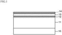
- FIG. 1 shows a schematic sectional view of the structure of a sample produced for verifying the above-described phenomenon.
- a GaN layer 11 with a thickness of 3 ⁇ m was formed on a sapphire substrate 10, and an InGaN layer (light emitting layer) 12 having a quantum well structure with a thickness of 3 nm was formed on the GaN layer 11. Further, a GaN layer (cap layer) 13 with a thickness of 10 nm was formed on the InGaN layer 12, and a SiO 2 film 14 with a thickness of 5 nm was formed on the GaN layer 13. Further, a surface of the SiO 2 film 14 was irradiated with a He-Cd laser (wavelength: 325 nm; intensity: 200 mW) for ten minutes.
- a He-Cd laser wavelength: 325 nm; intensity: 200 mW
- the GaN layer 11 and the GaN layer (cap layer) 13 were non-doped layers in the produced sample.
- the GaN layer 11 may be of an n-type
- the GaN layer (cap layer) 13 may be of a p-type.
- the In composition ratio of the InGaN layer (light emitting layer) 12 was adjusted such that blue light (470 nm), green light (510 nm), and yellow-green light (540 nm) are emitted.
- each of the GaN layer 11, the InGaN layer 12, and the GaN layer 13 was formed by metal organic chemical vapor deposition, and the SiO 2 film 14 was formed by sputtering.
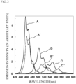
- FIG. 2 shows graphs of measurement results of the photoluminescence (PL) obtained in such a manner that the sample configured such that the SiO 2 film 14 is formed on the GaN layer (cap layer) 13 and a sample configured such that no SiO 2 film 14 is formed are irradiated with light from the He-Cd laser (wavelength: 325 nm; intensity: 200 mW).
- graphs indicated by solid lines A, B, C each show samples formed with SiO 2 films 14 and being capable of emitting blue light, green light, and yellow-green light.
- graphs indicated by dashed lines A', B', C' each show samples formed with no SiO 2 films 14 and being capable of emitting blue light, green light, and yellow-green light.
- FIG. 2 shows that as compared to the emission intensity of the sample formed with no SiO 2 film 14, the emission intensity of the sample formed with the SiO 2 film 14 is enhanced by about 1.5 times in the case of blue light emission, about 2.5 times in the case of green light emission, and about 13 times in the case of yellow-green light emission.
- FIG. 3 shows graphs of measurement results of the temperature dependence of the emission intensity for the yellow-green light emitting sample whose emission intensity was most enhanced.
- a graph indicated by black circles shows the sample formed with the SiO 2 film 14
- a graph indicated by black rectangles shows the sample formed with no SiO 2 film 14.
- the emission intensity increases as the temperature decreases, and shows a constant value at an extremely-low temperature. This is because motion of exciton by heat decreases as the temperature decreases, exciton is less likely to be captured by a nonradiative site due to, e.g., an impurity or dislocation/defect, and thermal inactivation leading to a decrease in the light emitting efficiency is reduced.
- the internal quantum efficiency of the emission when the emission intensity is constant at the extremely-low temperature is almost 100%, and by comparison with this value, the value of the internal quantum efficiency of the emission at each temperature can be estimated.
- the sample formed with no SiO 2 film 14 showed an internal quantum efficiency of 1.3% while the sample formed with the SiO 2 film 14 showed an internal quantum efficiency increased to 22%.
- FIG. 4 shows, for the yellow-green light emitting sample, graphs of measurement results of a change in the emission intensity for different laser irradiation times.
- graphs indicated by A 0 , A 1 , A 2 , A 3 , A 4 each show emission intensities when the laser irradiation time is zero minutes (no irradiation), one minute, three minutes, five minutes, and eight minutes.
- a graph indicated by B shows the sample formed with no SiO 2 film 14.
- FIG. 5 shows graphs obtained in such a manner the emission intensity is plotted for the laser irradiation time.
- FIG. 4 shows that the emission intensity increases as the laser irradiation time increases.
- FIG. 5 shows that the emission intensity is saturated after laser irradiation for a certain time. Note that even in the case of no laser irradiation (graph indicated by A 0 ), the emission intensity is improved by about five times as compared to the sample formed with no SiO 2 film 14.
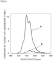
- FIG. 6 shows graphs of measurement results of the photoluminescence (PL) for a sample produced in such a manner that after the surface of the SiO 2 film 14 has been irradiated with the laser, the SiO 2 film 14 is removed from the GaN layer (cap layer) 13 using hydrofluoric acid.
- a graph indicated by A shows the sample from which the SiO 2 film 14 has been removed
- a graph indicated by B shows the sample formed with no SiO 2 film 14 in the first place.
- FIG. 6 shows that even the sample from which the SiO 2 film 14 has been removed maintains a high emission intensity which is substantially equal to that of the sample having the SiO 2 film 14 with the laser-irradiated surface.
- a sample was produced, which is configured such that a ZnO film with a thickness of 5 nm is formed as the oxide film 14 formed on the GaN layer (cap layer) 13 instead of the SiO 2 film.
- the ZnO film was formed by sputtering, and a configuration other than the ZnO film was the same as that of the sample shown in FIG. 1 .
- the In composition ratio of InGaN layer (light emitting layer) 12 was adjusted such that yellow-green light (540 nm) is emitted.
- a surface of the ZnO film was irradiated with a He-Cd layer (wavelength: 325 nm; intensity: 200 mW) for ten minutes.
- FIG. 7 shows graphs of measurement results of the photoluminescence (PL) obtained in such a manner that the sample configured such that the ZnO film is formed on the GaN layer (cap layer) 13 and a sample configured such that no ZnO film is formed are irradiated with light excited by the He-Cd laser (wavelength: 325 nm; intensity: 200 mW).
- a graph indicated by A 0 shows a sample for which no laser irradiation was performed after formation of the ZnO film
- a graph indicated by A 1 shows a sample for which laser irradiation was performed after formation of the ZnO film
- a graph indicated by B shows the sample formed with no ZnO film.
- FIG. 7 shows that as compared to the emission intensity of the sample formed with no ZnO film, the emission intensity of the sample for which laser irradiation was performed after formation of the ZnO film is enhanced by about seven times.
- FIG. 8 shows graphs of measurement results of a change in the emission intensity for different laser irradiation times.
- graphs indicated by A 0 , A 1 , A 2 , A 3 each show emission intensities when the laser irradiation time is zero minutes (no irradiation), one minute, three minutes, five minutes, and eight minutes.
- a graph indicated by B shows the sample formed with no ZnO film.
- FIG. 9 shows graphs obtained in such a manner the emission intensity is plotted for the laser irradiation time.
- FIG. 8 shows that the emission intensity increases as the laser irradiation time increases.
- FIG. 9 shows that the emission intensity is saturated after laser irradiation for a certain time. Note that even in the case of no laser irradiation (graph indicated by A 0 ), the emission intensity is improved by about three times as compared to the sample formed with no ZnO film.
- the above-described results show that the emission intensity is improved by formation of the particular oxide film (SiO 2 film or ZnO film) 14 on the GaN layer (cap layer) 13 and is significantly improved by laser irradiation of the surface of the oxide film (SiO 2 film or ZnO film) 14. Moreover, the results show that a high emission intensity is maintained even in a case where the oxide film (SiO 2 film or ZnO film) 14 is removed after laser irradiation.
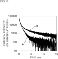
- FIG. 10 shows graphs of measurement results of a time-resolved emission profile for the sample configured such that the SiO 2 film 14 is formed on the GaN layer (cap layer) 13 and the same configured such that no SiO 2 film 14 is formed.
- a graph indicated by A shows the sample formed with the SiO 2 film 14
- a graph indicated by B shows the sample formed with no SiO 2 film 14.
- FIG. 10 shows that the sample formed with the SiO 2 film 14 has a shorter emission lifetime, and this means that an electron-hole pair recombination rate in the InGaN layer (light emitting layer) 12 increases.
- a cause for such an increase in the recombination rate is assumed to be improvement in the crystalline quality of the GaN layer (cap layer) 13 on the InGaN layer (light emitting layer) 12.
- the light emitting efficiency can be improved to a certain extent by formation of the SiO 2 film or the ZnO film as the oxide film 14 on the GaN layer (cap layer) 13, and is significantly improved by irradiation of the surface of the SiO 2 film or the ZnO film with the laser with a wavelength of 325 nm.
- the light emitting efficiency is not improved.
- a wavelength equivalent to the band gap of GaN is 365 nm, and therefore, when the surface of the SiO 2 film or the ZnO film is irradiated with the laser with a wavelength of 325 nm which is shorter than such a wavelength, light having penetrated the SiO 2 film or the ZnO film is absorbed by the GaN layer (cap layer) 13, the GaN layer (cap layer) 13 generates heat, and the temperature thereof increases. Accordingly, diffusion of Si or Zn from the SiO 2 film or the ZnO film into the crystals of the GaN layer (cap layer) 13 is promoted, and therefore, entrance into the Ga vacancies in the crystals of the GaN layer (cap layer) 13 is further promoted. As a result, the crystalline quality of the GaN layer (cap layer) 13 is further improved, the internal quantum efficiency of the InGaN layer (light emitting layer) 12 is improved, and the light emitting efficiency is improved.
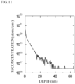
- FIG. 11 shows results of such measurement, and it was confirmed that Si is distributed with a concentration of 10 18 to 10 19 atoms/cm 3 in a region from the surface of the GaN layer to 20 nm, at which a quantum well related to light emission is present, in a depth direction.
- the bond between Al and O is not disconnected.
- the crystalline quality of the GaN layer (cap layer) 13 is not improved, and the effect of improving the light emitting efficiency is not obtained.
- the surface of the SiO 2 film or the ZnO film on the GaN layer (cap layer) 13 is preferably irradiated with laser which has a wavelength with an energy greater than the bond energy between Si or Zn and O (oxygen).
- the surface of the SiO 2 film or the ZnO film on the GaN layer (cap layer) 13 is preferably irradiated with laser which has a wavelength with an energy greater than the band gap energy of GaN.
- the light emitting efficiency is improved to a certain extent only by formation of the SiO 2 film or the ZnO film on the GaN layer (cap layer) by sputtering because it is assumed that in sputtering for forming the SiO 2 film or the ZnO film, a certain number of Si or Zn is diffused and enters the Ga vacancies in the vicinity of the surface of the GaN layer (cap layer) 13 and the crystalline quality of the GaN layer (cap layer) 13 is improved accordingly.
- FIGS. 12(A) to 12(C) show, for the sample configured such that the SiO 2 film with a thickness of 5 nm is formed on the GaN layer (cap layer) 13, graphs obtained in such a manner that emission intensities for different thicknesses of the GaN layer (cap layer) 13 are plotted for the laser irradiation time.
- FIGS. 12(A), 12(B), and 12(C) show samples configured such that the thicknesses of the GaN layer (cap layer) 13 are 5 nm, 25 nm, and 40 nm.
- FIGS. 12(A) to 12(C) show that the time until the emission intensity is saturated increases as the thickness of the GaN layer (cap layer) increases. This may be because a time until Si diffused into the GaN layer (cap layer) 13 by laser irradiation reaches the InGaN layer (light emitting layer) 12 increases and a time until the crystalline quality of the GaN layer (cap layer) 13 is improved increases accordingly.
- FIG. 13 shows graphs of measurement results of a ratio (emission intensity ratio) between the emission intensity of the sample shown in FIG. 1 and configured such that the SiO 2 film 14 is formed on the GaN layer (cap layer) 13 and the emission intensity of the sample formed with no SiO 2 film for different thicknesses of the GaN layer (cap layer) 13.
- FIG. 13 shows that the emission intensity ratio is improved as the thickness of the GaN layer (cap layer) 13 increases.
- the thickness of the GaN layer (cap layer) 13 is preferably 5 nm or more. If the thickness of the GaN layer (cap layer) 13 is less than 5 nm, it is not preferred because the InGaN layer (light emitting layer) 12 receives damage due to sputtering for forming the SiO 2 film 14 and the effect of improving the light emitting efficiency cannot be obtained.
- the thickness of the GaN layer (cap layer) 13 is preferably 150 nm or less. If the thickness of the GaN layer (cap layer) 13 exceeds 150 nm, it is not preferred because a distance between the InGaN layer (light emitting layer) 12 and the SiO 2 film 14 extremely increases, Si is not diffused to the vicinity of the InGaN layer (light emitting layer) 12, and the effect of improving the light emitting efficiency cannot be obtained. Further, the thickness of the GaN layer (cap layer) 13 is more preferably 100 nm or less.
- a distance by which the laser with a wavelength of 325 nm can enter the GaN layer (cap layer) 13 is about 100 nm, and therefore, if the thickness of the GaN layer (cap layer) 13 exceeds 100 nm, it is not preferred because a sufficient temperature increase by heat generation of the GaN layer (cap layer) 13 cannot be achieved and the effect of improving the light emitting efficiency cannot be obtained.
- the thickness of the oxide film (SiO 2 film or ZnO film) 14 on the GaN layer (cap layer) 13 is preferably 1 nm or more because it is difficult to form a thin film if the thickness of less than 1 nm.
- a method for producing the light emitting device in the present invention includes a step of forming the light emitting layer 12 having the quantum well structure on the substrate 10, a step of forming the cap layer 13 made of GaN on the light emitting layer 12, and a step of forming the oxide film 14 on the cap layer 13.
- the oxide film 14 is made of an oxide having an element which can be diffused and enter the Ga vacancies in the cap layer 13 made of GaN.
- the oxide film 14 is preferably the SiO 2 film or the ZnO film, and is preferably formed by sputtering.
- the method preferably further includes a step of irradiating the surface of the oxide film 14 on the cap layer 13 with light which has a wavelength with a greater energy than a bond energy between the element (Si in the case of the SiO 2 film, Zn in the case of the ZnO film) forming the oxide film 14 and oxygen.
- the method may further include a step of removing the oxide film 14 from the cap layer 13.
- At least one or both of the element forming the oxide film 14 and oxygen are present.
- the light emitting device made of the GaN semiconductor can have the improved light emitting efficiency.
- the light emitting device can be provided, which has a high light emitting efficiency in the wavelength range of green light (510 nm) or yellow-green light (540 nm).
- FIG. 14 shows a schematic sectional view of the configuration of the light emitting device (light emitting diode) produced by the method for producing the light emitting device in the present invention.
- the light emitting device 1 includes the n-type GaN layer 11 formed on the substrate 10, the light emitting layer 12 formed on the n-type GaN layer 11 and having the quantum well structure, the cap layer 13 formed on the light emitting layer 12 and made of p-type GaN, and the ZnO film 14 formed on the cap layer 13.
- the ZnO film 14 is preferably a film formed by sputtering. Moreover, the surface of the ZnO film 14 is preferably irradiated with light which has a wavelength with a greater energy than a bond energy between zinc (Zn) and oxygen (O).
- the ZnO film 14 has conductivity, and therefore, a transparent electrode film 15 is formed on the ZnO film 14 and electrodes 20, 21 are each formed on the transparent electrode film 15 and the n-type GaN layer 11 so that current can be injected into the light emitting layer 12 and light can be taken out from the light emitting layer 12.
- the SiO 2 film is an insulating film.
- the SiO 2 film is removed from the cap layer 13, and thereafter, the transparent electrode film 15 is formed on the cap layer 13 and the electrodes 20, 21 are each formed on the transparent electrode film 15 and the n-type GaN layer 11.
- current can be injected into the light emitting layer 12, and light can be taken out from the light emitting layer 12.
- the effect of improving the light emitting efficiency is maintained even after the SiO 2 film has been removed from the cap layer 13, and therefore, the light emitting device having a high light emitting efficiency can be obtained.
- FIG. 16 shows a sectional view of a variation of the light emitting device in the present invention.
- the light emitting device 1 shown in FIG. 16 is different from the light emitting device 1 shown in FIG. 14 in that a plasmon layer 30 that plasmon-resonates with light emitted from the light emitting layer 12 is further formed on the ZnO film 14.
- the plasmon layer 30 is formed of a metal thin film or metal fine particles made of a material such as Ag, Al, Au, or Cu.
- Non-Patent Document 1 Non-Patent Document 1
- metal atoms are diffused from the metal thin film or the metal fine particles forming the plasmon layer 30 into the p-type GaN layer 13, the structure of the plasmon layer 30 is broken over time, and the plasmon effect is degraded.
- the light emitting device 1 in the present variation is configured such that the plasmon layer 30 is formed on the p-type GaN layer (cap layer) 13 through the ZnO film 14, and therefore, diffusion of the metal atoms from, e.g., the metal thin film forming the plasmon layer 30 into the p-type GaN layer 13 can be prevented. Accordingly, the structure of the plasmon layer 30 can be stabilized, and the plasmon effect can be maintained.
- the light emitting device 1 of the present variation not only the light emitting efficiency can be improved by formation of the ZnO film 14 on the p-type GaN layer 13, but also the light emitting efficiency can be further improved by formation of the plasmon layer 30 on the ZnO film 14. Thus, the light emitting device 1 having a higher light emitting efficiency can be provided.
- the thickness of the ZnO film 14 is preferably 10 nm or less.
- the oxide film 14 such as the SiO 2 film or the ZnO film is formed on the p-type GaN layer (cap layer) 13, but a nitride film such as a Si 3 N 4 film may be formed.
- a surface of the Si 3 N 4 film is irradiated with laser which has a wavelength with a greater energy than a bond energy between Si and N (nitrogen), and in this manner, the bond between Si and N is disconnected and Si is diffused and enters the Ga vacancies in the p-type GaN layer (cap layer) 13. Accordingly, the crystalline quality of the p-type GaN layer (cap layer) 13 is improved.
- the InGaN layer having the single quantum well structure has been described as an example of the light emitting layer 12, but the present invention is not limited thereto and an InGaN layer having a multiple quantum well structure may be used.
- the light emitting layer 12 is not limited to the InGaN layer, and, e.g., an AlGaN layer may be used.
- the light emitting diode has been described as an example of the light emitting device 1, but the present invention is not limited thereto and is also applicable to, e.g., a semiconductor laser.
Landscapes
- Led Devices (AREA)
Abstract
Description
- The present invention relates to a method for producing a light emitting device made of GaN-based semiconductor and a light emitting device.
- As a light emitting device, such as a light emitting diode, made of GaN-based semiconductor, there has been known a light emitting device including a light emitting layer having a quantum well structure and made of InGaN.
- InGaN is a mixed crystal of GaN and InN, and the band gap energy thereof can be changed by adjustment of the composition ratio thereof. In this manner, an emission wavelength can be controlled. However, under the current circumstances, a high light emitting efficiency is obtained in a blue spectral range, but the light emitting efficiency is extremely low in other ranges.
- As an approach for improving the light emitting efficiency, there has been proposed a method using surface plasmon resonance (Non-Patent Document 1). In this method, a method a metal thin film is formed in the vicinity of an InGaN light emitting layer with a GaN layer (cap layer) interposed therebetween, and upon light emission by recombination, an electron-hole pair in the InGaN light emitting layer resonates with surface plasmon at an interface between the metal thin film and the GaN layer, and a light emitting rate increases. As a result, the light emitting efficiency is improved.
- NON-PATENT DOCUMENT 1: Applied Physics Letters, vol. 87, 7110,
- In the method using the surface plasmon resonance, light from the light emitting layer is absorbed by the metal thin film, and therefore, there is a problem that an optical loss is great and there is no metal material suitable for a green spectral range.
- The present invention has been made in view of the above-described point, and an object thereof is to provide a method for producing a light emitting device made of GaN-based semiconductor and having an improved light emitting efficiency and provide a light emitting device.
- The method for producing the light emitting device according to the present invention is a method for producing a light emitting device made of GaN-based semiconductor, the method including a step of forming a light emitting layer having a quantum well structure on a substrate, a step of forming a cap layer made of GaN on the light emitting layer, and a step of forming an oxide film on the cap layer. The oxide film is made of oxide having an element which can be diffused and enter a Ga vacancy in the cap layer made of GaN.
- The light emitting device according to the present invention is a light emitting device made of GaN-based semiconductor, the light emitting device including a light emitting layer having a quantum well structure, a cap layer formed on the light emitting layer and made of GaN, and a ZnO film formed on the cap layer.
- According to the present invention, the method for producing the light emitting device made of the GaN-based semiconductor and having the improved light emitting efficiency and the light emitting device can be provided.
-
- [
FIG. 1] FIG. 1 shows a schematic sectional view of the structure of a sample produced for describing the present invention. - [
FIG. 2] FIG. 2 shows graphs of measurement results of photoluminescence (PL) obtained in such a manner that a sample configured such that a SiO2 film is formed on a GaN layer (cap layer) is irradiated with excitation light. - [
FIG. 3] FIG. 3 shows graphs of measurement results of the temperature dependence of an emission intensity for a yellow-green light emitting sample. - [
FIG. 4] FIG. 4 shows graphs of measurement results of a change in the emission intensity for different laser irradiation times for the yellow-green light emitting sample. - [
FIG. 5] FIG. 5 shows graphs obtained in such a manner that the emission intensity is plotted for the laser irradiation time. - [
FIG. 6] FIG. 6 shows graphs of measurement results of the photoluminescence (PL) for a sample from which the SiO2 film is removed after laser irradiation of a surface of the SiO2 film. - [
FIG. 7] FIG. 7 shows graphs of measurement results of the photoluminescence (PL) for a sample configured such that a ZnO film is formed on the GaN layer (cap layer). - [
FIG. 8] FIG. 8 shows graphs of measurement results of a change in the emission intensity for different laser irradiation times. - [
FIG. 9] FIG. 9 shows graphs obtained in such a manner that the emission intensity is plotted for the laser irradiation time. - [
FIG. 10] FIG. 10 shows graphs of measurement results of a time-resolved emission profile for the sample configured such that the SiO2 film is formed on the GaN layer (cap layer). - [
FIG. 11] FIG. 11 shows graphs of measurement results of a Si concentration in the GaN layer (cap layer). - [
FIG. 12] FIGS. 12(A) to 12(C) show graphs obtained in such a manner that emission intensities for different thicknesses of the GaN layer (cap layer) are plotted for the laser irradiation time. - [
FIG. 13] FIG. 13 shows graphs of measurement results of an emission intensity ratio between the sample configured such that the SiO2 film is formed on the GaN layer (cap layer) and a sample formed with no SiO2 film for different thicknesses of the GaN layer (cap layer). - [
FIG. 14] FIG. 14 shows a schematic sectional view of the configuration of a light emitting device of the present invention. - [
FIG. 15] FIG. 15 shows a schematic sectional view of another configuration of the light emitting device of the present invention. - [
FIG. 16] FIG. 16 shows a sectional view of a variation of the light emitting device of the present invention. - The inventors et al. of the present application have found such a remarkable phenomenon that a light emitting efficiency is significantly improved by formation of an oxide film made of a particular material on a surface of a GaN layer formed on a surface of an InGaN light emitting layer instead of formation of a metal thin film.
-
FIG. 1 shows a schematic sectional view of the structure of a sample produced for verifying the above-described phenomenon. - As shown in
FIG. 1 , aGaN layer 11 with a thickness of 3 µm was formed on asapphire substrate 10, and an InGaN layer (light emitting layer) 12 having a quantum well structure with a thickness of 3 nm was formed on theGaN layer 11. Further, a GaN layer (cap layer) 13 with a thickness of 10 nm was formed on theInGaN layer 12, and a SiO2 film 14 with a thickness of 5 nm was formed on theGaN layer 13. Further, a surface of the SiO2 film 14 was irradiated with a He-Cd laser (wavelength: 325 nm; intensity: 200 mW) for ten minutes. Note that in order to check light emission from the sample according to a later-described photoluminescence (PL), theGaN layer 11 and the GaN layer (cap layer) 13 were non-doped layers in the produced sample. Note that in a case where a light emitting device such as an LED is formed, the GaNlayer 11 may be of an n-type, and the GaN layer (cap layer) 13 may be of a p-type. - Here, the In composition ratio of the InGaN layer (light emitting layer) 12 was adjusted such that blue light (470 nm), green light (510 nm), and yellow-green light (540 nm) are emitted. Moreover, each of the GaN
layer 11, the InGaNlayer 12, and the GaNlayer 13 was formed by metal organic chemical vapor deposition, and the SiO2 film 14 was formed by sputtering. -
FIG. 2 shows graphs of measurement results of the photoluminescence (PL) obtained in such a manner that the sample configured such that the SiO2 film 14 is formed on the GaN layer (cap layer) 13 and a sample configured such that no SiO2 film 14 is formed are irradiated with light from the He-Cd laser (wavelength: 325 nm; intensity: 200 mW). Here, graphs indicated by solid lines A, B, C each show samples formed with SiO2 films 14 and being capable of emitting blue light, green light, and yellow-green light. Moreover, graphs indicated by dashed lines A', B', C' each show samples formed with no SiO2 films 14 and being capable of emitting blue light, green light, and yellow-green light. -
FIG. 2 shows that as compared to the emission intensity of the sample formed with no SiO2 film 14, the emission intensity of the sample formed with the SiO2 film 14 is enhanced by about 1.5 times in the case of blue light emission, about 2.5 times in the case of green light emission, and about 13 times in the case of yellow-green light emission. -
FIG. 3 shows graphs of measurement results of the temperature dependence of the emission intensity for the yellow-green light emitting sample whose emission intensity was most enhanced. Here, a graph indicated by black circles shows the sample formed with the SiO2 film 14, and a graph indicated by black rectangles shows the sample formed with no SiO2 film 14. - As shown in
FIG. 3 , the emission intensity increases as the temperature decreases, and shows a constant value at an extremely-low temperature. This is because motion of exciton by heat decreases as the temperature decreases, exciton is less likely to be captured by a nonradiative site due to, e.g., an impurity or dislocation/defect, and thermal inactivation leading to a decrease in the light emitting efficiency is reduced. Thus, it is assumed that the internal quantum efficiency of the emission when the emission intensity is constant at the extremely-low temperature is almost 100%, and by comparison with this value, the value of the internal quantum efficiency of the emission at each temperature can be estimated. Thus, the sample formed with no SiO2 film 14 showed an internal quantum efficiency of 1.3% while the sample formed with the SiO2 film 14 showed an internal quantum efficiency increased to 22%. -
FIG. 4 shows, for the yellow-green light emitting sample, graphs of measurement results of a change in the emission intensity for different laser irradiation times. Here, graphs indicated by A0, A1, A2, A3, A4 each show emission intensities when the laser irradiation time is zero minutes (no irradiation), one minute, three minutes, five minutes, and eight minutes. Note that a graph indicated by B shows the sample formed with no SiO2 film 14. Moreover,FIG. 5 shows graphs obtained in such a manner the emission intensity is plotted for the laser irradiation time. -
FIG. 4 shows that the emission intensity increases as the laser irradiation time increases. Moreover,FIG. 5 shows that the emission intensity is saturated after laser irradiation for a certain time. Note that even in the case of no laser irradiation (graph indicated by A0), the emission intensity is improved by about five times as compared to the sample formed with no SiO2 film 14. -
FIG. 6 shows graphs of measurement results of the photoluminescence (PL) for a sample produced in such a manner that after the surface of the SiO2 film 14 has been irradiated with the laser, the SiO2 film 14 is removed from the GaN layer (cap layer) 13 using hydrofluoric acid. Here, a graph indicated by A shows the sample from which the SiO2 film 14 has been removed, and a graph indicated by B shows the sample formed with no SiO2 film 14 in the first place. -
FIG. 6 shows that even the sample from which the SiO2 film 14 has been removed maintains a high emission intensity which is substantially equal to that of the sample having the SiO2 film 14 with the laser-irradiated surface. - A sample was produced, which is configured such that a ZnO film with a thickness of 5 nm is formed as the
oxide film 14 formed on the GaN layer (cap layer) 13 instead of the SiO2 film. The ZnO film was formed by sputtering, and a configuration other than the ZnO film was the same as that of the sample shown inFIG. 1 . The In composition ratio of InGaN layer (light emitting layer) 12 was adjusted such that yellow-green light (540 nm) is emitted. Moreover, a surface of the ZnO film was irradiated with a He-Cd layer (wavelength: 325 nm; intensity: 200 mW) for ten minutes. -
FIG. 7 shows graphs of measurement results of the photoluminescence (PL) obtained in such a manner that the sample configured such that the ZnO film is formed on the GaN layer (cap layer) 13 and a sample configured such that no ZnO film is formed are irradiated with light excited by the He-Cd laser (wavelength: 325 nm; intensity: 200 mW). Here, a graph indicated by A0 shows a sample for which no laser irradiation was performed after formation of the ZnO film, a graph indicated by A1 shows a sample for which laser irradiation was performed after formation of the ZnO film, and a graph indicated by B shows the sample formed with no ZnO film. -
FIG. 7 shows that as compared to the emission intensity of the sample formed with no ZnO film, the emission intensity of the sample for which laser irradiation was performed after formation of the ZnO film is enhanced by about seven times. -
FIG. 8 shows graphs of measurement results of a change in the emission intensity for different laser irradiation times. Here, graphs indicated by A0, A1, A2, A3 each show emission intensities when the laser irradiation time is zero minutes (no irradiation), one minute, three minutes, five minutes, and eight minutes. Note that a graph indicated by B shows the sample formed with no ZnO film. Moreover,FIG. 9 shows graphs obtained in such a manner the emission intensity is plotted for the laser irradiation time. -
FIG. 8 shows that the emission intensity increases as the laser irradiation time increases. Moreover,FIG. 9 shows that the emission intensity is saturated after laser irradiation for a certain time. Note that even in the case of no laser irradiation (graph indicated by A0), the emission intensity is improved by about three times as compared to the sample formed with no ZnO film. - Even the sample from which the ZnO film was removed after laser irradiation maintained a high emission intensity which is substantially equal to that of the sample having the ZnO film with the laser-irradiated surface.
- The above-described results show that the emission intensity is improved by formation of the particular oxide film (SiO2 film or ZnO film) 14 on the GaN layer (cap layer) 13 and is significantly improved by laser irradiation of the surface of the oxide film (SiO2 film or ZnO film) 14. Moreover, the results show that a high emission intensity is maintained even in a case where the oxide film (SiO2 film or ZnO film) 14 is removed after laser irradiation.
- A reason why the light emitting efficiency is improved to a certain extent by formation of the SiO2 film or the ZnO film on the GaN layer (cap layer) 13 and is significantly improved by laser irradiation of the surface of the SiO2 film or the ZnO film is not known exactly, but it is assumed that such a phenomenon occurs due to the following mechanism.
-
FIG. 10 shows graphs of measurement results of a time-resolved emission profile for the sample configured such that the SiO2 film 14 is formed on the GaN layer (cap layer) 13 and the same configured such that no SiO2 film 14 is formed. Here, a graph indicated by A shows the sample formed with the SiO2 film 14, and a graph indicated by B shows the sample formed with no SiO2 film 14. -
FIG. 10 shows that the sample formed with the SiO2 film 14 has a shorter emission lifetime, and this means that an electron-hole pair recombination rate in the InGaN layer (light emitting layer) 12 increases. A cause for such an increase in the recombination rate is assumed to be improvement in the crystalline quality of the GaN layer (cap layer) 13 on the InGaN layer (light emitting layer) 12. - As described above, the light emitting efficiency can be improved to a certain extent by formation of the SiO2 film or the ZnO film as the
oxide film 14 on the GaN layer (cap layer) 13, and is significantly improved by irradiation of the surface of the SiO2 film or the ZnO film with the laser with a wavelength of 325 nm. On the other hand, in a case where an Al2O3 film is formed as another oxide film on the GaN layer (cap layer) 13, the light emitting efficiency is not improved. - Normally, there are Ga vacancies in the
GaN layer 13, and these Ga vacancies influence the light emitting efficiency of the InGaN layer (light emitting layer) 12. As shown in Table 1, the covalent radii of Si, Zn, and Al are similar to or less than the covalent radius of Ga, and therefore, Si, Zn, and Al in the SiO2 film, the ZnO film, and Al2O3 film can be diffused into the Ga vacancies in theGaN layer 13.[Table 1] Element Covalent Radius (A) Ga 1.22 Si 1.11 Zn 1.22 Al 1.18 - An effect of significantly improving the light emitting efficiency is obtained by irradiation with the laser with a wavelength of 325 nm, and this wavelength is equivalent to an energy of 3.8 eV. As shown in Table 2, this energy is higher than a bond energy (3.1 eV) between Si and O (oxygen) and a bond energy (2.2 eV) between Zn and O (oxygen), and is lower than a bond energy (5.3 eV) between Al and O (oxygen).
[Table 2] Bond Type Bond Energy [eV] Si-O 3.1 Zn-O 2.2 Al-O 5.3 - In view of the above-described points, it is assumed that the bond between Si or Zn and O is disconnected by irradiation of the surface of the SiO2 film or the ZnO film with the laser with a wavelength of 325 nm, Si or Zn is diffused and enters the Ga vacancies in the crystals of the GaN layer (cap layer) 13, and the crystalline quality of the GaN layer (cap layer) 13 is improved accordingly. As a result, the internal quantum efficiency of the InGaN layer (light emitting layer) 12 is improved, and the light emitting efficiency is improved.
- In addition, a wavelength equivalent to the band gap of GaN is 365 nm, and therefore, when the surface of the SiO2 film or the ZnO film is irradiated with the laser with a wavelength of 325 nm which is shorter than such a wavelength, light having penetrated the SiO2 film or the ZnO film is absorbed by the GaN layer (cap layer) 13, the GaN layer (cap layer) 13 generates heat, and the temperature thereof increases. Accordingly, diffusion of Si or Zn from the SiO2 film or the ZnO film into the crystals of the GaN layer (cap layer) 13 is promoted, and therefore, entrance into the Ga vacancies in the crystals of the GaN layer (cap layer) 13 is further promoted. As a result, the crystalline quality of the GaN layer (cap layer) 13 is further improved, the internal quantum efficiency of the InGaN layer (light emitting layer) 12 is improved, and the light emitting efficiency is improved.
- In order to verify the above-described mechanism, measurement of elements in the GaN layer (cap layer) by secondary ion mass spectrometry (SIMS) was performed for the sample having the SiO2 film with the surface irradiated with the laser after formation of the SiO2 film (thickness: 5 nm) on the GaN layer (thickness: 10 nm) 13. Note that measurement was performed after removal of the SiO2 film from the
GaN layer 13. -
FIG. 11 shows results of such measurement, and it was confirmed that Si is distributed with a concentration of 1018 to 1019 atoms/cm3 in a region from the surface of the GaN layer to 20 nm, at which a quantum well related to light emission is present, in a depth direction. - On the other hand, even when the surface of the Al2O3 film is irradiated with the laser with a wavelength of 325 nm, the bond between Al and O is not disconnected. Thus, the crystalline quality of the GaN layer (cap layer) 13 is not improved, and the effect of improving the light emitting efficiency is not obtained.
- Note that in order to obtain the effect of improving the light emitting efficiency by laser irradiation, the surface of the SiO2 film or the ZnO film on the GaN layer (cap layer) 13 is preferably irradiated with laser which has a wavelength with an energy greater than the bond energy between Si or Zn and O (oxygen). Moreover, the surface of the SiO2 film or the ZnO film on the GaN layer (cap layer) 13 is preferably irradiated with laser which has a wavelength with an energy greater than the band gap energy of GaN.
- Note that not only the Ga vacancies but also N vacancies are present in the vicinity of the surface of the GaN layer (cap layer) 13, and therefore, it is assumed that O disconnected from Si or Zn is diffused into the N vacancies and the crystalline quality of the GaN layer (cap layer) 13 is improved accordingly.
- The light emitting efficiency is improved to a certain extent only by formation of the SiO2 film or the ZnO film on the GaN layer (cap layer) by sputtering because it is assumed that in sputtering for forming the SiO2 film or the ZnO film, a certain number of Si or Zn is diffused and enters the Ga vacancies in the vicinity of the surface of the GaN layer (cap layer) 13 and the crystalline quality of the GaN layer (cap layer) 13 is improved accordingly.
-
FIGS. 12(A) to 12(C) show, for the sample configured such that the SiO2 film with a thickness of 5 nm is formed on the GaN layer (cap layer) 13, graphs obtained in such a manner that emission intensities for different thicknesses of the GaN layer (cap layer) 13 are plotted for the laser irradiation time.FIGS. 12(A), 12(B), and 12(C) show samples configured such that the thicknesses of the GaN layer (cap layer) 13 are 5 nm, 25 nm, and 40 nm. -
FIGS. 12(A) to 12(C) show that the time until the emission intensity is saturated increases as the thickness of the GaN layer (cap layer) increases. This may be because a time until Si diffused into the GaN layer (cap layer) 13 by laser irradiation reaches the InGaN layer (light emitting layer) 12 increases and a time until the crystalline quality of the GaN layer (cap layer) 13 is improved increases accordingly. -
FIG. 13 shows graphs of measurement results of a ratio (emission intensity ratio) between the emission intensity of the sample shown inFIG. 1 and configured such that the SiO2 film 14 is formed on the GaN layer (cap layer) 13 and the emission intensity of the sample formed with no SiO2 film for different thicknesses of the GaN layer (cap layer) 13. -
FIG. 13 shows that the emission intensity ratio is improved as the thickness of the GaN layer (cap layer) 13 increases. Note that the thickness of the GaN layer (cap layer) 13 is preferably 5 nm or more. If the thickness of the GaN layer (cap layer) 13 is less than 5 nm, it is not preferred because the InGaN layer (light emitting layer) 12 receives damage due to sputtering for forming the SiO2 film 14 and the effect of improving the light emitting efficiency cannot be obtained. - Moreover, the thickness of the GaN layer (cap layer) 13 is preferably 150 nm or less. If the thickness of the GaN layer (cap layer) 13 exceeds 150 nm, it is not preferred because a distance between the InGaN layer (light emitting layer) 12 and the SiO2 film 14 extremely increases, Si is not diffused to the vicinity of the InGaN layer (light emitting layer) 12, and the effect of improving the light emitting efficiency cannot be obtained. Further, the thickness of the GaN layer (cap layer) 13 is more preferably 100 nm or less. A distance by which the laser with a wavelength of 325 nm can enter the GaN layer (cap layer) 13 is about 100 nm, and therefore, if the thickness of the GaN layer (cap layer) 13 exceeds 100 nm, it is not preferred because a sufficient temperature increase by heat generation of the GaN layer (cap layer) 13 cannot be achieved and the effect of improving the light emitting efficiency cannot be obtained.
- In the present invention, the thickness of the oxide film (SiO2 film or ZnO film) 14 on the GaN layer (cap layer) 13 is preferably 1 nm or more because it is difficult to form a thin film if the thickness of less than 1 nm.
- A method for producing the light emitting device in the present invention includes a step of forming the
light emitting layer 12 having the quantum well structure on thesubstrate 10, a step of forming thecap layer 13 made of GaN on thelight emitting layer 12, and a step of forming theoxide film 14 on thecap layer 13. Theoxide film 14 is made of an oxide having an element which can be diffused and enter the Ga vacancies in thecap layer 13 made of GaN. - The
oxide film 14 is preferably the SiO2 film or the ZnO film, and is preferably formed by sputtering. - The method preferably further includes a step of irradiating the surface of the
oxide film 14 on thecap layer 13 with light which has a wavelength with a greater energy than a bond energy between the element (Si in the case of the SiO2 film, Zn in the case of the ZnO film) forming theoxide film 14 and oxygen. - The method may further include a step of removing the
oxide film 14 from thecap layer 13. - In the
cap layer 13, at least one or both of the element forming theoxide film 14 and oxygen are present. - According to the method for producing the light emitting device in the present invention, the light emitting device made of the GaN semiconductor can have the improved light emitting efficiency. Particularly, the light emitting device can be provided, which has a high light emitting efficiency in the wavelength range of green light (510 nm) or yellow-green light (540 nm).
-
FIG. 14 shows a schematic sectional view of the configuration of the light emitting device (light emitting diode) produced by the method for producing the light emitting device in the present invention. - As shown in
FIG. 14 , thelight emitting device 1 includes the n-type GaN layer 11 formed on thesubstrate 10, thelight emitting layer 12 formed on the n-type GaN layer 11 and having the quantum well structure, thecap layer 13 formed on thelight emitting layer 12 and made of p-type GaN, and theZnO film 14 formed on thecap layer 13. - Here, the
ZnO film 14 is preferably a film formed by sputtering. Moreover, the surface of theZnO film 14 is preferably irradiated with light which has a wavelength with a greater energy than a bond energy between zinc (Zn) and oxygen (O). - The
ZnO film 14 has conductivity, and therefore, atransparent electrode film 15 is formed on theZnO film 14 andelectrodes transparent electrode film 15 and the n-type GaN layer 11 so that current can be injected into thelight emitting layer 12 and light can be taken out from thelight emitting layer 12. - In a case where the SiO2 film is formed on the
cap layer 13, the SiO2 film is an insulating film. Thus, as shown inFIG. 15 , the SiO2 film is removed from thecap layer 13, and thereafter, thetransparent electrode film 15 is formed on thecap layer 13 and theelectrodes transparent electrode film 15 and the n-type GaN layer 11. In this manner, current can be injected into thelight emitting layer 12, and light can be taken out from thelight emitting layer 12. Note that the effect of improving the light emitting efficiency is maintained even after the SiO2 film has been removed from thecap layer 13, and therefore, the light emitting device having a high light emitting efficiency can be obtained. -
FIG. 16 shows a sectional view of a variation of the light emitting device in the present invention. - The
light emitting device 1 shown inFIG. 16 is different from thelight emitting device 1 shown inFIG. 14 in that aplasmon layer 30 that plasmon-resonates with light emitted from thelight emitting layer 12 is further formed on theZnO film 14. Here, theplasmon layer 30 is formed of a metal thin film or metal fine particles made of a material such as Ag, Al, Au, or Cu. - It has been known that the
plasmon layer 30 is formed on the surface of the p-type GaN layer 13 on the InGaNlight emitting layer 12 so that the light emitting efficiency can be improved by a plasmon effect (Non-Patent Document 1), but there is a problem that metal atoms are diffused from the metal thin film or the metal fine particles forming theplasmon layer 30 into the p-type GaN layer 13, the structure of theplasmon layer 30 is broken over time, and the plasmon effect is degraded. - As shown in
FIG. 16 , thelight emitting device 1 in the present variation is configured such that theplasmon layer 30 is formed on the p-type GaN layer (cap layer) 13 through theZnO film 14, and therefore, diffusion of the metal atoms from, e.g., the metal thin film forming theplasmon layer 30 into the p-type GaN layer 13 can be prevented. Accordingly, the structure of theplasmon layer 30 can be stabilized, and the plasmon effect can be maintained. - In the
light emitting device 1 of the present variation, not only the light emitting efficiency can be improved by formation of theZnO film 14 on the p-type GaN layer 13, but also the light emitting efficiency can be further improved by formation of theplasmon layer 30 on theZnO film 14. Thus, thelight emitting device 1 having a higher light emitting efficiency can be provided. - Note that in the present variation, if the thickness of the
ZnO film 14 is too great, the electric field of theplasmon layer 30 does not reach the InGaNlight emitting layer 12 and the plasmon effect is not provided. For this reason, the thickness of theZnO film 14 is preferably 10 nm or less. - The present invention has been described above with reference to the preferred embodiments, but is not limited to such description. Needless to say, various modifications can be made. For example, in the above-described embodiments, the
oxide film 14 such as the SiO2 film or the ZnO film is formed on the p-type GaN layer (cap layer) 13, but a nitride film such as a Si3N4 film may be formed. In this case, for example, a surface of the Si3N4 film is irradiated with laser which has a wavelength with a greater energy than a bond energy between Si and N (nitrogen), and in this manner, the bond between Si and N is disconnected and Si is diffused and enters the Ga vacancies in the p-type GaN layer (cap layer) 13. Accordingly, the crystalline quality of the p-type GaN layer (cap layer) 13 is improved. - In the above-described embodiments, the InGaN layer having the single quantum well structure has been described as an example of the
light emitting layer 12, but the present invention is not limited thereto and an InGaN layer having a multiple quantum well structure may be used. Moreover, thelight emitting layer 12 is not limited to the InGaN layer, and, e.g., an AlGaN layer may be used. - In the above-described embodiments, the light emitting diode has been described as an example of the
light emitting device 1, but the present invention is not limited thereto and is also applicable to, e.g., a semiconductor laser. -
- 1
- Light Emitting Device
- 10
- Substrate
- 11
- (n-type) GaN Layer
- 12
- InGaN Layer (Light Emitting Layer)
- 13
- (p-type) GaN Layer (Cap Layer)
- 14
- Oxide Film (SiO2 Film, ZnO Film)
- 15
- Transparent Electrode Film
- 20, 21
- Electrode
- 30
- Plasmon Layer
Claims (18)
- A method for producing a light emitting device made of GaN-based semiconductor, comprising:a step of forming a light emitting layer having a quantum well structure on a substrate;a step of forming a cap layer made of GaN on the light emitting layer; anda step of forming an oxide film on the cap layer,wherein the oxide film is made of oxide having an element which is able to be diffused and enter a Ga vacancy in the cap layer made of GaN.
- The method for producing the light emitting device according to claim 1, wherein
the oxide film is formed by sputtering. - The method for producing the light emitting device according to claim 1, further comprising:
a step of irradiating a surface of the oxide film on the cap layer with light which has a wavelength with a greater energy than a bond energy between the element and oxygen forming the oxide film. - The method for producing the light emitting device according to claim 1, further comprising:
a step of irradiating a surface of the oxide film on the cap layer with laser which has a wavelength with a greater energy than a band gap energy of GaN. - The method for producing the light emitting device according to claim 1, further comprising:
a step of removing the oxide film from the cap layer. - The method for producing the light emitting device according to claim 1, further comprising:
a step of forming, on a surface of the oxide film, a plasmon layer that plasmon-resonates with light emitted from the light emitting layer. - The method for producing the light emitting device according to claim 1, wherein
after the step of forming the oxide film on the cap layer, at least one or both of the element and oxygen forming the oxide film are present in the cap layer. - The method for producing the light emitting device according to claim 1, wherein
the oxide film is a SiO2 film or a ZnO film. - The method for producing the light emitting device according to claim 1, wherein
a thickness of the oxide film is 1 nm or more. - The method for producing the light emitting device according to claim 1, wherein
a thickness of the cap layer is within a range of 5 nm to 150 nm. - The method for producing the light emitting device according to claim 6, wherein
the plasmon layer is formed of a metal thin film or metal fine particles. - A light emitting device made of GaN-based semiconductor, comprising:a light emitting layer having a quantum well structure;a cap layer formed on the light emitting layer and made of GaN; anda ZnO film formed on the cap layer.
- The light emitting device according to claim 12, wherein
the ZnO film is a film formed by sputtering. - The light emitting device according to claim 12, wherein
a thickness of the cap layer is within a range of 5 nm to 150 nm. - The light emitting device according to claim 12, wherein
a surface of the ZnO film is irradiated with light which has a wavelength with a greater energy than a bond energy between zinc (Zn) and oxygen (O). - The light emitting device according to claim 12, wherein
at least one or both of zinc (Zn) and oxygen (O) are present in the cap layer. - The light emitting device according to claim 12, further comprising:
on the ZnO film, a plasmon layer that plasmon-resonates with light emitted from the light emitting layer. - The light emitting device according to claim 17, wherein
the plasmon layer is formed of a metal thin film or metal fine particles.
Applications Claiming Priority (2)
| Application Number | Priority Date | Filing Date | Title |
|---|---|---|---|
| JP2022014115 | 2022-02-01 | ||
| PCT/JP2023/003083 WO2023149433A1 (en) | 2022-02-01 | 2023-01-31 | Method for producing light emitting element, and light emitting element |
Publications (2)
| Publication Number | Publication Date |
|---|---|
| EP4475198A1 true EP4475198A1 (en) | 2024-12-11 |
| EP4475198A4 EP4475198A4 (en) | 2025-11-12 |
Family
ID=87552478
Family Applications (1)
| Application Number | Title | Priority Date | Filing Date |
|---|---|---|---|
| EP23749749.0A Pending EP4475198A4 (en) | 2022-02-01 | 2023-01-31 | METHOD FOR PRODUCEING A LIGHT EMISSIONING ELEMENT AND LIGHT EMISSIONING ELEMENT |
Country Status (5)
| Country | Link |
|---|---|
| US (1) | US20260231567A1 (en) |
| EP (1) | EP4475198A4 (en) |
| JP (1) | JP7841716B2 (en) |
| CN (1) | CN118613925A (en) |
| WO (1) | WO2023149433A1 (en) |
Family Cites Families (17)
| Publication number | Priority date | Publication date | Assignee | Title |
|---|---|---|---|---|
| JP4306041B2 (en) * | 1999-08-25 | 2009-07-29 | 昭和電工株式会社 | Group III nitride semiconductor light emitting device |
| JP2006506827A (en) * | 2002-11-16 | 2006-02-23 | エルジー イノテック カンパニー リミテッド | Optical device and manufacturing method thereof |
| JP4451811B2 (en) * | 2005-05-09 | 2010-04-14 | ローム株式会社 | Manufacturing method of nitride semiconductor device |
| JP5103979B2 (en) * | 2007-03-27 | 2012-12-19 | 豊田合成株式会社 | Electrode forming method for group III nitride compound semiconductor and method for producing p-type group III nitride compound semiconductor |
| TWI363440B (en) * | 2007-11-01 | 2012-05-01 | Univ Nat Taiwan | Light-emitting device, light-emitting diode and method for forming a light-emitting device |
| JP2009239217A (en) * | 2008-03-28 | 2009-10-15 | Nikon Corp | Light-emitting diode element |
| TWI382568B (en) * | 2009-06-16 | 2013-01-11 | Univ Nat Taiwan | Light-emitting element, light-emitting diode |
| JP2011035275A (en) * | 2009-08-04 | 2011-02-17 | Panasonic Corp | Nitride semiconductor light-emitting element |
| JP5170030B2 (en) * | 2009-08-11 | 2013-03-27 | 日立電線株式会社 | Nitride semiconductor free-standing substrate, nitride semiconductor free-standing substrate manufacturing method, and nitride semiconductor device |
| CN102792471A (en) * | 2010-04-01 | 2012-11-21 | 松下电器产业株式会社 | Light-emitting diode element and light-emitting diode device |
| JP2012015156A (en) * | 2010-06-29 | 2012-01-19 | Kyocera Corp | Light emitting element |
| US8314439B2 (en) * | 2011-02-11 | 2012-11-20 | Sharp Kabushiki Kaisha | Light emitting diode with nanostructures and method of making the same |
| CN102593305B (en) * | 2012-03-21 | 2014-10-15 | 电子科技大学 | Metal periodic subwavelength structure on surface of light-emitting diode (LED) and preparation method for metal periodic subwavelength structure |
| JP2013201326A (en) * | 2012-03-26 | 2013-10-03 | Hitachi Cable Ltd | Gallium nitride substrate and epitaxial wafer |
| KR20140061827A (en) * | 2012-11-14 | 2014-05-22 | 삼성전자주식회사 | Semiconductor light emitting device and manufacturing method of semiconductor light emitting device |
| KR101600783B1 (en) * | 2014-05-23 | 2016-03-08 | 광주과학기술원 | Method of fabricating light emitting diode with high efficiency |
| KR102000271B1 (en) * | 2017-04-19 | 2019-10-01 | 전북대학교산학협력단 | PREPARING METHOD OF GaN TYPE LIGHT EMITTING DIODE AND GaN TYPE LIGHT EMITTING DIODE PREPARED THEREFROM |
-
2023
- 2023-01-31 WO PCT/JP2023/003083 patent/WO2023149433A1/en not_active Ceased
- 2023-01-31 JP JP2023578566A patent/JP7841716B2/en active Active
- 2023-01-31 CN CN202380018842.7A patent/CN118613925A/en active Pending
- 2023-01-31 US US18/834,918 patent/US20260231567A1/en active Pending
- 2023-01-31 EP EP23749749.0A patent/EP4475198A4/en active Pending
Also Published As
| Publication number | Publication date |
|---|---|
| CN118613925A (en) | 2024-09-06 |
| JP7841716B2 (en) | 2026-04-07 |
| EP4475198A4 (en) | 2025-11-12 |
| WO2023149433A1 (en) | 2023-08-10 |
| US20260231567A1 (en) | 2026-08-06 |
| KR20240132039A (en) | 2024-09-02 |
| JPWO2023149433A1 (en) | 2023-08-10 |
Similar Documents
| Publication | Publication Date | Title |
|---|---|---|
| US7812366B1 (en) | Ultraviolet light emitting AlGaN composition, and ultraviolet light emitting device containing same | |
| KR100406201B1 (en) | Light-emitting gallium nitride-based compound semiconductor device | |
| CN1132253C (en) | GaN-based semiconductor light-emitting element and manufacturing method thereof | |
| Salvador et al. | Near ultraviolet luminescence of Be doped GaN grown by reactive molecular beam epitaxy using ammonia | |
| KR102009535B1 (en) | Method for producing an optoelectronic semiconductor chip and optoelectronic semiconductor chip | |
| US10685835B2 (en) | III-nitride tunnel junction with modified P-N interface | |
| CN1474485A (en) | Laser diode | |
| JP2009152644A (en) | Method for activating compound semiconductor thin film to p-type | |
| US6429102B1 (en) | Method of manufacturing low resistivity p-type compound semiconductor material | |
| US7041519B2 (en) | Method for producing p-type group III nitride compound semiconductor | |
| CN115377267A (en) | Ultraviolet semiconductor light emitting element | |
| KR20080003870A (en) | Manufacturing method of nitride semiconductor device | |
| EP3236505A1 (en) | Light emitting element | |
| US20230023759A1 (en) | Optoelectronic component and method for producing the same | |
| CN1119358A (en) | Blue-green laser diode | |
| CN102369605B (en) | Light emitting diode element and method for producing the same | |
| JP2010098194A (en) | Phosphor, light-emitting element, light-emitting device, and method for producing phosphor | |
| KR100827993B1 (en) | Gallium nitride-based semiconductor device | |
| JP7565028B2 (en) | Method for manufacturing light-emitting device and method for removing hydrogen from light-emitting device | |
| JP7841716B2 (en) | Method for manufacturing a light-emitting element and a light-emitting element | |
| US20100038656A1 (en) | Nitride LEDs based on thick templates | |
| US7847314B2 (en) | Gallium nitride-based compound semiconductor light-emitting device | |
| US20200098649A1 (en) | Method for producing semiconductor device | |
| CN108054247A (en) | A kind of improvement GaN epitaxy piece property simultaneously enhances the method for GaN base LED luminescent properties | |
| EP1130659A1 (en) | Method of manufacturing low resistivity p-type compound semiconductor material |
Legal Events
| Date | Code | Title | Description |
|---|---|---|---|
| STAA | Information on the status of an ep patent application or granted ep patent |
Free format text: STATUS: THE INTERNATIONAL PUBLICATION HAS BEEN MADE |
|
| PUAI | Public reference made under article 153(3) epc to a published international application that has entered the european phase |
Free format text: ORIGINAL CODE: 0009012 |
|
| STAA | Information on the status of an ep patent application or granted ep patent |
Free format text: STATUS: REQUEST FOR EXAMINATION WAS MADE |
|
| 17P | Request for examination filed |
Effective date: 20240813 |
|
| AK | Designated contracting states |
Kind code of ref document: A1 Designated state(s): AL AT BE BG CH CY CZ DE DK EE ES FI FR GB GR HR HU IE IS IT LI LT LU LV MC ME MK MT NL NO PL PT RO RS SE SI SK SM TR |
|
| DAV | Request for validation of the european patent (deleted) | ||
| DAX | Request for extension of the european patent (deleted) | ||
| REG | Reference to a national code |
Ref country code: DE Ref legal event code: R079 Free format text: PREVIOUS MAIN CLASS: H01L0033320000 Ipc: H10H0020810000 |
|
| A4 | Supplementary search report drawn up and despatched |
Effective date: 20251015 |
|
| RIC1 | Information provided on ipc code assigned before grant |
Ipc: H10H 20/81 20250101AFI20251009BHEP Ipc: H10H 20/84 20250101ALI20251009BHEP Ipc: H10H 20/01 20250101ALI20251009BHEP |