EP4475183A1 - Semiconductor structure and method for forming same - Google Patents
Semiconductor structure and method for forming same Download PDFInfo
- Publication number
- EP4475183A1 EP4475183A1 EP22944507.7A EP22944507A EP4475183A1 EP 4475183 A1 EP4475183 A1 EP 4475183A1 EP 22944507 A EP22944507 A EP 22944507A EP 4475183 A1 EP4475183 A1 EP 4475183A1
- Authority
- EP
- European Patent Office
- Prior art keywords
- layer
- forming
- region
- word line
- trench
- Prior art date
- Legal status (The legal status is an assumption and is not a legal conclusion. Google has not performed a legal analysis and makes no representation as to the accuracy of the status listed.)
- Granted
Links
Images





Classifications
-
- H—ELECTRICITY
- H10—SEMICONDUCTOR DEVICES; ELECTRIC SOLID-STATE DEVICES NOT OTHERWISE PROVIDED FOR
- H10B—ELECTRONIC MEMORY DEVICES
- H10B12/00—Dynamic random access memory [DRAM] devices
- H10B12/01—Manufacture or treatment
- H10B12/02—Manufacture or treatment for one transistor one-capacitor [1T-1C] memory cells
- H10B12/03—Making the capacitor or connections thereto
-
- H—ELECTRICITY
- H10—SEMICONDUCTOR DEVICES; ELECTRIC SOLID-STATE DEVICES NOT OTHERWISE PROVIDED FOR
- H10B—ELECTRONIC MEMORY DEVICES
- H10B12/00—Dynamic random access memory [DRAM] devices
- H10B12/01—Manufacture or treatment
- H10B12/02—Manufacture or treatment for one transistor one-capacitor [1T-1C] memory cells
- H10B12/05—Making the transistor
-
- H—ELECTRICITY
- H10—SEMICONDUCTOR DEVICES; ELECTRIC SOLID-STATE DEVICES NOT OTHERWISE PROVIDED FOR
- H10B—ELECTRONIC MEMORY DEVICES
- H10B12/00—Dynamic random access memory [DRAM] devices
- H10B12/30—DRAM devices comprising one-transistor - one-capacitor [1T-1C] memory cells
- H10B12/48—Data lines or contacts therefor
- H10B12/482—Bit lines
-
- H—ELECTRICITY
- H10—SEMICONDUCTOR DEVICES; ELECTRIC SOLID-STATE DEVICES NOT OTHERWISE PROVIDED FOR
- H10W—GENERIC PACKAGES, INTERCONNECTIONS, CONNECTORS OR OTHER CONSTRUCTIONAL DETAILS OF DEVICES COVERED BY CLASS H10
- H10W20/00—Interconnections in chips, wafers or substrates
- H10W20/40—Interconnections external to wafers or substrates, e.g. back-end-of-line [BEOL] metallisations or vias connecting to gate electrodes
- H10W20/45—Interconnections external to wafers or substrates, e.g. back-end-of-line [BEOL] metallisations or vias connecting to gate electrodes characterised by their insulating parts
- H10W20/48—Insulating materials thereof
Definitions
- DRAM Dynamic random access memory
- a gate of the transistor is electrically connected to a word line
- a source is electrically connected to a bit line
- a drain is electrically connected to the capacitor.
- Word line voltage applied on the word line can control on and off of the transistor, so that the bit line can be used to read data stored in the capacitor or write data into the capacitor.
- DRAM and other semiconductor structures mostly are two-dimensional structures, resulting in low storage density and integration of the semiconductor structure, which can hardly meet the requirements of semiconductor storage capacity in different fields.
- a semiconductor structure and a method for forming the semiconductor structure are provided in some embodiments of this invention to mitigate the problem of relatively low integration of a semiconductor structure, so as to improve the performance of the semiconductor structure and expand the application field of the semiconductor structure.
- this invention provides a method for forming a semiconductor structure, including the following steps: forming a stacking layer on a top surface of a substrate, where the stacking layer includes a plurality of semiconductor layers arranged at intervals in a first direction, and the stacking layer includes a transistor region, a capacitor region distributed on two opposite sides of the transistor region in a second direction, and a bit line region, where the semiconductor layers include semiconductor columns arranged at intervals in a third direction, where the first direction is perpendicular to the top surface of the substrate, both of the second direction and the third direction are parallel to the top surface of the substrate, and the second direction intersects the third direction; forming, in the capacitor region, a capacitor extending in the second direction; forming a word line in the transistor region, where the word line extends in the third direction and continuously covers the semiconductor columns arranged at intervals in the third direction; and forming a bit line in the bit line region, where the bit line extends in the first direction and is electrically connected to the semiconductor columns
- the step of forming a stacking layer on a top surface of a substrate includes: alternately depositing the semiconductor layer and a first sacrificial layer on the top surface of the substrate in the first direction to form the stacking layer; and etching the stacking layer to form a first trench exposing the substrate, where the first trench separates the semiconductor layers into the semiconductor columns arranged at intervals in the third direction.
- each semiconductor column includes a conductive column located in the capacitor region
- the step of forming, in the capacitor region, a capacitor extending in the second direction includes: removing the first sacrificial layer in the capacitor region to form a first gap between two adjacent semiconductor layers in the capacitor region; forming, in the first gap, a conductive layer covering the conductive column, a dielectric layer covering the conductive layer, an upper electrode layer covering the dielectric layer, and a common electrode layer covering the upper electrode layer; and forming a capacitor including the conductive column, the conductive layer, the dielectric layer, the upper electrode layer, and the common electrode layer.
- the step of forming a capacitor including the conductive column, the conductive layer, the dielectric layer, the upper electrode layer, and the common electrode layer includes: forming a conductive layer that continuously covers inner walls of the first gaps arranged at intervals in the first direction; forming a dielectric layer covering a surface of the conductive layer; forming an upper electrode layer covering a surface of the dielectric layer; forming a common electrode layer covering a surface of the upper electrode layer; removing the conductive layer, the dielectric layer, the upper electrode layer, and the common electrode layer that cover a sidewall of the first sacrificial layer in the transistor region; and forming a first opening between two adjacent semiconductor layers in the capacitor region, where the conductive column, and the conductive layer, the dielectric layer, the upper electrode layer, and the common electrode layer that remain in the first gap form the capacitor.
- a bottom of the second trench exposes the top surface of the substrate; or the second trench extends to the inside of the substrate.
- the stacking layer includes two transistor regions distributed on two opposite sides of the bit line region in the second direction, and one capacitor region is located on a side of the transistor region that is away from the bit line region, and where the step of removing the first sacrificial layer in the transistor region along the second trench includes: simultaneously removing the first sacrificial layers in the two transistor regions along the second trench.
- the step of forming, in the second gap, the word line that extends in the third direction and continuously covers the channel regions arranged at intervals in the third direction includes: forming an initial word line layer that covers an inner wall of the second gap and an inner wall of the second trench, where the initial word line layer continuously covers at least the active columns arranged at intervals in the third direction; forming an isolation layer that covers a surface of the initial word line layer and fills the second gap and the second trench; and removing the initial word line layer and the isolation layer that are located in the second trench and above the source region and the drain region, to form a second opening between two adjacent drain regions and a third opening between two adjacent source regions, where the initial word line layer remaining above the channel region is configured as the word line, and the isolation layer remaining between two adjacent word lines is configured as a word line isolation layer.
- the stacking layer includes the semiconductor layer and a first sacrificial layer that are alternately stacked in the first direction, where the semiconductor columns include an active column located in the transistor region, and the active column includes a channel region, and where a thickness of the first sacrificial layer in the first direction is four times greater than a width of a gap between two adjacent channel regions in the semiconductor layer in the third direction.
- the step of forming an initial word line layer that covers an inner wall of the second gap and an inner wall of the second trench includes: forming, by using a lateral atomic layer deposition process, the initial word line layer that covers the inner wall of the second gap and the inner wall of the second trench.
- the method before the bit line is formed in the bit line region, the method further includes the following steps: removing the capacitor isolation layer; forming a dielectric layer that fills the first opening, the second opening, the third opening, and the second trench; and removing the dielectric layer in the second trench.
- the step of forming, in the second gap, the word line that extends in the third direction and continuously covers the channel regions arranged at intervals in the third direction includes: depositing a gate material on an inner wall of the second gap and an inner wall of the second trench along the second trench to form an initial gate layer that covers the active column, where two adjacent initial gate layers in the third direction are independent of each other; depositing an initial word line material along the second trench to form an initial word line layer that covers a surface of the initial gate layer, where the initial word line layer continuously covers at least the active columns arranged at intervals in the third direction; forming an isolation layer that covers a surface of the initial word line layer and fills the second gap and the second trench; and removing the initial gate layer, the initial word line layer, and the isolation layer that are located in the second trench and above the source region and the drain region, to form a second opening between two adjacent drain regions and a third opening between two adjacent source regions, where the initial gate layer remaining above the channel region is configured as a gate layer, the initial word line
- a material of the semiconductor layer is a silicon material doped with ions.
- this invention further provides a semiconductor structure formed by using the method for forming a semiconductor structure according to any of the foregoing embodiments.
- the stacking layer is formed on the top surface of the substrate.
- the stacking layer includes a plurality of semiconductor layers arranged at intervals in a direction perpendicular to the top surface of the substrate, and each semiconductor layer includes a plurality of semiconductor columns arranged at intervals in a direction parallel to the top surface of the substrate, so that the plurality of semiconductor columns in the stacking layer are stacked in a three-dimensional array.
- a horizontal capacitor, a horizontal word line, and a vertical bit line are formed to convert a conventional two-dimensional semiconductor structure into a three-dimensional semiconductor structure.
- FIG. 1 is a flowchart of a method for forming a semiconductor structure according to an embodiment of this invention.
- FIG. 2 to FIG. 23 are schematic diagrams of main structures in a process of forming a semiconductor structure according to various embodiments of this invention.
- the semiconductor structure provided in these embodiments may be but is not limited to a DRAM.
- the method for forming a semiconductor structure includes the following steps.
- Step S11 Form a stacking layer 21 on a top surface of a substrate 20, where the stacking layer 21 includes a plurality of semiconductor layers 212 arranged at intervals in a first direction D1, and the stacking layer 21 includes a transistor region, a capacitor region distributed on two opposite sides of the transistor region in a second direction D2, and a bit line region.
- the semiconductor layers 212 include semiconductor columns 26 arranged at intervals in a third direction D3.
- the first direction D1 is perpendicular to the top surface of the substrate 20, both of the second direction D2 and the third direction D3 are parallel to the top surface of the substrate 20, and the second direction D2 intersects the third direction D3.
- image (a) of FIG. 5 is a schematic top view of a semiconductor structure
- image (b) of FIG. 5 is a schematic cross-sectional diagram of image (a) of FIG. 5 along AA direction.
- the substrate 20 may be but is not limited to a silicon substrate. Some embodiments are described by using an example in which the substrate 20 is a silicon substrate. In some other embodiments, the substrate 20 may be a semiconductor substrate such as gallium nitride, gallium arsenide, gallium carbide, silicon carbide, or SOI. The substrate 20 is configured to support a semiconductor component above the substrate 20. The top surface of the substrate 20 refers to a surface of the substrate 20 used to form the stacking layer 21.
- the step of forming a stacking layer 21 on a top surface of a substrate 20 includes: alternately depositing the semiconductor layer 212 and a first sacrificial layer 211 on the top surface of the substrate 20 in the first direction D1 to form the stacking layer 21 as shown in FIG. 2 , where image (a) of FIG. 2 is a schematic top view of a semiconductor structure, and image (b) of FIG. 2 is a schematic cross-sectional diagram of image (a) of FIG. 2 along AA direction; and etching the stacking layer 21 to form a first trench 25 exposing the substrate 20, where the first trench 25 separates the semiconductor layers 212 into the semiconductor columns 26 arranged at intervals in the third direction D3, as shown in FIG. 5 .
- the doped ions may be but are not limited to phosphorus ions.
- ions do not need to be doped when a channel region, a source region, and a drain region in the transistor are subsequently formed, thereby simplifying the forming process of the semiconductor structure.
- the material of the first pad layer 22 may be but is not limited to an oxide material (such as silicon dioxide), and the material of the second pad layer 23 may be but is not limited to a nitride material (such as silicon nitride).
- oxide material such as silicon dioxide
- nitride material such as silicon nitride
- a patterned first photoresist layer 24 is formed on a surface of the second pad layer 23, and the first photoresist layer 24 has a first etching window 241 exposing the second pad layer 23.
- image (a) of FIG. 4 is a schematic top view of a semiconductor structure
- image (b) of FIG. 4 is a schematic cross-sectional diagram of image (a) of FIG. 4 along AA direction.
- the second pad layer 23, the first pad layer 22, and the stacking layer 21 are etched downward along the first etching window 241 to form a plurality of first trenches 25 exposing the substrate 20, and the plurality of first trenches 25 are arranged at intervals in the third direction D3, so that each semiconductor layer 212 is separated into a plurality of semiconductor columns 26 arranged at intervals in the third direction D3, and each first sacrificial layer 211 is separated into a plurality of sacrificial columns 27 arranged at intervals in the third direction D3, as shown in FIG. 5 .
- the first pad layer 22 and the second pad layer 23 are configured to improve a morphology of the first trench.
- the first pad layer 22 and the second pad layer 23 are further configured to prevent a processing of patterning the first photoresist layer 24 from damaging the semiconductor layer 212 in a topmost layer of the stacking layer 21.
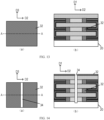
- each semiconductor column 26 includes a conductive column 261 located in the capacitor region, and the step of forming, in the capacitor region, a capacitor extending in the second direction D2 includes: removing the first sacrificial layer 211 in the capacitor region to form a first gap 29 between two adjacent semiconductor layers 212 in the capacitor region as shown in FIG. 8 , where image (a) of FIG. 8 is a schematic top view of a semiconductor structure, and image (b) of FIG. 8 is a schematic cross-sectional diagram of image (a) of FIG.
- the step of forming a capacitor including the conductive column 261, the conductive layer 301, the dielectric layer 302, the upper electrode layer 303, and the common electrode layer 304 includes: forming a conductive layer 301 that continuously covers inner walls of the first gaps 29 arranged at intervals in the first direction D1; forming a dielectric layer 302 covering a surface of the conductive layer 301; forming an upper electrode layer 303 covering a surface of the dielectric layer 302 as shown in FIG. 9 , where image (a) of FIG. 9 is a schematic top view of a semiconductor structure, and image (b) of FIG. 9 is a schematic cross-sectional diagram of image (a) of FIG.
- image (a) of FIG. 10 is a schematic top view of a semiconductor structure
- image (b) of FIG. 10 is a schematic cross-sectional diagram of image (a) of FIG.
- a third sacrificial layer 28 is formed on the surface of the second pad layer 23 as shown in FIG. 6 .
- Image (a) of FIG. 6 is a schematic top view of a semiconductor structure
- image (b) of FIG. 6 is a schematic cross-sectional diagram of image (a) of FIG. 6 along AA direction.
- the material of the third sacrificial layer 28 may be but is not limited to an oxide material (such as silicon dioxide).
- a patterned second photoresist layer is formed on a surface of the third sacrificial layer 28, and the second photoresist layer has a second etching window exposing the third sacrificial layer 28.
- the third sacrificial layer 28 is etched downward along the second etching window to expose the second pad layer 23 above the transistor region as shown in FIG. 7 .
- Image (a) of FIG. 7 is a schematic top view of a semiconductor structure
- image (b) of FIG. 7 is a schematic cross-sectional diagram of image (a) of FIG. 7 along AA direction.
- the remaining third sacrificial layer 28 covers stacking layer 21 in the transistor region and the bit line region.
- the first sacrificial layer 211 in the capacitor region may be removed by using a lateral etching process to form the first gap 29 between two adjacent semiconductor layers 212 in the capacitor region, as shown in FIG. 8 . Forming the first gap 29 by using the lateral etching process can simplify the manufacturing process of the semiconductor structure and avoid damage to the stacking layer 21 in the transistor region and the bit line region.
- a conductive material such as metal tungsten or TiN is continuously deposited by using a lateral atomic layer deposition process on inner walls of a plurality of first gaps 29 arranged at intervals in the first direction D1, to form the conductive layer 301 that continuously covers surfaces of a plurality of conductive columns 261 arranged at intervals in the first direction D1.
- a material with a relatively high dielectric constant (HK) is deposited on the surface of the conductive layer 301 to form the dielectric layer 302.
- a conductive material such as metal tungsten or TiN is deposited on the surface of the dielectric layer 302 to form the upper electrode layer 303, as shown in FIG. 9 .
- a conductive material such as polycrystalline silicon is deposited in the first gap 29 to form the common electrode layer 304 that covers the upper electrode layer 303 and fills the first gap 29, as shown in FIG. 10 .
- a structure shown in FIG. 11 is obtained after the first pad layer 22, the second pad layer 23, the third sacrificial layer 28, the conductive layer 301, the dielectric layer 302, the upper electrode layer 303, and the common electrode layer 304 are removed from the top surface of the stacking layer 21, where image (a) of FIG. 11 is a schematic top view of a semiconductor structure, and image (b) of FIG. 11 is a schematic cross-sectional diagram of image (a) of FIG. 11 along AA direction.
- a patterned third photoresist layer is formed above the stacking layer 21, and the third photoresist layer includes a third etching window exposing a portion of the conductive layer 301, the dielectric layer 302, the upper electrode layer 303, and the common electrode layer 304.
- the conductive layer 301, the dielectric layer 302, the upper electrode layer 303, and the common electrode layer 304 are etched downward along the third etching window, to remove the conductive layer 301, the dielectric layer 302, the upper electrode layer 303, and the common electrode layer 304 that cover the sidewall of the first sacrificial layer 211 in the transistor region, and form the first opening 31 between two adjacent semiconductor layers 212 in the capacitor region, where the conductive column 261, and the conductive layer 301, the dielectric layer 302, the upper electrode layer 303, and the common electrode layer 304 that remain in the first gap 29 form the capacitor, as shown in FIG. 12 .
- the conductive column 261 and the conductive layer 301 jointly serve as a lower electrode layer of the capacitor.
- image (a) of FIG. 13 is a schematic top view of a semiconductor structure
- image (b) of FIG. 13 is a schematic cross-sectional diagram of image (a) of FIG. 13 along AA direction.
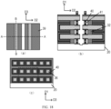
- Step S13 Form a word line 40 in the transistor region, where the word line 40 extends in the third direction D3 and continuously covers the semiconductor columns 26 arranged at intervals in the third direction D3 as shown in FIG. 18 , where image (a) of FIG. 18 is a schematic top view of a semiconductor structure, image (b) of FIG. 18 is a schematic cross-sectional diagram of image (a) of FIG. 18 along AA direction, and image (c) of FIG. 18 is a schematic cross-sectional diagram of image (a) of FIG. 18 along BB direction.
- each semiconductor column 26 includes an active column 36 located in the transistor region (refer to FIG. 18 ), the active column 36 includes a channel region, and a source region and a drain region distributed on two opposite sides of the channel region in the second direction D2, the drain region is adjacent to the capacitor region, and the source region is adjacent to the bit line region.
- the step of forming a word line 40 in the transistor region includes: removing the first sacrificial layer 211 in the transistor region and the stacking layer 21 in the bit line region; forming a second gap 35 exposing at least the channel region in the transistor region and a second trench 34 exposing the substrate 20 in the bit line region as shown in FIG. 15 , where image (a) of FIG.
- image (b) of FIG. 15 is a schematic cross-sectional diagram of image (a) of FIG. 15 along AA direction
- image (c) of FIG. 15 is a schematic cross-sectional diagram of image (a) of FIG. 15 along BB direction; and forming, in the second gap 35, the word line 40 that extends in the third direction D3 and continuously covers the channel regions arranged at intervals in the third direction D3, as shown in FIG. 18 .
- the step of forming a second gap 35 exposing at least the channel region in the transistor region and a second trench 34 exposing the substrate in the bit line region includes: forming a capacitor isolation layer 32 filling the first opening 31; removing the stacking layer 21 in the bit line region to form the second trench 34 exposing the substrate 20 in the bit line region as shown in FIG. 14 , where image (a) of FIG. 14 is a schematic top view of a semiconductor structure, and image (b) of FIG. 14 is a schematic cross-sectional diagram of image (a) of FIG.
- a bottom of the second trench 34 exposes the top surface of the substrate 20.
- the substrate 20 is configured as an etching stop layer in an etching process, to accurately control an etching endpoint and avoid damage to the substrate 20.
- the second trench 34 extends to the inside of the substrate 20 to enlarge the area of contact between a bit line subsequently formed in the second trench 34 and the substrate 20.
- the stacking layer 21 includes two transistor regions distributed on two opposite sides of the bit line region in the second direction D2, and one capacitor region is located on a side of the transistor region that is away from the bit line region.
- the step of removing the first sacrificial layer 211 in the transistor region along the second trench 34 includes: simultaneously removing the first sacrificial layers 211 in the two transistor regions along the second trench 34.
- one bit line region is disposed in the stacking layer 21, and one transistor region is disposed on each of the two opposite sides of the bit line region in the second direction D2, and one capacitor region is disposed on the side of the transistor region that is away from the bit line region, so that two subsequently formed transistors can share one bit line, thereby further reducing the size of the semiconductor structure and improving integration of the semiconductor structure.
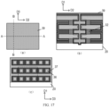
- the step of forming, in the second gap 35, the word line 40 that extends in the third direction D3 and continuously covers the channel regions arranged at intervals in the third direction D3 includes: forming an initial word line layer 37 that covers an inner wall of the second gap 35 and an inner wall of the second trench 34, where the initial word line layer 37 continuously covers at least the active columns 36 arranged at intervals in the third direction D3 as shown in FIG. 16 , where image (a) of FIG. 16 is a schematic top view of a semiconductor structure, image (b) of FIG. 16 is a schematic cross-sectional diagram of image (a) of FIG. 16 along AA direction, image (c) of FIG. 16 is a schematic cross-sectional diagram of image (a) of FIG.
- image (d) of FIG. 16 is an enlarged schematic diagram of image (c) of FIG. 16 in a dashed-line frame; forming an isolation layer 39 that covers a surface of the initial word line layer 37 and fills the second gap 35 and the second trench 34 as shown in FIG. 17 , where image (a) of FIG. 17 is a schematic top view of a semiconductor structure, image (b) of FIG. 17 is a schematic cross-sectional diagram of image (a) of FIG. 17 along AA direction, and image (c) of FIG. 17 is a schematic cross-sectional diagram of image (a) of FIG.
- the step of forming an initial word line layer 37 that covers an inner wall of the second gap 35 and an inner wall of the second trench 34 includes: forming, by using a lateral atomic layer deposition process, the initial word line layer 37 that covers the inner wall of the second gap 35 and the inner wall of the second trench 34.
- a gate dielectric layer 38 covering a surface of the active column 36 may be formed through in-situ steam oxidation or by using a lateral deposition process, as shown in FIG. 16 . Then, a conductive material such as metal tungsten or TiN is deposited on a surface of the gate dielectric layer 38 by using a lateral atomic layer deposition process, to form the initial word line layer 37 that covers the inner wall of the second gap 35 and the inner wall of the second trench 34.
- the lateral deposition process can ensure that the initial word line layer 37 fully covers the inner wall of the second gap 35, thereby further improving electrical performance of the semiconductor structure.
- the stacking layer 21 includes the semiconductor layer 212 and a first sacrificial layer 211 that are alternately stacked in the first direction D1, where the semiconductor columns 26 include an active column 36 located in the transistor region, and the active column 36 includes a channel region.
- the thickness A of the first sacrificial layer 211 in the first direction D1 is four times greater than the width B of a gap between two adjacent channel regions in the semiconductor layer 212 in the third direction D3, that is, A>4B.
- the thickness A of the first sacrificial layer 211 in the first direction D1 is set to be four times greater than the width B of the gap between two adjacent channel regions in the semiconductor layer 212 in the third direction D3, so that when word line materials used to form the initial word line layer 37 are deposited, the word line materials are first connected in a line in the third direction D3, to ensure that the ultimately formed word line 40 extends in the third direction D3 and can fully and continuously covers the channel regions arranged at intervals in the semiconductor layer 212 in the third direction D3.
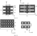
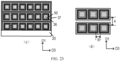
- the step of forming, in the second gap 35, the word line 40 that extends in the third direction D3 and continuously covers the channel regions arranged at intervals in the third direction D3 includes: depositing a gate material on an inner wall of the second gap 35 and an inner wall of the second trench 34 along the second trench 34 to form an initial gate layer 50 that covers the active column 36, where two adjacent initial gate layers 50 in the third direction D3 are independent of each other as shown in FIG. 22 , where image (c) of FIG. 22 is a schematic diagram of a cross-sectional structure, and image (d) of FIG. 22 is an enlarged schematic diagram of image (c) of FIG.
- a gate dielectric layer covering a surface of the active column 36 may be formed through in-situ steam oxidation or by using a lateral deposition process. Then, a conductive material such as TiN is deposited on a surface of the gate dielectric layer by using a lateral atomic layer deposition process, to form the initial gate layer 50 located above the gate dielectric layer.
- a plurality of initial gate layers 50 are respectively located above a plurality of channel regions, and any two adjacent initial gate layers 50 are independent of each other.
- a conductive material such as metal tungsten is deposited on the surface of the initial gate layer 50 by using the lateral atomic layer deposition process, to form the initial word line layer 37 that continuously covers at least the active columns 36 arranged at intervals in the third direction D3.
- the initial gate layer 50 is first formed, so that in one aspect, it's further ensured that the subsequently formed initial word line layer 37 can fully and continuously cover the channel regions arranged at intervals in the third direction D3, and in another aspect, adhesion between the initial word line layer 37 and the initial gate layer 50 can be further enhanced.
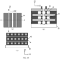
- Step S14 Form a bit line 44 in the bit line region, where the bit line 44 extends in the first direction D1 and is electrically connected to the semiconductor columns 26 arranged at intervals in the first direction D1 as shown in FIG. 21 , where image (a) of FIG. 21 is a schematic top view of a semiconductor structure, image (b) of FIG. 21 is a schematic cross-sectional diagram of image (a) of FIG. 21 along AA direction, and image (c) of FIG. 21 is a schematic cross-sectional diagram of image (a) of FIG. 21 along BB direction.
- the method before the bit line is formed in the bit line region, the method further includes the following steps: removing the capacitor isolation layer 32 as shown in FIG. 19 , where image (a) of FIG. 19 is a schematic top view of a semiconductor structure, image (b) of FIG. 19 is a schematic cross-sectional diagram of image (a) of FIG. 19 along AA direction, and image (c) of FIG. 19 is a schematic cross-sectional diagram of image (a) of FIG. 19 along BB direction; forming a dielectric layer 43 that fills the first opening 31, the second opening, the third opening, and the second trench 34 as shown in FIG. 20 , where image (a) of FIG. 20 is a schematic top view of a semiconductor structure, image (b) of FIG.
- FIG. 20 is a schematic cross-sectional diagram of image (a) of FIG. 20 along AA direction, and image (c) of FIG. 20 is a schematic cross-sectional diagram of image (a) of FIG. 20 along BB direction; and removing the dielectric layer 43 in the second trench 34.
- a conductive material such as metal tungsten may be deposited in the second trench 34 to form the bit line 44 that extends in the first direction D1 and is electrically connected to the source region in the semiconductor columns 26 arranged at intervals in the first direction D1.
- One bit line 44 is electrically connected to two source regions located on two opposite sides of the bit line 44 in the second direction D2.
- An embodiment further provides a semiconductor structure, and the semiconductor structure may be formed by using the method for forming a semiconductor structure described according to FIG. 1 to FIG. 23 .
- a schematic diagram of the semiconductor structure provided in this embodiment may refer to FIG. 21 .
- the stacking layer is formed on the top surface of the substrate, where the stacking layer includes a plurality of semiconductor layers arranged at intervals in a direction perpendicular to the top surface of the substrate, and each semiconductor layer includes a plurality of semiconductor columns arranged at intervals in a direction parallel to the top surface of the substrate, so that the plurality of semiconductor columns in the stacking layer are stacked in a three-dimensional array.
- a horizontal capacitor, a horizontal word line, and a vertical bit line are formed to convert a conventional two-dimensional semiconductor structure into a three-dimensional semiconductor structure.
Landscapes
- Engineering & Computer Science (AREA)
- Manufacturing & Machinery (AREA)
- Semiconductor Memories (AREA)
Abstract
Description
- This application claims priority to
Chinese Patent Application No. 202210614481.X, filed on May 30, 2022 - This invention relates to the field of semiconductor manufacturing technologies, and in particular, to a semiconductor structure and a method for forming the semiconductor structure.
- Dynamic random access memory (DRAM) is a semiconductor apparatus commonly used in electronic devices such as computers, and consists of a plurality of storage units, each of which usually includes a transistor and a capacitor. A gate of the transistor is electrically connected to a word line, a source is electrically connected to a bit line, and a drain is electrically connected to the capacitor. Word line voltage applied on the word line can control on and off of the transistor, so that the bit line can be used to read data stored in the capacitor or write data into the capacitor.
- DRAM and other semiconductor structures mostly are two-dimensional structures, resulting in low storage density and integration of the semiconductor structure, which can hardly meet the requirements of semiconductor storage capacity in different fields.
- Therefore, increasing integration of the semiconductor structure to improve the performance of the semiconductor structure is an urgent technical problem to be resolved.
- A semiconductor structure and a method for forming the semiconductor structure are provided in some embodiments of this invention to mitigate the problem of relatively low integration of a semiconductor structure, so as to improve the performance of the semiconductor structure and expand the application field of the semiconductor structure.
- According to some embodiments, this invention provides a method for forming a semiconductor structure, including the following steps: forming a stacking layer on a top surface of a substrate, where the stacking layer includes a plurality of semiconductor layers arranged at intervals in a first direction, and the stacking layer includes a transistor region, a capacitor region distributed on two opposite sides of the transistor region in a second direction, and a bit line region, where the semiconductor layers include semiconductor columns arranged at intervals in a third direction, where the first direction is perpendicular to the top surface of the substrate, both of the second direction and the third direction are parallel to the top surface of the substrate, and the second direction intersects the third direction; forming, in the capacitor region, a capacitor extending in the second direction; forming a word line in the transistor region, where the word line extends in the third direction and continuously covers the semiconductor columns arranged at intervals in the third direction; and forming a bit line in the bit line region, where the bit line extends in the first direction and is electrically connected to the semiconductor columns arranged at intervals in the first direction.
- In some embodiments, the step of forming a stacking layer on a top surface of a substrate includes: alternately depositing the semiconductor layer and a first sacrificial layer on the top surface of the substrate in the first direction to form the stacking layer; and etching the stacking layer to form a first trench exposing the substrate, where the first trench separates the semiconductor layers into the semiconductor columns arranged at intervals in the third direction.
- In some embodiments, each semiconductor column includes a conductive column located in the capacitor region, and the step of forming, in the capacitor region, a capacitor extending in the second direction includes: removing the first sacrificial layer in the capacitor region to form a first gap between two adjacent semiconductor layers in the capacitor region; forming, in the first gap, a conductive layer covering the conductive column, a dielectric layer covering the conductive layer, an upper electrode layer covering the dielectric layer, and a common electrode layer covering the upper electrode layer; and forming a capacitor including the conductive column, the conductive layer, the dielectric layer, the upper electrode layer, and the common electrode layer.
- In some embodiments, the step of forming a capacitor including the conductive column, the conductive layer, the dielectric layer, the upper electrode layer, and the common electrode layer includes: forming a conductive layer that continuously covers inner walls of the first gaps arranged at intervals in the first direction; forming a dielectric layer covering a surface of the conductive layer; forming an upper electrode layer covering a surface of the dielectric layer; forming a common electrode layer covering a surface of the upper electrode layer; removing the conductive layer, the dielectric layer, the upper electrode layer, and the common electrode layer that cover a sidewall of the first sacrificial layer in the transistor region; and forming a first opening between two adjacent semiconductor layers in the capacitor region, where the conductive column, and the conductive layer, the dielectric layer, the upper electrode layer, and the common electrode layer that remain in the first gap form the capacitor.
- In some embodiments, each semiconductor column includes an active column located in the transistor region, the active column includes a channel region, and a source region and a drain region distributed on two opposite sides of the channel region in the second direction, the drain region is adjacent to the capacitor region, the source region is adjacent to the bit line region, and where the step of forming a word line in the transistor region includes: removing the first sacrificial layer in the transistor region and the stacking layer in the bit line region; forming a second gap exposing at least the channel region in the transistor region and a second trench exposing the substrate in the bit line region; and forming, in the second gap, the word line that extends in the third direction and continuously covers the channel regions arranged at intervals in the third direction.
- In some embodiments, the step of forming a second gap exposing at least the channel region in the transistor region and a second trench exposing the substrate in the bit line region includes: forming a capacitor isolation layer filling the first opening; removing the stacking layer in the bit line region to form the second trench exposing the substrate in the bit line region; and removing the first sacrificial layer in the transistor region along the second trench to form, between two adjacent semiconductor layers in the transistor region, the second gap exposing the channel region, the drain region, and the source region.
- In some embodiments, a bottom of the second trench exposes the top surface of the substrate; or the second trench extends to the inside of the substrate.
- In some embodiments, the stacking layer includes two transistor regions distributed on two opposite sides of the bit line region in the second direction, and one capacitor region is located on a side of the transistor region that is away from the bit line region, and where the step of removing the first sacrificial layer in the transistor region along the second trench includes: simultaneously removing the first sacrificial layers in the two transistor regions along the second trench.
- In some embodiments, the step of forming, in the second gap, the word line that extends in the third direction and continuously covers the channel regions arranged at intervals in the third direction includes: forming an initial word line layer that covers an inner wall of the second gap and an inner wall of the second trench, where the initial word line layer continuously covers at least the active columns arranged at intervals in the third direction; forming an isolation layer that covers a surface of the initial word line layer and fills the second gap and the second trench; and removing the initial word line layer and the isolation layer that are located in the second trench and above the source region and the drain region, to form a second opening between two adjacent drain regions and a third opening between two adjacent source regions, where the initial word line layer remaining above the channel region is configured as the word line, and the isolation layer remaining between two adjacent word lines is configured as a word line isolation layer.
- In some embodiments, the stacking layer includes the semiconductor layer and a first sacrificial layer that are alternately stacked in the first direction, where the semiconductor columns include an active column located in the transistor region, and the active column includes a channel region, and where a thickness of the first sacrificial layer in the first direction is four times greater than a width of a gap between two adjacent channel regions in the semiconductor layer in the third direction.
- In some embodiments, the step of forming an initial word line layer that covers an inner wall of the second gap and an inner wall of the second trench includes: forming, by using a lateral atomic layer deposition process, the initial word line layer that covers the inner wall of the second gap and the inner wall of the second trench.
- In some embodiments, before the bit line is formed in the bit line region, the method further includes the following steps: removing the capacitor isolation layer; forming a dielectric layer that fills the first opening, the second opening, the third opening, and the second trench; and removing the dielectric layer in the second trench.
- In some embodiments, the step of forming, in the second gap, the word line that extends in the third direction and continuously covers the channel regions arranged at intervals in the third direction includes: depositing a gate material on an inner wall of the second gap and an inner wall of the second trench along the second trench to form an initial gate layer that covers the active column, where two adjacent initial gate layers in the third direction are independent of each other; depositing an initial word line material along the second trench to form an initial word line layer that covers a surface of the initial gate layer, where the initial word line layer continuously covers at least the active columns arranged at intervals in the third direction; forming an isolation layer that covers a surface of the initial word line layer and fills the second gap and the second trench; and removing the initial gate layer, the initial word line layer, and the isolation layer that are located in the second trench and above the source region and the drain region, to form a second opening between two adjacent drain regions and a third opening between two adjacent source regions, where the initial gate layer remaining above the channel region is configured as a gate layer, the initial word line layer remaining above the gate layer and between two adjacent gate layers in the third direction is configured as the word line, and the isolation layer remaining between two adjacent word lines is configured as a word line isolation layer.
- In some embodiments, a material of the semiconductor layer is a silicon material doped with ions.
- According to some other embodiments, this invention further provides a semiconductor structure formed by using the method for forming a semiconductor structure according to any of the foregoing embodiments.
- According to the semiconductor structure and the method for forming the semiconductor structure provided in this invention, the stacking layer is formed on the top surface of the substrate. The stacking layer includes a plurality of semiconductor layers arranged at intervals in a direction perpendicular to the top surface of the substrate, and each semiconductor layer includes a plurality of semiconductor columns arranged at intervals in a direction parallel to the top surface of the substrate, so that the plurality of semiconductor columns in the stacking layer are stacked in a three-dimensional array. Subsequently, a horizontal capacitor, a horizontal word line, and a vertical bit line are formed to convert a conventional two-dimensional semiconductor structure into a three-dimensional semiconductor structure. In this way, storage density of the semiconductor structure can be increased and performance of the semiconductor structure can be improved while integration of the semiconductor structure is improved. In addition, in this invention, two transistors can share one bit line, which further helps reduce the size of the semiconductor structure and improve the storage capacity of the semiconductor structure.
-
-
FIG. 1 is a flowchart of a method for forming a semiconductor structure according to an embodiment of this invention. -
FIG. 2 to FIG. 23 are schematic diagrams of main structures in a process of forming a semiconductor structure according to various embodiments of this invention. - Embodiments of the semiconductor structure and the method for forming the semiconductor structure provided in this invention are described below in detail with reference to the accompanying drawings.
- An embodiment provides a method for forming a semiconductor structure.
FIG. 1 is a flowchart of a method for forming a semiconductor structure according to an embodiment of this invention.FIG. 2 to FIG. 23 are schematic diagrams of main structures in a process of forming a semiconductor structure according to various embodiments of this invention. The semiconductor structure provided in these embodiments may be but is not limited to a DRAM. As shown inFIG. 1 to FIG. 23 , the method for forming a semiconductor structure includes the following steps. - Step S11: Form a
stacking layer 21 on a top surface of asubstrate 20, where thestacking layer 21 includes a plurality ofsemiconductor layers 212 arranged at intervals in a first direction D1, and thestacking layer 21 includes a transistor region, a capacitor region distributed on two opposite sides of the transistor region in a second direction D2, and a bit line region. Thesemiconductor layers 212 includesemiconductor columns 26 arranged at intervals in a third direction D3. The first direction D1 is perpendicular to the top surface of thesubstrate 20, both of the second direction D2 and the third direction D3 are parallel to the top surface of thesubstrate 20, and the second direction D2 intersects the third direction D3. As shown inFIG. 5 , image (a) ofFIG. 5 is a schematic top view of a semiconductor structure, and image (b) ofFIG. 5 is a schematic cross-sectional diagram of image (a) ofFIG. 5 along AA direction. - In some embodiments, the
substrate 20 may be but is not limited to a silicon substrate. Some embodiments are described by using an example in which thesubstrate 20 is a silicon substrate. In some other embodiments, thesubstrate 20 may be a semiconductor substrate such as gallium nitride, gallium arsenide, gallium carbide, silicon carbide, or SOI. Thesubstrate 20 is configured to support a semiconductor component above thesubstrate 20. The top surface of thesubstrate 20 refers to a surface of thesubstrate 20 used to form thestacking layer 21. - In some embodiments, the step of forming a
stacking layer 21 on a top surface of asubstrate 20 includes: alternately depositing thesemiconductor layer 212 and a firstsacrificial layer 211 on the top surface of thesubstrate 20 in the first direction D1 to form thestacking layer 21 as shown inFIG. 2 , where image (a) ofFIG. 2 is a schematic top view of a semiconductor structure, and image (b) ofFIG. 2 is a schematic cross-sectional diagram of image (a) ofFIG. 2 along AA direction; and etching thestacking layer 21 to form afirst trench 25 exposing thesubstrate 20, where thefirst trench 25 separates thesemiconductor layers 212 into thesemiconductor columns 26 arranged at intervals in the third direction D3, as shown inFIG. 5 . - In some embodiments, the first
sacrificial layer 211 and thesemiconductor layer 212 may be alternately formed on the top surface of thesubstrate 20 in the first direction D1 in an epitaxial growth manner, to form thestacking layer 21, as shown inFIG. 2 . A person skilled in the art may select, based on an actual requirement, a specific number of firstsacrificial layers 211 andsemiconductor layers 212 that are alternately deposited in thestacking layer 21. The more firstsacrificial layers 211 andsemiconductor layers 212 are alternately deposited in thestacking layer 21, the greater storage capacity of the semiconductor structure is formed. In some embodiments, the material of thesemiconductor layer 212 is a silicon material doped with ions, and the material of the firstsacrificial layer 211 is silicon germanium. The doped ions may be but are not limited to phosphorus ions. By forming thesemiconductor layer 212 using silicon material doped with ions, ions do not need to be doped when a channel region, a source region, and a drain region in the transistor are subsequently formed, thereby simplifying the forming process of the semiconductor structure. There is a relatively high etching selection ratio between the silicon material doped with ions and the silicon germanium material, so that the firstsacrificial layer 211 is selectively removed subsequently without causing damage to thesemiconductor layer 212. - Then, a second sacrificial layer is deposited on the top surface of the
stacking layer 21. The second sacrificial layer may have a single-layer structure or may have a multi-layer structure. In an embodiment, the second sacrificial layer includes afirst pad layer 22 covering the top surface of thestacking layer 21 and asecond pad layer 23 located on a top surface of thefirst pad layer 22. As shown inFIG. 3 , image (a) ofFIG. 3 is a schematic top view of a semiconductor structure, and (b)FIG. 3 is a schematic cross-sectional diagram of image (a) ofFIG. 3 along AA direction. The material of thefirst pad layer 22 may be but is not limited to an oxide material (such as silicon dioxide), and the material of thesecond pad layer 23 may be but is not limited to a nitride material (such as silicon nitride). "A plurality of" used in this embodiment refers to "more than two". - A patterned
first photoresist layer 24 is formed on a surface of thesecond pad layer 23, and thefirst photoresist layer 24 has afirst etching window 241 exposing thesecond pad layer 23. As shown inFIG. 4 , image (a) ofFIG. 4 is a schematic top view of a semiconductor structure, and image (b) ofFIG. 4 is a schematic cross-sectional diagram of image (a) ofFIG. 4 along AA direction. Thesecond pad layer 23, thefirst pad layer 22, and the stackinglayer 21 are etched downward along thefirst etching window 241 to form a plurality offirst trenches 25 exposing thesubstrate 20, and the plurality offirst trenches 25 are arranged at intervals in the third direction D3, so that eachsemiconductor layer 212 is separated into a plurality ofsemiconductor columns 26 arranged at intervals in the third direction D3, and each firstsacrificial layer 211 is separated into a plurality ofsacrificial columns 27 arranged at intervals in the third direction D3, as shown inFIG. 5 . In one aspect, thefirst pad layer 22 and thesecond pad layer 23 are configured to improve a morphology of the first trench. In another aspect, thefirst pad layer 22 and thesecond pad layer 23 are further configured to prevent a processing of patterning thefirst photoresist layer 24 from damaging thesemiconductor layer 212 in a topmost layer of the stackinglayer 21. - Step S12: Form, in the capacitor region, a capacitor extending in the second direction D2 as shown in
FIG. 12 . Image (a) ofFIG. 12 is a schematic top view of a semiconductor structure, and image (b) ofFIG. 12 is a schematic cross-sectional diagram of image (a) ofFIG. 12 along AA direction. - In some embodiments, each
semiconductor column 26 includes aconductive column 261 located in the capacitor region, and the step of forming, in the capacitor region, a capacitor extending in the second direction D2 includes: removing the firstsacrificial layer 211 in the capacitor region to form afirst gap 29 between two adjacent semiconductor layers 212 in the capacitor region as shown inFIG. 8 , where image (a) ofFIG. 8 is a schematic top view of a semiconductor structure, and image (b) ofFIG. 8 is a schematic cross-sectional diagram of image (a) ofFIG. 8 along AA direction; forming, in thefirst gap 29, aconductive layer 301 covering theconductive column 261, adielectric layer 302 covering theconductive layer 301, anupper electrode layer 303 covering thedielectric layer 302, and acommon electrode layer 304 covering theupper electrode layer 303; and forming a capacitor including theconductive column 261, theconductive layer 301, thedielectric layer 302, theupper electrode layer 303, and thecommon electrode layer 304. - In some embodiments, the step of forming a capacitor including the conductive column 261, the conductive layer 301, the dielectric layer 302, the upper electrode layer 303, and the common electrode layer 304 includes: forming a conductive layer 301 that continuously covers inner walls of the first gaps 29 arranged at intervals in the first direction D1; forming a dielectric layer 302 covering a surface of the conductive layer 301; forming an upper electrode layer 303 covering a surface of the dielectric layer 302 as shown in
FIG. 9 , where image (a) ofFIG. 9 is a schematic top view of a semiconductor structure, and image (b) ofFIG. 9 is a schematic cross-sectional diagram of image (a) ofFIG. 9 along AA direction; forming a common electrode layer 304 covering a surface of the upper electrode layer 303 as shown inFIG. 10 , where image (a) ofFIG. 10 is a schematic top view of a semiconductor structure, and image (b) ofFIG. 10 is a schematic cross-sectional diagram of image (a) ofFIG. 10 along AA direction; removing the conductive layer 301, the dielectric layer 302, the upper electrode layer 303, and the common electrode layer 304 that cover a sidewall of the first sacrificial layer 211 in the transistor region; and forming a first opening 31 between two adjacent semiconductor layers 212 in the capacitor region, where the conductive column 261, and the conductive layer 301, the dielectric layer 302, the upper electrode layer 303, and the common electrode layer 304 that remain in the first gap 29 form the capacitor, as shown inFIG. 12 . - In some embodiments, a third
sacrificial layer 28 is formed on the surface of thesecond pad layer 23 as shown inFIG. 6 . Image (a) ofFIG. 6 is a schematic top view of a semiconductor structure, and image (b) ofFIG. 6 is a schematic cross-sectional diagram of image (a) ofFIG. 6 along AA direction. The material of the thirdsacrificial layer 28 may be but is not limited to an oxide material (such as silicon dioxide). Next, a patterned second photoresist layer is formed on a surface of the thirdsacrificial layer 28, and the second photoresist layer has a second etching window exposing the thirdsacrificial layer 28. The thirdsacrificial layer 28 is etched downward along the second etching window to expose thesecond pad layer 23 above the transistor region as shown inFIG. 7 . Image (a) ofFIG. 7 is a schematic top view of a semiconductor structure, and image (b) ofFIG. 7 is a schematic cross-sectional diagram of image (a) ofFIG. 7 along AA direction. The remaining thirdsacrificial layer 28covers stacking layer 21 in the transistor region and the bit line region. Then, the firstsacrificial layer 211 in the capacitor region may be removed by using a lateral etching process to form thefirst gap 29 between two adjacent semiconductor layers 212 in the capacitor region, as shown inFIG. 8 . Forming thefirst gap 29 by using the lateral etching process can simplify the manufacturing process of the semiconductor structure and avoid damage to the stackinglayer 21 in the transistor region and the bit line region. - A conductive material such as metal tungsten or TiN is continuously deposited by using a lateral atomic layer deposition process on inner walls of a plurality of
first gaps 29 arranged at intervals in the first direction D1, to form theconductive layer 301 that continuously covers surfaces of a plurality ofconductive columns 261 arranged at intervals in the first direction D1. Next, a material with a relatively high dielectric constant (HK) is deposited on the surface of theconductive layer 301 to form thedielectric layer 302. A conductive material such as metal tungsten or TiN is deposited on the surface of thedielectric layer 302 to form theupper electrode layer 303, as shown inFIG. 9 . A conductive material such as polycrystalline silicon is deposited in thefirst gap 29 to form thecommon electrode layer 304 that covers theupper electrode layer 303 and fills thefirst gap 29, as shown inFIG. 10 . A structure shown inFIG. 11 is obtained after thefirst pad layer 22, thesecond pad layer 23, the thirdsacrificial layer 28, theconductive layer 301, thedielectric layer 302, theupper electrode layer 303, and thecommon electrode layer 304 are removed from the top surface of the stackinglayer 21, where image (a) ofFIG. 11 is a schematic top view of a semiconductor structure, and image (b) ofFIG. 11 is a schematic cross-sectional diagram of image (a) ofFIG. 11 along AA direction. - Then, a patterned third photoresist layer is formed above the stacking
layer 21, and the third photoresist layer includes a third etching window exposing a portion of theconductive layer 301, thedielectric layer 302, theupper electrode layer 303, and thecommon electrode layer 304. Theconductive layer 301, thedielectric layer 302, theupper electrode layer 303, and thecommon electrode layer 304 are etched downward along the third etching window, to remove theconductive layer 301, thedielectric layer 302, theupper electrode layer 303, and thecommon electrode layer 304 that cover the sidewall of the firstsacrificial layer 211 in the transistor region, and form thefirst opening 31 between two adjacent semiconductor layers 212 in the capacitor region, where theconductive column 261, and theconductive layer 301, thedielectric layer 302, theupper electrode layer 303, and thecommon electrode layer 304 that remain in thefirst gap 29 form the capacitor, as shown inFIG. 12 . Theconductive column 261 and theconductive layer 301 jointly serve as a lower electrode layer of the capacitor. An insulating medium material such as an oxide is deposited in thefirst opening 31 to form acapacitor isolation layer 32. As shown inFIG. 13 , image (a) ofFIG. 13 is a schematic top view of a semiconductor structure, and image (b) ofFIG. 13 is a schematic cross-sectional diagram of image (a) ofFIG. 13 along AA direction. - In this embodiment, a length of the
first gap 29 in the second direction D2 is greater than a length of the capacitor in the second direction D2, so that thecapacitor isolation layer 32 is formed to isolate the capacitor from the transistor region, to prevent a subsequent word line forming process from damaging the formed capacitor. - Step S13: Form a
word line 40 in the transistor region, where theword line 40 extends in the third direction D3 and continuously covers thesemiconductor columns 26 arranged at intervals in the third direction D3 as shown inFIG. 18 , where image (a) ofFIG. 18 is a schematic top view of a semiconductor structure, image (b) ofFIG. 18 is a schematic cross-sectional diagram of image (a) ofFIG. 18 along AA direction, and image (c) ofFIG. 18 is a schematic cross-sectional diagram of image (a) ofFIG. 18 along BB direction. - In some embodiments, each
semiconductor column 26 includes anactive column 36 located in the transistor region (refer toFIG. 18 ), theactive column 36 includes a channel region, and a source region and a drain region distributed on two opposite sides of the channel region in the second direction D2, the drain region is adjacent to the capacitor region, and the source region is adjacent to the bit line region. The step of forming aword line 40 in the transistor region includes: removing the firstsacrificial layer 211 in the transistor region and the stackinglayer 21 in the bit line region; forming asecond gap 35 exposing at least the channel region in the transistor region and asecond trench 34 exposing thesubstrate 20 in the bit line region as shown inFIG. 15 , where image (a) ofFIG. 15 is a schematic top view of a semiconductor structure, image (b) ofFIG. 15 is a schematic cross-sectional diagram of image (a) ofFIG. 15 along AA direction, and image (c) ofFIG. 15 is a schematic cross-sectional diagram of image (a) ofFIG. 15 along BB direction; and forming, in thesecond gap 35, theword line 40 that extends in the third direction D3 and continuously covers the channel regions arranged at intervals in the third direction D3, as shown inFIG. 18 . - In some embodiments, the step of forming a
second gap 35 exposing at least the channel region in the transistor region and asecond trench 34 exposing the substrate in the bit line region includes: forming acapacitor isolation layer 32 filling thefirst opening 31; removing the stackinglayer 21 in the bit line region to form thesecond trench 34 exposing thesubstrate 20 in the bit line region as shown inFIG. 14 , where image (a) ofFIG. 14 is a schematic top view of a semiconductor structure, and image (b) ofFIG. 14 is a schematic cross-sectional diagram of image (a) ofFIG. 14 along AA direction; and removing the firstsacrificial layer 211 in the transistor region along thesecond trench 34 to form, between two adjacent semiconductor layers 212 in the transistor region, thesecond gap 35 exposing the channel region, the drain region, and the source region, as shown inFIG. 15 . - In some embodiments, a bottom of the
second trench 34 exposes the top surface of thesubstrate 20. To be specific, thesubstrate 20 is configured as an etching stop layer in an etching process, to accurately control an etching endpoint and avoid damage to thesubstrate 20. - In some other embodiments, the
second trench 34 extends to the inside of thesubstrate 20 to enlarge the area of contact between a bit line subsequently formed in thesecond trench 34 and thesubstrate 20. - In some embodiments, the stacking
layer 21 includes two transistor regions distributed on two opposite sides of the bit line region in the second direction D2, and one capacitor region is located on a side of the transistor region that is away from the bit line region. The step of removing the firstsacrificial layer 211 in the transistor region along thesecond trench 34 includes: simultaneously removing the firstsacrificial layers 211 in the two transistor regions along thesecond trench 34. - In some embodiments, one bit line region is disposed in the stacking
layer 21, and one transistor region is disposed on each of the two opposite sides of the bit line region in the second direction D2, and one capacitor region is disposed on the side of the transistor region that is away from the bit line region, so that two subsequently formed transistors can share one bit line, thereby further reducing the size of the semiconductor structure and improving integration of the semiconductor structure. - In some embodiments, the step of forming, in the second gap 35, the word line 40 that extends in the third direction D3 and continuously covers the channel regions arranged at intervals in the third direction D3 includes: forming an initial word line layer 37 that covers an inner wall of the second gap 35 and an inner wall of the second trench 34, where the initial word line layer 37 continuously covers at least the active columns 36 arranged at intervals in the third direction D3 as shown in
FIG. 16 , where image (a) ofFIG. 16 is a schematic top view of a semiconductor structure, image (b) ofFIG. 16 is a schematic cross-sectional diagram of image (a) ofFIG. 16 along AA direction, image (c) ofFIG. 16 is a schematic cross-sectional diagram of image (a) ofFIG. 16 along BB direction, and image (d) ofFIG. 16 is an enlarged schematic diagram of image (c) ofFIG. 16 in a dashed-line frame; forming an isolation layer 39 that covers a surface of the initial word line layer 37 and fills the second gap 35 and the second trench 34 as shown inFIG. 17 , where image (a) ofFIG. 17 is a schematic top view of a semiconductor structure, image (b) ofFIG. 17 is a schematic cross-sectional diagram of image (a) ofFIG. 17 along AA direction, and image (c) ofFIG. 17 is a schematic cross-sectional diagram of image (a) ofFIG. 17 along BB direction; and removing the initial word line layer 37 and the isolation layer 39 that are located in the second trench 34 and above the source region and the drain region, to form a second opening between two adjacent drain regions and a third opening between two adjacent source regions, where the initial word line layer 37 remaining above the channel region is configured as the word line 40, and the isolation layer 39 remaining between two adjacent word lines 40 is configured as a word line isolation layer 41, as shown inFIG. 18 . - In some embodiments, the step of forming an initial
word line layer 37 that covers an inner wall of thesecond gap 35 and an inner wall of thesecond trench 34 includes: forming, by using a lateral atomic layer deposition process, the initialword line layer 37 that covers the inner wall of thesecond gap 35 and the inner wall of thesecond trench 34. - In some embodiments, after the
second gap 35 is formed, agate dielectric layer 38 covering a surface of theactive column 36 may be formed through in-situ steam oxidation or by using a lateral deposition process, as shown inFIG. 16 . Then, a conductive material such as metal tungsten or TiN is deposited on a surface of thegate dielectric layer 38 by using a lateral atomic layer deposition process, to form the initialword line layer 37 that covers the inner wall of thesecond gap 35 and the inner wall of thesecond trench 34. The lateral deposition process can ensure that the initialword line layer 37 fully covers the inner wall of thesecond gap 35, thereby further improving electrical performance of the semiconductor structure. - In some embodiments, the stacking
layer 21 includes thesemiconductor layer 212 and a firstsacrificial layer 211 that are alternately stacked in the first direction D1, where thesemiconductor columns 26 include anactive column 36 located in the transistor region, and theactive column 36 includes a channel region. - The thickness A of the first
sacrificial layer 211 in the first direction D1 is four times greater than the width B of a gap between two adjacent channel regions in thesemiconductor layer 212 in the third direction D3, that is, A>4B. - In some embodiments, the thickness A of the first
sacrificial layer 211 in the first direction D1 is set to be four times greater than the width B of the gap between two adjacent channel regions in thesemiconductor layer 212 in the third direction D3, so that when word line materials used to form the initialword line layer 37 are deposited, the word line materials are first connected in a line in the third direction D3, to ensure that the ultimately formedword line 40 extends in the third direction D3 and can fully and continuously covers the channel regions arranged at intervals in thesemiconductor layer 212 in the third direction D3. - In some other embodiments, the step of forming, in the second gap 35, the word line 40 that extends in the third direction D3 and continuously covers the channel regions arranged at intervals in the third direction D3 includes: depositing a gate material on an inner wall of the second gap 35 and an inner wall of the second trench 34 along the second trench 34 to form an initial gate layer 50 that covers the active column 36, where two adjacent initial gate layers 50 in the third direction D3 are independent of each other as shown in
FIG. 22 , where image (c) ofFIG. 22 is a schematic diagram of a cross-sectional structure, and image (d) ofFIG. 22 is an enlarged schematic diagram of image (c) ofFIG. 22 in a dashed-line frame; depositing an initial word line material along the second trench 34 to form an initial word line layer 37 that covers a surface of the initial gate layer 50, where the initial word line layer 37 continuously covers at least the active columns 36 arranged at intervals in the third direction D3 as shown inFIG. 23 , where image (c) ofFIG. 23 is a schematic diagram of a cross-sectional structure, and image (d) ofFIG. 23 is an enlarged schematic diagram of image (c) ofFIG. 23 in a dashed-line frame; forming an isolation layer that covers a surface of the initial word line layer 37 and fills the second gap 35 and the second trench 34; and removing the initial gate layer 50, the initial word line layer 37, and the isolation layer that are located in the second trench 34 and above the source region and the drain region, to form a second opening between two adjacent drain regions and a third opening between two adjacent source regions, where the initial gate layer 50 remaining above the channel region is configured as a gate layer, the initial word line layer 37 remaining above the gate layer and between two adjacent gate layers in the third direction D3 is configured as the word line, and the isolation layer remaining between two adjacent word lines is configured as a word line isolation layer. - In some embodiments, after the
second trench 34 and thesecond gap 35 are formed, a gate dielectric layer covering a surface of theactive column 36 may be formed through in-situ steam oxidation or by using a lateral deposition process. Then, a conductive material such as TiN is deposited on a surface of the gate dielectric layer by using a lateral atomic layer deposition process, to form theinitial gate layer 50 located above the gate dielectric layer. A plurality of initial gate layers 50 are respectively located above a plurality of channel regions, and any two adjacent initial gate layers 50 are independent of each other. Afterwards, a conductive material such as metal tungsten is deposited on the surface of theinitial gate layer 50 by using the lateral atomic layer deposition process, to form the initialword line layer 37 that continuously covers at least theactive columns 36 arranged at intervals in the third direction D3. Theinitial gate layer 50 is first formed, so that in one aspect, it's further ensured that the subsequently formed initialword line layer 37 can fully and continuously cover the channel regions arranged at intervals in the third direction D3, and in another aspect, adhesion between the initialword line layer 37 and theinitial gate layer 50 can be further enhanced. - Step S14: Form a
bit line 44 in the bit line region, where thebit line 44 extends in the first direction D1 and is electrically connected to thesemiconductor columns 26 arranged at intervals in the first direction D1 as shown inFIG. 21 , where image (a) ofFIG. 21 is a schematic top view of a semiconductor structure, image (b) ofFIG. 21 is a schematic cross-sectional diagram of image (a) ofFIG. 21 along AA direction, and image (c) ofFIG. 21 is a schematic cross-sectional diagram of image (a) ofFIG. 21 along BB direction. - In some embodiments, before the bit line is formed in the bit line region, the method further includes the following steps: removing the
capacitor isolation layer 32 as shown inFIG. 19 , where image (a) ofFIG. 19 is a schematic top view of a semiconductor structure, image (b) ofFIG. 19 is a schematic cross-sectional diagram of image (a) ofFIG. 19 along AA direction, and image (c) ofFIG. 19 is a schematic cross-sectional diagram of image (a) ofFIG. 19 along BB direction; forming adielectric layer 43 that fills thefirst opening 31, the second opening, the third opening, and thesecond trench 34 as shown inFIG. 20 , where image (a) ofFIG. 20 is a schematic top view of a semiconductor structure, image (b) ofFIG. 20 is a schematic cross-sectional diagram of image (a) ofFIG. 20 along AA direction, and image (c) ofFIG. 20 is a schematic cross-sectional diagram of image (a) ofFIG. 20 along BB direction; and removing thedielectric layer 43 in thesecond trench 34. - In some embodiments, after the
dielectric layer 43 in thesecond trench 34 is removed, a conductive material such as metal tungsten may be deposited in thesecond trench 34 to form thebit line 44 that extends in the first direction D1 and is electrically connected to the source region in thesemiconductor columns 26 arranged at intervals in the first direction D1. Onebit line 44 is electrically connected to two source regions located on two opposite sides of thebit line 44 in the second direction D2. - An embodiment further provides a semiconductor structure, and the semiconductor structure may be formed by using the method for forming a semiconductor structure described according to
FIG. 1 to FIG. 23 . A schematic diagram of the semiconductor structure provided in this embodiment may refer toFIG. 21 . - According to the semiconductor structure and the method for forming the semiconductor structure provided in the embodiments, the stacking layer is formed on the top surface of the substrate, where the stacking layer includes a plurality of semiconductor layers arranged at intervals in a direction perpendicular to the top surface of the substrate, and each semiconductor layer includes a plurality of semiconductor columns arranged at intervals in a direction parallel to the top surface of the substrate, so that the plurality of semiconductor columns in the stacking layer are stacked in a three-dimensional array. Subsequently, a horizontal capacitor, a horizontal word line, and a vertical bit line are formed to convert a conventional two-dimensional semiconductor structure into a three-dimensional semiconductor structure. In this way, storage density of the semiconductor structure can be increased and performance of the semiconductor structure can be improved while integration of the semiconductor structure is improved. In addition, in the embodiments, two transistors can share one bit line, which further helps reduce the size of the semiconductor structure and improve the storage capacity of the semiconductor structure.
- The foregoing descriptions are merely preferred embodiments of this invention. It should be noted that, for a person of ordinary skill in the art, improvements and ornaments may be made without departing from the principles of this invention. The improvements and ornaments also fall within the protection scope of this invention.
Claims (15)
- A method for forming a semiconductor structure, comprising the following steps:forming a stacking layer on a top surface of a substrate, wherein the stacking layer comprises a plurality of semiconductor layers arranged at intervals in a first direction, and the stacking layer comprises a transistor region, a capacitor region distributed on two opposite sides of the transistor region in a second direction, and a bit line region, wherein the semiconductor layers comprise semiconductor columns arranged at intervals in a third direction, wherein the first direction is perpendicular to the top surface of the substrate, both of the second direction and the third direction are parallel to the top surface of the substrate, and the second direction intersects the third direction;forming, in the capacitor region, a capacitor extending in the second direction;forming a word line in the transistor region, wherein the word line extends in the third direction and continuously covers the semiconductor columns arranged at intervals in the third direction; andforming a bit line in the bit line region, wherein the bit line extends in the first direction and is electrically connected to the semiconductor columns arranged at intervals in the first direction.
- The method for forming a semiconductor structure according to claim 1, wherein the step of forming a stacking layer on a top surface of a substrate comprises:alternately depositing the semiconductor layer and a first sacrificial layer on the top surface of the substrate in the first direction to form the stacking layer; andetching the stacking layer to form a first trench exposing the substrate, wherein the first trench separates the semiconductor layers into the semiconductor columns arranged at intervals in the third direction.
- The method for forming a semiconductor structure according to claim 2, wherein each semiconductor column comprises a conductive column located in the capacitor region, and the step of forming, in the capacitor region, a capacitor extending in the second direction comprises:removing the first sacrificial layer in the capacitor region to form a first gap between two adjacent semiconductor layers in the capacitor region;forming, in the first gap, a conductive layer covering the conductive column, a dielectric layer covering the conductive layer, an upper electrode layer covering the dielectric layer, and a common electrode layer covering the upper electrode layer; andforming a capacitor comprising the conductive column, the conductive layer, the dielectric layer, the upper electrode layer, and the common electrode layer.
- The method for forming a semiconductor structure according to claim 3, wherein the step of forming a capacitor comprising the conductive column, the conductive layer, the dielectric layer, the upper electrode layer, and the common electrode layer comprises:forming a conductive layer that continuously covers inner walls of the first gaps arranged at intervals in the first direction;forming a dielectric layer covering a surface of the conductive layer;forming an upper electrode layer covering a surface of the dielectric layer;forming a common electrode layer covering a surface of the upper electrode layer;removing the conductive layer, the dielectric layer, the upper electrode layer, and the common electrode layer that cover a sidewall of the first sacrificial layer in the transistor region; andforming a first opening between two adjacent semiconductor layers in the capacitor region, wherein the conductive column, and the conductive layer, the dielectric layer, the upper electrode layer, and the common electrode layer that remain in the first gap form the capacitor.
- The method for forming a semiconductor structure according to claim 4, wherein each semiconductor column comprises an active column located in the transistor region, the active column comprises a channel region, and a source region and a drain region distributed on two opposite sides of the channel region in the second direction, the drain region is adjacent to the capacitor region, the source region is adjacent to the bit line region, and wherein the step of forming a word line in the transistor region comprises:removing the first sacrificial layer in the transistor region and the stacking layer in the bit line region;forming a second gap exposing at least the channel region in the transistor region and a second trench exposing the substrate in the bit line region; andforming, in the second gap, the word line that extends in the third direction and continuously covers the channel regions arranged at intervals in the third direction.
- The method for forming a semiconductor structure according to claim 5, wherein the step of forming a second gap exposing at least the channel region in the transistor region and a second trench exposing the substrate in the bit line region comprises:forming a capacitor isolation layer filling the first opening;removing the stacking layer in the bit line region to form the second trench exposing the substrate in the bit line region; andremoving the first sacrificial layer in the transistor region along the second trench to form, between two adjacent semiconductor layers in the transistor region, the second gap exposing the channel region, the drain region, and the source region.
- The method for forming a semiconductor structure according to claim 5, wherein a bottom of the second trench exposes the top surface of the substrate; or
the second trench extends to the inside of the substrate. - The method for forming a semiconductor structure according to claim 6, wherein the stacking layer comprises two transistor regions distributed on two opposite sides of the bit line region in the second direction, and one capacitor region is located on a side of the transistor region that is away from the bit line region, and wherein the step of removing the first sacrificial layer in the transistor region along the second trench comprises:
simultaneously removing the first sacrificial layers in the two transistor regions along the second trench. - The method for forming a semiconductor structure according to claim 6, wherein the step of forming, in the second gap, the word line that extends in the third direction and continuously covers the channel regions arranged at intervals in the third direction comprises:forming an initial word line layer that covers an inner wall of the second gap and an inner wall of the second trench, wherein the initial word line layer continuously covers at least the active columns arranged at intervals in the third direction;forming an isolation layer that covers a surface of the initial word line layer and fills the second gap and the second trench; andremoving the initial word line layer and the isolation layer that are located in the second trench and above the source region and the drain region, to form a second opening between two adjacent drain regions and a third opening between two adjacent source regions, wherein the initial word line layer remaining above the channel region is configured as the word line, and the isolation layer remaining between two adjacent word lines is configured as a word line isolation layer.
- The method for forming a semiconductor structure according to claim 1, wherein the stacking layer comprises the semiconductor layer and a first sacrificial layer that are alternately stacked in the first direction, wherein the semiconductor columns comprise an active column located in the transistor region, and the active column comprises a channel region, and wherein
a thickness of the first sacrificial layer in the first direction is four times greater than a width of a gap between two adjacent channel regions in the semiconductor layer in the third direction. - The method for forming a semiconductor structure according to claim 9, wherein the step of forming an initial word line layer that covers an inner wall of the second gap and an inner wall of the second trench comprises:
forming, by using a lateral atomic layer deposition process, the initial word line layer that covers the inner wall of the second gap and the inner wall of the second trench. - The method for forming a semiconductor structure according to claim 9, before forming the bit line in the bit line region, further comprising the following steps:removing the capacitor isolation layer;forming a dielectric layer that fills the first opening, the second opening, the third opening, and the second trench; andremoving the dielectric layer in the second trench.
- The method for forming a semiconductor structure according to claim 6, wherein the step of forming, in the second gap, the word line that extends in the third direction and continuously covers the channel regions arranged at intervals in the third direction comprises:depositing a gate material on an inner wall of the second gap and an inner wall of the second trench along the second trench to form an initial gate layer that covers the active column, wherein two adjacent initial gate layers in the third direction are independent of each other;depositing an initial word line material along the second trench to form an initial word line layer that covers a surface of the initial gate layer, wherein the initial word line layer continuously covers at least the active columns arranged at intervals in the third direction;forming an isolation layer that covers a surface of the initial word line layer and fills the second gap and the second trench; andremoving the initial gate layer, the initial word line layer, and the isolation layer that are located in the second trench and above the source region and the drain region, to form a second opening between two adjacent drain regions and a third opening between two adjacent source regions, wherein the initial gate layer remaining above the channel region is configured as a gate layer, the initial word line layer remaining above the gate layer and between two adjacent gate layers in the third direction is configured as the word line, and the isolation layer remaining between two adjacent word lines is configured as a word line isolation layer.
- The method for forming a semiconductor structure according to claim 1, wherein a material of the semiconductor layer is a silicon material doped with ions.
- A semiconductor structure, wherein the semiconductor structure is formed by using the method for forming a semiconductor structure according to claim 1.
Applications Claiming Priority (2)
| Application Number | Priority Date | Filing Date | Title |
|---|---|---|---|
| CN202210614481.XA CN117222223A (en) | 2022-05-30 | 2022-05-30 | Semiconductor structures and methods of forming them |
| PCT/CN2022/115021 WO2023231196A1 (en) | 2022-05-30 | 2022-08-26 | Semiconductor structure and method for forming same |
Publications (3)
| Publication Number | Publication Date |
|---|---|
| EP4475183A1 true EP4475183A1 (en) | 2024-12-11 |
| EP4475183A4 EP4475183A4 (en) | 2025-06-04 |
| EP4475183B1 EP4475183B1 (en) | 2025-12-03 |
Family
ID=88876184
Family Applications (1)
| Application Number | Title | Priority Date | Filing Date |
|---|---|---|---|
| EP22944507.7A Active EP4475183B1 (en) | 2022-05-30 | 2022-08-26 | Semiconductor structure and method for forming same |
Country Status (2)
| Country | Link |
|---|---|
| US (1) | US12432900B2 (en) |
| EP (1) | EP4475183B1 (en) |
Cited By (1)
| Publication number | Priority date | Publication date | Assignee | Title |
|---|---|---|---|---|
| CN120379253A (en) * | 2025-06-24 | 2025-07-25 | 长鑫芯瑞存储技术(北京)有限公司 | Semiconductor device and method for manufacturing the same |
Families Citing this family (5)
| Publication number | Priority date | Publication date | Assignee | Title |
|---|---|---|---|---|
| US20240237326A9 (en) * | 2022-10-25 | 2024-07-11 | Nanya Technology Corporation | Semiconductor device including memory structure |
| CN120091557B (en) * | 2023-12-01 | 2026-01-16 | 北京超弦存储器研究院 | Methods for manufacturing memory and memory and electronic devices |
| CN120152269A (en) * | 2023-12-12 | 2025-06-13 | 北京超弦存储器研究院 | Semiconductor structure preparation method, memory and electronic device |
| CN119922911B (en) * | 2025-01-16 | 2025-10-28 | 长鑫科技集团股份有限公司 | Semiconductor structure and forming method thereof |
| CN119584645B (en) * | 2025-02-05 | 2025-06-06 | 合肥晶合集成电路股份有限公司 | Semiconductor device layout structure |
Family Cites Families (15)
| Publication number | Priority date | Publication date | Assignee | Title |
|---|---|---|---|---|
| US9646981B2 (en) | 2015-06-15 | 2017-05-09 | Sandisk Technologies Llc | Passive devices for integration with three-dimensional memory devices |
| US20170047377A1 (en) | 2015-08-14 | 2017-02-16 | Macronix International Co., Ltd. | Memory device and method for manufacturing the same |
| US9589982B1 (en) | 2015-09-15 | 2017-03-07 | Macronix International Co., Ltd. | Structure and method of operation for improved gate capacity for 3D NOR flash memory |
| CN110520989B (en) * | 2017-05-08 | 2023-09-29 | 美光科技公司 | memory array |
| US10535659B2 (en) * | 2017-09-29 | 2020-01-14 | Samsung Electronics Co., Ltd. | Semiconductor memory devices |
| KR102683677B1 (en) * | 2019-07-12 | 2024-07-11 | 에스케이하이닉스 주식회사 | Vertical memory device |
| KR102685508B1 (en) | 2019-07-23 | 2024-07-17 | 에스케이하이닉스 주식회사 | Semiconductor memory device |
| KR102760058B1 (en) | 2019-12-30 | 2025-01-24 | 에스케이하이닉스 주식회사 | Memory device and method for fabricating the same |
| KR102736068B1 (en) | 2020-01-31 | 2024-12-02 | 에스케이하이닉스 주식회사 | Memory device |
| KR102731881B1 (en) | 2020-02-19 | 2024-11-20 | 에스케이하이닉스 주식회사 | Memory device |
| KR102741405B1 (en) * | 2020-07-07 | 2024-12-12 | 에스케이하이닉스 주식회사 | Semiconductor device |
| KR102731055B1 (en) * | 2020-09-11 | 2024-11-15 | 삼성전자주식회사 | Semiconductor memory devices |
| KR102914874B1 (en) * | 2021-04-29 | 2026-01-16 | 삼성전자 주식회사 | Semiconductor memory devices |
| CN114121819A (en) | 2021-11-19 | 2022-03-01 | 长鑫存储技术有限公司 | Semiconductor device forming method and semiconductor device |
| CN114975286A (en) * | 2022-05-24 | 2022-08-30 | 长鑫存储技术有限公司 | Semiconductor structure and forming method thereof |
-
2022
- 2022-08-26 EP EP22944507.7A patent/EP4475183B1/en active Active
-
2023
- 2023-01-05 US US18/093,779 patent/US12432900B2/en active Active
Cited By (1)
| Publication number | Priority date | Publication date | Assignee | Title |
|---|---|---|---|---|
| CN120379253A (en) * | 2025-06-24 | 2025-07-25 | 长鑫芯瑞存储技术(北京)有限公司 | Semiconductor device and method for manufacturing the same |
Also Published As
| Publication number | Publication date |
|---|---|
| EP4475183B1 (en) | 2025-12-03 |
| US20230389265A1 (en) | 2023-11-30 |
| US12432900B2 (en) | 2025-09-30 |
| EP4475183A4 (en) | 2025-06-04 |
Similar Documents
| Publication | Publication Date | Title |
|---|---|---|
| EP4475183B1 (en) | Semiconductor structure and method for forming same | |
| US12376279B2 (en) | Semiconductor structure and formation method thereof | |
| US9613967B1 (en) | Memory device and method of fabricating the same | |
| TWI856668B (en) | Semiconductor structure and method for forming semiconductor structure | |
| EP3933921A1 (en) | Semiconductor structure, method for forming same, and memory | |
| CN114864501A (en) | Three-dimensional memory and forming method thereof | |
| US20230005919A1 (en) | Semiconductor structure and method for forming semiconductor structure | |
| US11984472B2 (en) | Double-sided capacitor structure and method for forming the same | |
| US11894419B2 (en) | Double-sided capacitor and fabrication method thereof | |
| WO2023201849A1 (en) | Semiconductor structure and method for forming same | |
| EP4294145A1 (en) | Semiconductor structure and method for manufacturing semiconductor structure | |
| EP4322182B1 (en) | Semiconductor device and forming method therefor | |
| US12225718B2 (en) | Semiconductor structure and method for forming semiconductor structure | |
| EP4277448B1 (en) | Memory and method for forming same | |
| JP7652938B2 (en) | Memory and manufacturing method thereof | |
| WO2024012084A1 (en) | Manufacturing method for semiconductor structure, and semiconductor structure | |
| EP4307855B1 (en) | Semiconductor structure and manufacturing method therefor | |
| CN119255595B (en) | Semiconductor structure and method for forming the same | |
| US12408328B2 (en) | Semiconductor device and method of fabricating the same | |
| JPH0529579A (en) | Method of manufacturing semiconductor memory device and device isolation region thereof | |
| US20250071976A1 (en) | Semiconductor structures and their formation methods | |
| US20230164983A1 (en) | Method for preparing semiconductor structure, semiconductor structure and semiconductor memory | |
| US20230422481A1 (en) | Semiconductor device and method of fabricating the same | |
| CN117334563A (en) | Semiconductor device and preparation method thereof | |
| WO2024045328A1 (en) | Semiconductor structure and method for forming same |
Legal Events
| Date | Code | Title | Description |
|---|---|---|---|
| STAA | Information on the status of an ep patent application or granted ep patent |
Free format text: STATUS: THE INTERNATIONAL PUBLICATION HAS BEEN MADE |
|
| PUAI | Public reference made under article 153(3) epc to a published international application that has entered the european phase |
Free format text: ORIGINAL CODE: 0009012 |
|
| STAA | Information on the status of an ep patent application or granted ep patent |
Free format text: STATUS: REQUEST FOR EXAMINATION WAS MADE |
|
| 17P | Request for examination filed |
Effective date: 20240903 |
|
| AK | Designated contracting states |
Kind code of ref document: A1 Designated state(s): AL AT BE BG CH CY CZ DE DK EE ES FI FR GB GR HR HU IE IS IT LI LT LU LV MC MK MT NL NO PL PT RO RS SE SI SK SM TR |
|
| A4 | Supplementary search report drawn up and despatched |
Effective date: 20250502 |
|
| RIC1 | Information provided on ipc code assigned before grant |
Ipc: H10B 12/00 20230101ALI20250425BHEP Ipc: H01L 23/532 20060101AFI20250425BHEP |
|
| GRAP | Despatch of communication of intention to grant a patent |
Free format text: ORIGINAL CODE: EPIDOSNIGR1 |
|
| STAA | Information on the status of an ep patent application or granted ep patent |
Free format text: STATUS: GRANT OF PATENT IS INTENDED |
|
| DAV | Request for validation of the european patent (deleted) | ||
| DAX | Request for extension of the european patent (deleted) | ||
| INTG | Intention to grant announced |
Effective date: 20250825 |
|
| GRAS | Grant fee paid |
Free format text: ORIGINAL CODE: EPIDOSNIGR3 |
|
| GRAA | (expected) grant |
Free format text: ORIGINAL CODE: 0009210 |
|
| STAA | Information on the status of an ep patent application or granted ep patent |
Free format text: STATUS: THE PATENT HAS BEEN GRANTED |
|
| P01 | Opt-out of the competence of the unified patent court (upc) registered |
Free format text: CASE NUMBER: UPC_APP_0010245_4475183/2025 Effective date: 20251018 |
|
| REG | Reference to a national code |
Ref country code: DE Ref legal event code: R079 Ref document number: 602022026380 Country of ref document: DE Free format text: PREVIOUS MAIN CLASS: H01L0023532000 Ipc: H10W0020440000 |
|
| AK | Designated contracting states |
Kind code of ref document: B1 Designated state(s): AL AT BE BG CH CY CZ DE DK EE ES FI FR GB GR HR HU IE IS IT LI LT LU LV MC MK MT NL NO PL PT RO RS SE SI SK SM TR |
|
| REG | Reference to a national code |
Ref country code: CH Ref legal event code: F10 Free format text: ST27 STATUS EVENT CODE: U-0-0-F10-F00 (AS PROVIDED BY THE NATIONAL OFFICE) Effective date: 20251203 Ref country code: GB Ref legal event code: FG4D |
|
| REG | Reference to a national code |
Ref country code: DE Ref legal event code: R096 Ref document number: 602022026380 Country of ref document: DE |
|
| REG | Reference to a national code |
Ref country code: IE Ref legal event code: FG4D |
|
| REG | Reference to a national code |
Ref country code: NL Ref legal event code: MP Effective date: 20251203 |
|
| PG25 | Lapsed in a contracting state [announced via postgrant information from national office to epo] |
Ref country code: ES Free format text: LAPSE BECAUSE OF FAILURE TO SUBMIT A TRANSLATION OF THE DESCRIPTION OR TO PAY THE FEE WITHIN THE PRESCRIBED TIME-LIMIT Effective date: 20251203 |
|
| REG | Reference to a national code |
Ref country code: LT Ref legal event code: MG9D |
|
| PG25 | Lapsed in a contracting state [announced via postgrant information from national office to epo] |
Ref country code: NO Free format text: LAPSE BECAUSE OF FAILURE TO SUBMIT A TRANSLATION OF THE DESCRIPTION OR TO PAY THE FEE WITHIN THE PRESCRIBED TIME-LIMIT Effective date: 20260303 |
|
| PG25 | Lapsed in a contracting state [announced via postgrant information from national office to epo] |
Ref country code: FI Free format text: LAPSE BECAUSE OF FAILURE TO SUBMIT A TRANSLATION OF THE DESCRIPTION OR TO PAY THE FEE WITHIN THE PRESCRIBED TIME-LIMIT Effective date: 20251203 Ref country code: HR Free format text: LAPSE BECAUSE OF FAILURE TO SUBMIT A TRANSLATION OF THE DESCRIPTION OR TO PAY THE FEE WITHIN THE PRESCRIBED TIME-LIMIT Effective date: 20251203 |
|
| PG25 | Lapsed in a contracting state [announced via postgrant information from national office to epo] |
Ref country code: RS Free format text: LAPSE BECAUSE OF FAILURE TO SUBMIT A TRANSLATION OF THE DESCRIPTION OR TO PAY THE FEE WITHIN THE PRESCRIBED TIME-LIMIT Effective date: 20260303 |
|
| PG25 | Lapsed in a contracting state [announced via postgrant information from national office to epo] |
Ref country code: PL Free format text: LAPSE BECAUSE OF FAILURE TO SUBMIT A TRANSLATION OF THE DESCRIPTION OR TO PAY THE FEE WITHIN THE PRESCRIBED TIME-LIMIT Effective date: 20251203 |
|
| PG25 | Lapsed in a contracting state [announced via postgrant information from national office to epo] |
Ref country code: LV Free format text: LAPSE BECAUSE OF FAILURE TO SUBMIT A TRANSLATION OF THE DESCRIPTION OR TO PAY THE FEE WITHIN THE PRESCRIBED TIME-LIMIT Effective date: 20251203 |
|
| PG25 | Lapsed in a contracting state [announced via postgrant information from national office to epo] |
Ref country code: BG Free format text: LAPSE BECAUSE OF FAILURE TO SUBMIT A TRANSLATION OF THE DESCRIPTION OR TO PAY THE FEE WITHIN THE PRESCRIBED TIME-LIMIT Effective date: 20251203 |