EP4474950A1 - Supply sequence independent high-voltage tolerant regulator disable circuit - Google Patents
Supply sequence independent high-voltage tolerant regulator disable circuit Download PDFInfo
- Publication number
- EP4474950A1 EP4474950A1 EP24174042.2A EP24174042A EP4474950A1 EP 4474950 A1 EP4474950 A1 EP 4474950A1 EP 24174042 A EP24174042 A EP 24174042A EP 4474950 A1 EP4474950 A1 EP 4474950A1
- Authority
- EP
- European Patent Office
- Prior art keywords
- voltage
- power
- transistor
- source
- electrically connected
- Prior art date
- Legal status (The legal status is an assumption and is not a legal conclusion. Google has not performed a legal analysis and makes no representation as to the accuracy of the status listed.)
- Granted
Links
Images






Classifications
-
- G—PHYSICS
- G06—COMPUTING OR CALCULATING; COUNTING
- G06F—ELECTRIC DIGITAL DATA PROCESSING
- G06F1/00—Details not covered by groups G06F3/00 - G06F13/00 and G06F21/00
- G06F1/26—Power supply means, e.g. regulation thereof
-
- H—ELECTRICITY
- H02—GENERATION; CONVERSION OR DISTRIBUTION OF ELECTRIC POWER
- H02M—APPARATUS FOR CONVERSION BETWEEN AC AND AC, BETWEEN AC AND DC, OR BETWEEN DC AND DC, AND FOR USE WITH MAINS OR SIMILAR POWER SUPPLY SYSTEMS; CONVERSION OF DC OR AC INPUT POWER INTO SURGE OUTPUT POWER; CONTROL OR REGULATION THEREOF
- H02M1/00—Details of apparatus for conversion
- H02M1/36—Means for starting or stopping converters
-
- G—PHYSICS
- G05—CONTROLLING; REGULATING
- G05F—SYSTEMS FOR REGULATING ELECTRIC OR MAGNETIC VARIABLES
- G05F1/00—Automatic systems in which deviations of an electric quantity from one or more predetermined values are detected at the output of the system and fed back to a device within the system to restore the detected quantity to its predetermined value or values, i.e. retroactive systems
- G05F1/10—Regulating voltage or current
- G05F1/46—Regulating voltage or current wherein the variable actually regulated by the final control device is DC
- G05F1/56—Regulating voltage or current wherein the variable actually regulated by the final control device is DC using semiconductor devices in series with the load as final control devices
- G05F1/561—Voltage to current converters
-
- G—PHYSICS
- G05—CONTROLLING; REGULATING
- G05F—SYSTEMS FOR REGULATING ELECTRIC OR MAGNETIC VARIABLES
- G05F1/00—Automatic systems in which deviations of an electric quantity from one or more predetermined values are detected at the output of the system and fed back to a device within the system to restore the detected quantity to its predetermined value or values, i.e. retroactive systems
- G05F1/10—Regulating voltage or current
- G05F1/46—Regulating voltage or current wherein the variable actually regulated by the final control device is DC
- G05F1/56—Regulating voltage or current wherein the variable actually regulated by the final control device is DC using semiconductor devices in series with the load as final control devices
-
- H—ELECTRICITY
- H02—GENERATION; CONVERSION OR DISTRIBUTION OF ELECTRIC POWER
- H02M—APPARATUS FOR CONVERSION BETWEEN AC AND AC, BETWEEN AC AND DC, OR BETWEEN DC AND DC, AND FOR USE WITH MAINS OR SIMILAR POWER SUPPLY SYSTEMS; CONVERSION OF DC OR AC INPUT POWER INTO SURGE OUTPUT POWER; CONTROL OR REGULATION THEREOF
- H02M1/00—Details of apparatus for conversion
- H02M1/44—Circuits or arrangements for compensating for electromagnetic interference in converters or inverters
-
- H—ELECTRICITY
- H02—GENERATION; CONVERSION OR DISTRIBUTION OF ELECTRIC POWER
- H02M—APPARATUS FOR CONVERSION BETWEEN AC AND AC, BETWEEN AC AND DC, OR BETWEEN DC AND DC, AND FOR USE WITH MAINS OR SIMILAR POWER SUPPLY SYSTEMS; CONVERSION OF DC OR AC INPUT POWER INTO SURGE OUTPUT POWER; CONTROL OR REGULATION THEREOF
- H02M3/00—Conversion of DC power input into DC power output
- H02M3/02—Conversion of DC power input into DC power output without intermediate conversion into AC
- H02M3/04—Conversion of DC power input into DC power output without intermediate conversion into AC by static converters
- H02M3/10—Conversion of DC power input into DC power output without intermediate conversion into AC by static converters using discharge tubes with control electrode or semiconductor devices with control electrode
- H02M3/145—Conversion of DC power input into DC power output without intermediate conversion into AC by static converters using discharge tubes with control electrode or semiconductor devices with control electrode using devices of a triode or transistor type requiring continuous application of a control signal
- H02M3/155—Conversion of DC power input into DC power output without intermediate conversion into AC by static converters using discharge tubes with control electrode or semiconductor devices with control electrode using devices of a triode or transistor type requiring continuous application of a control signal using semiconductor devices only
-
- H—ELECTRICITY
- H02—GENERATION; CONVERSION OR DISTRIBUTION OF ELECTRIC POWER
- H02M—APPARATUS FOR CONVERSION BETWEEN AC AND AC, BETWEEN AC AND DC, OR BETWEEN DC AND DC, AND FOR USE WITH MAINS OR SIMILAR POWER SUPPLY SYSTEMS; CONVERSION OF DC OR AC INPUT POWER INTO SURGE OUTPUT POWER; CONTROL OR REGULATION THEREOF
- H02M7/00—Conversion of AC power input into DC power output; Conversion of DC power input into AC power output
- H02M7/02—Conversion of AC power input into DC power output without possibility of reversal
- H02M7/04—Conversion of AC power input into DC power output without possibility of reversal by static converters
- H02M7/12—Conversion of AC power input into DC power output without possibility of reversal by static converters using discharge tubes with control electrode or semiconductor devices with control electrode
- H02M7/21—Conversion of AC power input into DC power output without possibility of reversal by static converters using discharge tubes with control electrode or semiconductor devices with control electrode using devices of a triode or transistor type requiring continuous application of a control signal
- H02M7/217—Conversion of AC power input into DC power output without possibility of reversal by static converters using discharge tubes with control electrode or semiconductor devices with control electrode using devices of a triode or transistor type requiring continuous application of a control signal using semiconductor devices only
Definitions
- the present disclosure relates generally to disabling voltage regulators in a power management unit (PMU) of a system-on-chip (SoC), and more particularly, to circuitry for disabling a voltage regulator independent of the supply voltage sequence and tolerant to high voltages.
- PMU power management unit
- SoC system-on-chip
- a power management unit is generally responsible for providing a stable source of power to a system-on-chip (SoC) electronic device.
- Many regulators may support multiple power domains, for example, a regulator may provide both a low voltage supply and a high voltage supply depending on the supplied power.
- the PMU generates a low voltage power supply to be supplied to the core logic of the SoC.
- the low voltage power supply may be provided by an external power supply. When the low voltage supply is supplied externally, the voltage regulator should be disabled. In an instance in which power is supplied by an external power supply, the change in power supplies may not be synchronized, potentially leading to undesirable electrical flow conditions.
- Applicant has identified many technical challenges and difficulties associated with disabling a voltage regulator independent of supply voltages. Through applied effort, ingenuity, and innovation, Applicant has solved problems related to disabling voltage regulators by developing solutions embodied in the present disclosure, which are described in detail below.
- the example circuit may comprise a voltage selection circuit configured to receive a first voltage source and a second voltage source, and further configured to output a selected voltage.
- the voltage selection circuit may comprise a first transistor component having a first transistor component source, a first transistor component gate, and a first transistor component drain, wherein the first transistor component source is electrically connected to the first voltage source, and wherein the first transistor component gate is electrically connected to the first transistor component drain.
- the voltage selection circuit may further comprise a second transistor component having a second transistor component source, a second transistor component gate, and a second transistor component drain, wherein the second transistor component source is electrically connected to the first voltage source, and wherein a second transistor gate voltage at the second transistor component gate is generated based at least in part on a first transistor component drain voltage at the first transistor component drain.
- the selected voltage is generated based at least in part on a second transistor drain voltage at the second transistor component drain.
- the electrical circuit may further comprise a power-down switching device configured to generate a regulator gate voltage for a voltage regulator based at least in part on the selected voltage.
- the power-down switching device may further comprise a pull-up switching component having a pull-up transistor source, a pull-up transistor gate, and a pull-up transistor drain, wherein the pull-up transistor source is electrically connected to the selected voltage of the voltage selection circuit, and wherein the pull-up transistor gate is electrically connected to a power-down output signal of a power-down generator circuit.
- a pull-up switching component having a pull-up transistor source, a pull-up transistor gate, and a pull-up transistor drain, wherein the pull-up transistor source is electrically connected to the selected voltage of the voltage selection circuit, and wherein the pull-up transistor gate is electrically connected to a power-down output signal of a power-down generator circuit.
- the power-down generator circuit may be configured to receive the first voltage source and a power-down signal, wherein the power-down generator circuit further comprises a power-down voltage divider electrically connected to the first voltage source and the power-down signal, wherein the power-down voltage divider is enabled by the power-down signal, and wherein the power-down voltage divider generates the power-down output signal based at least in part on a voltage difference between the first voltage source and the power-down signal.
- the voltage selection circuit further comprises a first voltage selection circuit voltage divider electrically connected to the first transistor component drain of the first transistor component and the second voltage source, wherein the first voltage selection circuit voltage divider is configured to generate a first voltage divided output based on a voltage difference between the first transistor component drain voltage at the first transistor component drain and the second voltage source.
- the first voltage divided output may be electrically connected to the second transistor component gate of the second transistor component.
- the voltage selection circuit may further comprise a second voltage selection circuit voltage divider electrically connected to the selected voltage and a ground, wherein a second voltage selection circuit voltage divider tap is electrically connected to the second voltage source.
- the second voltage selection circuit voltage divider may comprise a second voltage selection circuit voltage divider first resistive component electrically connected to the selected voltage and the second voltage selection circuit voltage divider, the second voltage selection circuit voltage divider tap, and a second voltage selection circuit voltage divider second resistive component electrically connected to the ground and the second voltage selection circuit voltage divider tap.
- a resistive value of the second voltage selection circuit voltage divider first resistive component may be greater than the resistive value of the second voltage selection circuit voltage divider second resistive component.
- the power-down voltage divider may comprise a power-down voltage divider first resistive component electrically connected to the first voltage source and the power-down output signal, a power-down voltage divider tap electrically connected to the power-down output signal; and a power-down voltage divider second resistive component electrically connected to the power-down voltage divider tap and the power-down signal.
- the power-down voltage divider further comprises a first power-down transistor component having a first power-down transistor component source, a first power-down transistor component gate, and a first power-down transistor component drain.
- the first power-down transistor component drain is electrically connected to the power-down voltage divider tap
- the first power-down transistor component source is electrically connected to the power-down voltage divider second resistive component
- the first power-down transistor component gate is further connected to a floating voltage supply block.
- the power-down voltage divider further comprises a second power-down transistor component having a second power-down transistor component source, a second power-down transistor component gate, and a second power-down transistor component drain.
- the second power-down transistor component drain is electrically connected to the power-down voltage divider second resistive component
- the second power-down transistor component gate is electrically connected to the power-down signal
- the second power-down transistor component source is electrically connected to ground.
- a conductive path diode may be electrically connected between the power-down voltage divider tap and the first power-down transistor component gate.
- the floating voltage supply block may generate a floating supply voltage based on a voltage output of the first voltage source.
- the first transistor component and the second transistor component may be p-type metal-oxide-semiconductor field-effect transistors.
- the first power-down transistor component and the second power-down transistor component may be n-type metal-oxide-semiconductor field-effect transistors.
- the voltage regulator may comprise an operational amplifier having a first input and a second input, wherein the first input is electrically connected to a reference voltage.
- the voltage regulator may further comprise a voltage regulator transistor component having a voltage regulator transistor component source, a voltage regulator transistor component gate, and a voltage regulator transistor component drain.
- the voltage regulator transistor component source may be electrically connected to an output of the operational amplifier
- the voltage regulator transistor component gate may be electrically connected to an output of the operational amplifier and to the regulator gate voltage
- the voltage regulator transistor component drain may be electrically connected to the second input of the operational amplifier.
- an example power management unit utilizing an example circuit to disable a voltage regulator is further provided.
- the example power management unit may comprise a transformer, a rectifier circuit electrically connected to the transformer, a filter circuit electrically connected to the rectifier circuit, and a voltage regulator.
- the voltage regulator may comprise a voltage selection circuit configured to receive a first voltage source and a second voltage source, and further configured to output a selected voltage.
- the voltage selection circuit may comprise a first transistor component having a first transistor component source, a first transistor component gate, and a first transistor component drain, wherein the first transistor component source is electrically connected to the first voltage source, and wherein the first transistor component gate is electrically connected to the first transistor component drain.
- the voltage selection circuit may further comprise a second transistor component having a second transistor component source, a second transistor component gate, and a second transistor component drain.
- the second transistor component source may be electrically connected to the first voltage source, and a second transistor component gate voltage at the second transistor component gate may be generated based at least in part on a first transistor component drain voltage at the first transistor drain.
- the selected voltage may be generated based at least in part on a second transistor component drain voltage at the second transistor component drain.
- the voltage regulator may further comprise a power-down switching device configured to generate a regulator gate voltage for the voltage regulator based at least in part on the selected voltage.
- the voltage regulator may further comprise an operational amplifier having a first input and a second input, wherein the first input may be electrically connected to a reference voltage.
- the voltage regulator may further comprise a voltage regulator transistor component having a voltage regulator transistor component source, a voltage regulator transistor component gate, and a voltage regulator transistor component drain.
- the voltage regulator transistor component source may be electrically connected to an output of the operational amplifier
- the voltage regulator transistor component gate may be electrically connected to an output of the operational amplifier and to the regulator gate voltage
- the voltage regulator transistor component drain may be electrically connected to the second input of the operational amplifier.
- the power-down switching device may further comprise a pull-up switching component having a pull-up transistor source, a pull-up transistor gate, and a pull-up transistor drain.
- the pull-up transistor source may be electrically connected to the selected voltage of the voltage selection circuit
- the pull-up transistor gate may be electrically connected to a power-down output signal of a power-down generator circuit.
- the power-down generator circuit may be configured to receive the first voltage source and a power-down signal, wherein the power-down generator circuit further comprises a power-down voltage divider electrically connected to the first voltage source and the power-down signal.
- the power-down voltage divider may be enabled by the power-down signal, and the power-down voltage divider may generate the power-down output signal based at least in part on a voltage difference between the first voltage source and the power-down signal.
- the voltage selection circuit may further comprise a first voltage selection circuit voltage divider electrically connected to the first transistor component drain of the first transistor component and the second voltage source.
- the first voltage selection circuit voltage divider may be configured to generate a first voltage divided output based on a voltage difference between the first transistor component drain voltage at the first transistor component drain and the second voltage source, and the first voltage divided output may be electrically connected to the second transistor component gate of the second transistor component.
- the voltage selection circuit may further comprise a second voltage selection circuit voltage divider electrically connected to the selected voltage and a ground, wherein a second voltage selection circuit voltage divider tap is electrically connected to the second voltage source.
- the term “high” when referring to voltages indicates the identified voltage is above a certain minimum voltage threshold for the electronic device, generally between 1.8 volts and 3.6 volts.
- the term “low” when referring to voltages indicates the identified voltage is below a certain voltage threshold for the electronic device, generally at or near 0 volts.
- a power management unit is generally responsible for providing a stable source of power to a system-on-chip (SoC) electronic device.
- SoC system-on-chip
- Many regulators may support multiple power domains, for example, a regulator may provide both a low voltage supply and a high voltage supply depending on the supplied power.
- an SoC or other electronic device may support an externally supplied voltage source. In an instance in which the power supply is provided by an external voltage regulator, one or more voltage regulators of the PMU may need to be disabled.
- the common voltage regulator 100 comprises an op amp 102 having a first input terminal where a reference voltage 104 is received, and a second input terminal 106 configured to receive feedback from the drain terminal 108c of an electrically connected transistor (e.g., power MOSFET 108).
- the reference voltage may be supplied by a bandgap circuit and may comprise a voltage at or near 900 millivolts, however, a reference voltage 104 may be received from any stable voltage source and may comprise a wide range of voltages.
- the op amp 102 may further receive power from a high voltage source 110.
- the high voltage source 110 may comprise a voltage in a range from 1.8 volts to 3.6 volts, however, a high voltage source 110 may comprise a wide range of voltages with a peak voltage greater than the low voltage source 112.
- the op amp 102 depicted in FIG. 1 generates a regulator gate voltage 114 on an output.
- the output of the op amp 102 is electrically connected to a power metal-oxide-semiconductor field-effect-transistor (MOSFET) 108.
- MOSFET power metal-oxide-semiconductor field-effect-transistor
- the power MOSFET 108 includes three terminals, a source terminal 108a, a gate terminal 108b, and a drain terminal 108c.
- the source terminal 108a is the point at which, when enabled, current generally flows into the power MOSFET 108.
- the source terminal 108a is electrically connected to the high voltage source 110.
- the drain terminal 108c is the point at which the current generally flows out of the power MOSFET 108.
- the drain terminal 108c is electrically connected to the second input terminal 106 of the op amp 102.
- the drain terminal 108c of the power MOSFET 108 supplies the low voltage source 112 to the electrically connected device.
- the gate terminal 108b of a MOSFET is used to control the flow of current between the source terminal 108a and the drain terminal 108c.
- a gate terminal voltage at or near the voltage at the source terminal 108a may be applied to turn off the MOSFET and stop the flow of current through the MOSFET.
- a gate terminal voltage that creates a voltage difference between the gate terminal and the source terminal may turn on the MOSFET and allow the flow of current through the MOSFET.
- a voltage regulator for example the voltage regulator 100 shown in FIG. 1
- the voltage regulator 100 may be disabled.
- the high voltage source 110 may be enabled and providing power at a voltage higher than the low voltage source 112, or, alternatively, the high voltage source 110 may be disabled at a voltage at or near 0.
- the state of the high voltage source 110 when the voltage regulator 100 is disabled is important in determining the regulator gate voltage 114 necessary to disable the power MOSFET 108. For example, in an instance in which the high voltage source 110 is at 0 volts, if the regulator gate voltage 114 is pulled to the high voltage source 110 in an attempt to turn off the MOSFET, the voltage at the gate terminal 108b (0 volts) and at the source terminal 108a (0 volts) are both lower than the voltage at the drain terminal 108c. Thus, current may flow from the low voltage source 112 into the high voltage source 110, which is undesirable.
- the maximum voltage rating of one or more of the electrical components may be less than the voltage provided by the high voltage source 110. In such an embodiment, electrical components may be damaged or destroyed if the voltage drop across the component is greater than the maximum voltage rating.
- a voltage selection circuit is provided to generate a selected voltage that is the higher of the two supply voltages.
- the voltage selection circuit ensures that the voltage drop across the electrical components does not exceed the maximum voltage rating of the electrical components, for example, 1.8 volts.
- a power-down generator circuit is further provided.
- a power-down generator circuit may be configured to relay a power-down signal from the logic domain of the electronic device and enable the selected voltage supply to the voltage regulator.
- the power-down signal may be adjusted based on the selected voltage.
- the selected voltage may be greater than the maximum voltage rating of the electrical components of a power-down switching device, such as a transistor.
- the power-down signal may be adjusted to prevent a voltage drop across the electrical components greater than the maximum voltage rating of the electrical components.
- the performance of a voltage regulator may be greatly improved.
- electrical components having a maximum voltage rating lower than the voltage of a high voltage source may be utilized.
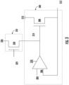
- an example supply voltage independent voltage regulator disable circuit 220 is provided. As shown in FIG. 2 , the example supply voltage independent voltage regulator disable circuit 220 supplies a regulator gate voltage 214 to an electrically connected voltage regulator 200, the voltage regulator 200 further configured to receive a reference voltage 204.
- the regulator gate voltage 214 is supplied by a power-down switching device 222 electrically connected to the voltage regulator 200.
- the power-down switching device 222 is configured to output the regulator gate voltage 214 based on a power-down output signal 224 and a selected voltage 226 supplied by an electrically connected voltage selection circuit 228.
- the voltage selection circuit 228 is configured to select the selected voltage 226 based on output voltages received from an electrically connected high voltage source 210 and an electrically connected low voltage source 212.
- the supply voltage independent voltage regulator disable circuit 220 supplies a regulator gate voltage 214 to a voltage regulator 200.
- the voltage regulator 200 may be any electronic component or device comprising hardware, firmware, software, or a combination thereof and configured to receive a reference voltage 204 and output a stable, consistent voltage within a specified range based on the reference voltage 204.
- the voltage regulator 200 may comprise a linear regulator, a switch regulator, a low-dropout regulator, a fixed voltage regulator, an adjustable voltage regulator, or similar type regulator.
- the voltage regulator 200 may be controlled by a regulator gate voltage 214.
- the switch device In an instance in which the regulator gate voltage 214 is at or near the voltage at the source terminal of the internal switch device (e.g., power MOSFET 108), the switch device is turned off and the output voltage from the voltage regulator 200 is stopped. Conversely, in an instance in which the regulator gate voltage 214 creates a voltage difference between the gate terminal and the source terminal of the switch device, the voltage regulator 200 is turned on and an output voltage from the voltage regulator 200 is generated.
- the internal switch device e.g., power MOSFET 108
- the supply voltage independent voltage regulator disable circuit 220 comprises a power-down switching device 222.
- a power-down switching device 222 may be any electrical component, plurality of components, or device, configured to control the passage of the selected voltage 226 from the voltage selection circuit 228 to the voltage regulator 200.
- the power-down switching device 222 may comprise a MOSFET, a bipolar junction transistor (BJT), a switch, or other switching device.
- the power-down switching device 222 may be a short, or resistor, allowing the selected voltage 226 or a portion of the selected voltage 226 to pass without switching.
- An example power-down switching device 222 is further provided in FIG. 3 .
- the power-down switching device 222 may be enabled by a power-down output signal 224.
- a power-down output signal 224 may be any electrical signal or series of signals providing indication to disable the voltage regulator 200.
- a power-down output signal 224 may be asserted when the voltage regulator 200 is to be powered down.
- the voltage of the power-down output signal 224 may be elevated above a pre-determined minimum voltage to indicate power down.
- the voltage of the power-down output signal 224 may be dropped below a pre-determined maximum voltage to indicate power down.
- the voltage of the power-down output signal 224 may be altered by a power-down generator circuit (as described in relation to FIG. 3 ) to protect the electrical components comprising the power-down switching device 222, and other electrical components, from exposure to high voltages exceeding the maximum voltage rating of the underlying semiconductor technology.
- the supply voltage independent voltage regulator disable circuit 220 further comprises a voltage selection circuit 228.
- a voltage selection circuit 228 may be any electrical components, including hardware, firmware, software, or any combination thereof configured to determine a selected voltage 226 based at least in part on the higher voltage between the high voltage source 210 and the low voltage source 212.
- an external low voltage source 212 may supply the low voltage within an electronic device.
- the internal voltage regulator 200 responsible for providing a low voltage source to the electronic device may be disabled.
- the high voltage source 210 may output a high voltage, no voltage, or any voltage in between.
- the voltage selection circuit 228 may not simply provide a selected voltage 226 equal to the high voltage source 210 but may select the selected voltage 226 based on the greater of the high voltage source 210 and the low voltage source 212. Example embodiments of the voltage selection circuit 228 are described in further detail in relation to FIG. 4 and FIG. 6 .
- an example power-down switching device 322 component of a supply voltage independent voltage regulator disable circuit (e.g., supply voltage independent voltage regulator disable circuit 220) is provided.
- the example power-down switching device 322 comprises a pull-up transistor 330 (e.g., pull-up switching component).
- the pull-up transistor 330 is electrically connected to the selected voltage 326 output of a voltage selection circuit (e.g., voltage selection circuit 228 as depicted in FIG. 2 ) at the source terminal and the regulator gate voltage 314 of the voltage regulator 300 at the drain terminal.
- the pull-up transistor 330 depicted in FIG. 3 is electrically connected to a power-down output signal 324 at the gate terminal of the pull-up transistor 330.
- the example power-down switching device 322 includes a pull-up transistor 330.
- a pull-up switching component may be any transistor, MOSFET, BJT, or other switching device that enables control of the regulator gate voltage 314 based on the selected voltage 326 and the power-down output signal 324.
- the pull-up transistor 330 enables the selected voltage 326 to be applied at the gate of the voltage regulator transistor 308 of the voltage regulator 300, thus disabling the flow of current through the voltage regulator transistor 308.
- the high voltage source 310 may be high (e.g., between 1.8 volts and 3.6 volts) when the power-down output signal 324 is asserted.
- the pull-up transistor 330 is enabled and the flow of current through the pull-up transistor 330 increases the regulator gate voltage 314 to the selected voltage 326, which is equivalent to the voltage (high voltage source 310) at the source of the voltage regulator transistor 308.
- the high voltage source 310 may be low (e.g., at or near 0 volts) when the power-down output signal 324 is asserted.
- the pull-up transistor 330 is enabled and the flow of current through the pull-up transistor 330 increases the regulator gate voltage 314 to the selected voltage 326, which is equivalent to the voltage (low voltage source 312) at the drain of the voltage regulator transistor 308.
- the flow of current at the voltage regulator transistor 308 is disabled and current flow from the low voltage source 312 to the high voltage source 310 through the voltage regulator transistor 308 is prevented.
- an example supply voltage independent voltage regulator disable circuit 440 is provided. As depicted in FIG. 4 , the example supply voltage independent voltage regulator disable circuit 440 includes a voltage selection circuit 428 electrically connected to a high voltage source 410 and a low voltage source 412 and generating a selected voltage 426 based on the high voltage source 410 and the low voltage source 412. In addition, the example supply voltage independent voltage regulator disable circuit 440 includes a power-down switching device 422 receiving the selected voltage 426 from the electrically connected voltage selection circuit 428 and further receiving a power-down output signal 424 from an electrically connected power-down generator circuit 442. As depicted in FIG.
- the power-down generator circuit 442 is electrically connected to the high voltage source 410 and is further configured to receive a power-down signal 444. As further depicted in FIG. 4 , the power-down switching device 422 is configured to generate a regulator gate voltage 414 supplied to an electrically connected voltage regulator 400.
- the example supply voltage independent voltage regulator disable circuit 440 includes a power-down generator circuit 442 configured to receive a power-down signal 444.
- a power-down generator circuit 442 may be any hardware, firmware, software, or combination thereof configured to receive a power-down signal 444 and apply necessary adjustments to the power-down signal 444 to avoid damage to electrical components due to high voltages.
- a power-down signal 444 may be any signal or sequence of signals providing an indication to power-down one or more electrically connected components, such as voltage regulator 400.
- the electrical components of the supply voltage independent voltage regulator disable circuit 440 may support a maximum voltage of 1.8 volts.
- the high voltage source is greater than 1.8 volts, for example 3.6 volts
- some electrical components may be exposed to a voltage difference greater than the maximum 1.8 volts.
- a power-down switching device 422 may comprise one or more transistors (e.g., pull-up transistor 330 as depicted in FIG. 3 ) having a maximum voltage rating of 1.8 volts.
- the power-down generator circuit 442 may adjust the power-down signal 444 to avoid exceeding the maximum voltage rating of the electrical components of the supply voltage independent voltage regulator disable circuit 440, the voltage regulator 400, and other electrically connected components.
- the example voltage selection circuit 528 includes a first transistor 550 (e.g., first transistor component) and a second transistor 551 (e.g., second transistor component) wherein the source terminal 550a, 551a of each transistor 550, 551 are electrically connected to the high voltage source 510.
- a first transistor 550 e.g., first transistor component
- a second transistor 551 e.g., second transistor component
- a first voltage divider 557 (e.g., first voltage selection circuit voltage divider) having a first resistor 552, a second resistor 553, and a first voltage divider tap 556 (e.g., first voltage divided output) electrically connected to the first voltage divider 557 between the first resistor 552 and the second resistor 553 is electrically connected between the drain terminal 550c of the first transistor 550 and the low voltage source 512.
- the drain terminal 550c of the first transistor 550 is electrically connected to the gate terminal 550b of the first transistor 550.
- the first voltage divider tap 556 is electrically connected to the gate terminal 551b of the second transistor 551.
- a second voltage divider 558 (e.g., second voltage selection circuit voltage divider) having a first resistor 554 (e.g., second voltage selection circuit voltage divider first resistive component), a second resistor 555 (e.g., second voltage selection circuit voltage divider second resistive component), and a second voltage divider tap 559 (e.g., second voltage circuit voltage divider tap) electrically connected to the second voltage divider 558 between the first resistor 554 and the second resistor 555 is electrically connected between the drain terminal 551c of the second transistor 551 and ground.
- the low voltage source 512 is electrically connected to the second voltage divider tap 559.
- the selected voltage 526 output is supplied by making an electrical connection at the drain terminal 551c of the second transistor 551.
- the example voltage selection circuit 528 includes a first transistor 550.
- the first transistor 550 may be any transistor, MOSFET, BJT, or other switching device that prevents the flow of current from the low voltage source 512 to the high voltage source 510 when a voltage from the low voltage source 512 is present and a voltage from the high voltage source 510 is not.
- the voltage at the gate terminal 550b is equivalent to the voltage at the drain terminal 550c (e.g., at or near the voltage of the low voltage source 512) and greater than the voltage at the source terminal 550a (e.g., approximately 0 volts), thus the first transistor 550 is disabled.
- the voltage at the source terminal 550a of the first transistor 550 is higher than the voltage at the gate terminal 550b of the first transistor 550 and the first transistor 550 is turned on. In such an instance, a voltage drop exists across the first transistor 550 and the first voltage divider 557 as described further herein.
- the example voltage selection circuit 528 includes a first voltage divider 557 electrically connected between the drain terminal 551c of the first transistor 550 and the low voltage source 512.
- a voltage divider 557 may be any hardware, firmware, software, or combination thereof configured to provide a reduced voltage level based on the voltage drop across the voltage divider 557.
- the first voltage divider 557 comprises a plurality of resistors (e.g., first resistor 552 and second resistor 553) connected in series.
- the first voltage divider 557 further includes a tap output provided by supplying an electrical contact to a point between the two resistors (e.g., first voltage divider tap 556).
- the voltage at the first voltage divider tap 556 may be determined based on the value of the two resistors and the voltage drop across the voltage divider 557.
- a reduced voltage level is generated at the first voltage divider tap 556 based on the resistance values of first resistor 552 and second resistor 553 and provided to the gate terminal 551b of the second transistor 551.
- the second resistor 553 may have a resistance of 75000 ohms, while the first resistor 552 may have a resistance of 5000 ohms.
- the example voltage selection circuit 528 includes a second transistor 551.
- the second transistor 551 may be any transistor, MOSFET, BJT, or other switching device that allows the flow of current through when the voltage at high voltage source 510 is high and prevents the flow of current in an instance in which the high voltage source is low.
- the voltage received from the first voltage divider tap 556 will be sufficiently lower than the high voltage source 510 at the gate terminal 551b of the second transistor 551, such that the second transistor 551 will be enabled and the selected voltage will be at or near the voltage of the high voltage source 510.
- the second transistor 551 will be off, or disabled, such that the selected voltage 526 is at or near the voltage of the low voltage source 512.
- the first transistor 550 and the second transistor 551 utilize fully depleted silicon-on-insulator (FDSOI) technology.
- FDSOI technology enables adjustments to the threshold voltage of a transistor to be made by applying a bias voltage to the bulk terminal (e.g., bulk terminal 550d, bulk terminal 551d) of the transistor.
- a bias voltage e.g., bulk terminal 550d, bulk terminal 551d
- increasing the voltage applied to the bulk terminal may increase the threshold voltage.
- n-type MOSFET transistors increasing the voltage applied to the bulk terminal may decrease the threshold voltage.
- electrically connecting the bulk terminal of the p-type MOSFETs to ground decreases the threshold voltage. As shown in FIG.
- the bulk terminal 550d of first transistor 550 is electrically connected to the high voltage source 510, thus increasing the threshold voltage of first transistor 550 and the bulk terminal 551d of second transistor 551 is electrically connected to ground, thus decreasing the threshold voltage of second transistor 551. Biasing first transistor 550 and second transistor 551 in this way ensures the second transistor 551 is strongly on when the high voltage source 510 is high.
- both the first transistor 550 and the second transistor 551 may comprise p-type transistors.
- the example voltage selection circuit 528 includes a second voltage divider 558 electrically connected between the drain terminal 551c of the second transistor 551 and ground.
- the second voltage divider 558 may be any hardware, firmware, software, or combination thereof configured to prevent the flow of current from the high voltage source 510 to the low voltage source 512 in an instance in which the high voltage source 510 is high and the regulator is disabled, such that the low voltage source 512 is low.
- the second voltage divider 558 comprises a plurality of resistors (e.g., first resistor 554 and second resistor 555) connected in series.
- the second voltage divider 558 further includes a tap output provided by supplying an electrical contact to a point between the two resistors (e.g., second voltage divider tap 559).
- the resistance value of second resistor 555 may be much less than the resistance value of the first resistor 554.
- the second resistor 555 may have a resistance of 180 ohms, while the first resistor 554 may have a resistance of 200000 ohms.
- the low voltage source 512 may be kept close to ground in an instance in which the low voltage source 512 is not provided, and may be protected from receiving charge from the high voltage source 510 when the second transistor 551 is enabled.
- the example voltage selection circuit 528 may enable the use of voltages greater than the maximum tolerable voltage difference across two terminals of the underlying electrical components. For example, in an instance in which the maximum tolerable voltage difference across two terminals of the first transistor 550 and the second transistor 551 is 1.8 volts, and the high voltage source 510 is 3.6 volts, the transistors may be protected from a voltage difference of more than 1.8 volts at any of the terminals.
- the first voltage divider 557 ensures that the voltage at the drain terminal 550c and thus the gate terminal 550b is at or near 3.6 volts, thus, none of the terminals on the first voltage divider 557 exceed the maximum tolerable voltage difference across two terminals.
- the second resistor 553 is greater than the first resistor 552
- the first voltage divider tap 556 supplied to the gate terminal 551b of the gate terminal is sufficiently close to the high voltage source 510 as to not exceed the maximum tolerable voltage difference across two terminals of the second transistor 551.
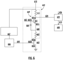
- the example power-down generator circuit 642 includes a voltage divider 669 (e.g., power-down voltage divider) comprising a first resistor 660 (e.g., power-down voltage divider first resistive component), a second resistor 662 (e.g., power-down voltage divider second resistive component), and a tap 668 (e.g., power-down voltage divider tap).
- a voltage divider 669 e.g., power-down voltage divider
- first resistor 660 e.g., power-down voltage divider first resistive component
- second resistor 662 e.g., power-down voltage divider second resistive component
- a tap 668 e.g., power-down voltage divider tap
- the example power-down generator circuit 642 includes a first transistor 661 (e.g., first power-down transistor component) electrically connected to the first resistor 660 at the drain terminal 661a and the second resistor 662 at the source terminal 661c.
- the power-down generator circuit 642 further comprises a conductive path diode 664 electrically connected at the anode end to the source terminal 661c of the first transistor 661, and electrically connected at the cathode end to the gate terminal 661b of the first transistor 661.
- a floating voltage supply 665 is electrically connected to the gate terminal 661b of the first transistor 661. As further depicted in FIG.
- a second transistor 663 (e.g., second power-down transistor component) is electrically connected between the second resistor 662 and ground. Further, a power-down signal 644 is electrically connected to the gate terminal 663b of the second transistor 663 as provided by electrically connected logic circuitry 666 and an electrically connected internal supply generator 667. Further depicted in FIG. 6 , the high voltage source 610 is electrically connected to the first resistor 660 of the voltage divider 669, and the power-down output signal 624 is provided to the power-down switching device 622 through an electrical connection to the drain terminal 661a of the first transistor 661.
- the high voltage source 610 is electrically connected to the first resistor 660 of the voltage divider 669
- the power-down output signal 624 is provided to the power-down switching device 622 through an electrical connection to the drain terminal 661a of the first transistor 661.
- the power-down generator circuit 642 receives a power-down signal 644 from logic circuitry 666 located on or near an electronic device utilizing the high voltage source 610.
- the logic circuitry 666 receives a power supply from an internal supply generator 667 that may be a reduced voltage from the high voltage source 610.
- the high voltage source may be 3.6 volts, while the power supply provided to the logic circuitry 666 by the internal supply generator is only 1.8 volts.
- the logic circuitry 666 may be configured to generate a power-down signal 644 providing an indication to power-down the voltage regulator 600.
- the logic circuitry 666 may assert, or raise the voltage of the power-down signal 644 to initiate the power-down of the voltage regulator 600, and de-assert, or set the voltage of the power-down signal 644 to 0 volts, to enable the voltage regulator 600.
- the power-down signal 644 may operate in the reduced voltage range provided by the internal supply generator 667 (e.g., 0 to 1.8 volts). In such an instance, the power-down generator circuit 642 may alter the signal to prevent exceeding the maximum tolerable voltage difference across two terminals of any electrical devices when the high voltage source 610 is in excess of the maximum tolerable voltage difference across two terminals of the electrical components.
- the power-down generator circuit 642 may shift the power domain of the power-down signal 644 to be equivalent to the high voltage source 610 when the voltage regulator 600 is to be disabled, and half of the high voltage source 610 when the voltage regulator 600 is to be enabled.
- the power-down generator circuit 642 includes a voltage divider 669 comprising a first resistor 660 and a second resistor 662.
- the first resistor 660 and the second resistor 662 create a voltage divider from which the power-down output signal 624 is generated.
- the first resistor 660 and the second resistor 662 may be nearly equivalent.
- the voltage at the tap 668 is half the value of the high voltage source 610 when the opposite end of the voltage divider 669 is electrically connected to ground.
- the voltage divider 669 is essentially enabled by the power-down signal 644 at the second transistor 663. As shown in FIG.
- the second transistor 663 is an n-type transistor and is electrically connected between the second resistor 662 of the voltage divider 669 and ground.
- the power-down signal 644 is low (e.g., 0 volts)
- the second transistor 663 is turned off, and the voltage at the high voltage source 610 is output as the power-down output signal 624.
- the power-down output signal 624 and the selected voltage 626 are both essentially equal to the high voltage source 610 and the power-down switching device 622 is disabled, allowing the voltage regulator 600 to continue to operate.
- the second transistor 663 is turned on, thus, the voltage divider 669 is connected to ground and the voltage divider 669 activated.
- the power-down output signal 624 is equivalent to approximately one-half of the high voltage source 610, while the selected voltage 626 remains at the high voltage source 610.
- the power-down switching device 622 is enabled, the high voltage source 610 is transmitted through the power-down switching device 622 as the regulator gate voltage 614, and the voltage regulator 600 is disabled.
- the power-down generator circuit 642 includes a first transistor 661 electrically connected to the first resistor 660 at the drain terminal 661a, to the second resistor 662 at the source terminal 661c, and to the floating voltage supply 665 at the gate terminal 661b.
- the electrical components may be damaged if the voltage difference across the component is greater than the maximum tolerable voltage difference across two terminals of the component.
- the second transistor 663 may be damaged.
- the purpose of the first transistor 661 may be to protect the second transistor 663 from such a situation.
- the gate terminal 661b of the first transistor 661 is electrically connected to a floating voltage supply 665.
- the floating voltage supply 665 depicted in FIG. 6 generates a bias voltage based on the voltage of the high voltage source 610.
- the floating voltage supply 665 In an instance in which the high voltage source 610 exceeds a voltage threshold (e.g., 2 volts), the floating voltage supply 665 generates a voltage equivalent to one-half of the high voltage source 610. However, when the high voltage source 610 is less than or equal to the voltage threshold, the floating voltage supply 665 generates a voltage equivalent to the high voltage source. Thus, by biasing the voltage at the gate terminal 661b of the first transistor 661 according to the floating voltage supply 665, the voltage at the tap 668 and the source of the second transistor 663 may be held below the maximum tolerable voltage difference across two terminals of the second transistor 663.
- a voltage threshold e.g. 2 volts
- both the first transistor 661 and the second transistor 663 may comprise n-type transistors.
- the example power-down generator circuit 642 includes a conductive path diode 664 with the anode electrically connected to the source terminal 661c of the first transistor 661, and the cathode electrically connected to the gate terminal 661b of the first transistor 661.
- a conductive path diode 664 may be any electronic device that allows the flow in only one direction, from the anode to the cathode.
- the conductive path diode 664 further protects the second transistor 663 by preventing any increase in voltage above the bias voltage of the floating voltage supply 665 at the tap 668 and/or source terminal 663a of the second transistor 663 due to leakage or other factors.
- a voltage selection circuit 728 of a supply voltage independent voltage regulator disable circuit is provided.
- the voltage selection circuit 728 is designed using transistors without FDSOI technology.
- the bulk terminal 771d of the second transistor 771 is electrically connected to the selected voltage 726
- the bulk terminals 770d, 772d of the first and third transistors 770, 772 are electrically connected to the selected voltage 726, since the bulk terminal of a non-FDSOI transistor may not be lower than the voltage of the source terminal or the drain terminal on the non-FDSOI transistor.
- an additional transistor (third transistor 773) is added to create an additional voltage drop from the high voltage source 710 across the first transistor 770 and the third transistor 772, such that the total voltage drop across the first transistor 770 and the third transistor 772 is sufficiently greater than the required threshold voltage of the second transistor 771.
- the example voltage selection circuit 728 includes a first transistor 770 electrically connected in series with a third transistor 772 and a first resistor 773 between the high voltage source 710 and the low voltage source 712.
- the source terminal 770a of the first transistor 770 is electrically connected to high voltage source 710
- the gate terminal 770b is electrically connected to the drain terminal 770c
- the bulk terminal 770d is electrically connected to the selected voltage 726.
- the source terminal 772a of the third transistor 772 is electrically connected to the drain terminal 770c of the first transistor 770
- the gate terminal 772b is electrically connected to the drain terminal 772c
- the drain terminal 772c is further electrically connected to the first resistor 773
- the bulk terminal 772d is electrically connected to the selected voltage 726.
- the first resistor 773 is further electrically connected to the low voltage source 712.
- the voltage selection circuit 728 further includes a second transistor 771 electrically connected in series with a second resistor 774, and a third resistor 775 between the high voltage source 710 and low voltage source 712, and in parallel to the first transistor 770, third transistor 772, and first resistor 773, wherein the voltage at the gate terminal 771b of the second transistor 771 is supplied by the voltage at the drain terminal 772c of the third transistor 772.
- the source terminal 771a of the second transistor 771 is electrically connected to the high voltage source 710
- the gate terminal 771b is electrically connected to the drain terminal 772c of the third transistor 772
- the drain terminal 771c is electrically connected to the second resistor 774
- the bulk terminal 771d is electrically connected to the selected voltage 726.
- the second resistor 774 is further electrically connected to the third resistor 775.
- the selected voltage is generated at the drain terminal 771c of the second transistor 771.
- the first transistor 770, the third transistor 772, and the first resistor 773 essentially act as a voltage divider with a voltage divider tap 756 generating the output voltage used to control the second transistor 771. Due to the lack of FDSOI technology, there is less flexibility in control of the threshold voltage using the bulk terminal. Thus, the additional transistor (third transistor 772) is added to ensure the voltage difference between the gate terminal 771b and the source terminal 771a at second transistor 771 is high enough to reduce the effective resistance of the second transistor 771.
- the bulk terminals of the transistors (770d, 771d, 772d) are electrically connected to the selected voltage 726. Connecting the bulk terminals to the selected voltage 726 biases the bulk terminal to avoid forward bias of the transistors, for example, when a voltage is present at low voltage source 712 and not at high voltage source 710.
- any transistor connected to the gate terminal of a transistor may be connected to the selected voltage 726.
- the bulk terminal of any transistor connected to the gate terminal may be connected to selected voltage 726.
- an example voltage regulator 800 and associated example power-down switching device 822 are depicted.
- the gate terminal of the power MOSFET 808 of the example voltage regulator 800 receives a regulator gate voltage 814 based on the selected voltage 826 and the power-down output signal 824 as received by the power-down switching device 822.
- any transistor connected to the gate terminal of the power MOSFET 808 may receive the selected voltage 826 at the bulk terminal of the transistor.
- the last stage of the operational amplifier 802 may comprise one or more transistors. As shown, the transistors within the last stage of the operational amplifier 802 are powered by the high voltage source 810 and thus may additionally receive the selected voltage 826 at the bulk terminals of the transistors.
- an example power management unit (PMU) 990 comprising a voltage regulator 900 disabled by a regulator gate voltage 914 according to one or more embodiments of the present disclosure is provided.
- the example PMU 990 includes a transformer 992 which may be configured to receive an alternating current (AC) power source 991 and transfer the received electrical energy at the proper voltage level to the rectifier 994.
- the rectifier 994 may be configured to receive the altered AC power from the transformer 992 and convert the AC power into direct current (DC) power usable by the electronic circuit.
- DC direct current
- the PMU 990 may further include a filter 996 configured to receive DC power from the rectifier 994 and generate a clean (noise reduced) DC power source to be transmitted to the voltage regulator 900.
- the voltage regulator 900 may receive a DC voltage from the filter 996 as a reference voltage (e.g., reference voltage 104).
- the voltage regulator 900 ensures that the DC voltage supplied to the electrical circuit remains stable, despite fluctuations in the AC power source 991.
- the voltage regulator 900 may receive a power-down signal (e.g., regulator gate voltage 914, used to shut off the voltage regulator 900, for example, in an instance in which the low voltage supply is supplied by an external source.
- the voltage output of the voltage regulator 900 is transmitted to a voltage divider 998.
- the voltage divider 998 may be configured to generate one or more lower voltages based on the voltage generated by the voltage regulator 900.
- the output DC power 999 of the voltage divider 998 may be utilized as a power source to various electrical components of an electrical device, processor, core logic of a system-on-chip, or other electrical components.
Landscapes
- Engineering & Computer Science (AREA)
- Power Engineering (AREA)
- Physics & Mathematics (AREA)
- Electromagnetism (AREA)
- General Physics & Mathematics (AREA)
- Radar, Positioning & Navigation (AREA)
- Automation & Control Theory (AREA)
- Theoretical Computer Science (AREA)
- General Engineering & Computer Science (AREA)
- Continuous-Control Power Sources That Use Transistors (AREA)
Abstract
Description
- The present disclosure relates generally to disabling voltage regulators in a power management unit (PMU) of a system-on-chip (SoC), and more particularly, to circuitry for disabling a voltage regulator independent of the supply voltage sequence and tolerant to high voltages.
- Various examples address technical problems associated with disabling a voltage regulator, independent of control over the input power supplies and tolerant to high voltages. As understood by those of skill in the field to which the present disclosure pertains, there are numerous example scenarios in which a user may need to disable a voltage regulator independent of the supply of voltage received at the voltage regulator.
- For example, a power management unit (PMU) is generally responsible for providing a stable source of power to a system-on-chip (SoC) electronic device. Many regulators may support multiple power domains, for example, a regulator may provide both a low voltage supply and a high voltage supply depending on the supplied power. In general, the PMU generates a low voltage power supply to be supplied to the core logic of the SoC. However, in some instances, the low voltage power supply may be provided by an external power supply. When the low voltage supply is supplied externally, the voltage regulator should be disabled. In an instance in which power is supplied by an external power supply, the change in power supplies may not be synchronized, potentially leading to undesirable electrical flow conditions.
- Applicant has identified many technical challenges and difficulties associated with disabling a voltage regulator independent of supply voltages. Through applied effort, ingenuity, and innovation, Applicant has solved problems related to disabling voltage regulators by developing solutions embodied in the present disclosure, which are described in detail below.
- Various embodiments are directed to an example circuit, and power management unit utilizing the example circuit to disable a voltage regulator. In some embodiments, the example circuit may comprise a voltage selection circuit configured to receive a first voltage source and a second voltage source, and further configured to output a selected voltage. In some embodiments, the voltage selection circuit may comprise a first transistor component having a first transistor component source, a first transistor component gate, and a first transistor component drain, wherein the first transistor component source is electrically connected to the first voltage source, and wherein the first transistor component gate is electrically connected to the first transistor component drain. In some embodiments, the voltage selection circuit may further comprise a second transistor component having a second transistor component source, a second transistor component gate, and a second transistor component drain, wherein the second transistor component source is electrically connected to the first voltage source, and wherein a second transistor gate voltage at the second transistor component gate is generated based at least in part on a first transistor component drain voltage at the first transistor component drain. In some embodiments, the selected voltage is generated based at least in part on a second transistor drain voltage at the second transistor component drain. The electrical circuit may further comprise a power-down switching device configured to generate a regulator gate voltage for a voltage regulator based at least in part on the selected voltage.
- In some embodiments, the power-down switching device may further comprise a pull-up switching component having a pull-up transistor source, a pull-up transistor gate, and a pull-up transistor drain, wherein the pull-up transistor source is electrically connected to the selected voltage of the voltage selection circuit, and wherein the pull-up transistor gate is electrically connected to a power-down output signal of a power-down generator circuit.
- In some embodiments, the power-down generator circuit may be configured to receive the first voltage source and a power-down signal, wherein the power-down generator circuit further comprises a power-down voltage divider electrically connected to the first voltage source and the power-down signal, wherein the power-down voltage divider is enabled by the power-down signal, and wherein the power-down voltage divider generates the power-down output signal based at least in part on a voltage difference between the first voltage source and the power-down signal.
- In some embodiments, the voltage selection circuit further comprises a first voltage selection circuit voltage divider electrically connected to the first transistor component drain of the first transistor component and the second voltage source, wherein the first voltage selection circuit voltage divider is configured to generate a first voltage divided output based on a voltage difference between the first transistor component drain voltage at the first transistor component drain and the second voltage source. In some embodiments, the first voltage divided output may be electrically connected to the second transistor component gate of the second transistor component.
- In some embodiments, the voltage selection circuit may further comprise a second voltage selection circuit voltage divider electrically connected to the selected voltage and a ground, wherein a second voltage selection circuit voltage divider tap is electrically connected to the second voltage source.
- In some embodiments, the second voltage selection circuit voltage divider may comprise a second voltage selection circuit voltage divider first resistive component electrically connected to the selected voltage and the second voltage selection circuit voltage divider, the second voltage selection circuit voltage divider tap, and a second voltage selection circuit voltage divider second resistive component electrically connected to the ground and the second voltage selection circuit voltage divider tap. In some embodiments, a resistive value of the second voltage selection circuit voltage divider first resistive component may be greater than the resistive value of the second voltage selection circuit voltage divider second resistive component.
- In some embodiments, the power-down voltage divider may comprise a power-down voltage divider first resistive component electrically connected to the first voltage source and the power-down output signal, a power-down voltage divider tap electrically connected to the power-down output signal; and a power-down voltage divider second resistive component electrically connected to the power-down voltage divider tap and the power-down signal.
- In some embodiments, the power-down voltage divider further comprises a first power-down transistor component having a first power-down transistor component source, a first power-down transistor component gate, and a first power-down transistor component drain. In some embodiments, the first power-down transistor component drain is electrically connected to the power-down voltage divider tap, the first power-down transistor component source is electrically connected to the power-down voltage divider second resistive component, and the first power-down transistor component gate, and wherein the first power-down transistor component gate is further connected to a floating voltage supply block.
- In some embodiments, the power-down voltage divider further comprises a second power-down transistor component having a second power-down transistor component source, a second power-down transistor component gate, and a second power-down transistor component drain. In some embodiments, the second power-down transistor component drain is electrically connected to the power-down voltage divider second resistive component, the second power-down transistor component gate is electrically connected to the power-down signal, and the second power-down transistor component source is electrically connected to ground.
- In some embodiments, a conductive path diode may be electrically connected between the power-down voltage divider tap and the first power-down transistor component gate.
- In some embodiments, the floating voltage supply block may generate a floating supply voltage based on a voltage output of the first voltage source.
- In some embodiments, the first transistor component and the second transistor component may be p-type metal-oxide-semiconductor field-effect transistors.
- In some embodiments, the first power-down transistor component and the second power-down transistor component may be n-type metal-oxide-semiconductor field-effect transistors.
- In some embodiments, the voltage regulator may comprise an operational amplifier having a first input and a second input, wherein the first input is electrically connected to a reference voltage. In some embodiments, the voltage regulator may further comprise a voltage regulator transistor component having a voltage regulator transistor component source, a voltage regulator transistor component gate, and a voltage regulator transistor component drain.
- In some embodiments, the voltage regulator transistor component source may be electrically connected to an output of the operational amplifier, the voltage regulator transistor component gate may be electrically connected to an output of the operational amplifier and to the regulator gate voltage; and the voltage regulator transistor component drain may be electrically connected to the second input of the operational amplifier.
- In some embodiments an example power management unit utilizing an example circuit to disable a voltage regulator is further provided. In some embodiments, the example power management unit may comprise a transformer, a rectifier circuit electrically connected to the transformer, a filter circuit electrically connected to the rectifier circuit, and a voltage regulator. In some embodiments, the voltage regulator may comprise a voltage selection circuit configured to receive a first voltage source and a second voltage source, and further configured to output a selected voltage. In some embodiments, the voltage selection circuit may comprise a first transistor component having a first transistor component source, a first transistor component gate, and a first transistor component drain, wherein the first transistor component source is electrically connected to the first voltage source, and wherein the first transistor component gate is electrically connected to the first transistor component drain. In some embodiments, the voltage selection circuit may further comprise a second transistor component having a second transistor component source, a second transistor component gate, and a second transistor component drain. In some embodiments, the second transistor component source may be electrically connected to the first voltage source, and a second transistor component gate voltage at the second transistor component gate may be generated based at least in part on a first transistor component drain voltage at the first transistor drain. In some embodiments, the selected voltage may be generated based at least in part on a second transistor component drain voltage at the second transistor component drain. In some embodiments, the voltage regulator may further comprise a power-down switching device configured to generate a regulator gate voltage for the voltage regulator based at least in part on the selected voltage. In some embodiments, the voltage regulator may further comprise an operational amplifier having a first input and a second input, wherein the first input may be electrically connected to a reference voltage. In some embodiments, the voltage regulator may further comprise a voltage regulator transistor component having a voltage regulator transistor component source, a voltage regulator transistor component gate, and a voltage regulator transistor component drain. In some embodiments, the voltage regulator transistor component source may be electrically connected to an output of the operational amplifier, the voltage regulator transistor component gate may be electrically connected to an output of the operational amplifier and to the regulator gate voltage, and the voltage regulator transistor component drain may be electrically connected to the second input of the operational amplifier.
- In some embodiments, the power-down switching device may further comprise a pull-up switching component having a pull-up transistor source, a pull-up transistor gate, and a pull-up transistor drain. In some embodiments, the pull-up transistor source may be electrically connected to the selected voltage of the voltage selection circuit, and the pull-up transistor gate may be electrically connected to a power-down output signal of a power-down generator circuit.
- In some embodiments, the power-down generator circuit may be configured to receive the first voltage source and a power-down signal, wherein the power-down generator circuit further comprises a power-down voltage divider electrically connected to the first voltage source and the power-down signal. In some embodiments, the power-down voltage divider may be enabled by the power-down signal, and the power-down voltage divider may generate the power-down output signal based at least in part on a voltage difference between the first voltage source and the power-down signal.
- In some embodiments, the voltage selection circuit may further comprise a first voltage selection circuit voltage divider electrically connected to the first transistor component drain of the first transistor component and the second voltage source. In some embodiments, the first voltage selection circuit voltage divider may be configured to generate a first voltage divided output based on a voltage difference between the first transistor component drain voltage at the first transistor component drain and the second voltage source, and the first voltage divided output may be electrically connected to the second transistor component gate of the second transistor component.
- In some embodiments, the voltage selection circuit may further comprise a second voltage selection circuit voltage divider electrically connected to the selected voltage and a ground, wherein a second voltage selection circuit voltage divider tap is electrically connected to the second voltage source.
- Reference will now be made to the accompanying drawings. The components illustrated in the figures may or may not be present in certain embodiments described herein. Some embodiments may include fewer (or more) components than those shown in the figures in accordance with an example of the present disclosure.
-
FIG. 1 illustrates an example voltage regulator in accordance with an example of the present disclosure. -
FIG. 2 illustrates an example block diagram of an example supply voltage independent voltage regulator disable circuit in accordance with an example of the present disclosure. -
FIG. 3 illustrates an example embodiment of a power-down switching device interfacing with a voltage regulator in accordance with an example of the present disclosure. -
FIG. 4 illustrates an example block diagram of an example supply voltage independent voltage regulator disable circuit including an example power-down generator circuit in accordance with an example of the present disclosure. -
FIG. 5 illustrates an example of a voltage selection circuit in accordance with an example of the present disclosure. -
FIG. 6 illustrates an example of a power-down generator circuit in accordance with an example of the present disclosure. -
FIG. 7 illustrates an example of a voltage selection circuit utilizing bulk technology in accordance with an example of the present disclosure. -
FIG. 8 illustrates an example of a voltage regulator and power-down switching device utilizing bulk technology in accordance with an example of the present disclosure. -
FIG. 9 depicts a system-level block diagram of a PMU comprising a voltage regulator in accordance with an example of the present disclosure. - Example embodiments will be described more fully hereinafter with reference to the accompanying drawings, in which some, but not all embodiments of the inventions of the disclosure are shown. Indeed, embodiments of the disclosure may be embodied in many different forms and should not be construed as limited to the embodiments set forth herein; rather, these embodiments are provided so that this disclosure will satisfy applicable legal requirements. Like numbers refer to like elements throughout.
- As described herein, the term "high" when referring to voltages indicates the identified voltage is above a certain minimum voltage threshold for the electronic device, generally between 1.8 volts and 3.6 volts. Similarly, the term "low" when referring to voltages indicates the identified voltage is below a certain voltage threshold for the electronic device, generally at or near 0 volts.
- Various example embodiments address technical problems associated with disabling a voltage regulator, independent of synchronization with supply voltages. As understood by those of skill in the field to which the present disclosure pertains, there are numerous example scenarios in which a user may need to disable a voltage regulator independent of the supply of voltage received at the voltage regulator. For example, a power management unit (PMU) is generally responsible for providing a stable source of power to a system-on-chip (SoC) electronic device. Many regulators may support multiple power domains, for example, a regulator may provide both a low voltage supply and a high voltage supply depending on the supplied power. In addition, in some instances, an SoC or other electronic device may support an externally supplied voltage source. In an instance in which the power supply is provided by an external voltage regulator, one or more voltage regulators of the PMU may need to be disabled.
- Referring to
FIG, 1 , acommon voltage regulator 100 is provided. As shown inFIG. 1 , thecommon voltage regulator 100 comprises anop amp 102 having a first input terminal where areference voltage 104 is received, and asecond input terminal 106 configured to receive feedback from thedrain terminal 108c of an electrically connected transistor (e.g., power MOSFET 108). In some embodiments, the reference voltage may be supplied by a bandgap circuit and may comprise a voltage at or near 900 millivolts, however, areference voltage 104 may be received from any stable voltage source and may comprise a wide range of voltages. Theop amp 102 may further receive power from ahigh voltage source 110. In some embodiments, thehigh voltage source 110 may comprise a voltage in a range from 1.8 volts to 3.6 volts, however, ahigh voltage source 110 may comprise a wide range of voltages with a peak voltage greater than thelow voltage source 112. Theop amp 102 depicted inFIG. 1 , generates aregulator gate voltage 114 on an output. The output of theop amp 102 is electrically connected to a power metal-oxide-semiconductor field-effect-transistor (MOSFET) 108. - As shown in
FIG. 1 , thepower MOSFET 108 includes three terminals, asource terminal 108a, agate terminal 108b, and adrain terminal 108c. Thesource terminal 108a is the point at which, when enabled, current generally flows into thepower MOSFET 108. As depicted inFIG. 1 , thesource terminal 108a is electrically connected to thehigh voltage source 110. Thedrain terminal 108c is the point at which the current generally flows out of thepower MOSFET 108. As depicted inFIG. 1 , thedrain terminal 108c is electrically connected to thesecond input terminal 106 of theop amp 102. In addition, as depicted inFIG. 1 , thedrain terminal 108c of thepower MOSFET 108 supplies thelow voltage source 112 to the electrically connected device. - In general, the
gate terminal 108b of a MOSFET is used to control the flow of current between thesource terminal 108a and thedrain terminal 108c. In some embodiments, a gate terminal voltage at or near the voltage at thesource terminal 108a may be applied to turn off the MOSFET and stop the flow of current through the MOSFET. Conversely, a gate terminal voltage that creates a voltage difference between the gate terminal and the source terminal may turn on the MOSFET and allow the flow of current through the MOSFET. - When a power supply is supplied externally, a voltage regulator, for example the
voltage regulator 100 shown inFIG. 1 , may be disabled. For example, in an instance in which thevoltage regulator 100 supplies the low voltage power source to the electrically connected device, thevoltage regulator 100 may be disabled. However, because of the asynchronous nature of the external power source, thehigh voltage source 110 may be enabled and providing power at a voltage higher than thelow voltage source 112, or, alternatively, thehigh voltage source 110 may be disabled at a voltage at or near 0. - The state of the
high voltage source 110 when thevoltage regulator 100 is disabled is important in determining theregulator gate voltage 114 necessary to disable thepower MOSFET 108. For example, in an instance in which thehigh voltage source 110 is at 0 volts, if theregulator gate voltage 114 is pulled to thehigh voltage source 110 in an attempt to turn off the MOSFET, the voltage at thegate terminal 108b (0 volts) and at thesource terminal 108a (0 volts) are both lower than the voltage at thedrain terminal 108c. Thus, current may flow from thelow voltage source 112 into thehigh voltage source 110, which is undesirable. - In addition, in some embodiments, the maximum voltage rating of one or more of the electrical components may be less than the voltage provided by the
high voltage source 110. In such an embodiment, electrical components may be damaged or destroyed if the voltage drop across the component is greater than the maximum voltage rating. - The various example embodiments described herein utilize various techniques to ensure a voltage regulator is properly disabled in an instance in which the voltage source is provided by an external, asynchronous source. For example, in some embodiments, a voltage selection circuit is provided to generate a selected voltage that is the higher of the two supply voltages. In addition, the voltage selection circuit ensures that the voltage drop across the electrical components does not exceed the maximum voltage rating of the electrical components, for example, 1.8 volts.
- In some embodiments, a power-down generator circuit is further provided. In general, a power-down generator circuit may be configured to relay a power-down signal from the logic domain of the electronic device and enable the selected voltage supply to the voltage regulator. However, in some embodiments, the power-down signal may be adjusted based on the selected voltage. For example, in some embodiments, the selected voltage may be greater than the maximum voltage rating of the electrical components of a power-down switching device, such as a transistor. In such an embodiment, the power-down signal may be adjusted to prevent a voltage drop across the electrical components greater than the maximum voltage rating of the electrical components.
- As a result of the herein described example embodiments and in some examples, the performance of a voltage regulator may be greatly improved. In addition, electrical components having a maximum voltage rating lower than the voltage of a high voltage source may be utilized.
- Referring now to
FIG. 2 , an example supply voltage independent voltage regulator disablecircuit 220 is provided. As shown inFIG. 2 , the example supply voltage independent voltage regulator disablecircuit 220 supplies aregulator gate voltage 214 to an electrically connectedvoltage regulator 200, thevoltage regulator 200 further configured to receive areference voltage 204. Theregulator gate voltage 214 is supplied by a power-down switching device 222 electrically connected to thevoltage regulator 200. The power-down switching device 222 is configured to output theregulator gate voltage 214 based on a power-downoutput signal 224 and a selectedvoltage 226 supplied by an electrically connectedvoltage selection circuit 228. Thevoltage selection circuit 228 is configured to select the selectedvoltage 226 based on output voltages received from an electrically connectedhigh voltage source 210 and an electrically connectedlow voltage source 212. - As depicted in
FIG. 2 , the supply voltage independent voltage regulator disablecircuit 220 supplies aregulator gate voltage 214 to avoltage regulator 200. As described in relation toFIG. 1 , thevoltage regulator 200 may be any electronic component or device comprising hardware, firmware, software, or a combination thereof and configured to receive areference voltage 204 and output a stable, consistent voltage within a specified range based on thereference voltage 204. Thevoltage regulator 200 may comprise a linear regulator, a switch regulator, a low-dropout regulator, a fixed voltage regulator, an adjustable voltage regulator, or similar type regulator. As described in relation toFIG. 1 , thevoltage regulator 200 may be controlled by aregulator gate voltage 214. In an instance in which theregulator gate voltage 214 is at or near the voltage at the source terminal of the internal switch device (e.g., power MOSFET 108), the switch device is turned off and the output voltage from thevoltage regulator 200 is stopped. Conversely, in an instance in which theregulator gate voltage 214 creates a voltage difference between the gate terminal and the source terminal of the switch device, thevoltage regulator 200 is turned on and an output voltage from thevoltage regulator 200 is generated. - As further depicted in
FIG. 2 , the supply voltage independent voltage regulator disablecircuit 220 comprises a power-down switching device 222. A power-down switching device 222 may be any electrical component, plurality of components, or device, configured to control the passage of the selectedvoltage 226 from thevoltage selection circuit 228 to thevoltage regulator 200. In some embodiments, the power-down switching device 222 may comprise a MOSFET, a bipolar junction transistor (BJT), a switch, or other switching device. In some embodiments, the power-down switching device 222 may be a short, or resistor, allowing the selectedvoltage 226 or a portion of the selectedvoltage 226 to pass without switching. An example power-down switching device 222 is further provided inFIG. 3 . - In some embodiments, the power-
down switching device 222 may be enabled by a power-downoutput signal 224. A power-downoutput signal 224 may be any electrical signal or series of signals providing indication to disable thevoltage regulator 200. For example, a power-downoutput signal 224 may be asserted when thevoltage regulator 200 is to be powered down. In some embodiments, the voltage of the power-downoutput signal 224 may be elevated above a pre-determined minimum voltage to indicate power down. In some embodiments, the voltage of the power-downoutput signal 224 may be dropped below a pre-determined maximum voltage to indicate power down. In some embodiments, the voltage of the power-downoutput signal 224 may be altered by a power-down generator circuit (as described in relation toFIG. 3 ) to protect the electrical components comprising the power-down switching device 222, and other electrical components, from exposure to high voltages exceeding the maximum voltage rating of the underlying semiconductor technology. - As further depicted in
FIG. 2 , the supply voltage independent voltage regulator disablecircuit 220 further comprises avoltage selection circuit 228. Avoltage selection circuit 228 may be any electrical components, including hardware, firmware, software, or any combination thereof configured to determine a selectedvoltage 226 based at least in part on the higher voltage between thehigh voltage source 210 and thelow voltage source 212. In some embodiments, an externallow voltage source 212 may supply the low voltage within an electronic device. In an instance in which the low voltage is supplied by an externallow voltage source 212, theinternal voltage regulator 200 responsible for providing a low voltage source to the electronic device may be disabled. In such an embodiment, thehigh voltage source 210 may output a high voltage, no voltage, or any voltage in between. In an instance in which thelow voltage source 212 is provided but thehigh voltage source 210 is at or near 0 volts, disabling thevoltage regulator 200 by tying theregulator gate voltage 214 to thehigh voltage source 210 may result in a voltage at the drain terminal of the power MOSFET (e.g., power MOSFET 108) within thevoltage regulator 200 that is higher than the voltage at the gate terminal and the voltage at the source terminal. This scenario may result in current flowing from thelow voltage source 212 to thehigh voltage source 210, which may be undesirable. Thus, thevoltage selection circuit 228 may not simply provide a selectedvoltage 226 equal to thehigh voltage source 210 but may select the selectedvoltage 226 based on the greater of thehigh voltage source 210 and thelow voltage source 212. Example embodiments of thevoltage selection circuit 228 are described in further detail in relation toFIG. 4 andFIG. 6 . - Referring now to
FIG. 3 , an example power-down switching device 322 component of a supply voltage independent voltage regulator disable circuit (e.g., supply voltage independent voltage regulator disable circuit 220) is provided. As depicted inFIG. 3 , the example power-down switching device 322 comprises a pull-up transistor 330 (e.g., pull-up switching component). The pull-uptransistor 330 is electrically connected to the selectedvoltage 326 output of a voltage selection circuit (e.g.,voltage selection circuit 228 as depicted inFIG. 2 ) at the source terminal and theregulator gate voltage 314 of thevoltage regulator 300 at the drain terminal. In addition, the pull-uptransistor 330 depicted inFIG. 3 is electrically connected to a power-downoutput signal 324 at the gate terminal of the pull-uptransistor 330. - As depicted in
FIG. 3 , the example power-down switching device 322 includes a pull-uptransistor 330. Although depicted as a pull-uptransistor 330 inFIG. 3 , a pull-up switching component may be any transistor, MOSFET, BJT, or other switching device that enables control of theregulator gate voltage 314 based on the selectedvoltage 326 and the power-downoutput signal 324. As depicted, the pull-uptransistor 330 enables the selectedvoltage 326 to be applied at the gate of thevoltage regulator transistor 308 of thevoltage regulator 300, thus disabling the flow of current through thevoltage regulator transistor 308. - For example, in some embodiments, the
high voltage source 310 may be high (e.g., between 1.8 volts and 3.6 volts) when the power-downoutput signal 324 is asserted. In such an instance, the pull-uptransistor 330 is enabled and the flow of current through the pull-uptransistor 330 increases theregulator gate voltage 314 to the selectedvoltage 326, which is equivalent to the voltage (high voltage source 310) at the source of thevoltage regulator transistor 308. Thus, the flow of current at thevoltage regulator transistor 308 and into thelow voltage source 312 is disabled. Similarly, in some embodiments, thehigh voltage source 310 may be low (e.g., at or near 0 volts) when the power-downoutput signal 324 is asserted. In such an instance, the pull-uptransistor 330 is enabled and the flow of current through the pull-uptransistor 330 increases theregulator gate voltage 314 to the selectedvoltage 326, which is equivalent to the voltage (low voltage source 312) at the drain of thevoltage regulator transistor 308. Thus, the flow of current at thevoltage regulator transistor 308 is disabled and current flow from thelow voltage source 312 to thehigh voltage source 310 through thevoltage regulator transistor 308 is prevented. - Referring now to
FIG. 4 , an example supply voltage independent voltage regulator disablecircuit 440 is provided. As depicted inFIG. 4 , the example supply voltage independent voltage regulator disablecircuit 440 includes avoltage selection circuit 428 electrically connected to ahigh voltage source 410 and alow voltage source 412 and generating a selectedvoltage 426 based on thehigh voltage source 410 and thelow voltage source 412. In addition, the example supply voltage independent voltage regulator disablecircuit 440 includes a power-down switching device 422 receiving the selectedvoltage 426 from the electrically connectedvoltage selection circuit 428 and further receiving a power-downoutput signal 424 from an electrically connected power-down generator circuit 442. As depicted inFIG. 4 , the power-down generator circuit 442 is electrically connected to thehigh voltage source 410 and is further configured to receive a power-down signal 444. As further depicted inFIG. 4 , the power-down switching device 422 is configured to generate aregulator gate voltage 414 supplied to an electrically connectedvoltage regulator 400. - As depicted in
FIG. 4 , the example supply voltage independent voltage regulator disablecircuit 440 includes a power-down generator circuit 442 configured to receive a power-down signal 444. A power-down generator circuit 442 may be any hardware, firmware, software, or combination thereof configured to receive a power-down signal 444 and apply necessary adjustments to the power-down signal 444 to avoid damage to electrical components due to high voltages. A power-down signal 444 may be any signal or sequence of signals providing an indication to power-down one or more electrically connected components, such asvoltage regulator 400. - For example, in some embodiments, the electrical components of the supply voltage independent voltage regulator disable
circuit 440 may support a maximum voltage of 1.8 volts. In an instance in which the high voltage source is greater than 1.8 volts, for example 3.6 volts, some electrical components may be exposed to a voltage difference greater than the maximum 1.8 volts. For example, a power-down switching device 422 may comprise one or more transistors (e.g., pull-uptransistor 330 as depicted inFIG. 3 ) having a maximum voltage rating of 1.8 volts. In an instance in which thehigh voltage source 410 is greater than 1.8 volts (e.g., 3.6 volts) and the power-downoutput signal 424 is low (e.g., 0 volts), the voltage difference across the one or more transistors may be greater than 1.8 volts causing stress on and potentially damaging the one or more transistors. Thus, the power-down generator circuit 442, in some embodiments, may adjust the power-down signal 444 to avoid exceeding the maximum voltage rating of the electrical components of the supply voltage independent voltage regulator disablecircuit 440, thevoltage regulator 400, and other electrically connected components. - Referring now to
FIG. 5 , a specific embodiment of an examplevoltage selection circuit 528 is provided. As depicted inFIG. 5 , the examplevoltage selection circuit 528 includes a first transistor 550 (e.g., first transistor component) and a second transistor 551 (e.g., second transistor component) wherein thesource terminal transistor high voltage source 510. As further depicted inFIG. 5 , a first voltage divider 557 (e.g., first voltage selection circuit voltage divider) having afirst resistor 552, asecond resistor 553, and a first voltage divider tap 556 (e.g., first voltage divided output) electrically connected to thefirst voltage divider 557 between thefirst resistor 552 and thesecond resistor 553 is electrically connected between thedrain terminal 550c of thefirst transistor 550 and thelow voltage source 512. In addition, thedrain terminal 550c of thefirst transistor 550 is electrically connected to thegate terminal 550b of thefirst transistor 550. As further depicted inFIG. 5 , the firstvoltage divider tap 556 is electrically connected to thegate terminal 551b of thesecond transistor 551. In addition, a second voltage divider 558 (e.g., second voltage selection circuit voltage divider) having a first resistor 554 (e.g., second voltage selection circuit voltage divider first resistive component), a second resistor 555 (e.g., second voltage selection circuit voltage divider second resistive component), and a second voltage divider tap 559 (e.g., second voltage circuit voltage divider tap) electrically connected to thesecond voltage divider 558 between thefirst resistor 554 and thesecond resistor 555 is electrically connected between thedrain terminal 551c of thesecond transistor 551 and ground. As further depicted inFIG. 5 , thelow voltage source 512 is electrically connected to the secondvoltage divider tap 559. In addition, the selectedvoltage 526 output is supplied by making an electrical connection at thedrain terminal 551c of thesecond transistor 551. - As depicted in
FIG. 5 , the examplevoltage selection circuit 528 includes afirst transistor 550. Although depicted as a transistor, thefirst transistor 550 may be any transistor, MOSFET, BJT, or other switching device that prevents the flow of current from thelow voltage source 512 to thehigh voltage source 510 when a voltage from thelow voltage source 512 is present and a voltage from thehigh voltage source 510 is not. In such an instance, the voltage at thegate terminal 550b is equivalent to the voltage at thedrain terminal 550c (e.g., at or near the voltage of the low voltage source 512) and greater than the voltage at thesource terminal 550a (e.g., approximately 0 volts), thus thefirst transistor 550 is disabled. Further, in an instance in which thehigh voltage source 510 is high, the voltage at thesource terminal 550a of thefirst transistor 550 is higher than the voltage at thegate terminal 550b of thefirst transistor 550 and thefirst transistor 550 is turned on. In such an instance, a voltage drop exists across thefirst transistor 550 and thefirst voltage divider 557 as described further herein. - As further depicted in
FIG. 5 , the examplevoltage selection circuit 528 includes afirst voltage divider 557 electrically connected between thedrain terminal 551c of thefirst transistor 550 and thelow voltage source 512. Avoltage divider 557 may be any hardware, firmware, software, or combination thereof configured to provide a reduced voltage level based on the voltage drop across thevoltage divider 557. As depicted inFIG. 5 , thefirst voltage divider 557 comprises a plurality of resistors (e.g.,first resistor 552 and second resistor 553) connected in series. Thefirst voltage divider 557 further includes a tap output provided by supplying an electrical contact to a point between the two resistors (e.g., first voltage divider tap 556). The voltage at the firstvoltage divider tap 556 may be determined based on the value of the two resistors and the voltage drop across thevoltage divider 557. For example, the voltage at the firstvoltage divider tap 556 may be equal to:
first voltage divider 557 between thehigh voltage source 510 and thelow voltage source 512, in an instance in which thefirst transistor 550 is enabled, a reduced voltage level is generated at the firstvoltage divider tap 556 based on the resistance values offirst resistor 552 andsecond resistor 553 and provided to thegate terminal 551b of thesecond transistor 551. - For example, as depicted in
FIG. 5 , the voltage at the tap (V 556) of thefirst voltage divider 557 may be determined as follows:
low voltage source 512, V 510 is the voltage at thehigh voltage source 510, V GS_550 is the voltage drop from thegate terminal 551b to thesource terminal 551a of thefirst transistor 550, R 552 is the resistance of thefirst resistor 552, and R 553 is the resistance of thesecond resistor 553. In some embodiments, thesecond resistor 553 may have a resistance of 75000 ohms, while thefirst resistor 552 may have a resistance of 5000 ohms. - As further depicted in
FIG. 5 , the examplevoltage selection circuit 528 includes asecond transistor 551. Although depicted as a transistor, thesecond transistor 551 may be any transistor, MOSFET, BJT, or other switching device that allows the flow of current through when the voltage athigh voltage source 510 is high and prevents the flow of current in an instance in which the high voltage source is low. Thus, when the voltage athigh voltage source 510 is high, the voltage received from the firstvoltage divider tap 556 will be sufficiently lower than thehigh voltage source 510 at thegate terminal 551b of thesecond transistor 551, such that thesecond transistor 551 will be enabled and the selected voltage will be at or near the voltage of thehigh voltage source 510. In an instance in which thehigh voltage source 510 is low, thesecond transistor 551 will be off, or disabled, such that the selectedvoltage 526 is at or near the voltage of thelow voltage source 512. - As depicted in
FIG. 5 , thefirst transistor 550 and thesecond transistor 551 utilize fully depleted silicon-on-insulator (FDSOI) technology. In general, FDSOI technology enables adjustments to the threshold voltage of a transistor to be made by applying a bias voltage to the bulk terminal (e.g.,bulk terminal 550d,bulk terminal 551d) of the transistor. For p-type MOSFET transistors, increasing the voltage applied to the bulk terminal may increase the threshold voltage. Conversely, for n-type MOSFET transistors, increasing the voltage applied to the bulk terminal may decrease the threshold voltage. As depicted inFIG. 5 , electrically connecting the bulk terminal of the p-type MOSFETs to ground decreases the threshold voltage. As shown inFIG. 5 , thebulk terminal 550d offirst transistor 550 is electrically connected to thehigh voltage source 510, thus increasing the threshold voltage offirst transistor 550 and thebulk terminal 551d ofsecond transistor 551 is electrically connected to ground, thus decreasing the threshold voltage ofsecond transistor 551. Biasingfirst transistor 550 andsecond transistor 551 in this way ensures thesecond transistor 551 is strongly on when thehigh voltage source 510 is high. - In some embodiments, both the
first transistor 550 and thesecond transistor 551 may comprise p-type transistors. - As further depicted in
FIG. 5 , the examplevoltage selection circuit 528 includes asecond voltage divider 558 electrically connected between thedrain terminal 551c of thesecond transistor 551 and ground. Thesecond voltage divider 558 may be any hardware, firmware, software, or combination thereof configured to prevent the flow of current from thehigh voltage source 510 to thelow voltage source 512 in an instance in which thehigh voltage source 510 is high and the regulator is disabled, such that thelow voltage source 512 is low. As depicted inFIG. 5 , thesecond voltage divider 558 comprises a plurality of resistors (e.g.,first resistor 554 and second resistor 555) connected in series. Thesecond voltage divider 558 further includes a tap output provided by supplying an electrical contact to a point between the two resistors (e.g., second voltage divider tap 559). In some embodiments, the resistance value ofsecond resistor 555 may be much less than the resistance value of thefirst resistor 554. For example, thesecond resistor 555 may have a resistance of 180 ohms, while thefirst resistor 554 may have a resistance of 200000 ohms. By utilizing asecond voltage divider 558 wherein thesecond resistor 555 is much smaller than thefirst resistor 554, thelow voltage source 512 may be kept close to ground in an instance in which thelow voltage source 512 is not provided, and may be protected from receiving charge from thehigh voltage source 510 when thesecond transistor 551 is enabled. - As further depicted in
FIG. 5 , the examplevoltage selection circuit 528 may enable the use of voltages greater than the maximum tolerable voltage difference across two terminals of the underlying electrical components. For example, in an instance in which the maximum tolerable voltage difference across two terminals of thefirst transistor 550 and thesecond transistor 551 is 1.8 volts, and thehigh voltage source 510 is 3.6 volts, the transistors may be protected from a voltage difference of more than 1.8 volts at any of the terminals. To illustrate, in an instance in which thehigh voltage source 510 is high (e.g., 3.6 volts), thefirst voltage divider 557 ensures that the voltage at thedrain terminal 550c and thus thegate terminal 550b is at or near 3.6 volts, thus, none of the terminals on thefirst voltage divider 557 exceed the maximum tolerable voltage difference across two terminals. Similarly, since thesecond resistor 553 is greater than thefirst resistor 552, the firstvoltage divider tap 556 supplied to thegate terminal 551b of the gate terminal is sufficiently close to thehigh voltage source 510 as to not exceed the maximum tolerable voltage difference across two terminals of thesecond transistor 551. - Referring now to
FIG. 6 , an example power-down generator circuit 642 of an example supply voltage independent voltage regulator disable circuit is provided. As depicted inFIG. 6 , the example power-down generator circuit 642 includes a voltage divider 669 (e.g., power-down voltage divider) comprising a first resistor 660 (e.g., power-down voltage divider first resistive component), a second resistor 662 (e.g., power-down voltage divider second resistive component), and a tap 668 (e.g., power-down voltage divider tap). Further, the example power-down generator circuit 642 includes a first transistor 661 (e.g., first power-down transistor component) electrically connected to the first resistor 660 at thedrain terminal 661a and thesecond resistor 662 at thesource terminal 661c. The power-down generator circuit 642 further comprises aconductive path diode 664 electrically connected at the anode end to the source terminal 661c of thefirst transistor 661, and electrically connected at the cathode end to thegate terminal 661b of thefirst transistor 661. In addition, a floatingvoltage supply 665 is electrically connected to thegate terminal 661b of thefirst transistor 661. As further depicted inFIG. 6 , a second transistor 663 (e.g., second power-down transistor component) is electrically connected between thesecond resistor 662 and ground. Further, a power-down signal 644 is electrically connected to thegate terminal 663b of thesecond transistor 663 as provided by electrically connected logic circuitry 666 and an electrically connectedinternal supply generator 667. Further depicted inFIG. 6 , thehigh voltage source 610 is electrically connected to the first resistor 660 of thevoltage divider 669, and the power-downoutput signal 624 is provided to the power-down switching device 622 through an electrical connection to thedrain terminal 661a of thefirst transistor 661. - As depicted in
FIG. 6 , the power-down generator circuit 642 receives a power-down signal 644 from logic circuitry 666 located on or near an electronic device utilizing thehigh voltage source 610. In some embodiments, the logic circuitry 666 receives a power supply from aninternal supply generator 667 that may be a reduced voltage from thehigh voltage source 610. For example, in some embodiments, the high voltage source may be 3.6 volts, while the power supply provided to the logic circuitry 666 by the internal supply generator is only 1.8 volts. The logic circuitry 666 may be configured to generate a power-down signal 644 providing an indication to power-down thevoltage regulator 600. For example, in some embodiments, the logic circuitry 666 may assert, or raise the voltage of the power-down signal 644 to initiate the power-down of thevoltage regulator 600, and de-assert, or set the voltage of the power-down signal 644 to 0 volts, to enable thevoltage regulator 600. - However, in some embodiments, the power-
down signal 644 may operate in the reduced voltage range provided by the internal supply generator 667 (e.g., 0 to 1.8 volts). In such an instance, the power-down generator circuit 642 may alter the signal to prevent exceeding the maximum tolerable voltage difference across two terminals of any electrical devices when thehigh voltage source 610 is in excess of the maximum tolerable voltage difference across two terminals of the electrical components. For example, in an instance in which thehigh voltage source 610 is 3.6 volts, and the power-down signal 644 is 0 volts, if the power-down signal was provided directly to the power-down switching device 622 where the selectedvoltage 626 was equivalent to the high voltage source 610 (e.g., 3.6 volts) then the voltage difference between the gate terminal at the power-down switching device 622 and the source terminal may be 3.6 volts which is greater than the maximum tolerable voltage difference across two terminals of the power-down switching device 622. Thus, the power-down generator circuit 642 may shift the power domain of the power-down signal 644 to be equivalent to thehigh voltage source 610 when thevoltage regulator 600 is to be disabled, and half of thehigh voltage source 610 when thevoltage regulator 600 is to be enabled. - As further depicted in
FIG. 6 , the power-down generator circuit 642 includes avoltage divider 669 comprising a first resistor 660 and asecond resistor 662. The first resistor 660 and thesecond resistor 662 create a voltage divider from which the power-downoutput signal 624 is generated. In some embodiments, the first resistor 660 and thesecond resistor 662 may be nearly equivalent. In such an instance, the voltage at thetap 668 is half the value of thehigh voltage source 610 when the opposite end of thevoltage divider 669 is electrically connected to ground. As further depicted inFIG. 6 , thevoltage divider 669 is essentially enabled by the power-down signal 644 at thesecond transistor 663. As shown inFIG. 6 , thesecond transistor 663 is an n-type transistor and is electrically connected between thesecond resistor 662 of thevoltage divider 669 and ground. In an instance in which the power-down signal 644 is low (e.g., 0 volts), thesecond transistor 663 is turned off, and the voltage at thehigh voltage source 610 is output as the power-downoutput signal 624. In such an instance, the power-downoutput signal 624 and the selectedvoltage 626 are both essentially equal to thehigh voltage source 610 and the power-down switching device 622 is disabled, allowing thevoltage regulator 600 to continue to operate. Conversely, in an instance in which the power-down signal 644 is high (e.g., 1.8 volts, indicatingvoltage regulator 600 to power down), thesecond transistor 663 is turned on, thus, thevoltage divider 669 is connected to ground and thevoltage divider 669 activated. In such an instance, the power-downoutput signal 624 is equivalent to approximately one-half of thehigh voltage source 610, while the selectedvoltage 626 remains at thehigh voltage source 610. Thus, the power-down switching device 622 is enabled, thehigh voltage source 610 is transmitted through the power-down switching device 622 as theregulator gate voltage 614, and thevoltage regulator 600 is disabled. - As further depicted in
FIG. 6 , the power-down generator circuit 642 includes afirst transistor 661 electrically connected to the first resistor 660 at thedrain terminal 661a, to thesecond resistor 662 at thesource terminal 661c, and to the floatingvoltage supply 665 at thegate terminal 661b. In an instance in which thehigh voltage source 610 exceeds the maximum tolerable voltage difference across two terminals of the electrical components (e.g., second transistor 663), the electrical components may be damaged if the voltage difference across the component is greater than the maximum tolerable voltage difference across two terminals of the component. For example, if the high voltage source is 3.6 volts, and the maximum tolerable voltage difference across two terminals of thesecond transistor 663 is 1.8 volts, if the voltage at thesource terminal 663a was allowed to exceed 1.8 volts and the power-down signal 644 was held at 0 volts, thesecond transistor 663 may be damaged. The purpose of thefirst transistor 661 may be to protect thesecond transistor 663 from such a situation. As depicted inFIG. 6 , thegate terminal 661b of thefirst transistor 661 is electrically connected to a floatingvoltage supply 665. The floatingvoltage supply 665 depicted inFIG. 6 generates a bias voltage based on the voltage of thehigh voltage source 610. For example, in an instance in which thehigh voltage source 610 exceeds a voltage threshold (e.g., 2 volts), the floatingvoltage supply 665 generates a voltage equivalent to one-half of thehigh voltage source 610. However, when thehigh voltage source 610 is less than or equal to the voltage threshold, the floatingvoltage supply 665 generates a voltage equivalent to the high voltage source. Thus, by biasing the voltage at thegate terminal 661b of thefirst transistor 661 according to the floatingvoltage supply 665, the voltage at thetap 668 and the source of thesecond transistor 663 may be held below the maximum tolerable voltage difference across two terminals of thesecond transistor 663. - In some embodiments, both the
first transistor 661 and thesecond transistor 663 may comprise n-type transistors. - As further depicted in
FIG. 6 , the example power-down generator circuit 642 includes aconductive path diode 664 with the anode electrically connected to the source terminal 661c of thefirst transistor 661, and the cathode electrically connected to thegate terminal 661b of thefirst transistor 661. Aconductive path diode 664 may be any electronic device that allows the flow in only one direction, from the anode to the cathode. As depicted inFIG. 6 , theconductive path diode 664 further protects thesecond transistor 663 by preventing any increase in voltage above the bias voltage of the floatingvoltage supply 665 at thetap 668 and/or source terminal 663a of thesecond transistor 663 due to leakage or other factors. Referring now toFIG. 7 , an example embodiment of a voltage selection circuit 728 of a supply voltage independent voltage regulator disable circuit is provided. As depicted inFIG. 7 , the voltage selection circuit 728 is designed using transistors without FDSOI technology. Thus, thebulk terminal 771d of thesecond transistor 771 is electrically connected to the selectedvoltage 726, and thebulk terminals third transistors voltage 726, since the bulk terminal of a non-FDSOI transistor may not be lower than the voltage of the source terminal or the drain terminal on the non-FDSOI transistor. Without the ability to adjust the threshold voltage of thesecond transistor 771 through FDSOI technology, an additional transistor (third transistor 773) is added to create an additional voltage drop from thehigh voltage source 710 across thefirst transistor 770 and thethird transistor 772, such that the total voltage drop across thefirst transistor 770 and thethird transistor 772 is sufficiently greater than the required threshold voltage of thesecond transistor 771. - As such, the example voltage selection circuit 728, includes a
first transistor 770 electrically connected in series with athird transistor 772 and afirst resistor 773 between thehigh voltage source 710 and thelow voltage source 712. As depicted inFIG. 7 , thesource terminal 770a of thefirst transistor 770 is electrically connected tohigh voltage source 710, thegate terminal 770b is electrically connected to thedrain terminal 770c, and thebulk terminal 770d is electrically connected to the selectedvoltage 726. Further, the source terminal 772a of thethird transistor 772 is electrically connected to thedrain terminal 770c of thefirst transistor 770, thegate terminal 772b is electrically connected to thedrain terminal 772c, thedrain terminal 772c is further electrically connected to thefirst resistor 773, and thebulk terminal 772d is electrically connected to the selectedvoltage 726. Thefirst resistor 773 is further electrically connected to thelow voltage source 712. - As further depicted in
FIG. 7 , the voltage selection circuit 728 further includes asecond transistor 771 electrically connected in series with asecond resistor 774, and athird resistor 775 between thehigh voltage source 710 andlow voltage source 712, and in parallel to thefirst transistor 770,third transistor 772, andfirst resistor 773, wherein the voltage at thegate terminal 771b of thesecond transistor 771 is supplied by the voltage at thedrain terminal 772c of thethird transistor 772. - As further shown in
FIG. 7 , thesource terminal 771a of thesecond transistor 771 is electrically connected to thehigh voltage source 710, thegate terminal 771b is electrically connected to thedrain terminal 772c of thethird transistor 772, thedrain terminal 771c is electrically connected to thesecond resistor 774, and thebulk terminal 771d is electrically connected to the selectedvoltage 726. Further, thesecond resistor 774 is further electrically connected to thethird resistor 775. As depicted inFIG. 7 , the selected voltage is generated at thedrain terminal 771c of thesecond transistor 771. - As depicted in
FIG. 7 , thefirst transistor 770, thethird transistor 772, and thefirst resistor 773 essentially act as a voltage divider with avoltage divider tap 756 generating the output voltage used to control thesecond transistor 771. Due to the lack of FDSOI technology, there is less flexibility in control of the threshold voltage using the bulk terminal. Thus, the additional transistor (third transistor 772) is added to ensure the voltage difference between thegate terminal 771b and thesource terminal 771a atsecond transistor 771 is high enough to reduce the effective resistance of thesecond transistor 771. - As further depicted in
FIG. 7 , the bulk terminals of the transistors (770d, 771d, 772d) are electrically connected to the selectedvoltage 726. Connecting the bulk terminals to the selectedvoltage 726 biases the bulk terminal to avoid forward bias of the transistors, for example, when a voltage is present atlow voltage source 712 and not athigh voltage source 710. In addition to connecting the bulk terminals of the transistors within the voltage selection circuit 728 to the selectedvoltage 726, any transistor connected to the gate terminal of a transistor may be connected to the selected voltage 726., the bulk terminal of any transistor connected to the gate terminal may be connected to selectedvoltage 726. - Referring now to
FIG. 8 , anexample voltage regulator 800 and associated example power-down switching device 822 are depicted. As depicted inFIG. 8 , the gate terminal of thepower MOSFET 808 of theexample voltage regulator 800 receives aregulator gate voltage 814 based on the selectedvoltage 826 and the power-downoutput signal 824 as received by the power-down switching device 822. Thus, any transistor connected to the gate terminal of thepower MOSFET 808 may receive the selectedvoltage 826 at the bulk terminal of the transistor. For example, as shown inFIG. 8 , the last stage of theoperational amplifier 802 may comprise one or more transistors. As shown, the transistors within the last stage of theoperational amplifier 802 are powered by thehigh voltage source 810 and thus may additionally receive the selectedvoltage 826 at the bulk terminals of the transistors. - Referring now to
FIG. 9 , an example power management unit (PMU) 990 comprising avoltage regulator 900 disabled by aregulator gate voltage 914 according to one or more embodiments of the present disclosure is provided. As depicted inFIG. 9 , theexample PMU 990 includes atransformer 992 which may be configured to receive an alternating current (AC)power source 991 and transfer the received electrical energy at the proper voltage level to therectifier 994. Therectifier 994 may be configured to receive the altered AC power from thetransformer 992 and convert the AC power into direct current (DC) power usable by the electronic circuit. As depicted inFIG. 9 , thePMU 990 may further include afilter 996 configured to receive DC power from therectifier 994 and generate a clean (noise reduced) DC power source to be transmitted to thevoltage regulator 900. As described herein, thevoltage regulator 900 may receive a DC voltage from thefilter 996 as a reference voltage (e.g., reference voltage 104). Thevoltage regulator 900 ensures that the DC voltage supplied to the electrical circuit remains stable, despite fluctuations in theAC power source 991. As further described herein, thevoltage regulator 900 may receive a power-down signal (e.g.,regulator gate voltage 914, used to shut off thevoltage regulator 900, for example, in an instance in which the low voltage supply is supplied by an external source. The voltage output of thevoltage regulator 900 is transmitted to avoltage divider 998. Thevoltage divider 998 may be configured to generate one or more lower voltages based on the voltage generated by thevoltage regulator 900. Theoutput DC power 999 of thevoltage divider 998 may be utilized as a power source to various electrical components of an electrical device, processor, core logic of a system-on-chip, or other electrical components. - While this detailed description has set forth some embodiments of the present invention, the appended claims cover other embodiments of the present invention which differ from the described embodiments according to various modifications and improvements. For example, one skilled in the art may recognize that such principles may be applied to any electronic device that utilizes a voltage regulator. For example, a power supply, a battery charger, a mobile device, a system-on-chip, or other similar electrical devices, particularly electrical devices utilizing a high voltage power source. Within the appended claims, unless the specific term "means for" or "step for" is used within a given claim, it is not intended that the claim be interpreted under 35 U.S.C. 112, paragraph 6.
- Use of broader terms such as "comprises," "includes," and "having" should be understood to provide support for narrower terms such as "consisting of," "consisting essentially of," and "comprised substantially of" Use of the terms "optionally," "may," "might," "possibly," and the like with respect to any element of an embodiment means that the element is not required, or alternatively, the element is required, both alternatives being within the scope of the embodiment(s). Also, references to examples are merely provided for illustrative purposes, and are not intended to be exclusive.
Claims (15)
- An electrical circuit comprising:a voltage selection circuit (528) configured to receive a first voltage source (510) and a second voltage source (512), and further configured to output a selected voltage (526), the voltage selection circuit comprising:a first transistor component (550) having a first transistor component source (550a), a first transistor component gate (550b), and a first transistor component drain (550c),wherein the first transistor component source (550a) is electrically connected to the first voltage source (510), andwherein the first transistor component gate (550b) is electrically connected to the first transistor component drain (550c);a second transistor component (551) having a second transistor component source (551a), a second transistor component gate (551b), and a second transistor component drain (551c),wherein the second transistor component source (551a) is electrically connected to the first voltage source (510), andwherein a second transistor gate voltage at the second transistor component gate (551b) is generated based at least in part on a first transistor component drain voltage at the first transistor component drain (551),wherein the selected voltage (526) is generated based at least in part on a second transistor drain voltage at the second transistor component drain (551c); anda power-down switching device (322) configured to generate a regulator gate voltage for a voltage regulator based at least in part on the selected voltage.
- The electrical circuit of Claim 1, wherein the power-down switching device (322) further comprises:
a pull-up switching component (330) having a pull-up transistor source, a pull-up transistor gate, and a pull-up transistor drain,wherein the pull-up transistor source is electrically connected to the selected voltage (326) of the voltage selection circuit, andwherein the pull-up transistor gate is electrically connected to a power-down output signal (324) of a power-down generator circuit. - The electrical circuit of Claim 2, wherein the power-down generator circuit (642) is configured to receive the first voltage source (610) and a power-down signal (644), wherein the power-down generator circuit (642) further comprises:
a power-down voltage divider (669) electrically connected to the first voltage source and the power-down signal;wherein the power-down voltage divider (669) is enabled by the power-down signal, andwherein the power-down voltage divider (669) generates the power-down output signal based at least in part on a voltage difference between the first voltage source and the power-down signal. - The electrical circuit of Claim 1, wherein the voltage selection circuit (528) further comprises:
a first voltage selection circuit voltage divider (557) electrically connected to the first transistor component drain (550c) of the first transistor component (550) and the second voltage source (512);wherein the first voltage selection circuit voltage divider (557) is configured to generate a first voltage divided output based on a voltage difference between the first transistor component drain voltage at the first transistor component drain (550c) and the second voltage source (512), andwherein the first voltage divided output (556) is electrically connected to the second transistor component gate (551b) of the second transistor component (551). - The electrical circuit of Claim 4, wherein the voltage selection circuit (528) further comprises:
a second voltage selection circuit voltage divider (558) electrically connected to the selected voltage (526) and a ground,
wherein a second voltage selection circuit voltage divider tap (559) is electrically connected to the second voltage source (512). - The electrical circuit of Claim 5, wherein the second voltage selection circuit voltage divider (558) comprises:a second voltage selection circuit voltage divider first resistive component (554) electrically connected to the selected voltage and the second voltage selection circuit voltage divider tap (559);the second voltage selection circuit voltage divider tap (559); anda second voltage selection circuit voltage divider second resistive component (555) electrically connected to the ground and the second voltage selection circuit voltage divider tap (559),wherein a resistive value of the second voltage selection circuit voltage divider first resistive component (554) is greater than the resistive value of the second voltage selection circuit voltage divider second resistive component (555).
- The electrical circuit of Claim 3, wherein the power-down voltage divider (669) comprises:a power-down voltage divider first resistive component (660) electrically connected to the first voltage source and the power-down output signal;a power-down voltage divider tap (668) electrically connected to the power-down output signal; anda power-down voltage divider second resistive component (662) electrically connected to the power-down voltage divider tap (668) and the power-down signal.
- The electrical circuit of Claim 7, wherein the power-down voltage divider (669) further comprises:
a first power-down transistor component (661) having a first power-down transistor component source (661c), a first power-down transistor component gate (661b), and a first power-down transistor component drain (661a),wherein the first power-down transistor component source (661c) is electrically connected to the power-down voltage divider tap (668),wherein the first power-down transistor component source (661c) is electrically connected to the power-down voltage divider second resistive component (662), and the first power-down transistor component gate (661b), andwherein the first power-down transistor component gate (661b) is further connected to a floating voltage supply block (665). - The electrical circuit of Claim 8, wherein the power-down voltage divider further comprises:
a second power-down transistor component (663) having a second power-down transistor component source (663c), a second power-down transistor component gate (663b), and a second power-down transistor component drain (663a),wherein the second power-down transistor component drain (663a) is electrically connected to the power-down voltage divider second resistive component (662),wherein the second power-down transistor component gate (663b) is electrically connected to the power-down signal (644), andwherein the second power-down transistor component source (663c) is electrically connected to ground. - The electrical circuit of Claim 9, wherein a conductive path diode (664) is electrically connected between the power-down voltage divider tap (668) and the first power-down transistor component gate (661b).
- The electrical circuit of Claim 10, wherein the floating voltage supply block (665) generates a floating supply voltage based on a voltage output of the first voltage source.
- The electrical circuit of Claim 1, wherein the first transistor component (550) and the second transistor component (551) are p-type metal-oxide-semiconductor field-effect transistors.
- The electrical circuit of Claim 9, wherein the first power-down transistor component (661) and the second power-down transistor component (663) are n-type metal-oxide-semiconductor field-effect transistors.
- The electrical circuit of Claim 1, wherein the voltage regulator (800) comprises:an operational amplifier (802) having a first input and a second input, wherein the first input is electrically connected to a reference voltage;a voltage regulator transistor component having a voltage regulator transistor component source, a voltage regulator transistor component gate, and a voltage regulator transistor component drain,wherein the voltage regulator transistor component source is electrically connected to an output (814) of the operational amplifier (802),wherein the voltage regulator transistor component gate is electrically connected to an output (814) of the operational amplifier (802) and to the regulator gate voltage; andwherein the voltage regulator transistor component drain is electrically connected to the second input of the operational amplifier.
- A power management unit (990) comprising:a transformer (992);a rectifier circuit electrically connected to the transformer (992);a filter circuit (996) electrically connected to the rectifier circuit (994); anda voltage regulator, the voltage regulator comprising:
an electrical circuit comprising a voltage selection circuit (528) according to any of claims 1 to 14.
Applications Claiming Priority (1)
| Application Number | Priority Date | Filing Date | Title |
|---|---|---|---|
| US18/332,183 US12519387B2 (en) | 2023-06-09 | 2023-06-09 | Supply sequence independent high-voltage tolerant regulator disable circuit |
Publications (2)
| Publication Number | Publication Date |
|---|---|
| EP4474950A1 true EP4474950A1 (en) | 2024-12-11 |
| EP4474950B1 EP4474950B1 (en) | 2025-07-02 |
Family
ID=91022669
Family Applications (1)
| Application Number | Title | Priority Date | Filing Date |
|---|---|---|---|
| EP24174042.2A Active EP4474950B1 (en) | 2023-06-09 | 2024-05-03 | Supply sequence independent high-voltage tolerant regulator disable circuit |
Country Status (3)
| Country | Link |
|---|---|
| US (1) | US12519387B2 (en) |
| EP (1) | EP4474950B1 (en) |
| CN (2) | CN222774778U (en) |
Families Citing this family (1)
| Publication number | Priority date | Publication date | Assignee | Title |
|---|---|---|---|---|
| US12519387B2 (en) * | 2023-06-09 | 2026-01-06 | Stmicroelectronics International N.V. | Supply sequence independent high-voltage tolerant regulator disable circuit |
Citations (3)
| Publication number | Priority date | Publication date | Assignee | Title |
|---|---|---|---|---|
| US20050088152A1 (en) * | 2003-10-27 | 2005-04-28 | Stmicroelectronics, Inc. | Regulator circuitry and method |
| US20080054721A1 (en) * | 2006-09-01 | 2008-03-06 | Louis Frew | Detector Based Combination Regulator |
| US7705600B1 (en) * | 2006-02-13 | 2010-04-27 | Cypress Semiconductor Corporation | Voltage stress testing of core blocks and regulator transistors |
Family Cites Families (5)
| Publication number | Priority date | Publication date | Assignee | Title |
|---|---|---|---|---|
| US9831852B2 (en) | 2015-08-31 | 2017-11-28 | Texas Instruments Incorporated | Methods and apparatus for a configurable high-side NMOS gate control with improved gate to source voltage regulation |
| JP6624979B2 (en) * | 2016-03-15 | 2019-12-25 | エイブリック株式会社 | Voltage regulator |
| IT201700035474A1 (en) | 2017-03-31 | 2018-10-01 | St Microelectronics Srl | MATCHING VOLTAGE REGULATOR, DEVICE, EQUIPMENT AND CORRESPONDING PROCEDURE |
| WO2019126946A1 (en) * | 2017-12-25 | 2019-07-04 | Texas Instruments Incorporated | Low-dropout regulator with load-adaptive frequency compensation |
| US12519387B2 (en) * | 2023-06-09 | 2026-01-06 | Stmicroelectronics International N.V. | Supply sequence independent high-voltage tolerant regulator disable circuit |
-
2023
- 2023-06-09 US US18/332,183 patent/US12519387B2/en active Active
-
2024
- 2024-05-03 EP EP24174042.2A patent/EP4474950B1/en active Active
- 2024-05-27 CN CN202421164263.1U patent/CN222774778U/en active Active
- 2024-05-27 CN CN202410659534.9A patent/CN119105598A/en active Pending
Patent Citations (3)
| Publication number | Priority date | Publication date | Assignee | Title |
|---|---|---|---|---|
| US20050088152A1 (en) * | 2003-10-27 | 2005-04-28 | Stmicroelectronics, Inc. | Regulator circuitry and method |
| US7705600B1 (en) * | 2006-02-13 | 2010-04-27 | Cypress Semiconductor Corporation | Voltage stress testing of core blocks and regulator transistors |
| US20080054721A1 (en) * | 2006-09-01 | 2008-03-06 | Louis Frew | Detector Based Combination Regulator |
Also Published As
| Publication number | Publication date |
|---|---|
| CN119105598A (en) | 2024-12-10 |
| CN222774778U (en) | 2025-04-18 |
| US12519387B2 (en) | 2026-01-06 |
| EP4474950B1 (en) | 2025-07-02 |
| US20240413742A1 (en) | 2024-12-12 |
Similar Documents
| Publication | Publication Date | Title |
|---|---|---|
| US10432095B2 (en) | Method and apparatus for sensing multiple voltage values from a single terminal of a power converter controller | |
| US6229295B1 (en) | Apparatus for metering at least one type of electrical power over a predetermined range of service voltages | |
| US5923545A (en) | Method and apparatus for providing multiple output voltages from a voltage regulator | |
| US20160154415A1 (en) | Dual mode low-dropout linear regulator | |
| US5352970A (en) | Power resource management system | |
| US20130293213A1 (en) | Start-up circuit and method thereof | |
| US20070229149A1 (en) | Voltage regulator having high voltage protection | |
| US11658575B2 (en) | Regulator architecture with load dependent biasing and inrush current control | |
| CN104767370A (en) | Switching power supply startup circuit having normally on emitter-switched current source | |
| TW534996B (en) | A programmable low battery detector | |
| US4035716A (en) | Super compensated voltage control of redundant D.C. power supplies | |
| EP4474950B1 (en) | Supply sequence independent high-voltage tolerant regulator disable circuit | |
| US20210194376A1 (en) | Startup regulator using voltage buffer to stabilize power supply voltage | |
| US7929266B2 (en) | Electronic device operable to protect a power transistor when used in conjunction with a transformer | |
| US20230301715A1 (en) | Pulse ablation instrument and control method, control apparatus thereof, electronic device and medium | |
| US20180284826A1 (en) | Voltage regulator circuit, corresponding device, apparatus and method | |
| US11088559B2 (en) | Current protection for battery charger | |
| CN113572215B (en) | Controlled modulation transition | |
| US5686814A (en) | Battery circuit for supplying power to an electronic device | |
| FR3097985A1 (en) | Cable voltage drop compensation | |
| US11243235B2 (en) | Load current sensing at low output voltage | |
| US8816669B2 (en) | Short circuit monitor for current set resistor | |
| US3600666A (en) | Switching regulator power supply including fast turnoff means for switching transistor | |
| US20250087994A1 (en) | Surge protector and surge protection method | |
| USRE37876E1 (en) | Power supply switch reference circuitry |
Legal Events
| Date | Code | Title | Description |
|---|---|---|---|
| PUAI | Public reference made under article 153(3) epc to a published international application that has entered the european phase |
Free format text: ORIGINAL CODE: 0009012 |
|
| STAA | Information on the status of an ep patent application or granted ep patent |
Free format text: STATUS: THE APPLICATION HAS BEEN PUBLISHED |
|
| AK | Designated contracting states |
Kind code of ref document: A1 Designated state(s): AL AT BE BG CH CY CZ DE DK EE ES FI FR GB GR HR HU IE IS IT LI LT LU LV MC ME MK MT NL NO PL PT RO RS SE SI SK SM TR |
|
| STAA | Information on the status of an ep patent application or granted ep patent |
Free format text: STATUS: REQUEST FOR EXAMINATION WAS MADE |
|
| 17P | Request for examination filed |
Effective date: 20250205 |
|
| GRAP | Despatch of communication of intention to grant a patent |
Free format text: ORIGINAL CODE: EPIDOSNIGR1 |
|
| STAA | Information on the status of an ep patent application or granted ep patent |
Free format text: STATUS: GRANT OF PATENT IS INTENDED |
|
| INTG | Intention to grant announced |
Effective date: 20250320 |
|
| RAP3 | Party data changed (applicant data changed or rights of an application transferred) |
Owner name: STMICROELECTRONICS INTERNATIONAL N.V. |
|
| RIN1 | Information on inventor provided before grant (corrected) |
Inventor name: NARWAL, RAJESH Inventor name: PAUL, RIK Inventor name: HARESHBHAI NIRANJANI, MAYANKKUMAR |
|
| GRAS | Grant fee paid |
Free format text: ORIGINAL CODE: EPIDOSNIGR3 |
|
| GRAA | (expected) grant |
Free format text: ORIGINAL CODE: 0009210 |
|
| STAA | Information on the status of an ep patent application or granted ep patent |
Free format text: STATUS: THE PATENT HAS BEEN GRANTED |
|
| AK | Designated contracting states |
Kind code of ref document: B1 Designated state(s): AL AT BE BG CH CY CZ DE DK EE ES FI FR GB GR HR HU IE IS IT LI LT LU LV MC ME MK MT NL NO PL PT RO RS SE SI SK SM TR |
|
| REG | Reference to a national code |
Ref country code: GB Ref legal event code: FG4D |
|
| REG | Reference to a national code |
Ref country code: CH Ref legal event code: EP |
|
| REG | Reference to a national code |
Ref country code: DE Ref legal event code: R096 Ref document number: 602024000264 Country of ref document: DE |
|
| REG | Reference to a national code |
Ref country code: IE Ref legal event code: FG4D |
|
| REG | Reference to a national code |
Ref country code: NL Ref legal event code: MP Effective date: 20250702 |
|
| PG25 | Lapsed in a contracting state [announced via postgrant information from national office to epo] |
Ref country code: PT Free format text: LAPSE BECAUSE OF FAILURE TO SUBMIT A TRANSLATION OF THE DESCRIPTION OR TO PAY THE FEE WITHIN THE PRESCRIBED TIME-LIMIT Effective date: 20251103 |
|
| PG25 | Lapsed in a contracting state [announced via postgrant information from national office to epo] |
Ref country code: NL Free format text: LAPSE BECAUSE OF FAILURE TO SUBMIT A TRANSLATION OF THE DESCRIPTION OR TO PAY THE FEE WITHIN THE PRESCRIBED TIME-LIMIT Effective date: 20250702 |
|
| REG | Reference to a national code |
Ref country code: AT Ref legal event code: MK05 Ref document number: 1809953 Country of ref document: AT Kind code of ref document: T Effective date: 20250702 |
|
| PG25 | Lapsed in a contracting state [announced via postgrant information from national office to epo] |
Ref country code: IS Free format text: LAPSE BECAUSE OF FAILURE TO SUBMIT A TRANSLATION OF THE DESCRIPTION OR TO PAY THE FEE WITHIN THE PRESCRIBED TIME-LIMIT Effective date: 20251102 |
|
| PG25 | Lapsed in a contracting state [announced via postgrant information from national office to epo] |
Ref country code: NO Free format text: LAPSE BECAUSE OF FAILURE TO SUBMIT A TRANSLATION OF THE DESCRIPTION OR TO PAY THE FEE WITHIN THE PRESCRIBED TIME-LIMIT Effective date: 20251002 |
|
| REG | Reference to a national code |
Ref country code: LT Ref legal event code: MG9D |
|
| PG25 | Lapsed in a contracting state [announced via postgrant information from national office to epo] |
Ref country code: AT Free format text: LAPSE BECAUSE OF FAILURE TO SUBMIT A TRANSLATION OF THE DESCRIPTION OR TO PAY THE FEE WITHIN THE PRESCRIBED TIME-LIMIT Effective date: 20250702 |
|
| PG25 | Lapsed in a contracting state [announced via postgrant information from national office to epo] |
Ref country code: FI Free format text: LAPSE BECAUSE OF FAILURE TO SUBMIT A TRANSLATION OF THE DESCRIPTION OR TO PAY THE FEE WITHIN THE PRESCRIBED TIME-LIMIT Effective date: 20250702 |
|
| PG25 | Lapsed in a contracting state [announced via postgrant information from national office to epo] |
Ref country code: HR Free format text: LAPSE BECAUSE OF FAILURE TO SUBMIT A TRANSLATION OF THE DESCRIPTION OR TO PAY THE FEE WITHIN THE PRESCRIBED TIME-LIMIT Effective date: 20250702 |
|
| PG25 | Lapsed in a contracting state [announced via postgrant information from national office to epo] |
Ref country code: GR Free format text: LAPSE BECAUSE OF FAILURE TO SUBMIT A TRANSLATION OF THE DESCRIPTION OR TO PAY THE FEE WITHIN THE PRESCRIBED TIME-LIMIT Effective date: 20251003 |
|
| PG25 | Lapsed in a contracting state [announced via postgrant information from national office to epo] |
Ref country code: SE Free format text: LAPSE BECAUSE OF FAILURE TO SUBMIT A TRANSLATION OF THE DESCRIPTION OR TO PAY THE FEE WITHIN THE PRESCRIBED TIME-LIMIT Effective date: 20250702 Ref country code: CZ Free format text: LAPSE BECAUSE OF FAILURE TO SUBMIT A TRANSLATION OF THE DESCRIPTION OR TO PAY THE FEE WITHIN THE PRESCRIBED TIME-LIMIT Effective date: 20250702 |
|
| PG25 | Lapsed in a contracting state [announced via postgrant information from national office to epo] |
Ref country code: LV Free format text: LAPSE BECAUSE OF FAILURE TO SUBMIT A TRANSLATION OF THE DESCRIPTION OR TO PAY THE FEE WITHIN THE PRESCRIBED TIME-LIMIT Effective date: 20250702 |
|
| PG25 | Lapsed in a contracting state [announced via postgrant information from national office to epo] |
Ref country code: PL Free format text: LAPSE BECAUSE OF FAILURE TO SUBMIT A TRANSLATION OF THE DESCRIPTION OR TO PAY THE FEE WITHIN THE PRESCRIBED TIME-LIMIT Effective date: 20250702 Ref country code: BG Free format text: LAPSE BECAUSE OF FAILURE TO SUBMIT A TRANSLATION OF THE DESCRIPTION OR TO PAY THE FEE WITHIN THE PRESCRIBED TIME-LIMIT Effective date: 20250702 |
|
| PG25 | Lapsed in a contracting state [announced via postgrant information from national office to epo] |
Ref country code: RS Free format text: LAPSE BECAUSE OF FAILURE TO SUBMIT A TRANSLATION OF THE DESCRIPTION OR TO PAY THE FEE WITHIN THE PRESCRIBED TIME-LIMIT Effective date: 20251002 |
|
| PG25 | Lapsed in a contracting state [announced via postgrant information from national office to epo] |
Ref country code: ES Free format text: LAPSE BECAUSE OF FAILURE TO SUBMIT A TRANSLATION OF THE DESCRIPTION OR TO PAY THE FEE WITHIN THE PRESCRIBED TIME-LIMIT Effective date: 20250702 |
|
| PG25 | Lapsed in a contracting state [announced via postgrant information from national office to epo] |
Ref country code: SM Free format text: LAPSE BECAUSE OF FAILURE TO SUBMIT A TRANSLATION OF THE DESCRIPTION OR TO PAY THE FEE WITHIN THE PRESCRIBED TIME-LIMIT Effective date: 20250702 |
|
| PG25 | Lapsed in a contracting state [announced via postgrant information from national office to epo] |
Ref country code: DK Free format text: LAPSE BECAUSE OF FAILURE TO SUBMIT A TRANSLATION OF THE DESCRIPTION OR TO PAY THE FEE WITHIN THE PRESCRIBED TIME-LIMIT Effective date: 20250702 |
|
| PG25 | Lapsed in a contracting state [announced via postgrant information from national office to epo] |
Ref country code: IT Free format text: LAPSE BECAUSE OF FAILURE TO SUBMIT A TRANSLATION OF THE DESCRIPTION OR TO PAY THE FEE WITHIN THE PRESCRIBED TIME-LIMIT Effective date: 20250702 |
|
| PG25 | Lapsed in a contracting state [announced via postgrant information from national office to epo] |
Ref country code: SK Free format text: LAPSE BECAUSE OF FAILURE TO SUBMIT A TRANSLATION OF THE DESCRIPTION OR TO PAY THE FEE WITHIN THE PRESCRIBED TIME-LIMIT Effective date: 20250702 Ref country code: EE Free format text: LAPSE BECAUSE OF FAILURE TO SUBMIT A TRANSLATION OF THE DESCRIPTION OR TO PAY THE FEE WITHIN THE PRESCRIBED TIME-LIMIT Effective date: 20250702 |
|
| PLBE | No opposition filed within time limit |
Free format text: ORIGINAL CODE: 0009261 |
|
| STAA | Information on the status of an ep patent application or granted ep patent |
Free format text: STATUS: NO OPPOSITION FILED WITHIN TIME LIMIT |