EP4472071A1 - Distortion compensation for a switch in an amplifier circuit - Google Patents
Distortion compensation for a switch in an amplifier circuit Download PDFInfo
- Publication number
- EP4472071A1 EP4472071A1 EP24175927.3A EP24175927A EP4472071A1 EP 4472071 A1 EP4472071 A1 EP 4472071A1 EP 24175927 A EP24175927 A EP 24175927A EP 4472071 A1 EP4472071 A1 EP 4472071A1
- Authority
- EP
- European Patent Office
- Prior art keywords
- capacitance
- amplifier
- capacitor bank
- programmable
- input
- Prior art date
- Legal status (The legal status is an assumption and is not a legal conclusion. Google has not performed a legal analysis and makes no representation as to the accuracy of the status listed.)
- Pending
Links
Images




Classifications
-
- H—ELECTRICITY
- H03—ELECTRONIC CIRCUITRY
- H03F—AMPLIFIERS
- H03F1/00—Details of amplifiers with only discharge tubes, only semiconductor devices or only unspecified devices as amplifying elements
- H03F1/32—Modifications of amplifiers to reduce non-linear distortion
- H03F1/3205—Modifications of amplifiers to reduce non-linear distortion in field-effect transistor amplifiers
-
- H—ELECTRICITY
- H03—ELECTRONIC CIRCUITRY
- H03F—AMPLIFIERS
- H03F1/00—Details of amplifiers with only discharge tubes, only semiconductor devices or only unspecified devices as amplifying elements
- H03F1/32—Modifications of amplifiers to reduce non-linear distortion
-
- H—ELECTRICITY
- H03—ELECTRONIC CIRCUITRY
- H03F—AMPLIFIERS
- H03F1/00—Details of amplifiers with only discharge tubes, only semiconductor devices or only unspecified devices as amplifying elements
- H03F1/08—Modifications of amplifiers to reduce detrimental influences of internal impedances of amplifying elements
- H03F1/083—Modifications of amplifiers to reduce detrimental influences of internal impedances of amplifying elements in transistor amplifiers
- H03F1/086—Modifications of amplifiers to reduce detrimental influences of internal impedances of amplifying elements in transistor amplifiers with FET's
-
- H—ELECTRICITY
- H03—ELECTRONIC CIRCUITRY
- H03F—AMPLIFIERS
- H03F3/00—Amplifiers with only discharge tubes or only semiconductor devices as amplifying elements
- H03F3/04—Amplifiers with only discharge tubes or only semiconductor devices as amplifying elements with semiconductor devices only
- H03F3/16—Amplifiers with only discharge tubes or only semiconductor devices as amplifying elements with semiconductor devices only with field-effect devices
-
- H—ELECTRICITY
- H03—ELECTRONIC CIRCUITRY
- H03F—AMPLIFIERS
- H03F3/00—Amplifiers with only discharge tubes or only semiconductor devices as amplifying elements
- H03F3/189—High-frequency amplifiers, e.g. radio frequency amplifiers
- H03F3/19—High-frequency amplifiers, e.g. radio frequency amplifiers with semiconductor devices only
- H03F3/195—High-frequency amplifiers, e.g. radio frequency amplifiers with semiconductor devices only in integrated circuits
-
- H—ELECTRICITY
- H03—ELECTRONIC CIRCUITRY
- H03G—CONTROL OF AMPLIFICATION
- H03G1/00—Details of arrangements for controlling amplification
- H03G1/0005—Circuits characterised by the type of controlling devices operated by a controlling current or voltage signal
- H03G1/0088—Circuits characterised by the type of controlling devices operated by a controlling current or voltage signal using discontinuously variable devices, e.g. switch-operated
-
- H—ELECTRICITY
- H03—ELECTRONIC CIRCUITRY
- H03G—CONTROL OF AMPLIFICATION
- H03G1/00—Details of arrangements for controlling amplification
- H03G1/0005—Circuits characterised by the type of controlling devices operated by a controlling current or voltage signal
- H03G1/0088—Circuits characterised by the type of controlling devices operated by a controlling current or voltage signal using discontinuously variable devices, e.g. switch-operated
- H03G1/0094—Circuits characterised by the type of controlling devices operated by a controlling current or voltage signal using discontinuously variable devices, e.g. switch-operated using switched capacitors
-
- H—ELECTRICITY
- H03—ELECTRONIC CIRCUITRY
- H03G—CONTROL OF AMPLIFICATION
- H03G3/00—Gain control in amplifiers or frequency changers
- H03G3/001—Digital control of analog signals
-
- H—ELECTRICITY
- H03—ELECTRONIC CIRCUITRY
- H03G—CONTROL OF AMPLIFICATION
- H03G3/00—Gain control in amplifiers or frequency changers
- H03G3/008—Control by switched capacitors
-
- H—ELECTRICITY
- H03—ELECTRONIC CIRCUITRY
- H03G—CONTROL OF AMPLIFICATION
- H03G3/00—Gain control in amplifiers or frequency changers
- H03G3/20—Automatic control
- H03G3/30—Automatic control in amplifiers having semiconductor devices
-
- H—ELECTRICITY
- H03—ELECTRONIC CIRCUITRY
- H03K—PULSE TECHNIQUE
- H03K19/00—Logic circuits, i.e. having at least two inputs acting on one output; Inverting circuits
- H03K19/0175—Coupling arrangements; Interface arrangements
- H03K19/017545—Coupling arrangements; Impedance matching circuits
-
- H—ELECTRICITY
- H03—ELECTRONIC CIRCUITRY
- H03F—AMPLIFIERS
- H03F1/00—Details of amplifiers with only discharge tubes, only semiconductor devices or only unspecified devices as amplifying elements
- H03F1/30—Modifications of amplifiers to reduce influence of variations of temperature or supply voltage or other physical parameters
- H03F1/303—Modifications of amplifiers to reduce influence of variations of temperature or supply voltage or other physical parameters using a switching device
-
- H—ELECTRICITY
- H03—ELECTRONIC CIRCUITRY
- H03F—AMPLIFIERS
- H03F2200/00—Indexing scheme relating to amplifiers
- H03F2200/144—Indexing scheme relating to amplifiers the feedback circuit of the amplifier stage comprising a passive resistor and passive capacitor
-
- H—ELECTRICITY
- H03—ELECTRONIC CIRCUITRY
- H03F—AMPLIFIERS
- H03F2200/00—Indexing scheme relating to amplifiers
- H03F2200/156—One or more switches are realised in the feedback circuit of the amplifier stage
-
- H—ELECTRICITY
- H03—ELECTRONIC CIRCUITRY
- H03F—AMPLIFIERS
- H03F2200/00—Indexing scheme relating to amplifiers
- H03F2200/213—A variable capacitor being added in the input circuit, e.g. base, gate, of an amplifier stage
-
- H—ELECTRICITY
- H03—ELECTRONIC CIRCUITRY
- H03G—CONTROL OF AMPLIFICATION
- H03G2201/00—Indexing scheme relating to subclass H03G
- H03G2201/10—Gain control characterised by the type of controlled element
- H03G2201/103—Gain control characterised by the type of controlled element being an amplifying element
Definitions
- This invention relates to distortion compensation for a switch in an amplifier circuit.
- Amplifiers are used to increase or adjust the amplitude of a signal for further processing.
- Some amplifier circuits include a selectively enabled capacitor voltage divider used in adjusting the gain of the amplifier.
- an amplifier circuit that includes a capacitor voltage divider that is selectively enabled with a switch.
- the circuit includes two capacitor banks where the banks are electrically coupled to opposing side terminals of the switch. When the capacitor voltage divider is not enabled, one bank is adjusted to control the gain of the amplifier. When the capacitor voltage divider is enabled, both banks are used to control the gain of the amplifier.
- utilizing programmable capacitor banks coupled to opposing switch terminals of a switch for controlling the gain of an amplifier may provide for an amplifier circuit where voltage distortions due to nonlinearities of the switch at the opposing switch terminals can be compensated for to reduce the voltage distortions.
- FIGS 1 and 2 are prior art circuit diagrams of an amplifier circuit 101 in an amplitude modulation (AM) radio receiver showing two different modes of operation.
- Amplifier circuit 101 receives an AM volage signal from antenna 105 (represented in Figures 1 and 2 as a voltage source).
- Circuit 101 includes an input capacitor 107, a switch 111, and a divider capacitor 109.
- a programmable capacitor bank 114 is connected to one terminal of switch 111 and a programmable capacitor bank 115 is connected to the other terminal of switch 111.
- Switches 112 and 113 are used to selectively implement bank 114 and bank 115, respectively, by providing a signal path to the input of amplifier 116.
- Circuit 101 includes a feedback resistor 117 and a feedback capacitor bank 118 that are each connected to the input and output of amplifier 116.
- the high side power supply rail of amplifier 116 is powered from a voltage supply (VSUPPLY 119) and the low side power supply rail is electrically connected to ground.
- Circuit 101 includes a controller 103 for providing the switch control signals S1, S2, and S3 for controlling switches 112, 113, and 111, respectively, and for providing control signals CONTROL A, CONTROL B, and CONTROL CFB for controlling the capacitances of programmable capacitor banks 114, 115, and 118, respectively.
- Figure 1 shows circuit 101 when switch 112 is closed and switch 111 and 113 is open such that the input signal is provided through capacitor 102 and though programmable capacitor bank 114 to amplifier 116. During this mode of operation, the capacitances of banks 114 and 118 are adjusted so that the output voltage of amplifier 116 is within a desired voltage range for further processing.
- FIG. 2 shows circuit 101 with switch 112 open and switches 111 and 113 closed.
- capacitors 107 and 109 act as a capacitor voltage divider to reduce the voltage of the input signal to prevent voltage overload of amplifier circuit 101.
- the capacitances of bank 115 and bank 118 are controlled to control the gain of amplifier 116 within a specified voltage range.
- Circuit 101 is placed in the configuration of Figure 1 or Figure 2 , based on the voltage level of the output of amplifier 116 (VOUT) so as to keep the volage of VOUT within a specified range. If receiving a weak input signal from antenna 105, the capacitor voltage divider is turned off because utilizing it may increase the equivalent input noise. Because switch 111 is typically implemented with an N type FET, switch 111 has a nonlinear on-resistance when closed. This nonlinearity produces distortion products by creating unwanted components at linear combinations of the fundamental frequencies. A distortion voltage distributes over capacitors 107 and 109 in proportion to their capacitances.
- a distortion voltage can appear at both opposing terminals of switch 111, where the distortion appearing at one terminal has the opposite polarity of the distortion at the other terminal and where the magnitude of the distortion is dependent upon the capacitances of capacitors 107 and 109.
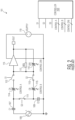
- FIG 3 is a circuit diagram of an AM radio receiver 300 that includes an amplifier circuit 301 according to one embodiment of the present invention.
- Amplifier circuit 301 receives an AM voltage signal from antenna 309 (represented in Figure 3 as a voltage source).
- antenna is a dipole antenna, but may be other types of antennas such as a loop antenna, whip antenna, or another type of antenna that is integrated into the design of an automobile.
- the output impedance of antenna 309 is 50 ohms, but may be of other impedances in other embodiments.
- receiver 300 is designed to receive and process AM signals in the frequency range of 535 to 1705 kilohertz, but may process signals in other frequency ranges in other embodiments.
- Circuit 301 includes an input capacitor 311 that receives the antenna signal at a first electrode, a switch 315 that includes a terminal electrically connected to the other electrode of input capacitor 311, and a divider capacitor 109 including one electrode electrically connected to ground and the other electrode electrically connected to a terminal of switch 315.
- a programmable capacitor bank 317 includes one terminal electrically connected to a terminal of switch 315 and to an electrode of capacitor 311. The other terminal of bank 317 is electrically connected to the input of amplifier 307.
- a programmable capacitor bank 319 includes one terminal electrically connected to the other terminal of switch 315 and to an electrode of divider capacitor 313. The other terminal of bank 319 is electrically connected to the input of amplifier 307.
- Circuit 301 includes a feedback resistor 323 and a feedback capacitor bank 321 that are each electrically connected between the input and output of amplifier 307.
- the high side power supply rail of amplifier 307 is powered from a voltage supply (VSUPPLY) and the low side power supply rail of amplifier 307 is connected to ground.
- amplifier 307 is differential amplifier where the inverting input of amplifier 307 is electrically connected to a terminal of bank 317 and to a terminal of bank 319, and the non inverting input is electrically connected to ground.
- Controller 305 provides switch control signal S3 for controlling the conductivity of switch 315 and provides multi signal line control signals CONTROL A, CONTROL B, and CONTROL CFB for controlling the capacitances of programmable capacitor banks 317, 319, and 321, respectively.
- controller 305 is implemented with a processor circuit (not shown), but in other embodiments, may be implemented with logic circuitry or with a combination thereof.
- Receiver 300 includes a wideband analog to digital converter (ADC) 341 that converts the modulated analog output of amplifier 307 to a digital signal.
- ADC wideband analog to digital converter
- the digital output of ADC 341 is then provided to circuitry 342 that filters the digital output, down converts the signal from the modulated frequency of the digital output, and demodulates the down converted signal to produce the transmitted information that can be played on a speaker (not shown).
- Other types of receivers may process the amplified signal in other ways and/or with other types of circuitry.
- Receiver 300 includes a rectifier 327 for providing a rectified DC voltage of the alternating current (AC) output of amplifier 307.
- the DC voltage is supplied to both a low voltage comparator 329 and a high voltage comparator 331.
- Low voltage comparator 329 compares the output of rectifier 327 with reference voltage VREFL and asserts the VCOMPL signal if the output is below reference voltage VREFL.
- High voltage comparator 331 compares the output of rectifier 327 with reference voltage VREFH and asserts the VCOMPH signal if the output of rectifier 327 is above reference voltage VREFH.
- Controller 305 uses the VCOMPH and VCOMPL signals to control the gain of amplifier 307 by adjusting the capacitance values of banks 317, 319, and 321 and to control switch 315 so as to keep the output of amplifier 307 in a voltage range as defined by voltage references VREFL and VREFH.
- controller 305 provides the amplifier gain status to circuitry 342 for processing the digital information.
- controller 305 may receive voltage information from ADC 341 for controlling the gain of amplifier 307.
- Controller 305 controls circuit 301 to operate in two different modes.
- switch 315 is open to where the input signal from antenna 309 passes through input capacitor 331 and through capacitor bank 317 to the input of amplifier 307.
- controller 305 adjusts the capacitance of bank 317 and the capacitance of bank 321 to adjust the gain of amplifier 307 to keep the voltage of the output of rectifier 327 between VREFL and VREFH.
- controller 305 When operating in the high gain mode, if the voltage of the output of rectifier 327 rises above VREFH, the capacitances of bank 317 and bank 321 are adjusted to decrease the gain to lower the output voltage of amplifier 307. If the antenna voltage keeps rising, controller 305 continues to lower the gain of amplifier 307 until it reaches a minimum gain.
- circuit 301 transitions to a low gain mode of operation where controller 305 closes switch 315 such that input capacitor 311 and divider capacitor 313 serve as a capacitor voltage divider to attenuate the signal being provided to the input of amplifier 307.
- controller 305 controls the capacitances of bank 317, bank 319, and bank 321 to adjust the gain of amplifier 307 to keep the output voltage of rectifier 327 between VREFL and VREFH.
- switch 315 may be implemented with a FET such as an NFET, switch 315 may exhibit a nonlinear on-resistance. This nonlinear on-resistance may generate voltage disturbances at each terminal of switch 315 where the voltage disturbances at the opposing terminals have opposite polarities.
- both programmable capacitor banks 317 and 319 are each controlled to provide a capacitance that is used to both control the gain of amplifier 307 but also to counteract the voltage disturbances on each terminal of switch 315.
- CA is the capacitance of bank 317
- CB is the capacitance of bank 319
- C1 is the capacitance of input capacitor 311
- C2 is the capacitance of divider capacitor 313.
- feasibly maintain the ratio of C 1 /C 2 means that the ratio C A /C B of the capacitances of the capacitor banks 317 and 319 are programmed to be as close to the ratio of C 1 /C 2 as possible given the configurations of the capacitor banks.
- the ratio of C A /C B may not exactly match C 1 /C 2 .
- the weighted sums of the voltages of banks 317 and 319 cancel out the disturbances at the switch terminals that are due to the nonlinearity of the on-resistance of the switch 315.
- antenna 309 is implemented in a car (e.g., embedded in a rear window).
- Capacitors 311 and 313 are discrete devices that are mounted on a circuit board 303 and are each of a fixed capacitance value.
- the remaining circuitry of receiver 300 shown in Figure 1 is implemented in an integrated circuit 302 mounted to the circuit board.
- a receiver may be implemented differently in other embodiments.
- capacitors 311 and 313 could be implemented in an integrated circuit with the remaining portion of amplifier circuit 301.
- the feedback capacitor e.g., bank 321
- switch 315 may be implemented with other types of switches such as a PFET or passgate.
- some of the functions of circuitry 342 may be implemented with analog circuitry.
- input capacitor 311 is 1 nF
- divider capacitor 313 is 12 nF
- feedback capacitor bank 321 is 10 pF.
- these capacitances may be of other values in other embodiments.
- the programmable capacitor banks 317, 319, and 321 are configured to adjust of the gain of amplifier 307 at 3 dB intervals. However, the gain of amplifier 307 may be adjusted at other intervals in other embodiments.
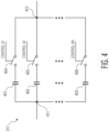
- FIG. 4 is a circuit diagram of programmable capacitor bank 317 according to one embodiment.
- bank 317 includes multiple capacitors with capacitors 401, 402, and 403 being shown.
- Each capacitor 401, 402, and 403 is selectively enabled by the closure of a corresponding switch 404, 405, and 406, respectively, as controlled by a signal CONTROL A1, CONTROL A2, and CONTROL AN, respectively, of multiline signal Control A provided by controller 305 (see Figure 3 ).
- switches 404-406 are implemented with NFETs, but may be implemented with other types of switches (e.g., PFETs, pass gates) in other embodiments.
- Bank terminal 411 is connected to a terminal of switch 315 and bank terminal 412 is connected to the input of amplifier 307.
- each capacitor 401-403 of bank 317 is the same size. In other embodiments, capacitors 401-403 are of different sizes. Although Figure 4 shows three capacitors, other embodiments may include more capacitors (e.g., 8, 10, 16 etc.).
- bank 317 is capable of provide a capacitance that ranges from 0 pf to 320 pf based on the assertion of different combinations of the CONTROL A signals. However, a capacitor bank may provide other capacitance values in other embodiments.
- FIG. 5 is a circuit diagram of programmable capacitor bank 319 according to one embodiment.
- bank 319 includes multiple capacitors with capacitors 501, 502, and 503 being shown.
- Each capacitor 501, 502, and 503 is selectively enabled by the closure of a corresponding switch 504, 505, and 506, respectively, as controlled by a signal CONTROL B1, CONTROL B2 and CONTROL BN, respectively, of multiline signal Control B provided by controller 305 (see Figure 3 ).
- switches 504-506 are implemented with NFETs, but may be implemented with other types of switches (e.g., PFETs, pass gates) in other embodiments.
- Bank terminal 511 is connected to a terminal of switch 315 and bank terminal 512 is connected to the input of amplifier 307.
- each capacitor 501-503 of a bank is the same size. In other embodiments, capacitors 501-503 are of different sizes. Although Figure 5 shows three capacitors, other embodiments may include more capacitors (e.g., 8, 10, 16 etc.).
- bank 319 is capable of provide a capacitance that ranges from 0 pf to 320 pf based on the assertion of different combinations of the CONTROL B signals. However, a capacitor bank may provide other capacitance values in other embodiments. When in the high gain mode of operation, all switches 504-506 are open such that there is no signal path from terminal 511 to terminal 512 through bank 319 and no capacitors of bank 319 are enabled.
- Figure 6 shows a state diagram of the operation of circuit 301 according to one embodiment.
- controller 305 adjusts the capacitance of bank 317 to control the gain of amplifier 307.
- controller 305 adjusts the capacitance of banks 317 and 319 to control the gain of amplifier 307.
- circuit 301 transitions from the high gain operating mode 601 to the low gain operating mode 603 when the voltage of antenna 309 rises above a threshold voltage level.
- the threshold voltage level corresponds to the output of rectifier 327 rising above VREFH when circuit 301 is set on the lowest amplifier gain in the high gain operating mode 601.
- circuit 301 transitions from the low gain operating mode 603 to the high gain operating mode 601 when the voltage of antenna 309 falls below a threshold voltage level.
- the threshold voltage level corresponds to the output of rectifier 327 falling below VREFL when circuit 301 is set on the highest amplifier gain of the low gain operating mode 603.
- circuit 301 may include a hysteresis feature where the threshold voltage in transitioning from mode 601 to mode 603 is higher than the threshold antenna voltage in transitioning from mode 603 to mode 601.
- providing an amplifier circuit that includes two programmable capacitor banks that are coupled to opposing terminals of a switch may provide for an amplifier circuit that can implement a capacitor voltage divider with a switch while minimizing the voltage distortion due to the switch. Accordingly, such an amplifier circuit can be utilized over a wider range of input voltages.
- amplifier circuit 301 is shown as receiving an antenna voltage from antenna 309 in Figure 3 , circuit 301 may be used to amply other signals from other devices in other embodiments.
- a circuit in one embodiment, includes an input node, an input capacitor including a first electrode electrically coupled to the input node, an amplifier, a first programmable capacitor bank including a first terminal electrically coupled to a second electrode of the input capacitor and a second terminal electrically coupled to an input of the amplifier, a switch including a first terminal couple to the second electrode of the input capacitor and to the first terminal of the first programmable capacitor bank, a second programmable capacitor bank including a first terminal electrically coupled to a second terminal of the switch and including a second terminal electrically coupled to the input of the amplifier, a divider capacitor including a first electrode electrically coupled to the second terminal of the switch and electrically coupled to the first terminal of the second programmable capacitor bank, and a controller including an output to control the conductivity of the switch.
- the switch is open such that there is no conductive path between its first terminal and its second terminal through the switch and the input capacitor and the divider capacitor are not configured as a capacitor voltage divider.
- the switch is closed such that there is a conductive path between its first terminal and its second terminal through the switch and the input capacitor and the divider capacitor are configured as a capacitor voltage divider.
- a capacitance provided by the first programmable capacitor bank but not a capacitance provided by the second programmable capacitor bank is adjusted to control the gain of the amplifier.
- the capacitance provided by the first programmable capacitor bank and the capacitance provided by the second programmable capacitor bank are each adjusted to control the gain of the amplifier.
- a method for amplifying a signal includes in a first mode of operation, providing an input signal from a first node, through an input capacitor, through a first programmable capacitor bank, and to an input of an amplifier.
- a switch is open such that there is no signal path from the input capacitor to a divider capacitor through the switch, and during the first mode of operation, a capacitance of the first programmable capacitor bank is adjusted to control a gain of the amplifier but a capacitance of a second programmable capacitor bank is not adjusted to control the gain of the amplifier.
- the input signal is provided from the first node through the input capacitor where the switch is closed to provide a signal path through the switch from an electrode of the input capacitor to the divider capacitor where the input capacitor and the divider capacitor are configured as a capacitor voltage divider such a signal at a node between the input capacitor and divider capacitor is provided through the first programmable capacitor bank and through the second programmable capacitor bank to the input of the amplifier.
- the capacitance of the first programmable capacitor bank and the capacitance of the second programmable capacitor bank are adjusted to control the gain of the amplifier.
- a circuit in another embodiment, includes a switch including a first terminal and a second terminal, an amplifier, and a first programmable capacitor bank including a first terminal electrically coupled to the first terminal of the switch and including a second terminal electrically coupled to an input of the amplifier.
- the circuit includes a second programmable capacitor bank including a first terminal electrically coupled to the second terminal of the switch and including a second terminal electrically coupled to the input of the amplifier.
- the circuit includes a controller including an output to control the conductivity of the switch.
- a capacitance provided by the first programmable capacitor bank but not a capacitance provided by the second programmable capacitor bank is adjusted to control a gain of the amplifier.
- the capacitance provided by the first programmable capacitor bank and the capacitance provided by the second programmable capacitor bank are each adjusted to control the gain of the amplifier.
Landscapes
- Engineering & Computer Science (AREA)
- Power Engineering (AREA)
- Physics & Mathematics (AREA)
- Nonlinear Science (AREA)
- Computer Hardware Design (AREA)
- Computing Systems (AREA)
- General Engineering & Computer Science (AREA)
- Mathematical Physics (AREA)
- Microelectronics & Electronic Packaging (AREA)
- Amplifiers (AREA)
- Control Of Amplification And Gain Control (AREA)
Abstract
An amplifier circuit that includes a capacitor voltage divider that is selectively enabled with a switch. The circuit includes two capacitor banks where the banks are electrically coupled to opposing side terminals of the switch. When the capacitor voltage divider is not enabled, one bank is adjusted to control the gain of the amplifier. When the capacitor voltage divider is enabled, both banks are used to control the gain of the amplifier.
Description
- This invention relates to distortion compensation for a switch in an amplifier circuit.
- Amplifiers are used to increase or adjust the amplitude of a signal for further processing. Some amplifier circuits include a selectively enabled capacitor voltage divider used in adjusting the gain of the amplifier.
- The present invention may be better understood, and its numerous objects, features, and advantages made apparent to those skilled in the art by referencing the accompanying drawings.
-
Figure 1 is a circuit diagram of a prior art amplifier circuit. -
Figure 2 is a circuit diagram of a prior art amplifier circuit. -
Figure 3 is a circuit diagram of an AM radio receiver with an amplifier circuit according to one embodiment of the present invention. -
Figure 4 is a circuit diagram of a programmable capacitor bank according to one embodiment of the present invention. -
Figure 5 is a circuit diagram of a programmable capacitor bank according to one embodiment of the present invention. -
Figure 6 is a state diagram showing the operation of an amplifier circuit according to one embodiment of the present invention. - The use of the same reference symbols in different drawings indicates identical items unless otherwise noted. The Figures are not necessarily drawn to scale.
- The following sets forth a detailed description of a mode for carrying out the invention. The description is intended to be illustrative of the invention and should not be taken to be limiting.
- Disclosed herein is an amplifier circuit that includes a capacitor voltage divider that is selectively enabled with a switch. The circuit includes two capacitor banks where the banks are electrically coupled to opposing side terminals of the switch. When the capacitor voltage divider is not enabled, one bank is adjusted to control the gain of the amplifier. When the capacitor voltage divider is enabled, both banks are used to control the gain of the amplifier.
- In some embodiments, utilizing programmable capacitor banks coupled to opposing switch terminals of a switch for controlling the gain of an amplifier may provide for an amplifier circuit where voltage distortions due to nonlinearities of the switch at the opposing switch terminals can be compensated for to reduce the voltage distortions.
-
Figures 1 and2 are prior art circuit diagrams of anamplifier circuit 101 in an amplitude modulation (AM) radio receiver showing two different modes of operation.Amplifier circuit 101 receives an AM volage signal from antenna 105 (represented inFigures 1 and2 as a voltage source).Circuit 101 includes aninput capacitor 107, aswitch 111, and adivider capacitor 109. Aprogrammable capacitor bank 114 is connected to one terminal ofswitch 111 and aprogrammable capacitor bank 115 is connected to the other terminal ofswitch 111.Switches bank 114 andbank 115, respectively, by providing a signal path to the input ofamplifier 116.Circuit 101 includes afeedback resistor 117 and afeedback capacitor bank 118 that are each connected to the input and output ofamplifier 116. The high side power supply rail ofamplifier 116 is powered from a voltage supply (VSUPPLY 119) and the low side power supply rail is electrically connected to ground.Circuit 101 includes acontroller 103 for providing the switch control signals S1, S2, and S3 for controllingswitches programmable capacitor banks -
Figure 1 showscircuit 101 whenswitch 112 is closed and switch 111 and 113 is open such that the input signal is provided through capacitor 102 and thoughprogrammable capacitor bank 114 to amplifier 116. During this mode of operation, the capacitances ofbanks amplifier 116 is within a desired voltage range for further processing. -
Figure 2 showscircuit 101 withswitch 112 open andswitches capacitors amplifier circuit 101. In this mode of operation, the capacitances ofbank 115 andbank 118 are controlled to control the gain ofamplifier 116 within a specified voltage range. -
Circuit 101 is placed in the configuration ofFigure 1 orFigure 2 , based on the voltage level of the output of amplifier 116 (VOUT) so as to keep the volage of VOUT within a specified range. If receiving a weak input signal fromantenna 105, the capacitor voltage divider is turned off because utilizing it may increase the equivalent input noise.
Becauseswitch 111 is typically implemented with an N type FET,switch 111 has a nonlinear on-resistance when closed. This nonlinearity produces distortion products by creating unwanted components at linear combinations of the fundamental frequencies. A distortion voltage distributes overcapacitors Figure 2 , a distortion voltage can appear at both opposing terminals ofswitch 111, where the distortion appearing at one terminal has the opposite polarity of the distortion at the other terminal and where the magnitude of the distortion is dependent upon the capacitances ofcapacitors -
Figure 3 is a circuit diagram of anAM radio receiver 300 that includes anamplifier circuit 301 according to one embodiment of the present invention.Amplifier circuit 301 receives an AM voltage signal from antenna 309 (represented inFigure 3 as a voltage source). In one embodiment, antenna is a dipole antenna, but may be other types of antennas such as a loop antenna, whip antenna, or another type of antenna that is integrated into the design of an automobile. In one embodiment, the output impedance ofantenna 309 is 50 ohms, but may be of other impedances in other embodiments. In one embodiment,receiver 300 is designed to receive and process AM signals in the frequency range of 535 to 1705 kilohertz, but may process signals in other frequency ranges in other embodiments. -
Circuit 301 includes aninput capacitor 311 that receives the antenna signal at a first electrode, aswitch 315 that includes a terminal electrically connected to the other electrode ofinput capacitor 311, and adivider capacitor 109 including one electrode electrically connected to ground and the other electrode electrically connected to a terminal ofswitch 315. Aprogrammable capacitor bank 317 includes one terminal electrically connected to a terminal ofswitch 315 and to an electrode ofcapacitor 311. The other terminal ofbank 317 is electrically connected to the input ofamplifier 307. Aprogrammable capacitor bank 319 includes one terminal electrically connected to the other terminal ofswitch 315 and to an electrode ofdivider capacitor 313. The other terminal ofbank 319 is electrically connected to the input ofamplifier 307.Circuit 301 includes afeedback resistor 323 and afeedback capacitor bank 321 that are each electrically connected between the input and output ofamplifier 307. The high side power supply rail ofamplifier 307 is powered from a voltage supply (VSUPPLY) and the low side power supply rail ofamplifier 307 is connected to ground. In one embodiment,amplifier 307 is differential amplifier where the inverting input ofamplifier 307 is electrically connected to a terminal ofbank 317 and to a terminal ofbank 319, and the non inverting input is electrically connected to ground.Controller 305 provides switch control signal S3 for controlling the conductivity ofswitch 315 and provides multi signal line control signals CONTROL A, CONTROL B, and CONTROL CFB for controlling the capacitances ofprogrammable capacitor banks controller 305 is implemented with a processor circuit (not shown), but in other embodiments, may be implemented with logic circuitry or with a combination thereof. -
Receiver 300 includes a wideband analog to digital converter (ADC) 341 that converts the modulated analog output ofamplifier 307 to a digital signal. The digital output ofADC 341 is then provided tocircuitry 342 that filters the digital output, down converts the signal from the modulated frequency of the digital output, and demodulates the down converted signal to produce the transmitted information that can be played on a speaker (not shown). Other types of receivers may process the amplified signal in other ways and/or with other types of circuitry. -
Receiver 300 includes arectifier 327 for providing a rectified DC voltage of the alternating current (AC) output ofamplifier 307. The DC voltage is supplied to both alow voltage comparator 329 and ahigh voltage comparator 331.Low voltage comparator 329 compares the output ofrectifier 327 with reference voltage VREFL and asserts the VCOMPL signal if the output is below reference voltage VREFL.High voltage comparator 331 compares the output ofrectifier 327 with reference voltage VREFH and asserts the VCOMPH signal if the output ofrectifier 327 is above reference voltage VREFH. -
Controller 305 uses the VCOMPH and VCOMPL signals to control the gain ofamplifier 307 by adjusting the capacitance values ofbanks switch 315 so as to keep the output ofamplifier 307 in a voltage range as defined by voltage references VREFL and VREFH. In some embodiments,controller 305 provides the amplifier gain status tocircuitry 342 for processing the digital information. In other embodiments,controller 305 may receive voltage information fromADC 341 for controlling the gain ofamplifier 307. -
Controller 305 controlscircuit 301 to operate in two different modes. In a high gain mode,switch 315 is open to where the input signal fromantenna 309 passes throughinput capacitor 331 and throughcapacitor bank 317 to the input ofamplifier 307. In the high gain mode,controller 305 adjusts the capacitance ofbank 317 and the capacitance ofbank 321 to adjust the gain ofamplifier 307 to keep the voltage of the output ofrectifier 327 between VREFL and VREFH. In one embodiment, the gain of amplifier 307 (H) in the high gain mode is given by:
bank 321, CA is the capacitance ofbank 317, and C1 is the capacitance ofinput capacitor 311. - When operating in the high gain mode, if the voltage of the output of
rectifier 327 rises above VREFH, the capacitances ofbank 317 andbank 321 are adjusted to decrease the gain to lower the output voltage ofamplifier 307. If the antenna voltage keeps rising,controller 305 continues to lower the gain ofamplifier 307 until it reaches a minimum gain. - If the antenna voltage continues to rise while at the minimum gain in the high gain mode,
circuit 301 transitions to a low gain mode of operation wherecontroller 305 closes switch 315 such thatinput capacitor 311 anddivider capacitor 313 serve as a capacitor voltage divider to attenuate the signal being provided to the input ofamplifier 307. In the low gain mode of operation,controller 305 controls the capacitances ofbank 317,bank 319, andbank 321 to adjust the gain ofamplifier 307 to keep the output voltage ofrectifier 327 between VREFL and VREFH. - Because
switch 315 may be implemented with a FET such as an NFET, switch 315 may exhibit a nonlinear on-resistance. This nonlinear on-resistance may generate voltage disturbances at each terminal ofswitch 315 where the voltage disturbances at the opposing terminals have opposite polarities. - Accordingly, in the low gain mode of operation, both
programmable capacitor banks amplifier 307 but also to counteract the voltage disturbances on each terminal ofswitch 315. - In one embodiment, to counteract the disturbances of each at each terminal of
switch 315, the capacitance ofbank 317 and the capacitance ofbank 319 are selected so as to feasibly maintain the ratio of:
bank 317, CB is the capacitance ofbank 319, C1 is the capacitance ofinput capacitor 311 and C2 is the capacitance ofdivider capacitor 313. As used herein, feasibly maintain the ratio of C1/C2 means that the ratio CA/CB of the capacitances of thecapacitor banks capacitor banks banks switch 315. - In order to adjust the gain of
amplifier 307 in the low gain mode of operation, the total gain of CA + CB is adjusted with respect to the capacitance offeedback bank 321 wherein the gain of amplifier 307 (H) is given by:
- In one embodiment,
antenna 309 is implemented in a car (e.g., embedded in a rear window).Capacitors circuit board 303 and are each of a fixed capacitance value. The remaining circuitry ofreceiver 300 shown inFigure 1 is implemented in anintegrated circuit 302 mounted to the circuit board. However, a receiver may be implemented differently in other embodiments. For example,capacitors amplifier circuit 301. Also in other embodiments, the feedback capacitor (e.g., bank 321) could be implemented with a fixed capacitor. Also in other embodiments, switch 315 may be implemented with other types of switches such as a PFET or passgate. Furthermore, some of the functions ofcircuitry 342 may be implemented with analog circuitry. - In one embodiment,
input capacitor 311 is 1 nF,divider capacitor 313 is 12 nF, andfeedback capacitor bank 321 is 10 pF. However, these capacitances may be of other values in other embodiments. In one embodiment, theprogrammable capacitor banks amplifier 307 at 3 dB intervals. However, the gain ofamplifier 307 may be adjusted at other intervals in other embodiments. -
Figure 4 is a circuit diagram ofprogrammable capacitor bank 317 according to one embodiment. In the embodiment ofFigure 4 ,bank 317 includes multiple capacitors withcapacitors capacitor corresponding switch Figure 3 ). In one embodiment, switches 404-406 are implemented with NFETs, but may be implemented with other types of switches (e.g., PFETs, pass gates) in other embodiments.Bank terminal 411 is connected to a terminal ofswitch 315 andbank terminal 412 is connected to the input ofamplifier 307. In one embodiment, each capacitor 401-403 ofbank 317 is the same size. In other embodiments, capacitors 401-403 are of different sizes. AlthoughFigure 4 shows three capacitors, other embodiments may include more capacitors (e.g., 8, 10, 16 etc.). In one embodiment,bank 317 is capable of provide a capacitance that ranges from 0 pf to 320 pf based on the assertion of different combinations of the CONTROL A signals. However, a capacitor bank may provide other capacitance values in other embodiments. -
Figure 5 is a circuit diagram ofprogrammable capacitor bank 319 according to one embodiment. In the embodiment ofFigure 5 ,bank 319 includes multiple capacitors withcapacitors capacitor corresponding switch Figure 3 ). In one embodiment, switches 504-506 are implemented with NFETs, but may be implemented with other types of switches (e.g., PFETs, pass gates) in other embodiments.Bank terminal 511 is connected to a terminal ofswitch 315 andbank terminal 512 is connected to the input ofamplifier 307. In one embodiment, each capacitor 501-503 of a bank is the same size. In other embodiments, capacitors 501-503 are of different sizes. AlthoughFigure 5 shows three capacitors, other embodiments may include more capacitors (e.g., 8, 10, 16 etc.). In one embodiment,bank 319 is capable of provide a capacitance that ranges from 0 pf to 320 pf based on the assertion of different combinations of the CONTROL B signals. However, a capacitor bank may provide other capacitance values in other embodiments. When in the high gain mode of operation, all switches 504-506 are open such that there is no signal path from terminal 511 to terminal 512 throughbank 319 and no capacitors ofbank 319 are enabled. -
Figure 6 shows a state diagram of the operation ofcircuit 301 according to one embodiment. When operating in a high gain mode (601),controller 305 adjusts the capacitance ofbank 317 to control the gain ofamplifier 307. When operating in thelow gain mode 603,controller 305 adjusts the capacitance ofbanks amplifier 307. - In one embodiment,
circuit 301 transitions from the highgain operating mode 601 to the lowgain operating mode 603 when the voltage ofantenna 309 rises above a threshold voltage level. In one embodiment, the threshold voltage level corresponds to the output ofrectifier 327 rising above VREFH whencircuit 301 is set on the lowest amplifier gain in the highgain operating mode 601. - In another embodiment,
circuit 301 transitions from the lowgain operating mode 603 to the highgain operating mode 601 when the voltage ofantenna 309 falls below a threshold voltage level. In one embodiment, the threshold voltage level corresponds to the output ofrectifier 327 falling below VREFL whencircuit 301 is set on the highest amplifier gain of the lowgain operating mode 603. In some embodiments,circuit 301 may include a hysteresis feature where the threshold voltage in transitioning frommode 601 tomode 603 is higher than the threshold antenna voltage in transitioning frommode 603 tomode 601. - In one embodiment, providing an amplifier circuit that includes two programmable capacitor banks that are coupled to opposing terminals of a switch may provide for an amplifier circuit that can implement a capacitor voltage divider with a switch while minimizing the voltage distortion due to the switch. Accordingly, such an amplifier circuit can be utilized over a wider range of input voltages.
- Although
amplifier circuit 301 is shown as receiving an antenna voltage fromantenna 309 inFigure 3 ,circuit 301 may be used to amply other signals from other devices in other embodiments. - Features shown or described with respect to one embodiment described herein may implemented with other embodiments described herein.
- In one embodiment, a circuit includes an input node, an input capacitor including a first electrode electrically coupled to the input node, an amplifier, a first programmable capacitor bank including a first terminal electrically coupled to a second electrode of the input capacitor and a second terminal electrically coupled to an input of the amplifier, a switch including a first terminal couple to the second electrode of the input capacitor and to the first terminal of the first programmable capacitor bank, a second programmable capacitor bank including a first terminal electrically coupled to a second terminal of the switch and including a second terminal electrically coupled to the input of the amplifier, a divider capacitor including a first electrode electrically coupled to the second terminal of the switch and electrically coupled to the first terminal of the second programmable capacitor bank, and a controller including an output to control the conductivity of the switch. During a first mode of operation, the switch is open such that there is no conductive path between its first terminal and its second terminal through the switch and the input capacitor and the divider capacitor are not configured as a capacitor voltage divider. During the second mode of operation, the switch is closed such that there is a conductive path between its first terminal and its second terminal through the switch and the input capacitor and the divider capacitor are configured as a capacitor voltage divider. During the first mode of operation, a capacitance provided by the first programmable capacitor bank but not a capacitance provided by the second programmable capacitor bank is adjusted to control the gain of the amplifier. During the second mode of operation, the capacitance provided by the first programmable capacitor bank and the capacitance provided by the second programmable capacitor bank are each adjusted to control the gain of the amplifier.
- In another embodiment, a method for amplifying a signal includes in a first mode of operation, providing an input signal from a first node, through an input capacitor, through a first programmable capacitor bank, and to an input of an amplifier. During the first mode of operation, a switch is open such that there is no signal path from the input capacitor to a divider capacitor through the switch, and during the first mode of operation, a capacitance of the first programmable capacitor bank is adjusted to control a gain of the amplifier but a capacitance of a second programmable capacitor bank is not adjusted to control the gain of the amplifier. In a second mode of operation, the input signal is provided from the first node through the input capacitor where the switch is closed to provide a signal path through the switch from an electrode of the input capacitor to the divider capacitor where the input capacitor and the divider capacitor are configured as a capacitor voltage divider such a signal at a node between the input capacitor and divider capacitor is provided through the first programmable capacitor bank and through the second programmable capacitor bank to the input of the amplifier. During the first mode of operation, the capacitance of the first programmable capacitor bank and the capacitance of the second programmable capacitor bank are adjusted to control the gain of the amplifier.
- In another embodiment, a circuit includes a switch including a first terminal and a second terminal, an amplifier, and a first programmable capacitor bank including a first terminal electrically coupled to the first terminal of the switch and including a second terminal electrically coupled to an input of the amplifier. The circuit includes a second programmable capacitor bank including a first terminal electrically coupled to the second terminal of the switch and including a second terminal electrically coupled to the input of the amplifier. The circuit includes a controller including an output to control the conductivity of the switch. During a first mode of operation, the switch is open such that there is no conductive path between its first terminal and its second terminal through the switch. During a second mode of operation, the switch is closed such that there is a conductive path between its first terminal and its second terminal through the switch. During the first mode of operation, a capacitance provided by the first programmable capacitor bank but not a capacitance provided by the second programmable capacitor bank is adjusted to control a gain of the amplifier. During the second mode of operation, the capacitance provided by the first programmable capacitor bank and the capacitance provided by the second programmable capacitor bank are each adjusted to control the gain of the amplifier.
- While particular embodiments of the present invention have been shown and described, it will be recognized to those skilled in the art that, based upon the teachings herein, further changes and modifications may be made without departing from this invention and its broader aspects, and thus, the appended claims are to encompass within their scope all such changes and modifications as are within the scope of this invention.
Claims (15)
- A circuit comprising:an input node;an input capacitor including a first electrode electrically coupled to the input node;an amplifier;a first programmable capacitor bank including a first terminal electrically coupled to a second electrode of the input capacitor and a second terminal electrically coupled to an input of the amplifier;a switch including a first terminal couple to the second electrode of the input capacitor and to the first terminal of the first programmable capacitor bank;a second programmable capacitor bank including a first terminal electrically coupled to a second terminal of the switch and including a second terminal electrically coupled to the input of the amplifier;a divider capacitor including a first electrode electrically coupled to the second terminal of the switch and electrically coupled to the first terminal of the second programmable capacitor bank;a controller including an output to control the conductivity of the switch, wherein during a first mode of operation, the switch is open such that there is no conductive path between its first terminal and its second terminal through the switch and the input capacitor and the divider capacitor are not configured as a capacitor voltage divider, wherein during the second mode of operation, the switch is closed such that there is a conductive path between its first terminal and its second terminal through the switch and the input capacitor and the divider capacitor are configured as a capacitor voltage divider;wherein during the first mode of operation, a capacitance provided by the first programmable capacitor bank but not a capacitance provided by the second programmable capacitor bank is adjusted to control a gain of the amplifier, wherein during the second mode of operation, the capacitance provided by the first programmable capacitor bank and the capacitance provided by the second programmable capacitor bank are each adjusted to control the gain of the amplifier.
- The circuit of claim 1 wherein during the first mode of operation, the capacitance provided by the first programmable capacitor bank but not the capacitance provided by the second programmable capacitor bank is adjusted to control the gain of the amplifier in response to a change in an output voltage of the amplifier, wherein during the second mode of operation, the capacitance provided by the first programmable capacitor bank and the capacitance provided by the second programmable capacitor bank are each adjusted to control the gain of the amplifier in response to a change in an output voltage of the amplifier.
- The circuit of claim 1 or 2 wherein the second programmable capacitor bank includes a plurality of switchable capacitors and a plurality of switches each for selectively enabling a capacitor of the plurality of switchable capacitors, wherein during the first mode of operation, all switches of the plurality of switches are open such that no capacitor of the plurality of switchable capacitors is enabled.
- The circuit of any preceding claim wherein during the second mode of operation, the capacitance of the first programmable capacitor bank and the capacitance of the second programmable capacitor bank are adjusted to adjust a total capacitance of the capacitance of the first programmable capacitor bank and the capacitance of the second programmable capacitor bank to control the gain of the amplifier and to feasibly maintain the ratio of the capacitance of the first programmable capacitor bank to the capacitance of the second programmable capacitor bank.
- The circuit of any preceding claim wherein during the second mode of operation, the capacitance of the first programmable capacitor bank and the capacitance of the second programmable capacitor bank are selected such that the ratio of the capacitance of the first programmable capacitor bank to the capacitance of the second programmable capacitor bank is feasibly maintained to the ratio of a capacitance of the input capacitor to a capacitance of the divider capacitor.
- The circuit of any preceding claim further comprising:
an antenna, the input node is electrically coupled to the antenna to receive a voltage of the antenna during the first mode of operation and during the second mode of operation. - The circuit of claim 6 wherein the antenna is configured to receive an amplitude modulated, AM, radio signal.
- The circuit of any preceding claim further comprising:a programmable feedback capacitor bank having a first terminal electrically coupled to the input of the amplifier and a second terminal electrically coupled to the output of the amplifier;wherein during the first mode of operation and during the second mode of operation, a capacitance provided by the programmable feedback capacitor bank is adjusted to control the gain of the amplifier.
- The circuit of any preceding claim 1 wherein the input is signal is characterized as an alternating current, AC, signal.
- A method for amplifying a signal comprising:in a first mode of operation, providing an input signal from a first node, through an input capacitor, through a first programmable capacitor bank, and to an input of an amplifier, wherein during the first mode of operation, a switch is open such that there is no signal path from the input capacitor to a divider capacitor through the switch, wherein during the first mode of operation, a capacitance of the first programmable capacitor bank is adjusted to control a gain of the amplifier but a capacitance of a second programmable capacitor bank is not adjusted to control the gain of the amplifier;in a second mode of operation, the input signal is provided from the first node through the input capacitor where the switch is closed to provide a signal path through the switch from an electrode of the input capacitor to the divider capacitor where the input capacitor and the divider capacitor are configured as a capacitor voltage divider such a signal at a node between the input capacitor and divider capacitor is provided through the first programmable capacitor bank and through the second programmable capacitor bank to the input of the amplifier, wherein during the second mode of operation, the capacitance of the first programmable capacitor bank and the capacitance of the second programmable capacitor bank are adjusted to control the gain of the amplifier.
- The method of claim 10 wherein during the first mode of operation, the capacitance provided by the first programmable capacitor bank but not the capacitance provided by the second programmable capacitor bank is adjusted to control the gain of the amplifier in response to a change in an output voltage of the amplifier, wherein during the second mode of operation, the capacitance provided by the first programmable capacitor bank and the capacitance provided by the second programmable capacitor bank are each adjusted to control the gain of the amplifier in response to a change in an output voltage of the amplifier.
- The method of claim 10 or 11 wherein during the second mode of operation, the capacitance of the first programmable capacitor bank and the capacitance of the second programmable capacitor bank are adjusted to adjust a total capacitance of the capacitance of the first programmable capacitor bank and the capacitance of the second programmable capacitor bank to control the gain of the amplifier and to feasibly maintain the ratio of the capacitance of the first programmable capacitor bank to the capacitance of the second programmable capacitor bank.
- The method of any of claims 10 to 12 wherein during the second mode of operation, the capacitance of the first programmable capacitor bank and the capacitance of the second programmable capacitor bank are selected such that the ratio of the capacitance of the first programmable capacitor bank to the capacitance of the second programmable capacitor bank is feasibly maintained to the ratio of a capacitance of the input capacitor to a capacitance of the divider capacitor.
- The method of any of claims 10 to 13 wherein the input signal is produced by an antenna.
- The method of any of claims 10 to 14 wherein during the first mode of operation and during the second mode of operation, a capacitance provided by a feedback programmable capacitor bank is adjusted to control the gain of the amplifier, the feedback programmable capacitor bank including a first terminal electrically coupled to the input of the amplifier and a second terminal electrically coupled to an output of the amplifier.
Applications Claiming Priority (1)
| Application Number | Priority Date | Filing Date | Title |
|---|---|---|---|
| US18/325,555 US12597889B2 (en) | 2023-05-30 | 2023-05-30 | Distortion compensation for a switch in an amplifier circuit |
Publications (1)
| Publication Number | Publication Date |
|---|---|
| EP4472071A1 true EP4472071A1 (en) | 2024-12-04 |
Family
ID=91128139
Family Applications (1)
| Application Number | Title | Priority Date | Filing Date |
|---|---|---|---|
| EP24175927.3A Pending EP4472071A1 (en) | 2023-05-30 | 2024-05-15 | Distortion compensation for a switch in an amplifier circuit |
Country Status (3)
| Country | Link |
|---|---|
| US (1) | US12597889B2 (en) |
| EP (1) | EP4472071A1 (en) |
| CN (1) | CN119070757A (en) |
Citations (1)
| Publication number | Priority date | Publication date | Assignee | Title |
|---|---|---|---|---|
| CN103378813A (en) * | 2012-04-16 | 2013-10-30 | 英飞凌科技股份有限公司 | Systems and methods for high input capacitance signal amplifiers |
Family Cites Families (4)
| Publication number | Priority date | Publication date | Assignee | Title |
|---|---|---|---|---|
| JP6473931B2 (en) | 2014-05-29 | 2019-02-27 | パナソニックIpマネジメント株式会社 | Resin substrate with support substrate, manufacturing method thereof, and electronic device using the resin substrate |
| US9941849B1 (en) * | 2017-02-10 | 2018-04-10 | Psemi Corporation | Programmable optimized band switching LNA for operation in multiple narrow-band frequency ranges |
| US10381991B1 (en) * | 2018-02-02 | 2019-08-13 | Psemi Corporation | Drain sharing split LNA |
| TWI783808B (en) * | 2021-12-02 | 2022-11-11 | 瑞昱半導體股份有限公司 | Signal receiving apparatus and programmable gain amplifier having mode-switching mechanism |
-
2023
- 2023-05-30 US US18/325,555 patent/US12597889B2/en active Active
-
2024
- 2024-05-15 EP EP24175927.3A patent/EP4472071A1/en active Pending
- 2024-05-28 CN CN202410674776.5A patent/CN119070757A/en active Pending
Patent Citations (1)
| Publication number | Priority date | Publication date | Assignee | Title |
|---|---|---|---|---|
| CN103378813A (en) * | 2012-04-16 | 2013-10-30 | 英飞凌科技股份有限公司 | Systems and methods for high input capacitance signal amplifiers |
Non-Patent Citations (1)
| Title |
|---|
| KHATAVKAR PRATHAMESH ET AL: "432 nW per Channel 130 nV/rtHz ECG Acquisition Front End With Multifrequency Chopping", IEEE TRANSACTIONS ON VERY LARGE SCALE INTEGRATION (VLSI) SYSTEMS, IEEE SERVICE CENTER, PISCATAWAY, NJ, USA, vol. 27, no. 9, 1 September 2019 (2019-09-01), pages 2021 - 2032, XP011742472, ISSN: 1063-8210, [retrieved on 20190822], DOI: 10.1109/TVLSI.2019.2910202 * |
Also Published As
| Publication number | Publication date |
|---|---|
| US20240405728A1 (en) | 2024-12-05 |
| US12597889B2 (en) | 2026-04-07 |
| CN119070757A (en) | 2024-12-03 |
Similar Documents
| Publication | Publication Date | Title |
|---|---|---|
| US10243531B1 (en) | Apparatus and method for centrally controlling common mode voltages for a set of receivers | |
| US9647618B1 (en) | System and method for controlling common mode voltage via replica circuit and feedback control | |
| US10797916B2 (en) | EHF receiver architecture with dynamically adjustable discrimination threshold | |
| US6801068B2 (en) | Delay clock pulse-width adjusting circuit for intermediate frequency or high frequency | |
| US10461701B2 (en) | System and method for reducing output harmonics | |
| US20080018393A1 (en) | Offset voltage correction circuit and class D amplifier | |
| JPS62274906A (en) | High frequency amplifier | |
| US11658628B2 (en) | Semiconductor integrated circuit, receiving device, and DC offset cancellation method | |
| EP3197048B1 (en) | Power amplifier system and associated control circuit and control method | |
| US12244280B2 (en) | Signal processing circuit | |
| CN118232852A (en) | Calibration device and calibration method | |
| US7636547B2 (en) | Reactance adjuster, transceiver and transmitter using the reactance adjuster, signal processing circuit suitable for use in the reactance adjuster, the transceiver, and the transmitter, reactance adjusting method, transmitting method, and receiving method | |
| US5438694A (en) | Distortion compensation for a pulsewidth-modulated circuit | |
| US11683015B2 (en) | Class-D amplifier with deadtime distortion compensation | |
| US12597889B2 (en) | Distortion compensation for a switch in an amplifier circuit | |
| US11012040B2 (en) | Radio frequency amplifier having adaptive power supply capability | |
| US8581563B2 (en) | Power supply device | |
| US20060202756A1 (en) | Radio-frequency power amplifier apparatus and method of adjusting output power thereof | |
| CN104836548A (en) | Input circuit compensating duty ratio distortion of input signal | |
| US9960947B2 (en) | Compensation circuit of power amplifier and associated compensation method | |
| EP0418899B1 (en) | Amplifier circuit | |
| EP3952107A1 (en) | Amplifier circuit using voltage-to-current conversion to achieve unity feedback factor and input common-mode rejection for linear amplifier and associated envelope tracking supply modulator using the same | |
| US8213882B2 (en) | Voltage converting circuit and radio communication apparatus | |
| KR102652748B1 (en) | Differential envelope detector with common mode feedback | |
| US11218232B1 (en) | DC offset calibration system and method |
Legal Events
| Date | Code | Title | Description |
|---|---|---|---|
| PUAI | Public reference made under article 153(3) epc to a published international application that has entered the european phase |
Free format text: ORIGINAL CODE: 0009012 |
|
| STAA | Information on the status of an ep patent application or granted ep patent |
Free format text: STATUS: THE APPLICATION HAS BEEN PUBLISHED |
|
| AK | Designated contracting states |
Kind code of ref document: A1 Designated state(s): AL AT BE BG CH CY CZ DE DK EE ES FI FR GB GR HR HU IE IS IT LI LT LU LV MC ME MK MT NL NO PL PT RO RS SE SI SK SM TR |
|
| STAA | Information on the status of an ep patent application or granted ep patent |
Free format text: STATUS: REQUEST FOR EXAMINATION WAS MADE |
|
| 17P | Request for examination filed |
Effective date: 20250604 |