EP4472050A1 - Commutation assistance by controlling the shape of the current wave in a bidirectional totem pole converter - Google Patents
Commutation assistance by controlling the shape of the current wave in a bidirectional totem pole converter Download PDFInfo
- Publication number
- EP4472050A1 EP4472050A1 EP24315250.1A EP24315250A EP4472050A1 EP 4472050 A1 EP4472050 A1 EP 4472050A1 EP 24315250 A EP24315250 A EP 24315250A EP 4472050 A1 EP4472050 A1 EP 4472050A1
- Authority
- EP
- European Patent Office
- Prior art keywords
- current
- voltage
- waveform
- digital
- node
- Prior art date
- Legal status (The legal status is an assumption and is not a legal conclusion. Google has not performed a legal analysis and makes no representation as to the accuracy of the status listed.)
- Pending
Links
Images



Classifications
-
- H—ELECTRICITY
- H02—GENERATION; CONVERSION OR DISTRIBUTION OF ELECTRIC POWER
- H02M—APPARATUS FOR CONVERSION BETWEEN AC AND AC, BETWEEN AC AND DC, OR BETWEEN DC AND DC, AND FOR USE WITH MAINS OR SIMILAR POWER SUPPLY SYSTEMS; CONVERSION OF DC OR AC INPUT POWER INTO SURGE OUTPUT POWER; CONTROL OR REGULATION THEREOF
- H02M1/00—Details of apparatus for conversion
- H02M1/42—Circuits or arrangements for compensating for or adjusting power factor in converters or inverters
- H02M1/4208—Arrangements for improving power factor of AC input
- H02M1/4233—Arrangements for improving power factor of AC input using a bridge converter comprising active switches
-
- H—ELECTRICITY
- H02—GENERATION; CONVERSION OR DISTRIBUTION OF ELECTRIC POWER
- H02M—APPARATUS FOR CONVERSION BETWEEN AC AND AC, BETWEEN AC AND DC, OR BETWEEN DC AND DC, AND FOR USE WITH MAINS OR SIMILAR POWER SUPPLY SYSTEMS; CONVERSION OF DC OR AC INPUT POWER INTO SURGE OUTPUT POWER; CONTROL OR REGULATION THEREOF
- H02M1/00—Details of apparatus for conversion
- H02M1/0048—Circuits or arrangements for reducing losses
- H02M1/0054—Transistor switching losses
-
- H—ELECTRICITY
- H02—GENERATION; CONVERSION OR DISTRIBUTION OF ELECTRIC POWER
- H02M—APPARATUS FOR CONVERSION BETWEEN AC AND AC, BETWEEN AC AND DC, OR BETWEEN DC AND DC, AND FOR USE WITH MAINS OR SIMILAR POWER SUPPLY SYSTEMS; CONVERSION OF DC OR AC INPUT POWER INTO SURGE OUTPUT POWER; CONTROL OR REGULATION THEREOF
- H02M1/00—Details of apparatus for conversion
- H02M1/0083—Converters characterised by their input or output configuration
- H02M1/0085—Partially controlled bridges
-
- H—ELECTRICITY
- H02—GENERATION; CONVERSION OR DISTRIBUTION OF ELECTRIC POWER
- H02M—APPARATUS FOR CONVERSION BETWEEN AC AND AC, BETWEEN AC AND DC, OR BETWEEN DC AND DC, AND FOR USE WITH MAINS OR SIMILAR POWER SUPPLY SYSTEMS; CONVERSION OF DC OR AC INPUT POWER INTO SURGE OUTPUT POWER; CONTROL OR REGULATION THEREOF
- H02M1/00—Details of apparatus for conversion
- H02M1/08—Circuits specially adapted for the generation of control voltages for semiconductor devices incorporated in static converters
- H02M1/081—Circuits specially adapted for the generation of control voltages for semiconductor devices incorporated in static converters wherein the phase of the control voltage is adjustable with reference to the AC source
-
- H—ELECTRICITY
- H02—GENERATION; CONVERSION OR DISTRIBUTION OF ELECTRIC POWER
- H02M—APPARATUS FOR CONVERSION BETWEEN AC AND AC, BETWEEN AC AND DC, OR BETWEEN DC AND DC, AND FOR USE WITH MAINS OR SIMILAR POWER SUPPLY SYSTEMS; CONVERSION OF DC OR AC INPUT POWER INTO SURGE OUTPUT POWER; CONTROL OR REGULATION THEREOF
- H02M1/00—Details of apparatus for conversion
- H02M1/08—Circuits specially adapted for the generation of control voltages for semiconductor devices incorporated in static converters
- H02M1/088—Circuits specially adapted for the generation of control voltages for semiconductor devices incorporated in static converters for the simultaneous control of series or parallel connected semiconductor devices
-
- H—ELECTRICITY
- H02—GENERATION; CONVERSION OR DISTRIBUTION OF ELECTRIC POWER
- H02M—APPARATUS FOR CONVERSION BETWEEN AC AND AC, BETWEEN AC AND DC, OR BETWEEN DC AND DC, AND FOR USE WITH MAINS OR SIMILAR POWER SUPPLY SYSTEMS; CONVERSION OF DC OR AC INPUT POWER INTO SURGE OUTPUT POWER; CONTROL OR REGULATION THEREOF
- H02M7/00—Conversion of AC power input into DC power output; Conversion of DC power input into AC power output
- H02M7/02—Conversion of AC power input into DC power output without possibility of reversal
- H02M7/04—Conversion of AC power input into DC power output without possibility of reversal by static converters
- H02M7/12—Conversion of AC power input into DC power output without possibility of reversal by static converters using discharge tubes with control electrode or semiconductor devices with control electrode
- H02M7/145—Conversion of AC power input into DC power output without possibility of reversal by static converters using discharge tubes with control electrode or semiconductor devices with control electrode using devices of a thyratron or thyristor type requiring extinguishing means
- H02M7/155—Conversion of AC power input into DC power output without possibility of reversal by static converters using discharge tubes with control electrode or semiconductor devices with control electrode using devices of a thyratron or thyristor type requiring extinguishing means using semiconductor devices only
- H02M7/162—Conversion of AC power input into DC power output without possibility of reversal by static converters using discharge tubes with control electrode or semiconductor devices with control electrode using devices of a thyratron or thyristor type requiring extinguishing means using semiconductor devices only in a bridge configuration
- H02M7/1623—Conversion of AC power input into DC power output without possibility of reversal by static converters using discharge tubes with control electrode or semiconductor devices with control electrode using devices of a thyratron or thyristor type requiring extinguishing means using semiconductor devices only in a bridge configuration with control circuit
-
- H—ELECTRICITY
- H02—GENERATION; CONVERSION OR DISTRIBUTION OF ELECTRIC POWER
- H02M—APPARATUS FOR CONVERSION BETWEEN AC AND AC, BETWEEN AC AND DC, OR BETWEEN DC AND DC, AND FOR USE WITH MAINS OR SIMILAR POWER SUPPLY SYSTEMS; CONVERSION OF DC OR AC INPUT POWER INTO SURGE OUTPUT POWER; CONTROL OR REGULATION THEREOF
- H02M1/00—Details of apparatus for conversion
- H02M1/12—Arrangements for reducing harmonics from AC input or output
- H02M1/126—Arrangements for reducing harmonics from AC input or output using passive filters
-
- H—ELECTRICITY
- H02—GENERATION; CONVERSION OR DISTRIBUTION OF ELECTRIC POWER
- H02M—APPARATUS FOR CONVERSION BETWEEN AC AND AC, BETWEEN AC AND DC, OR BETWEEN DC AND DC, AND FOR USE WITH MAINS OR SIMILAR POWER SUPPLY SYSTEMS; CONVERSION OF DC OR AC INPUT POWER INTO SURGE OUTPUT POWER; CONTROL OR REGULATION THEREOF
- H02M1/00—Details of apparatus for conversion
- H02M1/42—Circuits or arrangements for compensating for or adjusting power factor in converters or inverters
- H02M1/4208—Arrangements for improving power factor of AC input
- H02M1/4225—Arrangements for improving power factor of AC input using a non-isolated boost converter
-
- Y—GENERAL TAGGING OF NEW TECHNOLOGICAL DEVELOPMENTS; GENERAL TAGGING OF CROSS-SECTIONAL TECHNOLOGIES SPANNING OVER SEVERAL SECTIONS OF THE IPC; TECHNICAL SUBJECTS COVERED BY FORMER USPC CROSS-REFERENCE ART COLLECTIONS [XRACs] AND DIGESTS
- Y02—TECHNOLOGIES OR APPLICATIONS FOR MITIGATION OR ADAPTATION AGAINST CLIMATE CHANGE
- Y02B—CLIMATE CHANGE MITIGATION TECHNOLOGIES RELATED TO BUILDINGS, e.g. HOUSING, HOUSE APPLIANCES OR RELATED END-USER APPLICATIONS
- Y02B70/00—Technologies for an efficient end-user side electric power management and consumption
- Y02B70/10—Technologies improving the efficiency by using switched-mode power supplies [SMPS], i.e. efficient power electronics conversion e.g. power factor correction or reduction of losses in power supplies or efficient standby modes
Definitions
- This disclosure relates generally to power electronics and, more specifically, to bidirectional totem pole power factor correction (PFC) converters with commutation assistance provided via control of the shape of the input voltage/current wave.
- PFC power factor correction
- Power factor correction is technique utilized in power electronics systems to minimize the phase difference between voltage and current waveforms, in turn reducing losses in power distribution networks and enhancing the overall efficiency of the system.
- Bidirectional totem pole PFC converters are specialized devices that perform power factor correction while also providing bidirectional power flow capability. In addition to their function of power factor correction, bidirectional totem pole PFC converters can also operate in inverter mode in which the bidirectional totem pole PFC converter processes power from a DC source and generates an AC output voltage waveform suitable for supplying AC loads or injecting power into the grid.
- FIG. 1 A conventional bidirectional totem pole PFC 10 is shown in FIG. 1 .
- the totem pole PFC 10 includes an inductor L1 connected between a node N1 and the positive terminal of an AC source 13. The negative terminal of the AC source 13 is connected to a node N2.
- a filtering capacitor C is connected in parallel with the AC source 13.
- An n-channel transistor MN1 has its drain connected to node HVDC, its source connected to node N1, and its gate driven by a gate drive signal D1.
- Another n-channel transistor MN2 has its drain connected to node N1, its source connected to ground, and its gate driven by a gate drive signal D2.
- the n-channel transistors MN1 and MN2 form a high frequency branch 11.
- a first thyristor Th1 has its cathode connected to node HVDC, its anode connected to node N2, and its cathode gate connected to a gate drive signal D3.
- a second thyristor Th2 has its cathode connected to node N2, its anode connected to ground, and its cathode gate driven by a gate drive signal D4.
- a third thyristor Th3 has its anode connected to node HVDC, its cathode connected to node N3, and its cathode gate driven by a gate drive signal D5.
- a fourth thyristor Th4 has its anode connected to node N3, its cathode connected to ground, and its cathode gate driven by a gate drive signal D6.
- Node N2 is connected to node N3.
- the thyristors Th1, Th2, Th3, and Th4 form a low frequency branch 12. Although the thyristors are illustrated as cathode-gated devices, it will be understood that anode-gated thyristors could instead be used.
- a capacitor C1 is connected between node HVDC and ground, providing energy storage and filtering for the converter.
- the transistors MN1 and MN2 of the high-frequency branch are responsible for shaping the current waveform to achieve the desired power factor and maintain control loop stability.
- the thyristors Th1, Th2, Th3, and Th4 of the low-frequency branch primarily handle the majority of the power transfer and reduce conduction losses.
- the thyristor Th3/Th4 it is desired for the thyristor Th3/Th4 to be turned off, allowing the AC waveform to transition smoothly between its half-cycles.
- the current through the thyristor must fall below its holding current, typically at or near zero. In the case of positive polarity, if-the current through thyristor Th4 does not fall below the holding current before the voltage waveform switches polarity, thyristor Th4 remains in the conducting state, leading to an undesired current flow.
- This unintended current flow occurs when thyristor Th4 stays on during the zero-crossing of the AC waveform.
- the current path starts from the AC source 13, continues to node N3, flows through thyristor Th4, returns through the ground rail, and moves through the body diode of transistor MN2 and inductor L1 before reaching the AC source 13 again.
- This unintended current flow can potentially cause damage to transistor MN2 and other components, affecting the overall efficiency, reliability, and performance of the bidirectional totem pole PFC converter 10.
- FIGS. 2-3 Graphs of the inductor current IL and AC waveform voltage VC across the filtering capacitor C during operation without issues are shown in FIGS. 2-3 .
- the inductor current IL representsative of the current through thyristor Th4
- the inductor current IL remains at zero during the negative portion of the AC voltage waveform.
- the inductor current IL does not fall to zero prior to the zero-crossing of the AC waveform VC.
- the current flow situation described above occurs, and the inductor current IL rises during the negative portion of the AC voltage waveform. Since this current is flowing through the body diode of transistor MN2 as described earlier, damage may occur.
- Dead time refers to the intentional delay between turning off of the transistors MN1 and MN2 and the reversal of the AC waveform polarity.
- THD Total Harmonic Distortion
- a bidirectional power factor correction system including a high-frequency branch and a low-frequency branch.
- the high-frequency branch includes a first transistor connected between an IO node and a high-frequency tap, and a second transistor connected between the high-frequency tap and a reference node.
- the low-frequency branch includes a first thyristor connected between the IO node and a low-frequency tap, and a second thyristor connected between the low-frequency tap and the reference node.
- An inductor is connected between the first node and the high-frequency tap.
- a first capacitor is connected between the first node and the low-frequency tap. The first node and the low-frequency tap are coupled to input terminals.
- a control circuit is configured to generate first and second gate drive signals for the power devices of the high-frequency branch so as to modify an AC signal at the input terminals such that an AC current of the AC signal falls below a holding current of the second thyristor prior to a zero crossing of an AC voltage of the AC signal at the input terminals.
- the control circuit modifies the AC signal by either generating the first and second gate drive signals so as to accelerate a decrease of an AC current waveform at the input terminals after a peak of a half-cycle of the AC current waveform so that the AC current waveform falls below a holding current of the second thyristor prior to a zero crossing of an AC voltage waveform at the input terminals, or generating the first and second gate drive signals so as to create a plateau in an AC voltage waveform at the input terminals for a given period of time after a peak of a half-cycle of the AC voltage waveform so that the AC voltage waveform does not zero cross prior to an AC current waveform at the input terminals falls below a holding current of the second thyristor.
- the control circuit may be configured to accelerate the decrease of the AC current waveform after the peak of the half-cycle of the AC current waveform by comparing a digital reference current to a digital feedback current and generating the first and second gate drive signals based thereupon so that the digital feedback current matches the digital reference current, the digital feedback current being based upon the AC current waveform, or create the plateau in an AC voltage waveform at the input terminals for the given period of time after the peak of the half-cycle of the AC voltage waveform by generating the first and second gate drive signals to cause the first and second transistors to apply an assist voltage to the AC voltage waveform during the given period of time.
- the control circuit may be configured to create the plateau in an AC voltage waveform at the input terminals for the given period of time after the peak of the half-cycle of the AC voltage waveform by comparing a digital reference voltage to a digital feedback voltage and generating the first and second gate drive signals based thereupon so that the digital feedback voltage matches the digital reference voltage, the digital feedback voltage being based upon the AC voltage waveform.
- the control circuit may include a controller configured to generate the digital reference current based upon stored data or generate the digital reference voltage based upon stored data, a current comparator configured to generate a comparison signal based upon comparing the digital reference current to the digital feedback current or generate a comparison signal based upon comparing the digital reference voltage to the digital feedback voltage, a fast proportional-integral controller configured to generate a PWM control signal based upon the comparison signal, a pulse width modulation (PWM) circuit configured to generate gate pre-drive signals based upon the PWM control signal, a gate driving circuit configured to generate the first and second gate drive signals based upon the gate pre-drive signals, a scaling circuit configured to scale the AC current waveform to produce a scaled waveform, and an analog to digital converter configured to digitize the scaled waveform to produce the digital feedback current or the digital feedback voltage.
- PWM pulse width modulation
- the control circuit may be further configured to generate third and fourth gate drive signals for the first and second thyristors.
- a bidirectional power factor correction system including a high-frequency branch and a low frequency branch.
- the high frequency branch includes a first transistor connected between an IO node and a high-frequency tap, and a second transistor connected between the high-frequency tap and a reference node.
- the low-frequency branch includes a first thyristor connected between the IO node and a low-frequency tap, and a second thyristor connected between the low-frequency tap and the reference node.
- An inductor is connected between the first node and the high-frequency tap.
- a first capacitor is connected between the first node and the low-frequency tap. The first node and the low-frequency tap are coupled to input terminals.
- a control circuit is configured to generate first and second gate drive signals for the first and second transistors so as to accelerate a decrease of an AC current waveform at the input terminals after a peak of a half-cycle of the AC current waveform so that the AC current waveform falls below a holding current of the second thyristor prior to a zero crossing of an AC voltage waveform at the input terminals.
- the control circuit may be configured to accelerate the decrease of the AC current waveform after the peak of the half-cycle of the AC current waveform by comparing a digital reference current to a digital feedback current and generating the first and second gate drive signals based thereupon so that the digital feedback current matches the digital reference current, the digital feedback current being based upon the AC current waveform.
- the control circuit may include a controller configured to generate the digital reference current based upon stored data, a current comparator configured to generate a comparison signal based upon comparing the digital reference current to the digital feedback current, a fast proportional-integral controller configured to generate a PWM control signal based upon the comparison signal, a pulse width modulation (PWM) circuit configured to generate gate pre-drive signals based upon the PWM control signal, a gate driving circuit configured to generate the first and second gate drive signals based upon the gate pre-drive signals, a scaling circuit configured to scale the AC current waveform to produce a scaled waveform, and an analog to digital converter configured to digitize the scaled waveform to produce the digital feedback current.
- PWM pulse width modulation
- the control circuit may be further configured to generate third and fourth gate drive signals for the first and second thyristors.
- a bidirectional power factor correction system including a high-frequency branch and a low-frequency branch.
- the high-frequency branch includes a first transistor connected between an IO node and a high-frequency tap, and a second transistor connected between the high-frequency tap and a reference node.
- the low-frequency branch includes a first thyristor connected between the IO node and a low-frequency tap, and a second thyristor connected between the low-frequency tap and the reference node.
- An inductor is connected between the first node and the high-frequency tap.
- a first capacitor is connected between the first node and the low-frequency tap. The first node and the low-frequency tap are coupled to input terminals.
- a control circuit is configured to generate first and second gate drive signals for the first and second transistors so as to create a plateau in an AC voltage waveform at the input terminals for a given period of time after a peak of a half-cycle of the AC voltage waveform so that the AC voltage waveform does not zero cross prior to an AC current waveform at the input terminals falls below a holding current of the second thyristor.
- the control circuit may be configured to create the plateau in an AC voltage waveform at the input terminals for the given period of time after the peak of the half-cycle of the AC voltage waveform by generating the first and second gate drive signals to cause the first and second transistors to apply an assist voltage to the AC voltage waveform during the given period of time.
- the control circuit may be configured to create the plateau in an AC voltage waveform at the input terminals for the given period of time after the peak of the half-cycle of the AC voltage waveform by comparing a digital reference voltage to a digital feedback voltage and generating the first and second gate drive signals based thereupon so that the digital feedback voltage matches the digital reference voltage, the digital feedback voltage being based upon the AC voltage waveform.
- the control circuit may include a controller configured to generate the digital reference voltage based upon stored data, a current comparator configured to generate a comparison signal based upon comparing the digital reference voltage to the digital feedback voltage, a fast proportional-integral controller configured to generate a PWM control signal based upon the comparison signal, a pulse width modulation (PWM) circuit configured to generate gate pre-drive signals based upon the PWM control signal, a gate driving circuit configured to generate the first and second gate drive signals based upon the gate pre-drive signals, a scaling circuit configured to scale the AC voltage waveform to produce a scaled waveform, and an analog to digital converter configured to digitize the scaled waveform to produce the digital feedback voltage.
- PWM pulse width modulation
- the control circuit may be further configured to generate third and fourth gate drive signals for the first and second thyristors.
- any resistor or resistance mentioned is a discrete device, unless stated otherwise, and is not simply an electrical lead between two points. Therefore, any resistor or resistance connected between two points has a higher resistance than a lead between those two points, and such resistor or resistance cannot be interpreted as a lead.
- any capacitor or capacitance mentioned is a discrete device, unless stated otherwise, and is not a parasitic element, unless stated otherwise.
- any inductor or inductance mentioned is a discrete device, unless stated otherwise, and is not a parasitic element, unless stated otherwise.
- the totem pole PFC system 50 includes a high frequency branch 51 and low frequency branch 52 connected between node HVDC and ground.
- the high frequency branch 51 is formed by an n-channel transistor MN1 having its drain connected to node HVDC, its source connected to node Nn7, and its gate coupled to be controlled by a gate drive signal G1, and an n-channel transistor MN2 having its drain connected to node Nn7, its source connected to ground, and its gate coupled to be controlled by gate drive signal G2.
- the low frequency branch 52 is formed by a first thyristor Th1 having its anode connected to node HVDC, its cathode connected to node Nn8, and its cathode gate coupled to be controlled by gate drive signal G3, and a second thyristor Th2 having its anode connected to node Nn8, its cathode connected to ground, and its cathode gate coupled to be controlled by gate drive signal G4.
- a capacitor C5 is connected between node HVDC and ground.
- An inductor L2 is connected between notes Nn7 and Nn6.
- a bypass diode Dd1 has its cathode connected to node HVDC and its anode connected to node Nn6, while a bypass diode Dd2 has its cathode connected to node Nn6 and its anode connected to ground.
- An AC source 13 has its positive terminal connected to node Nn1 and its negative terminal connected to a second terminal of a capacitor C2.
- the second terminal of the resistor R2 and the first terminal of the capacitor C2 are connected to node Nn1.
- a common mode inductor T1 has its primary winding connected between nodes Nn1 and Nn2 and has its secondary winding connected between the negative terminal of the AC source 13 and node Nn3.
- a common mode inductor T2 has its primary winding connected between nodes Nn2 and Nn4 and its secondary winding connected between nodes Nn3 and Nn5.
- a capacitor C3 is connected between nodes Nn4 and Nn5.
- a common mode inductor T3 has its primary winding connected between nodes Nn4 and Nn6 and its secondary winding connected between nodes Nn5 and Nn8.
- a capacitor C4 is connected between nodes Nn6 and Nn8.
- the common mode inductor T1, T2, and T3 and the capacitors C2, C3, and C4 serve various functions within the bidirectional totem pole PFC system 50, such as filtration, noise protection, and smoothing of voltage waveforms across the thyristors Th1 and Th2.
- the modification of the AC current waveform will be discussed in the context of which the system 50 is operating in inverter mode and providing power to the grid.
- the first control loop 60 generates the gate drive signals G1 and G2 to control the transistors MN1 and MN2, and a second control loop 70 generates the gate drive signals G3 and G4 for the thyristors Th1 and Th2.
- the first control loop 60 includes a current comparator 61, which receives as input a reference current ILREF (a digital value representing the desired AC current level, generated by a controller 67 based upon a stored table) and a feedback current IFBK (a digital value representing the actual inductor current IL).
- the output of the current comparator 61 is provided to a fast proportional-integral (PI) controller 62.
- the PI controller 62 adjusts the control signal Ctrl it outputs based on the output of the current comparator 61, i.e., based on the error between the reference current ILREF and the feedback current IFBK.
- the PI controller 62 quickly responds to changes in the actual inductor current IL, which is used to generate the feedback current IFBK.
- the control signal Ctrl is received by a pulse width modulation (PWM) generator 63, which generates appropriate switching signals for the transistors MN1 and MN2. These switching signals are received by a gate driver 64 for the transistors MN1 and MN2, which drives the transistors MN1 and MN2 accordingly.
- PWM pulse width modulation
- the inductor current IL is received through a current scaling block (KI) 65, which senses and scales the inductor current IL (ILSNS being the sensed current) by a scaling factor K.
- the scaled inductor current is then digitized by an analog-to-digital converter (ADC) 66 to produce the feedback current IFBK.
- ADC analog-to-digital converter
- ⁇ 1 sin 2 t OFF LC LC cos t OFF LC + cos t OFF LC LC ⁇ ⁇ sin t OFF LC I LINE RMS 2 ⁇ ⁇ LC cos t OFF LC C ⁇ 2 ⁇ 1 L cos ⁇ t OFF + sin t OFF LC V AC RMS 2 LC cos t OFF LC sin ⁇ t OFF + I LINE RMS 2 ⁇ 2 C ⁇ 2 ⁇ 1 L sin ⁇ t OFF + V AC RMS 2 ⁇ ⁇ cos ⁇ t OFF
- ⁇ 1 cos t OFF LC ⁇ ⁇ ⁇ sin t OFF LC ⁇ I LINE RMS 2 ⁇ ⁇ C ⁇ 2 ⁇ 1 L cos ⁇ t OFF + V AC RMS 2 sin ⁇ t OFF
- the controller 67 can determine the appropriate reference current waveform shape to avoid the issue of the current through Th2 failing to fall below its holding current before the zero crossing of the AC waveform.
- the controller 67 can control the AC current waveform such that the current experiences an accelerated decrease towards the end of the half-cycle and maintains a zero current level for a small duration, known as the dead time.
- the controller 67 creates a table containing the reference current values that correspond to the desired current waveform shape, taking into account a chosen safety margin ⁇ T.
- the safety margin ⁇ T is the time between the AC current hitting zero and the AC voltage hitting zero, and it is determined based on the desired dead time and the holding current of the thyristor Th2.
- a greater safety margin provides more time for the current through Th2 to fall below its holding current, providing for a more reliable turn-off, while a smaller safety margin allows for a faster transition to the negative portion of the AC voltage waveform, potentially improving overall efficiency.
- the effect of dead time and holding current on the safety margin ⁇ T can be observed in FIG. 8 - observe that the safety margin ⁇ T decreases as the current increases for example.
- the safety margin ⁇ T is appropriately chosen to provide for reliable operation while helping to minimize total harmonic distortion (THD) so that the system can achieve stable and efficient performance with low impact on power quality.
- the safety margin ⁇ T is therefore chosen to be as small as possible while still providing a sufficient buffer (to account for transients, non-ideality in the transistors, etc.) for the current through Th2 to fall below its holding current before the negative portion of the AC voltage waveform.
- the controller 67 uses this table to generate the reference current ILREF during the operation of the bidirectional totem pole PFC system 50.
- the reference current ILREF is input to the current comparator 61, where it is compared with the feedback current IFBK, and the error between them is used by the fast proportional-integral (PI) controller 62 to adjust the control signal Ctrl.
- PI proportional-integral
- This control signal is then used by the PWM generator 63 to produce appropriate switching signals for the transistors MN1 and MN2, allowing the system to achieve the desired current waveform shape with the adjusted safety margin ⁇ T.
- the bidirectional totem pole PFC system 50 can effectively control the AC current waveform to help ensure that Th2 turns off before the negative portion of the AC waveform, providing for efficient and stable operation of the system.
- multiple such tables may be stored within the controller 67.
- a first table suitable for generating a reference current Ilow suitable for use in a low voltage application e.g., a grid voltage of 110 V
- a second table suitable for generating a reference current Ihigh suitable for use in a high voltage application e.g., a grid voltage of 220 V
- Both of these are shown as compared to a conventional reference current Istd in which the period of the AC waveform does not experience an accelerated decrease towards the end of the positive and negative half-cycle.
- the inductor current IL generated using this current control technique as compared to a conventionally generated inductor current ILREG and the capacitor voltage VC can be observed in FIG. 10 . Note that while the currents IL and ILREG have the same waveform shape up until the peak current, after that peak is reached, current IL experiences an accelerated decrease towards the end of the half-cycle.
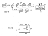
- FIG. 11 is an embodiment of the system 50' in which regulation of the feedback loop for the transistors MN1 and MN2 is performed based on voltage when the system 50' is operating in inverter mode and powering a load.
- the controller 67 generates a reference voltage waveform, VCREF, instead of a reference current waveform.
- the voltage control loop 60' compares the actual voltage VC across filtering capacitors C2, C3 and C4 to the reference voltage waveform, VCREF, and generates appropriate control signals to adjust the gate drive signals G1 and G2 for the transistors MN1 and MN2.
- the controller 67 helps ensure that the desired voltage waveform is maintained across filtering capacitors C2, C3 and C4, which in turn influences the current waveform, helping to avoid the issue of the current through Th2 failing to fall below its holding current before the zero crossing of the AC waveform.
- control loop 60 focuses on regulating the voltage across filtering capacitors C2, C3 and C4 instead of the current through inductor L2 - rather than modifying the current IL to ensure that it reaches the holding current prior to the negative half of the voltage waveform, the voltage VC is modified to ensure that the negative half of the voltage waveform does not occur prior to the current IL reaching the holding current.
- This control loop 60' is shown in FIG. 11 .
- the controller 67 generates a reference voltage waveform VCREF instead of a reference current waveform.
- the control loop 60' compares the actual voltage VC across the capacitors to the reference voltage VCREF waveform and generates appropriate control signals to adjust the gate drive signals G1 and G2 for the transistors MN1 and MN2.
- the controller 67 helps ensure that the desired voltage waveform is maintained across the filtering capacitors C2, C3 and C4, which helps avoid the issue of the current IL through Th2 failing to fall below its holding current before the zero crossing of the AC voltage waveform VC by virtue of extending the voltage waveform.
- FIG. 12 A circuit model representing the system 50 at the end of each half voltage sine wave when the transistors MN1 and MN2 are switched off is shown in FIG. 12 ; this model focuses on the filtering capacitors C2, C3 and C4 (collectively represented as Cf) and inductor L2.
- an assist voltage V ASSIST (e.g., voltage plateau) to be applied to the AC voltage waveform shortly prior to the switch-off of the transistors MN1 and MN2 at the end of each half voltage sine wave to thereby extend the period of that half voltage sine wave (so that the negative half wave does not begin until the current has fallen below the holding current) may be calculated as: V ASSIST > i AC t ASSIST ⁇ e ⁇ a ⁇ ⁇ b ⁇ T 2 ⁇ t ASSIST ⁇ DEADTIME C L ⁇ sin DEADTIME LC + 1 a ⁇ e ⁇ a ⁇ ⁇ b ⁇ T 2 ⁇ t ASSIST ⁇ DEADTIME ⁇ 1 a where L is the inductance of the inductor L2, C is the capacitance of filtering capacitors C2, C3 and C4, t ASSIST is the time between the start of the half voltage sine wave and the application of the assist voltage V ASSIST .
- a V AC RMS I PEAK ⁇ 2 1 + atan 2 ⁇
- This assist voltage V ASSIST can be observed in FIG. 13 .
Landscapes
- Engineering & Computer Science (AREA)
- Power Engineering (AREA)
- Rectifiers (AREA)
Abstract
A bidirectional PFC system includes a high-frequency branch with a first transistor connected between an IO node and a high-frequency tap, and a second transistor connected between the high-frequency tap and a reference node, and a low-frequency branch with a first thyristor connected between the IO node and a low-frequency tap, and a second thyristor connected between the low-frequency tap and the reference node. An inductor is connected between the first node and the high-frequency tap. A first capacitor is connected between the first node and the low-frequency tap. The first node and the low-frequency tap are coupled to input terminals. A control circuit generates first and second gate drive signals for the transistors so as to modify an AC signal at the input terminals such that the AC current falls below a holding current of the second thyristor prior to zero crossing of the AC voltage.
Description
- This disclosure relates generally to power electronics and, more specifically, to bidirectional totem pole power factor correction (PFC) converters with commutation assistance provided via control of the shape of the input voltage/current wave.
- Power factor correction (PFC) is technique utilized in power electronics systems to minimize the phase difference between voltage and current waveforms, in turn reducing losses in power distribution networks and enhancing the overall efficiency of the system.
- Bidirectional totem pole PFC converters are specialized devices that perform power factor correction while also providing bidirectional power flow capability. In addition to their function of power factor correction, bidirectional totem pole PFC converters can also operate in inverter mode in which the bidirectional totem pole PFC converter processes power from a DC source and generates an AC output voltage waveform suitable for supplying AC loads or injecting power into the grid.
- A conventional bidirectional
totem pole PFC 10 is shown inFIG. 1 . Thetotem pole PFC 10 includes an inductor L1 connected between a node N1 and the positive terminal of anAC source 13. The negative terminal of theAC source 13 is connected to a node N2. A filtering capacitor C is connected in parallel with theAC source 13. An n-channel transistor MN1 has its drain connected to node HVDC, its source connected to node N1, and its gate driven by a gate drive signal D1. Another n-channel transistor MN2 has its drain connected to node N1, its source connected to ground, and its gate driven by a gate drive signal D2. The n-channel transistors MN1 and MN2 form ahigh frequency branch 11. - A first thyristor Th1 has its cathode connected to node HVDC, its anode connected to node N2, and its cathode gate connected to a gate drive signal D3. A second thyristor Th2 has its cathode connected to node N2, its anode connected to ground, and its cathode gate driven by a gate drive signal D4. A third thyristor Th3 has its anode connected to node HVDC, its cathode connected to node N3, and its cathode gate driven by a gate drive signal D5. A fourth thyristor Th4 has its anode connected to node N3, its cathode connected to ground, and its cathode gate driven by a gate drive signal D6. Node N2 is connected to node N3. The thyristors Th1, Th2, Th3, and Th4 form a
low frequency branch 12. Although the thyristors are illustrated as cathode-gated devices, it will be understood that anode-gated thyristors could instead be used. - A capacitor C1 is connected between node HVDC and ground, providing energy storage and filtering for the converter. The transistors MN1 and MN2 of the high-frequency branch are responsible for shaping the current waveform to achieve the desired power factor and maintain control loop stability. The thyristors Th1, Th2, Th3, and Th4 of the low-frequency branch primarily handle the majority of the power transfer and reduce conduction losses.
- A problem arises with the conventional bidirectional
totem pole PFC 10 during the zero-crossing of the AC waveform. At the zero-crossing point, it is desired for the thyristor Th3/Th4 to be turned off, allowing the AC waveform to transition smoothly between its half-cycles. However, for a thyristor to turn off, the current through the thyristor must fall below its holding current, typically at or near zero. In the case of positive polarity, if-the current through thyristor Th4 does not fall below the holding current before the voltage waveform switches polarity, thyristor Th4 remains in the conducting state, leading to an undesired current flow. - This unintended current flow occurs when thyristor Th4 stays on during the zero-crossing of the AC waveform. The current path starts from the
AC source 13, continues to node N3, flows through thyristor Th4, returns through the ground rail, and moves through the body diode of transistor MN2 and inductor L1 before reaching theAC source 13 again. This unintended current flow can potentially cause damage to transistor MN2 and other components, affecting the overall efficiency, reliability, and performance of the bidirectional totempole PFC converter 10. - Graphs of the inductor current IL and AC waveform voltage VC across the filtering capacitor C during operation without issues are shown in
FIGS. 2-3 . In both cases, it can be observed that the inductor current IL (representative of the current through thyristor Th4) falls to zero prior to the zero-crossing of the AC waveform VC. As such, observe that the inductor current IL remains at zero during the negative portion of the AC voltage waveform. - However, in
FIG. 4 , the inductor current IL does not fall to zero prior to the zero-crossing of the AC waveform VC. As a result, the current flow situation described above occurs, and the inductor current IL rises during the negative portion of the AC voltage waveform. Since this current is flowing through the body diode of transistor MN2 as described earlier, damage may occur. - One known method to address this problem is to introduce or adjust the dead time in the control of the transistors MN1 and MN2 before the zero-crossing of the AC waveform. Dead time refers to the intentional delay between turning off of the transistors MN1 and MN2 and the reversal of the AC waveform polarity. By ceasing the switching of the transistors MN 1 and MN2, the dead time allows the current through thyristor Th4 to fall below its holding current, providing for a proper zero-crossing of the current before the reversal of the AC waveform polarity.
- A drawback of using dead time to address the zero-crossing issue is its impact on the Total Harmonic Distortion (THD), which is a measure of the distortion of the output voltage or current waveform compared to an ideal waveform. The longer the dead time, the higher the THD, as the output waveform deviates more significantly from the ideal sinusoidal shape during the non-conducting period. This increased THD can lead to diminished power quality, reduced system efficiency, and potential interference with other devices or systems connected to the same power grid and is therefore undesirable.
- Given this, a need remains for an enhanced approach to commutation assistance that improves the performance of bidirectional totem pole PFC systems, providing a smooth transition during the zero-crossing of the AC waveform without the drawbacks associated with the dead time approach described above.
- Disclosed herein is a bidirectional power factor correction system, including a high-frequency branch and a low-frequency branch. The high-frequency branch includes a first transistor connected between an IO node and a high-frequency tap, and a second transistor connected between the high-frequency tap and a reference node. The low-frequency branch includes a first thyristor connected between the IO node and a low-frequency tap, and a second thyristor connected between the low-frequency tap and the reference node. An inductor is connected between the first node and the high-frequency tap. A first capacitor is connected between the first node and the low-frequency tap. The first node and the low-frequency tap are coupled to input terminals. A control circuit is configured to generate first and second gate drive signals for the power devices of the high-frequency branch so as to modify an AC signal at the input terminals such that an AC current of the AC signal falls below a holding current of the second thyristor prior to a zero crossing of an AC voltage of the AC signal at the input terminals.
- The control circuit modifies the AC signal by either generating the first and second gate drive signals so as to accelerate a decrease of an AC current waveform at the input terminals after a peak of a half-cycle of the AC current waveform so that the AC current waveform falls below a holding current of the second thyristor prior to a zero crossing of an AC voltage waveform at the input terminals, or generating the first and second gate drive signals so as to create a plateau in an AC voltage waveform at the input terminals for a given period of time after a peak of a half-cycle of the AC voltage waveform so that the AC voltage waveform does not zero cross prior to an AC current waveform at the input terminals falls below a holding current of the second thyristor.
- The control circuit may be configured to accelerate the decrease of the AC current waveform after the peak of the half-cycle of the AC current waveform by comparing a digital reference current to a digital feedback current and generating the first and second gate drive signals based thereupon so that the digital feedback current matches the digital reference current, the digital feedback current being based upon the AC current waveform, or create the plateau in an AC voltage waveform at the input terminals for the given period of time after the peak of the half-cycle of the AC voltage waveform by generating the first and second gate drive signals to cause the first and second transistors to apply an assist voltage to the AC voltage waveform during the given period of time.
- The control circuit may be configured to create the plateau in an AC voltage waveform at the input terminals for the given period of time after the peak of the half-cycle of the AC voltage waveform by comparing a digital reference voltage to a digital feedback voltage and generating the first and second gate drive signals based thereupon so that the digital feedback voltage matches the digital reference voltage, the digital feedback voltage being based upon the AC voltage waveform.
- The control circuit may include a controller configured to generate the digital reference current based upon stored data or generate the digital reference voltage based upon stored data, a current comparator configured to generate a comparison signal based upon comparing the digital reference current to the digital feedback current or generate a comparison signal based upon comparing the digital reference voltage to the digital feedback voltage, a fast proportional-integral controller configured to generate a PWM control signal based upon the comparison signal, a pulse width modulation (PWM) circuit configured to generate gate pre-drive signals based upon the PWM control signal, a gate driving circuit configured to generate the first and second gate drive signals based upon the gate pre-drive signals, a scaling circuit configured to scale the AC current waveform to produce a scaled waveform, and an analog to digital converter configured to digitize the scaled waveform to produce the digital feedback current or the digital feedback voltage.
- The control circuit may be further configured to generate third and fourth gate drive signals for the first and second thyristors.
- Also disclosed herein is a bidirectional power factor correction system, including a high-frequency branch and a low frequency branch. The high frequency branch includes a first transistor connected between an IO node and a high-frequency tap, and a second transistor connected between the high-frequency tap and a reference node. The low-frequency branch includes a first thyristor connected between the IO node and a low-frequency tap, and a second thyristor connected between the low-frequency tap and the reference node. An inductor is connected between the first node and the high-frequency tap. A first capacitor is connected between the first node and the low-frequency tap. The first node and the low-frequency tap are coupled to input terminals. A control circuit is configured to generate first and second gate drive signals for the first and second transistors so as to accelerate a decrease of an AC current waveform at the input terminals after a peak of a half-cycle of the AC current waveform so that the AC current waveform falls below a holding current of the second thyristor prior to a zero crossing of an AC voltage waveform at the input terminals.
- The control circuit may be configured to accelerate the decrease of the AC current waveform after the peak of the half-cycle of the AC current waveform by comparing a digital reference current to a digital feedback current and generating the first and second gate drive signals based thereupon so that the digital feedback current matches the digital reference current, the digital feedback current being based upon the AC current waveform.
- The control circuit may include a controller configured to generate the digital reference current based upon stored data, a current comparator configured to generate a comparison signal based upon comparing the digital reference current to the digital feedback current, a fast proportional-integral controller configured to generate a PWM control signal based upon the comparison signal, a pulse width modulation (PWM) circuit configured to generate gate pre-drive signals based upon the PWM control signal, a gate driving circuit configured to generate the first and second gate drive signals based upon the gate pre-drive signals, a scaling circuit configured to scale the AC current waveform to produce a scaled waveform, and an analog to digital converter configured to digitize the scaled waveform to produce the digital feedback current.
- The control circuit may be further configured to generate third and fourth gate drive signals for the first and second thyristors.
- Further disclosed herein is a bidirectional power factor correction system, including a high-frequency branch and a low-frequency branch. The high-frequency branch includes a first transistor connected between an IO node and a high-frequency tap, and a second transistor connected between the high-frequency tap and a reference node. The low-frequency branch includes a first thyristor connected between the IO node and a low-frequency tap, and a second thyristor connected between the low-frequency tap and the reference node. An inductor is connected between the first node and the high-frequency tap. A first capacitor is connected between the first node and the low-frequency tap. The first node and the low-frequency tap are coupled to input terminals. A control circuit is configured to generate first and second gate drive signals for the first and second transistors so as to create a plateau in an AC voltage waveform at the input terminals for a given period of time after a peak of a half-cycle of the AC voltage waveform so that the AC voltage waveform does not zero cross prior to an AC current waveform at the input terminals falls below a holding current of the second thyristor.
- The control circuit may be configured to create the plateau in an AC voltage waveform at the input terminals for the given period of time after the peak of the half-cycle of the AC voltage waveform by generating the first and second gate drive signals to cause the first and second transistors to apply an assist voltage to the AC voltage waveform during the given period of time.
- The control circuit may be configured to create the plateau in an AC voltage waveform at the input terminals for the given period of time after the peak of the half-cycle of the AC voltage waveform by comparing a digital reference voltage to a digital feedback voltage and generating the first and second gate drive signals based thereupon so that the digital feedback voltage matches the digital reference voltage, the digital feedback voltage being based upon the AC voltage waveform.
- The control circuit may include a controller configured to generate the digital reference voltage based upon stored data, a current comparator configured to generate a comparison signal based upon comparing the digital reference voltage to the digital feedback voltage, a fast proportional-integral controller configured to generate a PWM control signal based upon the comparison signal, a pulse width modulation (PWM) circuit configured to generate gate pre-drive signals based upon the PWM control signal, a gate driving circuit configured to generate the first and second gate drive signals based upon the gate pre-drive signals, a scaling circuit configured to scale the AC voltage waveform to produce a scaled waveform, and an analog to digital converter configured to digitize the scaled waveform to produce the digital feedback voltage.
- The control circuit may be further configured to generate third and fourth gate drive signals for the first and second thyristors.
-
-
FIG. 1 is a schematic diagram of a conventional bidirectional totem pole PFC system. -
FIG. 2 is a graph illustrating the AC current waveform in the conventional bidirectional totem pole PFC system ofFIG. 1 when operating at a first current level. -
FIG. 3 is a graph illustrating the AC current waveform in the conventional bidirectional totem pole PFC system ofFIG. 1 when operating at a second current level. -
FIG. 4 is a graph illustrating the AC current waveform in the conventional bidirectional totem pole PFC system ofFIG. 1 when operating at a third current level. -
FIG. 5 is a schematic diagram of a bidirectional totem pole PFC system disclosed herein. -
FIG. 6 is a block diagram of a first control loop for the system ofFIG. 5 disclosed herein. -
FIG. 7 is a circuit model of the system ofFIG. 5 in a condition in which transistors are turned off before the reversal of the AC waveform polarity. -
FIG. 8 is a series of graphs showing the relationship between the safety margin ofFIG. 5 in operation and the holding current and dead time. -
FIG. 9 is a series of graphs showing a comparison between the potential generated reference currents inFIG. 5 and a prior art reference current. -
FIG. 10 is a graph showing the effect of the first control loop ofFIG. 6 on the AC current waveform. -
FIG. 11 is a block diagram of a second control loop for the system ofFIG. 5 disclosed herein. -
FIG. 12 is a circuit model of the system ofFIG. 5 at the peak of the positive half wave of the AC voltage waveform. -
FIG. 13 is a graph showing the effect of the application of the assist voltage to the AC voltage waveform ofFIG. 5 . - The following disclosure enables a person skilled in the art to make and use the subject matter described herein. The general principles outlined in this disclosure can be applied to embodiments and applications other than those detailed above without departing from the spirit and scope of this disclosure. It is not intended to limit this disclosure to the embodiments shown, but to accord it the widest scope consistent with the principles and features disclosed or suggested herein.
- Note that in the following description, any resistor or resistance mentioned is a discrete device, unless stated otherwise, and is not simply an electrical lead between two points. Therefore, any resistor or resistance connected between two points has a higher resistance than a lead between those two points, and such resistor or resistance cannot be interpreted as a lead. Similarly, any capacitor or capacitance mentioned is a discrete device, unless stated otherwise, and is not a parasitic element, unless stated otherwise. Additionally, any inductor or inductance mentioned is a discrete device, unless stated otherwise, and is not a parasitic element, unless stated otherwise.
- Now described with reference to
FIG. 5 is a bidirectional totempole PFC system 50 including an enhanced approach to commutation assistance. The totempole PFC system 50 includes ahigh frequency branch 51 andlow frequency branch 52 connected between node HVDC and ground. Thehigh frequency branch 51 is formed by an n-channel transistor MN1 having its drain connected to node HVDC, its source connected to node Nn7, and its gate coupled to be controlled by a gate drive signal G1, and an n-channel transistor MN2 having its drain connected to node Nn7, its source connected to ground, and its gate coupled to be controlled by gate drive signal G2. Thelow frequency branch 52 is formed by a first thyristor Th1 having its anode connected to node HVDC, its cathode connected to node Nn8, and its cathode gate coupled to be controlled by gate drive signal G3, and a second thyristor Th2 having its anode connected to node Nn8, its cathode connected to ground, and its cathode gate coupled to be controlled by gate drive signal G4. A capacitor C5 is connected between node HVDC and ground. Although the thyristors are illustrated as cathode-gated devices, it will be understood that anode-gated thyristors could instead be used. - An inductor L2 is connected between notes Nn7 and Nn6. A bypass diode Dd1 has its cathode connected to node HVDC and its anode connected to node Nn6, while a bypass diode Dd2 has its cathode connected to node Nn6 and its anode connected to ground.
- An
AC source 13 has its positive terminal connected to node Nn1 and its negative terminal connected to a second terminal of a capacitor C2. The second terminal of the resistor R2 and the first terminal of the capacitor C2 are connected to node Nn1. A common mode inductor T1 has its primary winding connected between nodes Nn1 and Nn2 and has its secondary winding connected between the negative terminal of theAC source 13 and node Nn3. A common mode inductor T2 has its primary winding connected between nodes Nn2 and Nn4 and its secondary winding connected between nodes Nn3 and Nn5. A capacitor C3 is connected between nodes Nn4 and Nn5. A common mode inductor T3 has its primary winding connected between nodes Nn4 and Nn6 and its secondary winding connected between nodes Nn5 and Nn8. A capacitor C4 is connected between nodes Nn6 and Nn8. - The common mode inductor T1, T2, and T3 and the capacitors C2, C3, and C4 serve various functions within the bidirectional totem
pole PFC system 50, such as filtration, noise protection, and smoothing of voltage waveforms across the thyristors Th1 and Th2. - Recall the potential issue of the current through the thyristor Th1/Th2 failing to fall below the holding current before the switching of the AC voltage waveform. In order to address this, two approaches can be considered: modifying the AC current waveform or modifying the AC voltage waveform. Both methods involve making adjustments in the control of transistors MN1 and MN2.
- First, the modification of the AC current waveform will be discussed in the context of which the
system 50 is operating in inverter mode and providing power to the grid. In the embodiment illustrated inFIG. 6 , thefirst control loop 60 generates the gate drive signals G1 and G2 to control the transistors MN1 and MN2, and asecond control loop 70 generates the gate drive signals G3 and G4 for the thyristors Th1 and Th2. - The
first control loop 60 includes acurrent comparator 61, which receives as input a reference current ILREF (a digital value representing the desired AC current level, generated by acontroller 67 based upon a stored table) and a feedback current IFBK (a digital value representing the actual inductor current IL). The output of thecurrent comparator 61 is provided to a fast proportional-integral (PI)controller 62. ThePI controller 62 adjusts the control signal Ctrl it outputs based on the output of thecurrent comparator 61, i.e., based on the error between the reference current ILREF and the feedback current IFBK. ThePI controller 62 quickly responds to changes in the actual inductor current IL, which is used to generate the feedback current IFBK. The control signal Ctrl is received by a pulse width modulation (PWM)generator 63, which generates appropriate switching signals for the transistors MN1 and MN2. These switching signals are received by agate driver 64 for the transistors MN1 and MN2, which drives the transistors MN1 and MN2 accordingly. To close the loop, the inductor current IL is received through a current scaling block (KI) 65, which senses and scales the inductor current IL (ILSNS being the sensed current) by a scaling factor K. The scaled inductor current is then digitized by an analog-to-digital converter (ADC) 66 to produce the feedback current IFBK. - Generation of the table stored in the
controller 67 and used to generate the reference current ILREF is now described. Refer to the model of the bidirectional totempole PFC system 50 shown inFIG. 7 . This model represents the current path that would occur when the transistors MN1 and MN2 are turned off before the zero crossing of the AC waveform. Note that the diode labeled MN2BD represents the body diode of transistor MN2, and that theAC source 13 here is represented as a current source. Current IL represents the current through the inductor L2, current IC represents the current into the filtering capacitors C2, C3 and C4 (collectively labeled as capacitor Cf inFIG. 7 ), and current ILine represents the current returning to theAC source 13. - Keeping this in mind, the voltage vC , the voltage across filtering capacitors C2, C3 and C4, can be calculated as:

- The current iL through the inductor L2 can be calculated as:


- The value µ can be calculated as:


- The value λ can be calculated as :

- Using the equations derived for vC (t) and iL (t), as well as the calculated values of λ and µ, the
controller 67 can determine the appropriate reference current waveform shape to avoid the issue of the current through Th2 failing to fall below its holding current before the zero crossing of the AC waveform. By adjusting the gate drive signals G1 and G2 for the transistors MN1 and MN2 based on the analysis of the mathematical model and determination of the values of λ and µ, thecontroller 67 can control the AC current waveform such that the current experiences an accelerated decrease towards the end of the half-cycle and maintains a zero current level for a small duration, known as the dead time. - The
controller 67 creates a table containing the reference current values that correspond to the desired current waveform shape, taking into account a chosen safety margin ΔT. The safety margin ΔT is the time between the AC current hitting zero and the AC voltage hitting zero, and it is determined based on the desired dead time and the holding current of the thyristor Th2. A greater safety margin provides more time for the current through Th2 to fall below its holding current, providing for a more reliable turn-off, while a smaller safety margin allows for a faster transition to the negative portion of the AC voltage waveform, potentially improving overall efficiency. The effect of dead time and holding current on the safety margin ΔT can be observed inFIG. 8 - observe that the safety margin ΔT decreases as the current increases for example. - Therefore, the safety margin ΔT is appropriately chosen to provide for reliable operation while helping to minimize total harmonic distortion (THD) so that the system can achieve stable and efficient performance with low impact on power quality. The safety margin ΔT is therefore chosen to be as small as possible while still providing a sufficient buffer (to account for transients, non-ideality in the transistors, etc.) for the current through Th2 to fall below its holding current before the negative portion of the AC voltage waveform.
- Once the table is generated, it is stored within the
controller 67. The controller then uses this table to generate the reference current ILREF during the operation of the bidirectional totempole PFC system 50. The reference current ILREF is input to thecurrent comparator 61, where it is compared with the feedback current IFBK, and the error between them is used by the fast proportional-integral (PI)controller 62 to adjust the control signal Ctrl. This control signal is then used by thePWM generator 63 to produce appropriate switching signals for the transistors MN1 and MN2, allowing the system to achieve the desired current waveform shape with the adjusted safety margin ΔT. - By implementing this technique, the bidirectional totem
pole PFC system 50 can effectively control the AC current waveform to help ensure that Th2 turns off before the negative portion of the AC waveform, providing for efficient and stable operation of the system. - In some embodiments, multiple such tables may be stored within the
controller 67. For example, a first table suitable for generating a reference current Ilow suitable for use in a low voltage application (e.g., a grid voltage of 110 V) and a second table suitable for generating a reference current Ihigh suitable for use in a high voltage application (e.g., a grid voltage of 220 V), as shown inFIG. 9 . Both of these are shown as compared to a conventional reference current Istd in which the period of the AC waveform does not experience an accelerated decrease towards the end of the positive and negative half-cycle. - The inductor current IL generated using this current control technique as compared to a conventionally generated inductor current ILREG and the capacitor voltage VC can be observed in
FIG. 10 . Note that while the currents IL and ILREG have the same waveform shape up until the peak current, after that peak is reached, current IL experiences an accelerated decrease towards the end of the half-cycle. - Now described with reference to
FIG. 11 is an embodiment of the system 50' in which regulation of the feedback loop for the transistors MN1 and MN2 is performed based on voltage when the system 50' is operating in inverter mode and powering a load. In this case, thecontroller 67 generates a reference voltage waveform, VCREF, instead of a reference current waveform. The voltage control loop 60' compares the actual voltage VC across filtering capacitors C2, C3 and C4 to the reference voltage waveform, VCREF, and generates appropriate control signals to adjust the gate drive signals G1 and G2 for the transistors MN1 and MN2. By doing so, thecontroller 67 helps ensure that the desired voltage waveform is maintained across filtering capacitors C2, C3 and C4, which in turn influences the current waveform, helping to avoid the issue of the current through Th2 failing to fall below its holding current before the zero crossing of the AC waveform. - The underlying principle of controlling the current decay and incorporating a safety margin is similar to the previous embodiment. The main difference is that the control loop focuses on regulating the voltage across filtering capacitors C2, C3 and C4 instead of the current through inductor L2 - rather than modifying the current IL to ensure that it reaches the holding current prior to the negative half of the voltage waveform, the voltage VC is modified to ensure that the negative half of the voltage waveform does not occur prior to the current IL reaching the holding current. This control loop 60' is shown in
FIG. 11 . - In this case, the
controller 67 generates a reference voltage waveform VCREF instead of a reference current waveform. The control loop 60' compares the actual voltage VC across the capacitors to the reference voltage VCREF waveform and generates appropriate control signals to adjust the gate drive signals G1 and G2 for the transistors MN1 and MN2. By doing so, thecontroller 67 helps ensure that the desired voltage waveform is maintained across the filtering capacitors C2, C3 and C4, which helps avoid the issue of the current IL through Th2 failing to fall below its holding current before the zero crossing of the AC voltage waveform VC by virtue of extending the voltage waveform. - A circuit model representing the
system 50 at the end of each half voltage sine wave when the transistors MN1 and MN2 are switched off is shown inFIG. 12 ; this model focuses on the filtering capacitors C2, C3 and C4 (collectively represented as Cf) and inductor L2. Here, an assist voltage VASSIST (e.g., voltage plateau) to be applied to the AC voltage waveform shortly prior to the switch-off of the transistors MN1 and MN2 at the end of each half voltage sine wave to thereby extend the period of that half voltage sine wave (so that the negative half wave does not begin until the current has fallen below the holding current) may be calculated as:
- The value a can be calculated as:

- The value b can be calculated as :

- This assist voltage VASSIST can be observed in
FIG. 13 . - All or part of the disclosed embodiments can be summarized by the following examples.
- Example 1. A bidirectional power factor correction system, comprising:
- a high-frequency branch comprising: a first transistor connected between an IO node and a high-frequency tap, and a second transistor connected between the high-frequency tap and a reference node;
- a low-frequency branch comprising: a first thyristor connected between the IO node and a low-frequency tap, and a second thyristor connected between the low-frequency tap and the reference node;
- an inductor connected between the first node and the high-frequency tap;
- a first capacitor connected between the first node and the low-frequency tap;
- wherein the first node and the low-frequency tap are coupled to input terminals;
- a control circuit configured to generate first and second gate drive signals for the power devices of the high-frequency branch so as to modify an AC signal at the input terminals such that an AC current of the AC signal falls below a holding current of the second thyristor prior to a zero crossing of an AC voltage of the AC signal at the input terminals;
- wherein the control circuit modifies the AC signal by either:
- generating the first and second gate drive signals so as to accelerate a decrease of an AC current waveform at the input terminals after a peak of a half-cycle of the AC current waveform so that the AC current waveform falls below a holding current of the second thyristor prior to a zero crossing of an AC voltage waveform at the input terminals; or
- generating the first and second gate drive signals so as to create a plateau in an AC voltage waveform at the input terminals for a given period of time after a peak of a half-cycle of the AC voltage waveform so that the AC voltage waveform does not zero cross prior to an AC current waveform at the input terminals falls below a holding current of the second thyristor.
- Example 2. The bidirectional power factor correction system of example 1, wherein the control circuit is configured to:
- accelerate the decrease of the AC current waveform after the peak of the half-cycle of the AC current waveform by comparing a digital reference current to a digital feedback current and generating the first and second gate drive signals based thereupon so that the digital feedback current matches the digital reference current, the digital feedback current being based upon the AC current waveform; or
- create the plateau in an AC voltage waveform at the input terminals for the given period of time after the peak of the half-cycle of the AC voltage waveform by generating the first and second gate drive signals to cause the first and second transistors to apply an assist voltage to the AC voltage waveform during the given period of time.
- Example 3. The bidirectional power factor correction system of example 2, wherein the control circuit is configured to create the plateau in an AC voltage waveform at the input terminals for the given period of time after the peak of the half-cycle of the AC voltage waveform by comparing a digital reference voltage to a digital feedback voltage and generating the first and second gate drive signals based thereupon so that the digital feedback voltage matches the digital reference voltage, the digital feedback voltage being based upon the AC voltage waveform.
- Example 4. The bidirectional power factor correction system of example 2 or 3, wherein the control circuit comprises:
- a controller configured to: generate the digital reference current based upon stored data or generate the digital reference voltage based upon stored data;
- a current comparator configured to generate a comparison signal based upon: comparing the digital reference current to the digital feedback current or generate a comparison signal based upon comparing the digital reference voltage to the digital feedback voltage;
- a fast proportional-integral controller configured to generate a PWM control signal based upon the comparison signal;
- a pulse width modulation (PWM) circuit configured to generate gate pre-drive signals based upon the PWM control signal;
- a gate driving circuit configured to generate the first and second gate drive signals based upon the gate pre-drive signals;
- a scaling circuit configured to scale the AC current waveform to produce a scaled waveform; and
- an analog to digital converter configured to digitize the scaled waveform to produce the digital feedback current or the digital feedback voltage.
- Example 5. The bidirectional power factor correction system of any of examples 1 to 4, wherein the control circuit is further configured to generate third and fourth gate drive signals for the first and second thyristors.
- Example 6. A bidirectional power factor correction system, comprising:
- a high-frequency branch comprising: a first transistor connected between an IO node and a high-frequency tap, and a second transistor connected between the high-frequency tap and a reference node;
- a low-frequency branch comprising: a first thyristor connected between the IO node and a low-frequency tap, and a second thyristor connected between the low-frequency tap and the reference node;
- an inductor connected between the first node and the high-frequency tap;
- a first capacitor connected between the first node and the low-frequency tap;
- wherein the first node and the low-frequency tap are coupled to input terminals; and
- a control circuit configured to generate first and second gate drive signals for the first and second transistors so as to accelerate a decrease of an AC current waveform at the input terminals after a peak of a half-cycle of the AC current waveform so that the AC current waveform falls below a holding current of the second thyristor prior to a zero crossing of an AC voltage waveform at the input terminals.
- Example 7. The bidirectional power factor correction system of example 6, wherein the control circuit is configured to accelerate the decrease of the AC current waveform after the peak of the half-cycle of the AC current waveform by comparing a digital reference current to a digital feedback current and generating the first and second gate drive signals based thereupon so that the digital feedback current matches the digital reference current, the digital feedback current being based upon the AC current waveform.
- Example 8. The bidirectional power factor correction system of example 7, wherein the control circuit comprises:
- a controller configured to generate the digital reference current based upon stored data;
- a current comparator configured to generate a comparison signal based upon comparing the digital reference current to the digital feedback current;
- a fast proportional-integral controller configured to generate a PWM control signal based upon the comparison signal;
- a pulse width modulation (PWM) circuit configured to generate gate pre-drive signals based upon the PWM control signal;
- a gate driving circuit configured to generate the first and second gate drive signals based upon the gate pre-drive signals;
- a scaling circuit configured to scale the AC current waveform to produce a scaled waveform; and
- an analog to digital converter configured to digitize the scaled waveform to produce the digital feedback current.
- Example 9. The bidirectional power factor correction system of any of examples 6 to 8, wherein the control circuit is further configured to generate third and fourth gate drive signals for the first and second thyristors.
- Example 10. A bidirectional power factor correction system, comprising:
- a high-frequency branch comprising: a first transistor connected between an IO node and a high-frequency tap, and a second transistor connected between the high-frequency tap and a reference node;
- a low-frequency branch comprising: a first thyristor connected between the IO node and a low-frequency tap; and a second thyristor connected between the low-frequency tap and the reference node;
- an inductor connected between the first node and the high-frequency tap;
- a first capacitor connected between the first node and the low-frequency tap;
- wherein the first node and the low-frequency tap are coupled to input terminals; and
- a control circuit configured to generate first and second gate drive signals for the first and second transistors so as to create a plateau in an AC voltage waveform at the input terminals for a given period of time after a peak of a half-cycle of the AC voltage waveform so that the AC voltage waveform does not zero cross prior to an AC current waveform at the input terminals falls below a holding current of the second thyristor.
- Example 11. The bidirectional power factor correction system of example 10, wherein the control circuit is configured to create the plateau in an AC voltage waveform at the input terminals for the given period of time after the peak of the half-cycle of the AC voltage waveform by generating the first and second gate drive signals to cause the first and second transistors to apply an assist voltage to the AC voltage waveform during the given period of time.
- Example 12. The bidirectional power factor correction system of example 11, wherein the control circuit is configured to create the plateau in an AC voltage waveform at the input terminals for the given period of time after the peak of the half-cycle of the AC voltage waveform by comparing a digital reference voltage to a digital feedback voltage and generating the first and second gate drive signals based thereupon so that the digital feedback voltage matches the digital reference voltage, the digital feedback voltage being based upon the AC voltage waveform.
- Example 13. The bidirectional power factor correction system of example 12, wherein the control circuit comprises:
- a controller configured to generate the digital reference voltage based upon stored data;
- a current comparator configured to generate a comparison signal based upon comparing the digital reference voltage to the digital feedback voltage;
- a fast proportional-integral controller configured to generate a PWM control signal based upon the comparison signal;
- a pulse width modulation (PWM) circuit configured to generate gate pre-drive signals based upon the PWM control signal;
- a gate driving circuit configured to generate the first and second gate drive signals based upon the gate pre-drive signals;
- a scaling circuit configured to scale the AC voltage waveform to produce a scaled waveform; and
- an analog to digital converter configured to digitize the scaled waveform to produce the digital feedback voltage.
- Example 14. The bidirectional power factor correction system of any of examples 10 to 13, wherein the control circuit is further configured to generate third and fourth gate drive signals for the first and second thyristors.
- Example 15. A bidirectional power factor correction system, comprising:
- a high-frequency branch comprising: a first transistor connected between an IO node and a high-frequency tap, and a second transistor connected between the high-frequency tap and a reference node;
- a low-frequency branch comprising: a first thyristor connected between the IO node and a low-frequency tap, and a second thyristor connected between the low-frequency tap and the reference node;
- an inductor connected between the first node and the high-frequency tap;
- a first capacitor connected between the first node and the low-frequency tap;
- wherein the first node and the low-frequency tap are coupled to input terminals;
- a control circuit configured to generate first and second gate drive signals for the power devices of the high-frequency branch so as to modify an AC signal at the input terminals such that an AC current of the AC signal falls below a holding current of the second thyristor prior to a zero crossing of an AC voltage of the AC signal at the input terminals.
- Example 16. The bidirectional power factor correction system of example 15, wherein the control circuit modifies the AC signal by generating the first and second gate drive signals so as to change the AC signal at the input terminals after a peak of a half-cycle thereof.
- Example 17. The bidirectional power factor correction system of example 16, wherein the control circuit modifies the AC signal based upon a comparison between a digital reference and a digital feedback based upon the AC signal.
- Example 18. The bidirectional power factor correction system of example 17, wherein the digital reference is a digital reference current and the digital feedback is a digital feedback current.
- Example 19. The bidirectional power factor correction system of example 17, wherein the digital reference is a digital reference voltage and the digital feedback is a digital feedback voltage.
- It is evident that modifications and variations can be made to what has been described and illustrated herein without departing from the scope of this disclosure.
- Although this disclosure has been described with a limited number of embodiments, those skilled in the art, having the benefit of this disclosure, can envision other embodiments that do not deviate from the disclosed scope. Furthermore, skilled persons can envision embodiments that represent various combinations of the embodiments disclosed herein made in various ways.
Claims (14)
- A bidirectional power factor correction system, comprising:a high-frequency branch comprising: a first transistor connected between an IO node and a high-frequency tap, and a second transistor connected between the high-frequency tap and a reference node;a low-frequency branch comprising: a first thyristor connected between the IO node and a low-frequency tap, and a second thyristor connected between the low-frequency tap and the reference node;an inductor connected between the first node and the high-frequency tap;a first capacitor connected between the first node and the low-frequency tap;wherein the first node and the low-frequency tap are coupled to input terminals;a control circuit configured to generate first and second gate drive signals for the first and second transistors of the high-frequency branch so as to modify an AC signal at the input terminals.
- The bidirectional power factor correction system of claim 1, wherein the control circuit is configured to modify said AC signal at the input terminal such that an AC current of the AC signal falls below a holding current of the second thyristor prior to a zero crossing of an AC voltage of the AC signal at the input terminals.
- The bidirectional power factor correction system of claim 1 or 2, wherein the control circuit modifies the AC signal by generating the first and second gate drive signals so as to change the AC signal at the input terminals after a peak of a half-cycle thereof.
- The bidirectional power factor correction system of any of claims 1 to 3, wherein the control circuit modifies the AC signal based upon a comparison between a digital reference and a digital feedback based upon the AC signal.
- The bidirectional power factor correction system of claim 4, wherein the control circuit comprises:a controller configured to: generate the digital reference current based upon stored data or generate the digital reference voltage based upon stored data;a current comparator configured to generate a comparison signal based upon: comparing the digital reference current to the digital feedback current or generate a comparison signal based upon comparing the digital reference voltage to the digital feedback voltage;a fast proportional-integral controller configured to generate a PWM control signal based upon the comparison signal;a pulse width modulation (PWM) circuit configured to generate gate pre-drive signals based upon the PWM control signal;a gate driving circuit configured to generate the first and second gate drive signals based upon the gate pre-drive signals;a scaling circuit configured to scale the AC current waveform to produce a scaled waveform; andan analog to digital converter configured to digitize the scaled waveform to produce the digital feedback current or the digital feedback voltage.
- The bidirectional power factor correction system of any of claims 1 to 5, wherein the control circuit is configured to generate the first and second gate drive signals so as to accelerate a decrease of an AC current waveform at the input terminals after a peak of a half-cycle of the AC current waveform so that the AC current waveform falls below a holding current of the second thyristor prior to a zero crossing of an AC voltage waveform at the input terminals.
- The bidirectional power factor correction system of claim 6, in its dependency on claim 4 or 5, wherein the digital reference is a digital reference current and the digital feedback is a digital feedback current.
- The bidirectional power factor correction system of claim 7, wherein the control circuit is configured to accelerate the decrease of the AC current waveform after the peak of the half-cycle of the AC current waveform by comparing said digital reference current to said digital feedback current and generating the first and second gate drive signals based thereupon so that the digital feedback current matches the digital reference current, the digital feedback current being based upon the AC current waveform.
- The bidirectional power factor correction system of any of claims 1 to 5, wherein the control circuit is configured to generate the first and second gate drive signals so as to create a plateau in an AC voltage waveform at the input terminals for a given period of time after a peak of a half-cycle of the AC voltage waveform so that the AC voltage waveform does not zero cross prior to an AC current waveform at the input terminals falls below a holding current of the second thyristor.
- The bidirectional power factor correction system of claim 9, wherein the control circuit is configured to create the plateau in an AC voltage waveform at the input terminals for the given period of time after the peak of the half-cycle of the AC voltage waveform by generating the first and second gate drive signals to cause the first and second transistors to apply an assist voltage to the AC voltage waveform during the given period of time.
- The bidirectional power factor correction system of claim 9 or 10, in their dependency on claim 4 or 5, wherein the digital reference is a digital reference voltage and the digital feedback is a digital feedback voltage.
- The bidirectional power factor correction system of claim 11, wherein the control circuit is configured to create the plateau in an AC voltage waveform at the input terminals for the given period of time after the peak of the half-cycle of the AC voltage waveform by comparing a digital reference voltage to a digital feedback voltage and generating the first and second gate drive signals based thereupon so that the digital feedback voltage matches the digital reference voltage, the digital feedback voltage being based upon the AC voltage waveform.
- The bidirectional power factor correction system of claim 1, wherein the control circuit is configured to modify the AC signal at the input terminal either according to any of claims 6 to 8 or according to any of claims 9 to 12.
- The bidirectional power factor correction system of any claims 1 to 13, wherein the control circuit is further configured to generate third and fourth gate drive signals for the first and second thyristors.
Applications Claiming Priority (1)
| Application Number | Priority Date | Filing Date | Title |
|---|---|---|---|
| US18/203,299 US12362662B2 (en) | 2023-05-30 | 2023-05-30 | Commutation assistance by controlling the shape of the current wave in a bidirectional totem pole converter |
Publications (1)
| Publication Number | Publication Date |
|---|---|
| EP4472050A1 true EP4472050A1 (en) | 2024-12-04 |
Family
ID=91699911
Family Applications (1)
| Application Number | Title | Priority Date | Filing Date |
|---|---|---|---|
| EP24315250.1A Pending EP4472050A1 (en) | 2023-05-30 | 2024-05-29 | Commutation assistance by controlling the shape of the current wave in a bidirectional totem pole converter |
Country Status (3)
| Country | Link |
|---|---|
| US (2) | US12362662B2 (en) |
| EP (1) | EP4472050A1 (en) |
| CN (1) | CN119070622A (en) |
Families Citing this family (1)
| Publication number | Priority date | Publication date | Assignee | Title |
|---|---|---|---|---|
| US12609600B2 (en) * | 2023-06-29 | 2026-04-21 | Infineon Technologies Austria Ag | Method and apparatus for estimating voltage regulator current |
Family Cites Families (14)
| Publication number | Priority date | Publication date | Assignee | Title |
|---|---|---|---|---|
| EP2871760B1 (en) | 2013-11-08 | 2018-03-21 | DET International Holding Limited | Resistorless precharging |
| FR3034924A1 (en) | 2015-04-07 | 2016-10-14 | St Microelectronics Tours Sas | ALTERNATIVE-CONTINUOUS CONVERTER WITH CURRENT CURRENT LIMITATION |
| FR3037741A1 (en) | 2015-06-22 | 2016-12-23 | St Microelectronics Tours Sas | POWER FACTOR CORRECTING CIRCUIT CONVERTER |
| FR3068547B1 (en) | 2017-06-30 | 2019-08-16 | Stmicroelectronics (Tours) Sas | THYRISTORS REVERSIBLE AC / DC CONVERTER |
| FR3068546B1 (en) | 2017-06-30 | 2020-12-11 | St Microelectronics Tours Sas | REVERSIBLE AC / DC CONVERTER TO TRIACS |
| US11251696B2 (en) | 2019-05-31 | 2022-02-15 | Stmicroelectronics Ltd | Discharge of an AC capacitor |
| FR3097089B1 (en) | 2019-06-07 | 2022-03-25 | Valeo Siemens Eautomotive France Sas | A CONVERTER AND ITS CURRENT CONTROL SYSTEM |
| JP2021002983A (en) * | 2019-06-24 | 2021-01-07 | ルネサスエレクトロニクス株式会社 | Semiconductor device |
| FR3102897B1 (en) | 2019-10-30 | 2021-11-12 | St Microelectronics Tours Sas | Bridge rectifier |
| US11228239B2 (en) * | 2020-04-27 | 2022-01-18 | Stmicroelectronics (Tours) Sas | Discharge of an AC capacitor using totem-pole power factor correction (PFC) circuitry |
| JP7518596B2 (en) | 2021-02-10 | 2024-07-18 | パナソニックオートモーティブシステムズ株式会社 | Switching Power Supply Unit |
| FR3122793B1 (en) | 2021-05-07 | 2024-09-27 | St Microelectronics Ltd | Electronic circuit with thyristor |
| FR3126823A1 (en) | 2021-09-08 | 2023-03-10 | Stmicroelectronics (Tours) Sas | voltage converter |
| CN113726135A (en) | 2021-09-24 | 2021-11-30 | 桂林电子科技大学 | Silicon controlled switch circuit switched off by shunting of MOS (metal oxide semiconductor) tube |
-
2023
- 2023-05-30 US US18/203,299 patent/US12362662B2/en active Active
-
2024
- 2024-05-28 CN CN202410668638.6A patent/CN119070622A/en active Pending
- 2024-05-29 EP EP24315250.1A patent/EP4472050A1/en active Pending
-
2025
- 2025-06-23 US US19/246,311 patent/US20250317051A1/en active Pending
Non-Patent Citations (3)
| Title |
|---|
| JING LEI ET AL: "An Optimized Control Strategy to Improve the Current Zero-Crossing Distortion in Bidirectional AC/DC Converter based on V2G Concept", 2018 INTERNATIONAL POWER ELECTRONICS CONFERENCE (IPEC-NIIGATA 2018 -ECCE ASIA), IEEJ INDUSTRY APPLICATION SOCIETY, 20 May 2018 (2018-05-20), pages 878 - 882, XP033426635, DOI: 10.23919/IPEC.2018.8507917 * |
| TRANSPHORM: "TDTTP3300-RD 3.3kW Bridgeless Totem-pole PFC", 28 February 2018 (2018-02-28), pages 1 - 24, XP093214244, Retrieved from the Internet <URL:https://www.transphormusa.com/en/document/tdttp3300-rd-reference-design-firmware-guide/> [retrieved on 20241011] * |
| VU TRONG TUE ET AL: "99% Efficiency 3-Level Bridgeless Totem-pole PFC Implementation with Low-voltage Silicon at Low Cost", 2019 IEEE APPLIED POWER ELECTRONICS CONFERENCE AND EXPOSITION (APEC), IEEE, 17 March 2019 (2019-03-17), pages 2077 - 2083, XP033556000, DOI: 10.1109/APEC.2019.8721928 * |
Also Published As
| Publication number | Publication date |
|---|---|
| CN119070622A (en) | 2024-12-03 |
| US20240405670A1 (en) | 2024-12-05 |
| US12362662B2 (en) | 2025-07-15 |
| US20250317051A1 (en) | 2025-10-09 |
Similar Documents
| Publication | Publication Date | Title |
|---|---|---|
| US10686362B2 (en) | Variable delay for soft switching in power conversion circuit | |
| US10141868B2 (en) | Method and apparatus for resonant power conversion | |
| US9407156B2 (en) | Managing leakage inductance in a power supply | |
| CN102246404B (en) | Power conversion device | |
| US11736031B2 (en) | Unfolder-based single-stage AC-AC conversion system | |
| JP4850279B2 (en) | Power converter | |
| JP6196949B2 (en) | Power converter | |
| US11929669B2 (en) | Totem-pole bridgeless power factor correction device and power supply | |
| Guo et al. | Three-level bidirectional DC–DC converter with an auxiliary inductor in adaptive working mode for full-operation zero-voltage switching | |
| CN102379081A (en) | Power conversion device | |
| US20250317051A1 (en) | Commutation assistance by controlling the shape of the current wave in a bidirectional totem pole converter | |
| US20240178739A1 (en) | Control apparatus for an arcp inverter | |
| CN119182272A (en) | Device for current sharing of parallel-connected converters | |
| JP5169017B2 (en) | Power converter | |
| Liu et al. | Adaptive soft switching asymmetrical half bridge flyback converter with wider voltage range | |
| JP5043585B2 (en) | Power converter | |
| JP2015228760A (en) | Switching power supply | |
| Tayebi et al. | Effects of circuit nonlinearities on dynamic dead time optimization for a three-phase microinverter | |
| JP7561688B2 (en) | Power Conversion Equipment | |
| CN117318475A (en) | Energy storage converter and control method, device and readable storage medium thereof | |
| US10135351B2 (en) | Circuit and method for AC-to-AC voltage conversion | |
| Wang et al. | Digital ZVS BCM current controlled single-phase full-bridge inverter using DSP TMS320F28035 | |
| US20240283376A1 (en) | Apparatus and method for bi-directional ac/dc power conversion | |
| Yang et al. | High-efficiency three-level SEPIC for grid-tied PV systems | |
| Sheng et al. | Fundamental Frequency Modulation with Dead-Time Compensation for Suppressing Surge Voltage in Modular Multilevel Resonant DC-DC Converters |
Legal Events
| Date | Code | Title | Description |
|---|---|---|---|
| PUAI | Public reference made under article 153(3) epc to a published international application that has entered the european phase |
Free format text: ORIGINAL CODE: 0009012 |
|
| STAA | Information on the status of an ep patent application or granted ep patent |
Free format text: STATUS: REQUEST FOR EXAMINATION WAS MADE |
|
| 17P | Request for examination filed |
Effective date: 20240529 |
|
| AK | Designated contracting states |
Kind code of ref document: A1 Designated state(s): AL AT BE BG CH CY CZ DE DK EE ES FI FR GB GR HR HU IE IS IT LI LT LU LV MC ME MK MT NL NO PL PT RO RS SE SI SK SM TR |