EP4471830A1 - Josephson element, superconducting circuit, quantum computation device, and method for manufacturing josephson element - Google Patents
Josephson element, superconducting circuit, quantum computation device, and method for manufacturing josephson element Download PDFInfo
- Publication number
- EP4471830A1 EP4471830A1 EP22921936.5A EP22921936A EP4471830A1 EP 4471830 A1 EP4471830 A1 EP 4471830A1 EP 22921936 A EP22921936 A EP 22921936A EP 4471830 A1 EP4471830 A1 EP 4471830A1
- Authority
- EP
- European Patent Office
- Prior art keywords
- metal layer
- superconducting metal
- superconducting
- substrate
- layer
- Prior art date
- Legal status (The legal status is an assumption and is not a legal conclusion. Google has not performed a legal analysis and makes no representation as to the accuracy of the status listed.)
- Granted
Links
Images


























Classifications
-
- H—ELECTRICITY
- H10—SEMICONDUCTOR DEVICES; ELECTRIC SOLID-STATE DEVICES NOT OTHERWISE PROVIDED FOR
- H10N—ELECTRIC SOLID-STATE DEVICES NOT OTHERWISE PROVIDED FOR
- H10N60/00—Superconducting devices
- H10N60/01—Manufacture or treatment
- H10N60/0912—Manufacture or treatment of Josephson-effect devices
-
- G—PHYSICS
- G06—COMPUTING OR CALCULATING; COUNTING
- G06N—COMPUTING ARRANGEMENTS BASED ON SPECIFIC COMPUTATIONAL MODELS
- G06N10/00—Quantum computing, i.e. information processing based on quantum-mechanical phenomena
- G06N10/40—Physical realisations or architectures of quantum processors or components for manipulating qubits, e.g. qubit coupling or qubit control
-
- H—ELECTRICITY
- H10—SEMICONDUCTOR DEVICES; ELECTRIC SOLID-STATE DEVICES NOT OTHERWISE PROVIDED FOR
- H10N—ELECTRIC SOLID-STATE DEVICES NOT OTHERWISE PROVIDED FOR
- H10N60/00—Superconducting devices
- H10N60/10—Junction-based devices
- H10N60/12—Josephson-effect devices
-
- H—ELECTRICITY
- H10—SEMICONDUCTOR DEVICES; ELECTRIC SOLID-STATE DEVICES NOT OTHERWISE PROVIDED FOR
- H10N—ELECTRIC SOLID-STATE DEVICES NOT OTHERWISE PROVIDED FOR
- H10N60/00—Superconducting devices
- H10N60/80—Constructional details
- H10N60/805—Constructional details for Josephson-effect devices
-
- H—ELECTRICITY
- H10—SEMICONDUCTOR DEVICES; ELECTRIC SOLID-STATE DEVICES NOT OTHERWISE PROVIDED FOR
- H10N—ELECTRIC SOLID-STATE DEVICES NOT OTHERWISE PROVIDED FOR
- H10N60/00—Superconducting devices
- H10N60/80—Constructional details
- H10N60/85—Superconducting active materials
Definitions
- the present disclosure relates to a Josephson device, a superconducting circuit, a quantum operation device, and a method for manufacturing a Josephson device.
- a quantum operation device includes a plurality of qubits, and the qubits include, for example, a Josephson device.
- the Josephson device includes two superconducting metal layers and an insulating layer therebetween. Conventionally, various configurations of the Josephson device have been proposed.
- Characteristics may vary among the plurality of qubits included in the quantum operation device. When the characteristics vary among the plurality of qubits, a coherence time varies, and it becomes difficult to perform a stable quantum operation.
- An object of the present disclosure is to provide a Josephson device, a superconducting circuit, a quantum operation device, and a method for manufacturing a Josephson device capable of suppressing variations in characteristics among a plurality of qubits.
- a Josephson device including: a first superconducting metal layer that includes a first surface; a second superconducting metal layer that includes a second surface that faces the first surface; and an insulating layer provided between the first surface and the second surface, in which an outline of the second surface is inside an outline of the first surface in a plan view from a direction perpendicular to the first surface.
- a plan view means a plan view from a direction perpendicular to an upper surface of a substrate.
- a superconducting metal layer is formed on a substrate using a vapor deposition mask.
- FIG. 1 is a plan view illustrating a vapor deposition mask used in the first reference example.
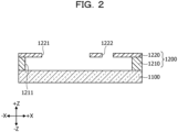
- FIG. 2 is a cross-sectional view illustrating the vapor deposition mask used in the first reference example.
- FIG. 2 corresponds to a cross-sectional view taken along a line II-II in FIG. 1 .
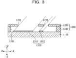
- FIGs. 3 and 4 are cross-sectional views illustrating a method for manufacturing a Josephson device according to the first reference example.
- FIGs. 5 and 6 are schematic views illustrating a relationship between a substrate and a vapor deposition source at the time of vapor deposition in the first reference example.
- a vapor deposition mask 1200 used in the first reference example includes a first resist layer 1210 and a second resist layer 1220.
- the first resist layer 1210 is provided on a substrate 1100
- the second resist layer 1220 is provided on the first resist layer 1210.
- the second resist layer 1220 includes a first opening pattern 1221 extending in an X-axis direction parallel to an upper surface of the substrate 1100 and a second opening pattern 1222 extending in a Y-axis direction parallel to the upper surface of the substrate 1100 and perpendicular to the X-axis direction.
- the second opening pattern 1222 is positioned in the vicinity of one end of the first opening pattern 1221.
- the first resist layer 1210 includes an opening pattern 1211 surrounding the first opening pattern 1221 and the second opening pattern 1222 at least in a plan view from a Z-axis direction perpendicular to the upper surface of the substrate 1100.
- a first superconducting metal layer 1310 is formed on the substrate 1100 by a vapor deposition method.
- the Z-axis direction of the substrate 1100 is not parallel to a traveling direction 1501 of an evaporation substance emitted from a vapor deposition source 1500.
- a direction inclined from a +Z side to a +X side of the substrate 1100 is a direction parallel to the traveling direction 1501.
- An inclination angle ⁇ 1 at this time is such an extent that the evaporation substance passes through both the first opening pattern 1221 and the second opening pattern 1222.
- the first superconducting metal layer 1310 is formed at a position shifted to a -X side from the first opening pattern 1221 and the second opening pattern 1222 in a plan view from the Z-axis direction.
- the first superconducting metal layer 1310 includes a first pattern 1311 including an evaporation raw material that has passed through the first opening pattern 1221, and a second pattern 1312 including an evaporation raw material that has passed through the second opening pattern 1222.
- the first pattern 1311 extends in the X-axis direction similarly to the first opening pattern 1221, and the second pattern 1312 extends in the Y-axis direction similarly to the second opening pattern 1222.
- the Z-axis direction of the substrate 1100 is not parallel to the traveling direction 1501 of the evaporation substance emitted from the vapor deposition source 1500.
- a direction inclined from the +Z side to the -X side of the substrate 1100 is a direction parallel to the traveling direction 1501.
- An inclination angle ⁇ 2 at this time is such an extent that the evaporation substance passes through both the first opening pattern 1221 and the second opening pattern 1222.
- the second superconducting metal layer 1320 is formed at a position shifted to the +X side from the first opening pattern 1221 and the second opening pattern 1222 in a plan view from the Z-axis direction.
- the second superconducting metal layer 1320 includes a first pattern 1321 including an evaporation raw material that has passed through the first opening pattern 1221, and a second pattern 1322 including an evaporation raw material that has passed through the second opening pattern 1222.
- the first pattern 1321 extends in the X-axis direction similarly to the first opening pattern 1221
- the second pattern 1322 extends in the Y-axis direction similarly to the second opening pattern 1222.
- the second pattern 1312 of the first superconducting metal layer 1310 and the first pattern 1321 of the second superconducting metal layer 1320 are stacked with the oxide film 1330 interposed therebetween.
- the second pattern 1312 of the first superconducting metal layer 1310, the oxide film 1330, and the first pattern 1321 of the second superconducting metal layer 1320 constitute a Josephson device.
- an incident angle of the evaporation substance to the substrate 1100 when the first superconducting metal layer 1310 is formed varies depending on a position in the X-axis direction.
- an incident angle to a center of the substrate 1100 is 90° - ⁇ 1
- an incident angle to the vicinity of an end on the +X side of the substrate 1100 is greater than 90° - ⁇ 1 and the incident angle to the vicinity of the end on the +X side of the substrate 1100 is smaller than 90° - ⁇ 1.
- a diameter of the substrate 1100 is 6 inches (about 15 cm)
- a distance between the center of the substrate 1100 and the vapor deposition source 1500 is 60 cm
- the inclination angle ⁇ 1 is 30°
- the incident angle to the center of the substrate 1100 is 60°
- the incident angle to the end on the +X side of the substrate 1100 is 66.3°
- the incident angle to the vicinity of the end on the +X side of the substrate 1100 is 54.2°. Therefore, a difference of up to 12.1° occurs in the incident angle.
- an incident angle of the evaporation substance to the substrate 1100 when the second superconducting metal layer 1320 is formed also varies depending on the position in the X-axis direction. For example, when the second superconducting metal layer 1320 is formed, an incident angle to the center of the substrate 1100 is 90° - ⁇ 2, but an incident angle to the vicinity of the end on the +X side of the substrate 1100 is smaller than 90° - ⁇ 2 and the incident angle to the vicinity of the end on the +X side of the substrate 1100 is greater than 90° - ⁇ 2.
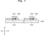
- FIG. 7 is a cross-sectional view illustrating the difference in shape between the two Josephson devices in the first reference example.
- FIG. 8 is a plan view illustrating a vapor deposition mask used in the second reference example.
- FIGs. 9 and 10 are cross-sectional views illustrating the vapor deposition mask used in the second reference example.
- FIG. 9 corresponds to a cross-sectional view taken along a line IX-IX in FIG. 8
- FIG. 10 corresponds to a cross-sectional view taken along a line X-X in FIG. 8 .
- FIGs. 11 and 12 are cross-sectional views illustrating a method for manufacturing a Josephson device according to the second reference example.
- FIGs. 11 and 12 correspond to cross-sectional views taken along a line XI-XI in FIG. 8 .
- a vapor deposition mask 2200 used in the second reference example includes a first resist layer 2210 and a second resist layer 2220.
- the first resist layer 2210 is provided on a substrate 1100
- the second resist layer 2220 is provided on the first resist layer 2210.
- the second resist layer 2220 includes a first opening pattern 2221 extending in the X-axis direction parallel to an upper surface of the substrate 1100 and a second opening pattern 2222 extending in the Y-axis direction parallel to the upper surface of the substrate 1100 and perpendicular to the X-axis direction.
- the first opening pattern 2221 and the second opening pattern 2222 intersect each other in the vicinity of a center in a longitudinal direction.
- the first resist layer 2210 includes a first opening pattern 2211 surrounding the first opening pattern 2221 and a second opening pattern 2212 surrounding the second opening pattern 2222 in a plan view from the Z-axis direction perpendicular to the upper surface of the substrate 1100.
- a first superconducting metal layer 2310 is formed on the substrate 1100 by the vapor deposition method.
- the Z-axis direction of the substrate 1100 is not parallel to a traveling direction 1501 of an evaporation substance emitted from a vapor deposition source 1500.
- a direction inclined from the +Z side to the +X side of the substrate 1100 is a direction parallel to the traveling direction 1501.
- An inclination angle at this time is such an extent that the evaporation substance passes through the first opening pattern 2221 but may not pass through the second opening pattern 2222.
- the first superconducting metal layer 2310 extends in the X-axis direction similarly to the first opening pattern 2221.
- a surface of the first superconducting metal layer 2310 is oxidized to form an oxide film 2330.
- a second superconducting metal layer 2320 is formed on the substrate 1100 and the oxide film 2330 by the vapor deposition method.
- the Z-axis direction of the substrate 1100 is not parallel to the traveling direction 1501 of the evaporation substance emitted from the vapor deposition source 1500.
- a direction inclined from the +Z side to a +Y side of the substrate 1100 is a direction parallel to the traveling direction 1501.
- An inclination angle at this time is such an extent that the evaporation substance passes through the second opening pattern 2222 but may not pass through the first opening pattern 2221.
- the second superconducting metal layer 2320 extends in the Y-axis direction similarly to the second opening pattern 2222. That is, the first superconducting metal layer 2310 and the second superconducting metal layer 2320 intersect.
- the first superconducting metal layer 2310 and the second superconducting metal layer 2320 are stacked with the oxide film 2330 interposed therebetween.
- the first superconducting metal layer 2310, the oxide film 2330, and the second superconducting metal layer 2320 constitute a Josephson device.
- an incident angle of the evaporation substance to the substrate 1100 when the first superconducting metal layer 2310 is formed varies depending on a position in the X-axis direction
- an incident angle of the evaporation substance to the substrate 1100 when the second superconducting metal layer 2320 is formed varies depending on a position in the Y-axis direction.
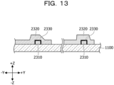
- FIG. 13 is a cross-sectional view illustrating the difference in shape between the two Josephson devices in the second reference example.
- the inventor of the present application conducted intensive studies to suppress variations in characteristics among a plurality of qubits, and conceived the following embodiments.
- FIG. 14 is a plan view illustrating a Josephson device according to the first embodiment.
- FIG. 15 is a cross-sectional view illustrating the Josephson device according to the first embodiment.
- FIG. 15 corresponds to a cross-sectional view taken along a dash-dot line in FIG. 14 .
- a Josephson device 1 includes a first superconducting metal layer 110, a second superconducting metal layer 120, and an insulating layer 130.
- the first superconducting metal layer 110 includes an upper surface 111
- the second superconducting metal layer 120 includes a lower surface 122.
- the lower surface 122 faces the upper surface 111.
- Each of the first superconducting metal layer 110 and the second superconducting metal layer 120 has a substantially cylindrical shape.
- the insulating layer 130 is provided between the upper surface 111 of the first superconducting metal layer 110 and the lower surface 122 of the second superconducting metal layer 120.
- an outline of the lower surface 122 is inside an outline of the upper surface 111.
- the insulating layer 130 may also be provided on a side surface of the first superconducting metal layer 110.
- the Josephson device 1 is provided on, for example, a substrate 100.
- the upper surface 111 is an example of a first surface
- the lower surface 122 is an example of a second surface.
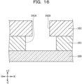
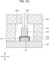
- FIGs. 16 and 20 are cross-sectional views illustrating the method for manufacturing the Josephson device 1 according to the first embodiment.
- FIG. 21 is a schematic view illustrating a relationship between the substrate and a vapor deposition source at the time of vapor deposition in the first embodiment.
- a resist layer 191 including an opening 191X and a resist layer 192 including an opening 192X are formed on the substrate 100.
- the resist layer 191 is formed on a side of the substrate 100 of the resist layer 192.
- the opening 192X has a shape and a size corresponding to the upper surface of the first superconducting metal layer 110 to be formed in a plan view.
- the opening 191X surrounds the opening 192X in a plan view.
- the first superconducting metal layer 110 is formed on the substrate 100 inside the opening 191X by the vapor deposition method using the resist layers 191 and 192 as vapor deposition masks.
- the Z-axis direction of the substrate 100 is parallel to a traveling direction 151 of an evaporation substance (first evaporation substance) emitted from a vapor deposition source 150. Therefore, an incident angle of the evaporation substance to a center of the substrate 100 is 90°.
- the resist layers 191 and 192 are removed.
- the evaporation substance is deposited also on the resist layer 192, but the deposited evaporation substance is removed together with the resist layers 191 and 192. That is, lift-off is performed.
- the surface (the upper surface and the side surface) of the first superconducting metal layer 110 is oxidized to form the insulating layer 130.
- a resist layer 193 including an opening 193X and a resist layer 194 including an opening 194X are formed on the substrate 100.
- the resist layer 193 is formed on a side of the substrate 100 of the resist layer 194.
- the opening 194X surrounds the outline of the upper surface 111 of the first superconducting metal layer 110 in a plan view, and has a shape and a size corresponding to an upper surface of the second superconducting metal layer 120 to be formed.
- the opening 193X surrounds the opening 194X in a plan view.
- the second superconducting metal layer 120 is formed on a portion of the insulating layer 130 on the upper surface 111 of the first superconducting metal layer 110 inside the opening 193X by the vapor deposition method using the resist layers 193 and 194 as vapor deposition masks. Also at this time, as illustrated in FIG. 21 , the Z-axis direction of the substrate 100 is parallel to the traveling direction 151 of the evaporation substance (second evaporation substance). Therefore, an incident angle of the evaporation substance to the center of the substrate 100 is 90°.
- the resist layers 193 and 194 are removed (see FIG. 15 ).
- the evaporation substance is deposited also on the resist layer 194, but the deposited evaporation substance is removed together with the resist layers 193 and 194. That is, lift-off is performed.
- the Josephson device 1 according to the first embodiment may be manufactured.
- the outline of the lower surface 122 of the second superconducting metal layer 120 is inside the outline of the upper surface 111 of the first superconducting metal layer 110 in a plan view. Therefore, the Z-axis direction of the substrate 100 may be made parallel to the traveling direction 151 of the evaporation substance at the time of the formation of the first superconducting metal layer 110 and at the time of the formation of the second superconducting metal layer 120. Therefore, it is possible to suppress a difference in incident angle of the evaporation substance to the substrate 100.
- an incident angle to the center of the substrate 100 is 90° and an incident angle to an end of the substrate 100 is 82.9°. Therefore, the difference in incident angle is at most 7.1°.
- FIG. 22 is a plan view illustrating a Josephson device according to a second embodiment.
- FIG. 23 is a cross-sectional view illustrating the Josephson device according to the second embodiment.
- FIG. 23 corresponds to a cross-sectional view taken along a dash-dot line XXIII-XXIII.
- a Josephson device 2 includes a first superconducting metal layer 210, a second superconducting metal layer 220, and an insulating layer 230.
- the first superconducting metal layer 210 includes an upper surface 211
- the second superconducting metal layer 220 includes a lower surface 222.
- the lower surface 222 faces the upper surface 211.
- the first superconducting metal layer 210 has a substantially truncated cone shape
- the second superconducting metal layer 220 has a substantially cylindrical shape.
- the insulating layer 230 is provided between the upper surface 211 of the first superconducting metal layer 210 and the lower surface 222 of the second superconducting metal layer 220.
- an outline of the lower surface 222 is inside an outline of the upper surface 211.
- the insulating layer 230 may also be provided on a side surface of the first superconducting metal layer 210.
- the Josephson device 2 is provided on, for example, a substrate 100.
- the upper surface 211 is an example of the first surface
- the lower surface 222 is an example of the second surface.
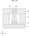
- FIGs. 24 and 27 are cross-sectional views illustrating the method for manufacturing the Josephson device 2 according to the second embodiment.
- FIG. 28 is a schematic view illustrating a relationship between the substrate and a vapor deposition source at the time of vapor deposition in the second embodiment.
- a resist layer 291 including an opening 291X and a resist layer 292 including an opening 292X are formed on the substrate 100.
- the resist layer 291 is formed on a side of the substrate 100 of the resist layer 292.
- the opening 292X has a shape and a size corresponding to an upper surface of the second superconducting metal layer 220 to be formed in a plan view.
- the opening 291X has a shape and a size surrounding an outline of a lower surface of the first superconducting metal layer 210 to be formed in a plan view.
- the first superconducting metal layer 210 is formed on the substrate 100 inside the opening 291X by the vapor deposition method using the resist layers 291 and 292 as vapor deposition masks.
- the Z-axis direction of the substrate 100 is not parallel to a traveling direction 151 of an evaporation substance (first evaporation substance) emitted from a vapor deposition source 150, and the substrate 100 is rotated around a straight line passing through a center of an upper surface of the substrate 100 and perpendicular to the upper surface as a rotation center.
- An inclination angle ⁇ 3 at this time is such an extent that a portion where the lower surface 222 of the second superconducting metal layer 220 to be formed later is positioned may be seen from the vapor deposition source 150 at any position in the substrate 100.
- the inclination angle ⁇ 3 is, for example, about 1° to 10°.
- the surface (the upper surface and side surfaces) of the first superconducting metal layer 210 is oxidized to form the insulating layer 230 while leaving the resist layers 291 and 292.
- the second superconducting metal layer 220 is formed on a portion of the insulating layer 230 on the upper surface 211 of the first superconducting metal layer 210 inside the opening 291X by the vapor deposition method using the resist layers 291 and 292 as vapor deposition masks.
- the Z-axis direction of the substrate 100 is parallel to the traveling direction 151 of the evaporation substance (second evaporation substance). Therefore, an incident angle of the evaporation substance to the center of the substrate 100 is 90°.
- the formation of the first superconducting metal layer 210, the formation of the insulating layer 230, and the formation of the second superconducting metal layer 220 are continuously performed while maintaining a vacuum state in a vacuum chamber.
- the resist layers 291 and 292 are removed (see FIG. 23 ).
- the evaporation substance is deposited also on the resist layer 292, but the deposited evaporation substance is removed together with the resist layers 291 and 292. That is, lift-off is performed.
- the Josephson device 2 according to the second embodiment may be manufactured.
- the outline of the lower surface 222 of the second superconducting metal layer 220 is inside the outline of the upper surface 211 of the first superconducting metal layer 210 in a plan view. Therefore, the inclination angle ⁇ 3 at the time of the formation of the first superconducting metal layer 210 may be reduced, and the Z-axis direction of the substrate 100 may be made parallel to the traveling direction 151 of the evaporation substance at the time of the formation of the second superconducting metal layer 220. Therefore, similarly to the first embodiment, it is possible to suppress a difference in incident angle of the evaporation substance to the substrate 100.
- first superconducting metal layer 210 and the second superconducting metal layer 220 may be formed using the resist layers 191 and 192, a throughput may be improved.
- a third embodiment relates to a superconducting circuit including a Josephson device.
- FIG. 29 is a plan view illustrating the superconducting circuit according to the third embodiment.
- FIG. 30 is a cross-sectional view illustrating the superconducting circuit according to the third embodiment.
- FIG. 29 illustrates some components such as an insulating layer in a transparent manner.
- FIG. 30 corresponds to a cross-sectional view taken along a line XXX-XXX in FIG. 29 .
- a superconducting circuit 30 mainly includes a substrate 300, a first superconducting metal layer 310, a second superconducting metal layer 320, an insulating layer 330, a third superconducting metal layer 340, a fourth superconducting metal layer 350, and a dielectric layer 390.
- the substrate 300 is, for example, a high-resistance Si substrate.
- the third superconducting metal layer 340 is formed on the substrate 300.
- the third superconducting metal layer 340 extends in the X-axis direction parallel to an upper surface of the substrate 300.
- One end of the third superconducting metal layer 340 has a semicircular arc shape in a plan view.
- the third superconducting metal layer 340 is, for example, an Al layer having a thickness of 30 nm to 70 nm.
- the first superconducting metal layer 310 is formed on the third superconducting metal layer 340.
- the first superconducting metal layer 310 has a substantially truncated cone shape.
- the first superconducting metal layer 310 is, for example, an Al layer having a thickness of 30 nm to 70 nm.
- An insulating layer 341 is formed on a surface (an upper surface and a side surface) of the third superconducting metal layer 340 except for a portion where the first superconducting metal layer 310 is formed.
- the insulating layer 341 is, for example, an Al oxide layer having a thickness of 1 nm to 5 nm.
- the insulating layer 330 is formed on a surface (an upper surface and a side surface) of the first superconducting metal layer 310.
- the insulating layer 330 is, for example, an Al oxide layer having a thickness of 1 nm to 5 nm.
- the second superconducting metal layer 320 is formed on a portion of the insulating layer 330 on an upper surface 311 of the first superconducting metal layer 310.
- a lower surface 322 of the second superconducting metal layer 320 faces the upper surface 311 of the first superconducting metal layer 310, and a part of the insulating layer 330 is provided between the upper surface 311 of the first superconducting metal layer 310 and the lower surface 322 of the second superconducting metal layer 320.
- an outline of the lower surface 322 is inside an outline of the upper surface 311.
- the second superconducting metal layer 320 has a substantially cylindrical shape.
- the second superconducting metal layer 320 is, for example, an Al layer having a thickness of 250 nm to 350 nm.
- the upper surface 311 is an example of the first surface
- the lower surface 322 is an example of the second surface.
- a dielectric layer 390 covering the third superconducting metal layer 340, the insulating layer 341, the first superconducting metal layer 310, and the insulating layer 330 is formed on the substrate 300.
- An upper surface of the dielectric layer 390 is positioned above the lower surface 322 of the second superconducting metal layer 320 and below an upper surface of the second superconducting metal layer 320 in the Z-axis direction perpendicular to the upper surface of the substrate 300.
- the dielectric layer 390 is, for example, a benzocyclobutene (BCB) layer.
- An insulating layer 321 is formed on a portion of a side surface of the second superconducting metal layer 320 below the upper surface of the dielectric layer 390. That is, the insulating layer 321 is formed between the second superconducting metal layer 320 and the dielectric layer 390.
- the insulating layer 321 is, for example, an Al oxide layer having a thickness of 1 nm to 5 nm.
- the fourth superconducting metal layer 350 is formed on the dielectric layer 390.
- the fourth superconducting metal layer 350 is in contact with a portion of the second superconducting metal layer 320 above the upper surface of the dielectric layer 390.
- the fourth superconducting metal layer 350 extends in the X-axis direction.
- the fourth superconducting metal layer 350 is, for example, an Al layer having a thickness of 30 nm to 70 nm.
- An insulating layer 351 is formed on a surface (an upper surface and a side surface) of the fourth superconducting metal layer 350.
- the insulating layer 351 is, for example, an Al oxide layer having a thickness of 1 nm to 5 nm.
- the superconducting circuit 30 includes a Josephson device 3 including the first superconducting metal layer 310, the second superconducting metal layer 320, and the insulating layer 330.
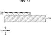
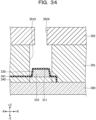
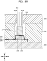
- FIGs. 31 to 38 are cross-sectional views illustrating the method for manufacturing the superconducting circuit 30 according to the third embodiment.
- the third superconducting metal layer 340 is formed on the substrate 300.
- the third superconducting metal layer 340 may be formed by, for example, vapor deposition and lift-off similarly to the formation of the first superconducting metal layer 110 in the first embodiment, and the like. Film formation of the third superconducting metal layer 340 is performed in vacuum, and when the third superconducting metal layer 340 is exposed to the atmosphere, the insulating layer 341 is formed on the surface of the third superconducting metal layer 340 by natural oxidation.
- a resist layer 391 including an opening 391X and a resist layer 392 including an opening 392X are formed on the substrate 300 so as to cover the third superconducting metal layer 340 and the insulating layer 341.
- the resist layer 391 including the opening 391X and the resist layer 392 including the opening 392X may be formed by performing electron beam exposure after forming the two resist layers.
- the opening 392X has a shape and a size corresponding to the upper surface of the second superconducting metal layer 320 to be formed in a plan view.
- the opening 391X has a shape and a size surrounding an outline of a lower surface of the first superconducting metal layer 310 to be formed in a plan view. A part of the insulating layer 341 is exposed from the openings 391X and 392X.
- the portion of the insulating layer 341 exposed from the openings 391X and 392X is removed by ion milling using Ar ions in vacuum.
- the first superconducting metal layer 310 is formed on a portion of the third superconducting metal layer 340 from which the insulating layer 341 is removed by the vapor deposition method using the resist layers 391 and 392 as vapor deposition masks.
- the Z-axis direction of the substrate 300 is not parallel to a traveling direction of an evaporation substance (first evaporation substance) emitted from a vapor deposition source, and the substrate 300 is rotated around a straight line passing through a center of the upper surface of the substrate 300 and perpendicular to the upper surface as a rotation center.
- An inclination angle at this time is such an extent that a portion where the lower surface 322 of the second superconducting metal layer 320 to be formed later is positioned may be seen from the vapor deposition source at any position in the substrate 300.
- the inclination angle is, for example, about 1° to 10°.
- the surface (the upper surface and the side surface) of the first superconducting metal layer 310 is oxidized to form the insulating layer 330 while leaving the resist layers 391 and 392.
- oxygen is supplied into vacuum without exposure to the atmosphere.
- the second superconducting metal layer 320 is formed on a portion of the insulating layer 330 on the upper surface 311 of the first superconducting metal layer 310 inside the opening 391X by the vapor deposition method using the resist layers 391 and 392 as vapor deposition masks.
- the Z-axis direction of the substrate 300 is parallel to the traveling direction of the evaporation substance (second evaporation substance).
- the ion milling of the insulating layer 341, the formation of the first superconducting metal layer 310, the formation of the insulating layer 330, and the formation of the second superconducting metal layer 320 are continuously performed while maintaining a vacuum state in a vacuum chamber.
- the resist layers 391 and 392 are removed.
- the evaporation substance is deposited also on the resist layer 392, but the deposited evaporation substance is removed together with the resist layers 391 and 392. That is, lift-off is performed.
- the insulating layer 321 is formed on the surface of the second superconducting metal layer 320 by natural oxidation.
- the dielectric layer 390 covering the third superconducting metal layer 340, the insulating layer 341, the first superconducting metal layer 310, the insulating layer 330, the second superconducting metal layer 320, and the insulating layer 321 is formed on the substrate 300.
- the upper surface of the dielectric layer 390 is positioned above the upper surface of the second superconducting metal layer 320 in the Z-axis direction.
- spin coating of a BCB resin is performed, and then the BCB resin is thermally cured.
- the dielectric layer 390 is etched back by dry etching, and the upper surface of the dielectric layer 390 is positioned below the upper surface of the second superconducting metal layer 320. That is, a part of the second superconducting metal layer 320 protrudes from the dielectric layer 390.
- the insulating layer 321 formed on a surface of the portion of the second superconducting metal layer 320 protruding from the dielectric layer 390 is removed, and the fourth superconducting metal layer 350 in contact with the portion of the second superconducting metal layer 320 above the upper surface of the dielectric layer 390 is formed on the dielectric layer 390 (see FIG. 30 ).
- the insulating layer 321 may be removed by ion milling using Ar ions.
- the fourth superconducting metal layer 350 may be formed by, for example, vapor deposition and lift-off similarly to the formation of the third superconducting metal layer 340, and the like. When the fourth superconducting metal layer 350 is exposed to the atmosphere, the insulating layer 351 is formed on the surface of the fourth superconducting metal layer 350 by natural oxidation.
- the superconducting circuit 30 according to the third embodiment may be manufactured.
- the outline of the lower surface 322 of the second superconducting metal layer 320 is inside the outline of the upper surface 311 of the first superconducting metal layer 310 in a plan view. Therefore, the inclination angle at the time of the formation of the first superconducting metal layer 310 may be reduced, and the Z-axis direction of the substrate 300 may be made parallel to the traveling direction of the evaporation substance at the time of the formation of the second superconducting metal layer 320. Therefore, similarly to the first embodiment, it is possible to suppress a difference in incident angle of the evaporation substance to the substrate 300.
- the third superconducting metal layer 340 in contact with the first superconducting metal layer 310 and the fourth superconducting metal layer 350 in contact with the second superconducting metal layer 320 may be used as wirings coupled to the Josephson device 3.
- FIG. 39 is a plan view illustrating the superconducting circuit according to the fourth embodiment.
- FIG. 40 is a cross-sectional view illustrating the superconducting circuit according to the fourth embodiment.
- FIG. 39 illustrates some components such as an insulating layer in a transparent manner.
- FIG. 40 corresponds to a cross-sectional view taken along a line XL-XL in FIG. 39 .
- a superconducting circuit 40 according to the fourth embodiment mainly includes a substrate 300, a first superconducting metal layer 310, a second superconducting metal layer 320, an insulating layer 330, a third superconducting metal layer 340, a fourth superconducting metal layer 450, a fifth superconducting metal layer 460, and a dielectric layer 390.
- the fifth superconducting metal layer 460 is formed on the substrate 300. Similarly to the third superconducting metal layer 340, the fifth superconducting metal layer 460 extends in the X-axis direction parallel to an upper surface of the substrate 300. The fifth superconducting metal layer 460 is disposed on the +X side of the third superconducting metal layer 340 away from the third superconducting metal layer 340. The fifth superconducting metal layer 460 is, for example, an Al layer having a thickness of 30 nm to 70 nm. An insulating layer 461 is formed on a surface (an upper surface and a side surface) of the fifth superconducting metal layer 460.
- the insulating layer 461 is, for example, an Al oxide layer having a thickness of 1 nm to 5 nm.
- An opening 461X overlapping a part of the fifth superconducting metal layer 460 in a plan view is formed in the insulating layer 461.
- the dielectric layer 390 also covers the fifth superconducting metal layer 460 and the insulating layer 461.
- An opening 490X overlapping the opening 461X in a plan view is formed in the dielectric layer 390.
- the fourth superconducting metal layer 450 is formed on the dielectric layer 390 and inside the openings 490X and 461X.
- the fourth superconducting metal layer 450 is in contact with a portion of the second superconducting metal layer 320 above an upper surface of the dielectric layer 390 and the fifth superconducting metal layer 460.
- the fourth superconducting metal layer 450 is, for example, an Al layer.
- a thickness of a portion on the dielectric layer 390 of the fourth superconducting metal layer 450 is, for example, 30 nm to 70 nm.
- An insulating layer 451 is formed on a surface (an upper surface and a side surface) of the fourth superconducting metal layer 450.
- the insulating layer 451 is, for example, an Al oxide layer having a thickness of 1 nm to 5 nm.
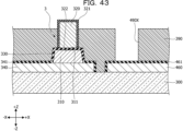
- FIGs. 41 to 43 are cross-sectional views illustrating the method for manufacturing the superconducting circuit 40 according to the fourth embodiment.
- the third superconducting metal layer 340 and the fifth superconducting metal layer 460 are formed on the substrate 300.
- the third superconducting metal layer 340 and the fifth superconducting metal layer 460 may be formed by, for example, vapor deposition and lift-off similarly to the formation of the first superconducting metal layer 110 in the first embodiment, and the like.
- Film formation of the third superconducting metal layer 340 and the fifth superconducting metal layer 460 is performed in vacuum, and when the third superconducting metal layer 340 and the fifth superconducting metal layer 460 are exposed to the atmosphere, an insulating layer 341 is formed on a surface of the third superconducting metal layer 340 and the insulating layer 461 is formed on the surface of the fifth superconducting metal layer 460 by natural oxidation.
- a resist layer 491 including an opening 491X is formed on the dielectric layer 390.
- the opening 491X has a shape and a size corresponding to the opening 490X in Fig. 40 to be formed in a plan view.
- the resist layer 491 and the dielectric layer 390 are etched back by dry etching, and the opening 490X is formed in the dielectric layer 390 while the upper surface of the dielectric layer 390 is positioned below an upper surface of the second superconducting metal layer 320.
- the resist layer 491 is removed by etching back.
- the insulating layer 321 formed on a surface of a portion of the second superconducting metal layer 320 protruding from the dielectric layer 390 and the insulating layer 461 exposed from the opening 490X are removed.
- the opening 461X is formed in the insulating layer 461.
- the fourth superconducting metal layer 450 in contact with the portion of the second superconducting metal layer 320 above the upper surface of the dielectric layer 390 and the fifth superconducting metal layer 460 is formed (see FIG. 40 ).
- the insulating layers 321 and 461 may be removed by ion milling using Ar ions.
- the fourth superconducting metal layer 450 may be formed by, for example, vapor deposition and lift-off similarly to the formation of the third superconducting metal layer 340 and the fifth superconducting metal layer 460, and the like.
- the insulating layer 451 is formed on the surface of the fourth superconducting metal layer 450 by natural oxidation.
- the superconducting circuit 40 according to the fourth embodiment may be manufactured.
- a difference in shape among a plurality of Josephson devices 3 formed on the substrate 300 is slight, and it is possible to suppress variations in characteristics of the Josephson devices 3.
- the third superconducting metal layer 340 in contact with the first superconducting metal layer 310, the fourth superconducting metal layer 450 in contact with the second superconducting metal layer 320, and the fifth superconducting metal layer 460 in contact with the fourth superconducting metal layer 450 may be used as wirings coupled to the Josephson device 3.
- FIG. 44 is a cross-sectional view illustrating the superconducting circuit according to the fifth embodiment. Similarly to FIG. 40 , FIG. 44 corresponds to a cross-sectional view taken along the line XL-XL in FIG. 39 .
- a superconducting circuit 50 mainly includes a substrate 300, a first superconducting metal layer 310, a second superconducting metal layer 320, an insulating layer 330, a third superconducting metal layer 340, a fourth superconducting metal layer 450, and a fifth superconducting metal layer 460.
- a dielectric layer 390 is not provided in the superconducting circuit 50.
- An insulating layer 451 is formed on substantially an entire side surface of the fourth superconducting metal layer 450 so as to be coupled to an insulating layer 461.
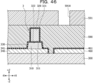
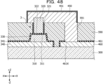
- FIGs. 45 to 48 are cross-sectional views illustrating the method for manufacturing the superconducting circuit 50 according to the fifth embodiment.
- resist layers 391 and 392 are removed similarly to the fourth embodiment.
- a sacrificial layer 590 covering the third superconducting metal layer 340, an insulating layer 341, the first superconducting metal layer 310, the insulating layer 330, the second superconducting metal layer 320, and an insulating layer 321 is formed on the substrate 300.
- An upper surface of the sacrificial layer 590 is positioned above an upper surface of the second superconducting metal layer 320 in the Z-axis direction.
- spin coating of a polymethylglutarimide (PMGI) resin is performed, and then the PMGI resin is thermally cured.
- a resist layer 591 including an opening 591X is formed on the sacrificial layer 590.
- the opening 591X has a shape and a size corresponding to a portion extending in the Z-axis direction of the fourth superconducting metal layer 450 to be formed later in a plan view.
- the resist layer 591 and the sacrificial layer 590 are etched back by dry etching, and an opening 590X is formed in the sacrificial layer 590 while the upper surface of the sacrificial layer 590 is positioned below the upper surface of the second superconducting metal layer 320.
- the resist layer 591 is removed by etching back.
- the insulating layer 321 formed on a surface of a portion of the second superconducting metal layer 320 protruding from the sacrificial layer 590 and the insulating layer 461 exposed from the opening 590X are removed.
- the opening 461X is formed in the insulating layer 461.
- the fourth superconducting metal layer 450 in contact with the portion of the second superconducting metal layer 320 above the upper surface of the sacrificial layer 590 and the fifth superconducting metal layer 460 is formed.
- the insulating layer 451 is formed on a surface of the fourth superconducting metal layer 450 by natural oxidation.
- the sacrificial layer 590 is dissolved and removed using a solvent (see FIG. 44 ).
- the superconducting circuit 50 according to the fifth embodiment may be manufactured.
- a difference in shape among a plurality of Josephson devices 3 formed on the substrate 300 is slight, and it is possible to suppress variations in characteristics of the Josephson devices 3.
- a dielectric includes a defect called a two-level system (TLS)
- TLS two-level system
- the superconducting circuit 50 has an air bridge structure, and the dielectric layer 390 is not provided around the Josephson device 3. Therefore, according to the present embodiment, a coherence time of the Josephson device 3 may be extended, and the present embodiment is suitable for a quantum operation.
- FIG. 49 is a plan view illustrating the superconducting circuit according to the sixth embodiment.
- FIG. 50 is a cross-sectional view illustrating the superconducting circuit according to the sixth embodiment.
- FIG. 50 corresponds to a cross-sectional view taken along a line L-L in FIG. 49 .
- a trench 601 is formed on a surface of a substrate 300 along edges of a third superconducting metal layer 340 and an insulating layer 341 around a Josephson device 3.
- the trench 601 is formed along the edge of the insulating layer 341 formed on an end of the third superconducting metal layer 340 having a semicircular arc shape in a plan view and a side surface of the end.
- a depth of the trench 601 is, for example, 50 nm to 200 nm.
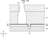
- FIGs. 51 to 53 are cross-sectional views illustrating the method for manufacturing the superconducting circuit 60 according to the sixth embodiment.
- the third superconducting metal layer 340 and a fifth superconducting metal layer 460 are formed on the substrate 300.
- the insulating layer 341 is formed on a surface of the third superconducting metal layer 340 and an insulating layer 461 is formed on a surface of the fifth superconducting metal layer 460 by natural oxidation.
- a resist layer 691 including an opening 691X is formed on the substrate 300 so as to cover the third superconducting metal layer 340, the insulating layer 341, the fifth superconducting metal layer 460, and the insulating layer 461.
- the opening 691X has a shape and a size corresponding to the trench 601 to be formed in a plan view.
- the trench 601 is formed on the surface of the substrate 300 by dry etching using the resist layer 691 as an etching mask.
- the resist layer 691 is removed, and a resist layer 391 including an opening 391X and a resist layer 392 including an opening 392X are formed on the substrate 300, similarly to the fifth embodiment. At this time, the resist layer 391 is also formed inside the trench 601.
- processing from removal of the insulating layer 341 to removal of a sacrificial layer 590 is performed similarly to the fifth embodiment (see FIG. 50 ).
- the superconducting circuit 60 according to the sixth embodiment may be manufactured.
- a difference in shape among a plurality of the Josephson devices 3 formed on the substrate 300 is slight, and it is possible to suppress variations in characteristics of the Josephson devices 3.
- a distance from the TLS existing on the surface of the substrate 300 of the Josephson device 3 may be increased to reduce a dielectric loss. Therefore, a coherence time of the Josephson device 3 may be further extended.
- FIG. 54 is a cross-sectional view illustrating the superconducting circuit according to the seventh embodiment. Similarly to FIG. 50 , FIG. 54 corresponds to a cross-sectional view taken along the line L-L in FIG. 49 .
- a trench 601 is formed on a surface of a substrate 300 along edges of a third superconducting metal layer 340 and an insulating layer 341 around a Josephson device 3. Moreover, a recess 701 coupled to the trench 601 is formed on the surface of the substrate 300 below the Josephson device 3. Therefore, a space exists between the third superconducting metal layer 340 and the substrate 300. Furthermore, the insulating layer 341 is formed also on a lower surface (a surface on a -Z side) of the third superconducting metal layer 340. A depth of the trench 601 and the recess 701 is, for example, 50 nm to 200 nm.
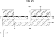
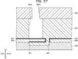
- FIGs. 55 to 57 are cross-sectional views illustrating the method for manufacturing the superconducting circuit 70 according to the seventh embodiment.
- the third superconducting metal layer 340 and a fifth superconducting metal layer 460 are formed on the substrate 300.
- the insulating layer 341 is formed on a surface of the third superconducting metal layer 340 and an insulating layer 461 is formed on a surface of the fifth superconducting metal layer 460 by natural oxidation.
- a resist layer 791 including an opening 791X is formed on the substrate 300 so as to cover the third superconducting metal layer 340, the insulating layer 341, the fifth superconducting metal layer 460, and the insulating layer 461.
- the opening 791X has a shape and a size corresponding to the trench 601 and the recess 701 to be formed in a plan view.
- the trench 601 and the recess 701 are formed on the surface of the substrate 300 by dry etching using the resist layer 791 as an etching mask. For example, by making a dry etching pressure higher than that at the time of the formation of the trench 601 in the sixth embodiment, side etching of the substrate 300 may be easily caused.
- the resist layer 791 is removed, and a resist layer 391 including an opening 391X and a resist layer 392 including an opening 392X are formed on the substrate 300, similarly to the fifth embodiment.
- the resist layer 391 is also formed inside the trench 601 and the recess 701.
- the insulating layer 341 is formed also on the lower surface of the third superconducting metal layer 340 by natural oxidation.
- processing from removal of the insulating layer 341 to removal of a sacrificial layer 590 is performed similarly to the fifth embodiment (see FIG. 54 ).
- the superconducting circuit 70 according to the seventh embodiment may be manufactured.
- a difference in shape among a plurality of the Josephson devices 3 formed on the substrate 300 is slight, and it is possible to suppress variations in characteristics of the Josephson devices 3.
- a dielectric loss may be further reduced. Therefore, a coherence time of the Josephson device 3 may be still further extended.
- a material of the superconducting metal layer is not particularly limited.
- the material of the superconducting metal layer may be Al, Nb, Nb nitride, Ta, Ta nitride, Ti nitride, or the like. That is, the superconducting metal layer may include Al, Nb, Nb nitride, Ta, Ta nitride, Ti nitride, or the like.
- the third superconducting metal layer 340 and the fifth superconducting metal layer 460 may be Nb layers.
- each superconducting metal layer may have a stacked structure.
- FIG. 58 is a cross-sectional view illustrating a superconducting circuit according to a modification of the fifth embodiment.
- the first superconducting metal layer 310 includes a sixth superconducting metal layer 310A in contact with the third superconducting metal layer 340 and a seventh superconducting metal layer 310B on the sixth superconducting metal layer 310A.
- the sixth superconducting metal layer 310A is an Al layer
- the seventh superconducting metal layer 310B is an Nb layer.
- the third superconducting metal layer 340 and the fifth superconducting metal layer 460 may be Ti nitride layers
- the fourth superconducting metal layer 350 may be a Ta layer.
- FIG. 59 is a diagram illustrating the quantum operation device according to the eighth embodiment.
- a quantum operation device 800 includes a qubit chip 810, a signal generator 820, a signal demodulator 830, and a cryogenic dilution refrigerator 840, as illustrated in FIG. 59 .
- the qubit chip 810 is housed in the cryogenic dilution refrigerator 840, and is cooled to a temperature equal to or lower than 10 mK.
- the signal generator 820 generates a microwave pulse signal, and the microwave pulse signal is input to the qubit chip 810.
- the qubit chip 810 outputs a signal according to the microwave pulse signal, and the signal demodulator 830 demodulates the signal output from the qubit chip 810.
- the signal generator 820 and the signal demodulator 830 are used at, for example, a temperature of about room temperature.
- the qubit chip 810 includes a plurality of superconducting qubits 850, and each superconducting qubit 850 includes a Josephson device 851 and a capacitor 852 electrically coupled in parallel to the Josephson device 851.
- the Josephson device 851 is the Josephson device 3 in any one of the third to seventh embodiments, and a wiring of the third superconducting metal layer and a wiring of the fourth or fifth superconducting metal layer are coupled to the capacitor 852.
- the Josephson device 851 included in the quantum operation device 800 according to the eighth embodiment is the Josephson device 3 in any one of the third to seventh embodiments, variations in characteristics among the plurality of Josephson devices 3 are suppressed, and calculation excellent in reliability may be performed.
Landscapes
- Engineering & Computer Science (AREA)
- General Physics & Mathematics (AREA)
- Theoretical Computer Science (AREA)
- Physics & Mathematics (AREA)
- Manufacturing & Machinery (AREA)
- Mathematical Analysis (AREA)
- Evolutionary Computation (AREA)
- Data Mining & Analysis (AREA)
- Condensed Matter Physics & Semiconductors (AREA)
- Mathematical Optimization (AREA)
- Pure & Applied Mathematics (AREA)
- Computing Systems (AREA)
- General Engineering & Computer Science (AREA)
- Mathematical Physics (AREA)
- Software Systems (AREA)
- Computational Mathematics (AREA)
- Artificial Intelligence (AREA)
- Superconductor Devices And Manufacturing Methods Thereof (AREA)
Abstract
Description
- The present disclosure relates to a Josephson device, a superconducting circuit, a quantum operation device, and a method for manufacturing a Josephson device.
- A quantum operation device includes a plurality of qubits, and the qubits include, for example, a Josephson device. The Josephson device includes two superconducting metal layers and an insulating layer therebetween. Conventionally, various configurations of the Josephson device have been proposed.
-
- Patent Document 1:
U.S. Patent Application Publication No. 2015/0340584 - Patent Document 2:
Japanese Laid-open Patent Publication No. 2-288403 - Patent Document 3:
U.S. Patent Application Publication No. 2004/0183065 - Patent Document 4:
Japanese Laid-open Patent Publication No. 5-315659 - Characteristics may vary among the plurality of qubits included in the quantum operation device. When the characteristics vary among the plurality of qubits, a coherence time varies, and it becomes difficult to perform a stable quantum operation.
- An object of the present disclosure is to provide a Josephson device, a superconducting circuit, a quantum operation device, and a method for manufacturing a Josephson device capable of suppressing variations in characteristics among a plurality of qubits.
- According to an aspect of the present disclosure, there is provided a Josephson device including: a first superconducting metal layer that includes a first surface; a second superconducting metal layer that includes a second surface that faces the first surface; and an insulating layer provided between the first surface and the second surface, in which an outline of the second surface is inside an outline of the first surface in a plan view from a direction perpendicular to the first surface.
- According to the present disclosure, it is possible to suppress variations in characteristics among a plurality of qubits.
-
-
FIG. 1 is a plan view illustrating a vapor deposition mask used in a first reference example. -
FIG. 2 is a cross-sectional view illustrating the vapor deposition mask used in the first reference example. -
FIG. 3 is a cross-sectional view (part 1) illustrating a method for manufacturing a Josephson device according to the first reference example. -
FIG. 4 is a cross-sectional view (part 2) illustrating the method for manufacturing the Josephson device according to the first reference example. -
FIG. 5 is a schematic view (part 1) illustrating a relationship between a substrate and a vapor deposition source at the time of vapor deposition in the first reference example. -
FIG. 6 is a schematic view (part 2) illustrating the relationship between the substrate and the vapor deposition source at the time of vapor deposition in the first reference example. -
FIG. 7 is a cross-sectional view illustrating a difference in shape between two Josephson devices in the first reference example. -
FIG. 8 is a plan view illustrating a vapor deposition mask used in a second reference example. -
FIG. 9 is a cross-sectional view (part 1) illustrating the vapor deposition mask used in the second reference example. -
FIG. 10 is a cross-sectional view (part 2) illustrating the vapor deposition mask used in the second reference example. -
FIG. 11 is a cross-sectional view (part 1) illustrating a method for manufacturing a Josephson device according to the second reference example. -
FIG. 12 is a cross-sectional view (part 2) illustrating the method for manufacturing the Josephson device according to the second reference example. -
FIG. 13 is a cross-sectional view illustrating a difference in shape between two Josephson devices in the second reference example. -
FIG. 14 is a plan view illustrating a Josephson device according to a first embodiment. -
FIG. 15 is a cross-sectional view illustrating the Josephson device according to the first embodiment. -
FIG. 16 is a cross-sectional view (part 1) illustrating a method for manufacturing the Josephson device according to the first embodiment. -
FIG. 17 is a cross-sectional view (part 2) illustrating the method for manufacturing the Josephson device according to the first embodiment. -
FIG. 18 is a cross-sectional view (part 3) illustrating the method for manufacturing the Josephson device according to the first embodiment. -
FIG. 19 is a cross-sectional view (part 4) illustrating the method for manufacturing the Josephson device according to the first embodiment. -
FIG. 20 is a cross-sectional view (part 5) illustrating the method for manufacturing the Josephson device according to the first embodiment. -
FIG. 21 is a schematic view illustrating a relationship between a substrate and a vapor deposition source at the time of vapor deposition in the first embodiment. -
FIG. 22 is a plan view illustrating a Josephson device according to a second embodiment. -
FIG. 23 is a cross-sectional view illustrating the Josephson device according to the second embodiment. -
FIG. 24 is a cross-sectional view (part 1) illustrating a method for manufacturing the Josephson device according to the second embodiment. -
FIG. 25 is a cross-sectional view (part 2) illustrating the method for manufacturing the Josephson device according to the second embodiment. -
FIG. 26 is a cross-sectional view (part 3) illustrating the method for manufacturing the Josephson device according to the second embodiment. -
FIG. 27 is a cross-sectional view (part 4) illustrating the method for manufacturing the Josephson device according to the second embodiment. -
FIG. 28 is a schematic view illustrating a relationship between a substrate and a vapor deposition source at the time of vapor deposition in the second embodiment. -
FIG. 29 is a plan view illustrating a superconducting circuit according to a third embodiment. -
FIG. 30 is a cross-sectional view illustrating the superconducting circuit according to the third embodiment. -
FIG. 31 is a cross-sectional view (part 1) illustrating a method for manufacturing the superconducting circuit according to the third embodiment. -
FIG. 32 is a cross-sectional view (part 2) illustrating the method for manufacturing the superconducting circuit according to the third embodiment. -
FIG. 33 is a cross-sectional view (part 3) illustrating the method for manufacturing the superconducting circuit according to the third embodiment. -
FIG. 34 is a cross-sectional view (part 4) illustrating the method for manufacturing the superconducting circuit according to the third embodiment. -
FIG. 35 is a cross-sectional view (part 5) illustrating the method for manufacturing the superconducting circuit according to the third embodiment. -
FIG. 36 is a cross-sectional view (part 6) illustrating the method for manufacturing the superconducting circuit according to the third embodiment. -
FIG. 37 is a cross-sectional view (part 7) illustrating the method for manufacturing the superconducting circuit according to the third embodiment. -
FIG. 38 is a cross-sectional view (part 8) illustrating the method for manufacturing the superconducting circuit according to the third embodiment. -
FIG. 39 is a plan view illustrating a superconducting circuit according to a fourth embodiment. -
FIG. 40 is a cross-sectional view illustrating the superconducting circuit according to the fourth embodiment. -
FIG. 41 is a cross-sectional view (part 1) illustrating a method for manufacturing the superconducting circuit according to the fourth embodiment. -
FIG. 42 is a cross-sectional view (part 2) illustrating the method for manufacturing the superconducting circuit according to the fourth embodiment. -
FIG. 43 is a cross-sectional view (part 3) illustrating the method for manufacturing the superconducting circuit according to the fourth embodiment. -
FIG. 44 is a cross-sectional view illustrating a superconducting circuit according to a fifth embodiment. -
FIG. 45 is a cross-sectional view (part 1) illustrating a method for manufacturing the superconducting circuit according to the fifth embodiment. -
FIG. 46 is a cross-sectional view (part 2) illustrating the method for manufacturing the superconducting circuit according to the fifth embodiment. -
FIG. 47 is a cross-sectional view (part 3) illustrating the method for manufacturing the superconducting circuit according to the fifth embodiment. -
FIG. 48 is a cross-sectional view (part 4) illustrating the method for manufacturing the superconducting circuit according to the fifth embodiment. -
FIG. 49 is a plan view illustrating a superconducting circuit according to a sixth embodiment. -
FIG. 50 is a cross-sectional view illustrating the superconducting circuit according to the sixth embodiment. -
FIG. 51 is a cross-sectional view (part 1) illustrating a method for manufacturing the superconducting circuit according to the sixth embodiment. -
FIG. 52 is a cross-sectional view (part 2) illustrating the method for manufacturing the superconducting circuit according to the sixth embodiment. -
FIG. 53 is a cross-sectional view (part 3) illustrating the method for manufacturing the superconducting circuit according to the sixth embodiment. -
FIG. 54 is a cross-sectional view illustrating a superconducting circuit according to a seventh embodiment. -
FIG. 55 is a cross-sectional view (part 1) illustrating a method for manufacturing the superconducting circuit according to the seventh embodiment. -
FIG. 56 is a cross-sectional view (part 2) illustrating the method for manufacturing the superconducting circuit according to the seventh embodiment. -
FIG. 57 is a cross-sectional view (part 3) illustrating the method for manufacturing the superconducting circuit according to the seventh embodiment. -
FIG. 58 is a cross-sectional view illustrating a superconducting circuit according to a modification of the fifth embodiment. -
FIG. 59 is a diagram illustrating a quantum operation device according to an eighth embodiment. - Hereinafter, embodiments of the present disclosure will be specifically described with reference to the accompanying drawings. Note that, in the present specification and the drawings, components having substantially the same functional configurations are denoted by the same reference signs, and redundant description may be omitted. In the present disclosure, a plan view means a plan view from a direction perpendicular to an upper surface of a substrate.
- First, reference examples of a method for manufacturing a Josephson device will be described. In the reference examples, a superconducting metal layer is formed on a substrate using a vapor deposition mask.
- A first reference example will be described.
FIG. 1 is a plan view illustrating a vapor deposition mask used in the first reference example.FIG. 2 is a cross-sectional view illustrating the vapor deposition mask used in the first reference example.FIG. 2 corresponds to a cross-sectional view taken along a line II-II inFIG. 1 .FIGs. 3 and4 are cross-sectional views illustrating a method for manufacturing a Josephson device according to the first reference example.FIGs. 5 and6 are schematic views illustrating a relationship between a substrate and a vapor deposition source at the time of vapor deposition in the first reference example. - A
vapor deposition mask 1200 used in the first reference example includes a first resistlayer 1210 and a second resistlayer 1220. The first resistlayer 1210 is provided on asubstrate 1100, and the second resistlayer 1220 is provided on the first resistlayer 1210. The second resistlayer 1220 includes afirst opening pattern 1221 extending in an X-axis direction parallel to an upper surface of thesubstrate 1100 and asecond opening pattern 1222 extending in a Y-axis direction parallel to the upper surface of thesubstrate 1100 and perpendicular to the X-axis direction. Thesecond opening pattern 1222 is positioned in the vicinity of one end of thefirst opening pattern 1221. The first resistlayer 1210 includes anopening pattern 1211 surrounding thefirst opening pattern 1221 and thesecond opening pattern 1222 at least in a plan view from a Z-axis direction perpendicular to the upper surface of thesubstrate 1100. - When a Josephson device is manufactured, first, as illustrated in
FIG. 3 , a firstsuperconducting metal layer 1310 is formed on thesubstrate 1100 by a vapor deposition method. At this time, as illustrated inFIG. 5 , the Z-axis direction of thesubstrate 1100 is not parallel to a travelingdirection 1501 of an evaporation substance emitted from avapor deposition source 1500. Specifically, a direction inclined from a +Z side to a +X side of thesubstrate 1100 is a direction parallel to the travelingdirection 1501. An inclination angle Θ1 at this time is such an extent that the evaporation substance passes through both thefirst opening pattern 1221 and thesecond opening pattern 1222. The firstsuperconducting metal layer 1310 is formed at a position shifted to a -X side from thefirst opening pattern 1221 and thesecond opening pattern 1222 in a plan view from the Z-axis direction. The firstsuperconducting metal layer 1310 includes afirst pattern 1311 including an evaporation raw material that has passed through thefirst opening pattern 1221, and asecond pattern 1312 including an evaporation raw material that has passed through thesecond opening pattern 1222. Thefirst pattern 1311 extends in the X-axis direction similarly to thefirst opening pattern 1221, and thesecond pattern 1312 extends in the Y-axis direction similarly to thesecond opening pattern 1222. - After the formation of the first
superconducting metal layer 1310, as illustrated inFIG. 4 , a surface of the firstsuperconducting metal layer 1310 is oxidized to form anoxide film 1330. Next, as similarly illustrated inFIG. 4 , a secondsuperconducting metal layer 1320 is formed on thesubstrate 1100 and theoxide film 1330 by the vapor deposition method. At this time, as illustrated inFIG. 6 , the Z-axis direction of thesubstrate 1100 is not parallel to the travelingdirection 1501 of the evaporation substance emitted from thevapor deposition source 1500. Specifically, a direction inclined from the +Z side to the -X side of thesubstrate 1100 is a direction parallel to the travelingdirection 1501. An inclination angle θ2 at this time is such an extent that the evaporation substance passes through both thefirst opening pattern 1221 and thesecond opening pattern 1222. The secondsuperconducting metal layer 1320 is formed at a position shifted to the +X side from thefirst opening pattern 1221 and thesecond opening pattern 1222 in a plan view from the Z-axis direction. The secondsuperconducting metal layer 1320 includes afirst pattern 1321 including an evaporation raw material that has passed through thefirst opening pattern 1221, and asecond pattern 1322 including an evaporation raw material that has passed through thesecond opening pattern 1222. Thefirst pattern 1321 extends in the X-axis direction similarly to thefirst opening pattern 1221, and thesecond pattern 1322 extends in the Y-axis direction similarly to thesecond opening pattern 1222. - The
second pattern 1312 of the firstsuperconducting metal layer 1310 and thefirst pattern 1321 of the secondsuperconducting metal layer 1320 are stacked with theoxide film 1330 interposed therebetween. Thesecond pattern 1312 of the firstsuperconducting metal layer 1310, theoxide film 1330, and thefirst pattern 1321 of the secondsuperconducting metal layer 1320 constitute a Josephson device. - However, an incident angle of the evaporation substance to the
substrate 1100 when the firstsuperconducting metal layer 1310 is formed varies depending on a position in the X-axis direction. For example, when the firstsuperconducting metal layer 1310 is formed, an incident angle to a center of thesubstrate 1100 is 90° - Θ1, but an incident angle to the vicinity of an end on the +X side of thesubstrate 1100 is greater than 90° - Θ1 and the incident angle to the vicinity of the end on the +X side of thesubstrate 1100 is smaller than 90° - Θ1. For example, when it is assumed that a diameter of thesubstrate 1100 is 6 inches (about 15 cm), a distance between the center of thesubstrate 1100 and thevapor deposition source 1500 is 60 cm, and the inclination angle Θ1 is 30°, the incident angle to the center of thesubstrate 1100 is 60°, the incident angle to the end on the +X side of thesubstrate 1100 is 66.3°, and the incident angle to the vicinity of the end on the +X side of thesubstrate 1100 is 54.2°. Therefore, a difference of up to 12.1° occurs in the incident angle. - Similarly, an incident angle of the evaporation substance to the
substrate 1100 when the secondsuperconducting metal layer 1320 is formed also varies depending on the position in the X-axis direction. For example, when the secondsuperconducting metal layer 1320 is formed, an incident angle to the center of thesubstrate 1100 is 90° - θ2, but an incident angle to the vicinity of the end on the +X side of thesubstrate 1100 is smaller than 90° - θ2 and the incident angle to the vicinity of the end on the +X side of thesubstrate 1100 is greater than 90° - θ2. - Therefore, strictly speaking, as illustrated in
FIG. 7 , a Josephson device formed in the vicinity of the end on the +X side of thesubstrate 1100 and a Josephson device formed in the vicinity of an end on the -X side have different shapes. In the first reference example, this difference in shape causes variations in characteristics of Josephson devices. Furthermore, disconnection may occur in the secondsuperconducting metal layer 1320.FIG. 7 is a cross-sectional view illustrating the difference in shape between the two Josephson devices in the first reference example. - A second reference example will be described.
FIG. 8 is a plan view illustrating a vapor deposition mask used in the second reference example.FIGs. 9 and10 are cross-sectional views illustrating the vapor deposition mask used in the second reference example.FIG. 9 corresponds to a cross-sectional view taken along a line IX-IX inFIG. 8 , andFIG. 10 corresponds to a cross-sectional view taken along a line X-X inFIG. 8 .FIGs. 11 and12 are cross-sectional views illustrating a method for manufacturing a Josephson device according to the second reference example.FIGs. 11 and12 correspond to cross-sectional views taken along a line XI-XI inFIG. 8 . - A
vapor deposition mask 2200 used in the second reference example includes a first resistlayer 2210 and a second resistlayer 2220. The first resistlayer 2210 is provided on asubstrate 1100, and the second resistlayer 2220 is provided on the first resistlayer 2210. The second resistlayer 2220 includes afirst opening pattern 2221 extending in the X-axis direction parallel to an upper surface of thesubstrate 1100 and asecond opening pattern 2222 extending in the Y-axis direction parallel to the upper surface of thesubstrate 1100 and perpendicular to the X-axis direction. Thefirst opening pattern 2221 and thesecond opening pattern 2222 intersect each other in the vicinity of a center in a longitudinal direction. The first resistlayer 2210 includes afirst opening pattern 2211 surrounding thefirst opening pattern 2221 and asecond opening pattern 2212 surrounding thesecond opening pattern 2222 in a plan view from the Z-axis direction perpendicular to the upper surface of thesubstrate 1100. - When a Josephson device is manufactured, first, as illustrated in
FIG. 11 , a firstsuperconducting metal layer 2310 is formed on thesubstrate 1100 by the vapor deposition method. At this time, similarly to the first reference example, the Z-axis direction of thesubstrate 1100 is not parallel to a travelingdirection 1501 of an evaporation substance emitted from avapor deposition source 1500. Specifically, a direction inclined from the +Z side to the +X side of thesubstrate 1100 is a direction parallel to the travelingdirection 1501. An inclination angle at this time is such an extent that the evaporation substance passes through thefirst opening pattern 2221 but may not pass through thesecond opening pattern 2222. The firstsuperconducting metal layer 2310 extends in the X-axis direction similarly to thefirst opening pattern 2221. - After the formation of the first
superconducting metal layer 2310, as illustrated inFIG. 12 , a surface of the firstsuperconducting metal layer 2310 is oxidized to form anoxide film 2330. Next, as similarly illustrated inFIG. 12 , a secondsuperconducting metal layer 2320 is formed on thesubstrate 1100 and theoxide film 2330 by the vapor deposition method. At this time, the Z-axis direction of thesubstrate 1100 is not parallel to the travelingdirection 1501 of the evaporation substance emitted from thevapor deposition source 1500. Specifically, a direction inclined from the +Z side to a +Y side of thesubstrate 1100 is a direction parallel to the travelingdirection 1501. An inclination angle at this time is such an extent that the evaporation substance passes through thesecond opening pattern 2222 but may not pass through thefirst opening pattern 2221. The secondsuperconducting metal layer 2320 extends in the Y-axis direction similarly to thesecond opening pattern 2222. That is, the firstsuperconducting metal layer 2310 and the secondsuperconducting metal layer 2320 intersect. - The first
superconducting metal layer 2310 and the secondsuperconducting metal layer 2320 are stacked with theoxide film 2330 interposed therebetween. The firstsuperconducting metal layer 2310, theoxide film 2330, and the secondsuperconducting metal layer 2320 constitute a Josephson device. - However, an incident angle of the evaporation substance to the
substrate 1100 when the firstsuperconducting metal layer 2310 is formed varies depending on a position in the X-axis direction, and an incident angle of the evaporation substance to thesubstrate 1100 when the secondsuperconducting metal layer 2320 is formed varies depending on a position in the Y-axis direction. - Therefore, strictly speaking, as illustrated in
FIG. 13 , a Josephson device formed in the vicinity of an end on the +Y side of thesubstrate 1100 and a Josephson device formed in the vicinity of an end on a -Y side have different shapes. In the second reference example, this difference in shape causes variations in characteristics of Josephson devices. Furthermore, disconnection may occur in the secondsuperconducting metal layer 2320.FIG. 13 is a cross-sectional view illustrating the difference in shape between the two Josephson devices in the second reference example. - Based on the findings described above, the inventor of the present application conducted intensive studies to suppress variations in characteristics among a plurality of qubits, and conceived the following embodiments.
- A first embodiment will be described.
FIG. 14 is a plan view illustrating a Josephson device according to the first embodiment.FIG. 15 is a cross-sectional view illustrating the Josephson device according to the first embodiment.FIG. 15 corresponds to a cross-sectional view taken along a dash-dot line inFIG. 14 . - A
Josephson device 1 according to the first embodiment includes a firstsuperconducting metal layer 110, a secondsuperconducting metal layer 120, and an insulatinglayer 130. The firstsuperconducting metal layer 110 includes anupper surface 111, and the secondsuperconducting metal layer 120 includes alower surface 122. Thelower surface 122 faces theupper surface 111. Each of the firstsuperconducting metal layer 110 and the secondsuperconducting metal layer 120 has a substantially cylindrical shape. The insulatinglayer 130 is provided between theupper surface 111 of the firstsuperconducting metal layer 110 and thelower surface 122 of the secondsuperconducting metal layer 120. In a plan view from a direction perpendicular to theupper surface 111, an outline of thelower surface 122 is inside an outline of theupper surface 111. The insulatinglayer 130 may also be provided on a side surface of the firstsuperconducting metal layer 110. TheJosephson device 1 is provided on, for example, asubstrate 100. Theupper surface 111 is an example of a first surface, and thelower surface 122 is an example of a second surface. - Next, a method for manufacturing the
Josephson device 1 will be described.FIGs. 16 and20 are cross-sectional views illustrating the method for manufacturing theJosephson device 1 according to the first embodiment.FIG. 21 is a schematic view illustrating a relationship between the substrate and a vapor deposition source at the time of vapor deposition in the first embodiment. - First, as illustrated in
FIG. 16 , a resistlayer 191 including anopening 191X and a resistlayer 192 including anopening 192X are formed on thesubstrate 100. The resistlayer 191 is formed on a side of thesubstrate 100 of the resistlayer 192. Theopening 192X has a shape and a size corresponding to the upper surface of the firstsuperconducting metal layer 110 to be formed in a plan view. Theopening 191X surrounds theopening 192X in a plan view. - Next, as illustrated in
FIG. 17 , the firstsuperconducting metal layer 110 is formed on thesubstrate 100 inside theopening 191X by the vapor deposition method using the resistlayers FIG. 21 , the Z-axis direction of thesubstrate 100 is parallel to a travelingdirection 151 of an evaporation substance (first evaporation substance) emitted from avapor deposition source 150. Therefore, an incident angle of the evaporation substance to a center of thesubstrate 100 is 90°. - Thereafter, as illustrated in
FIG. 18 , the resistlayers layer 192, but the deposited evaporation substance is removed together with the resistlayers superconducting metal layer 110 is oxidized to form the insulatinglayer 130. - Subsequently, as illustrated in
FIG. 19 , a resistlayer 193 including anopening 193X and a resistlayer 194 including anopening 194X are formed on thesubstrate 100. The resistlayer 193 is formed on a side of thesubstrate 100 of the resistlayer 194. Theopening 194X surrounds the outline of theupper surface 111 of the firstsuperconducting metal layer 110 in a plan view, and has a shape and a size corresponding to an upper surface of the secondsuperconducting metal layer 120 to be formed. Theopening 193X surrounds theopening 194X in a plan view. - Next, as illustrated in
FIG. 20 , the secondsuperconducting metal layer 120 is formed on a portion of the insulatinglayer 130 on theupper surface 111 of the firstsuperconducting metal layer 110 inside theopening 193X by the vapor deposition method using the resistlayers FIG. 21 , the Z-axis direction of thesubstrate 100 is parallel to the travelingdirection 151 of the evaporation substance (second evaporation substance). Therefore, an incident angle of the evaporation substance to the center of thesubstrate 100 is 90°. - Thereafter, the resist
layers FIG. 15 ). Although not illustrated, the evaporation substance is deposited also on the resistlayer 194, but the deposited evaporation substance is removed together with the resistlayers - In this manner, the
Josephson device 1 according to the first embodiment may be manufactured. - In the present embodiment, the outline of the
lower surface 122 of the secondsuperconducting metal layer 120 is inside the outline of theupper surface 111 of the firstsuperconducting metal layer 110 in a plan view. Therefore, the Z-axis direction of thesubstrate 100 may be made parallel to the travelingdirection 151 of the evaporation substance at the time of the formation of the firstsuperconducting metal layer 110 and at the time of the formation of the secondsuperconducting metal layer 120. Therefore, it is possible to suppress a difference in incident angle of the evaporation substance to thesubstrate 100. For example, when it is assumed that a diameter of thesubstrate 100 is 6 inches (about 15 cm) and a distance between the center of thesubstrate 100 and thevapor deposition source 150 is 60 cm, an incident angle to the center of thesubstrate 100 is 90° and an incident angle to an end of thesubstrate 100 is 82.9°. Therefore, the difference in incident angle is at most 7.1°. - Therefore, a difference in shape among a plurality of the
Josephson devices 1 formed on thesubstrate 100 is slight, and it is possible to suppress variations in characteristics of theJosephson devices 1. - A second embodiment will be described.
FIG. 22 is a plan view illustrating a Josephson device according to a second embodiment.FIG. 23 is a cross-sectional view illustrating the Josephson device according to the second embodiment.FIG. 23 corresponds to a cross-sectional view taken along a dash-dot line XXIII-XXIII. - A
Josephson device 2 according to the second embodiment includes a firstsuperconducting metal layer 210, a secondsuperconducting metal layer 220, and an insulatinglayer 230. The firstsuperconducting metal layer 210 includes anupper surface 211, and the secondsuperconducting metal layer 220 includes alower surface 222. Thelower surface 222 faces theupper surface 211. The firstsuperconducting metal layer 210 has a substantially truncated cone shape, and the secondsuperconducting metal layer 220 has a substantially cylindrical shape. The insulatinglayer 230 is provided between theupper surface 211 of the firstsuperconducting metal layer 210 and thelower surface 222 of the secondsuperconducting metal layer 220. In a plan view from a direction perpendicular to theupper surface 211, an outline of thelower surface 222 is inside an outline of theupper surface 211. The insulatinglayer 230 may also be provided on a side surface of the firstsuperconducting metal layer 210. TheJosephson device 2 is provided on, for example, asubstrate 100. Theupper surface 211 is an example of the first surface, and thelower surface 222 is an example of the second surface. - Next, a method for manufacturing the
Josephson device 2 will be described.FIGs. 24 and27 are cross-sectional views illustrating the method for manufacturing theJosephson device 2 according to the second embodiment.FIG. 28 is a schematic view illustrating a relationship between the substrate and a vapor deposition source at the time of vapor deposition in the second embodiment. - First, as illustrated in
FIG. 24 , a resistlayer 291 including anopening 291X and a resistlayer 292 including anopening 292X are formed on thesubstrate 100. The resistlayer 291 is formed on a side of thesubstrate 100 of the resistlayer 292. Theopening 292X has a shape and a size corresponding to an upper surface of the secondsuperconducting metal layer 220 to be formed in a plan view. Theopening 291X has a shape and a size surrounding an outline of a lower surface of the firstsuperconducting metal layer 210 to be formed in a plan view. - Next, as illustrated in
FIG. 25 , the firstsuperconducting metal layer 210 is formed on thesubstrate 100 inside theopening 291X by the vapor deposition method using the resistlayers FIG. 28 , the Z-axis direction of thesubstrate 100 is not parallel to a travelingdirection 151 of an evaporation substance (first evaporation substance) emitted from avapor deposition source 150, and thesubstrate 100 is rotated around a straight line passing through a center of an upper surface of thesubstrate 100 and perpendicular to the upper surface as a rotation center. An inclination angle θ3 at this time is such an extent that a portion where thelower surface 222 of the secondsuperconducting metal layer 220 to be formed later is positioned may be seen from thevapor deposition source 150 at any position in thesubstrate 100. The inclination angle θ3 is, for example, about 1° to 10°. - Thereafter, as illustrated in
FIG. 26 , the surface (the upper surface and side surfaces) of the firstsuperconducting metal layer 210 is oxidized to form the insulatinglayer 230 while leaving the resistlayers - Subsequently, as illustrated in
FIG. 27 , the secondsuperconducting metal layer 220 is formed on a portion of the insulatinglayer 230 on theupper surface 211 of the firstsuperconducting metal layer 210 inside theopening 291X by the vapor deposition method using the resistlayers FIG. 21 , the Z-axis direction of thesubstrate 100 is parallel to the travelingdirection 151 of the evaporation substance (second evaporation substance). Therefore, an incident angle of the evaporation substance to the center of thesubstrate 100 is 90°. - Preferably, the formation of the first
superconducting metal layer 210, the formation of the insulatinglayer 230, and the formation of the secondsuperconducting metal layer 220 are continuously performed while maintaining a vacuum state in a vacuum chamber. - Thereafter, the resist
layers FIG. 23 ). Although not illustrated, at the time of the formation of the firstsuperconducting metal layer 210 and at the time of the formation of the secondsuperconducting metal layer 220, the evaporation substance is deposited also on the resistlayer 292, but the deposited evaporation substance is removed together with the resistlayers - In this manner, the
Josephson device 2 according to the second embodiment may be manufactured. - In the present embodiment, the outline of the
lower surface 222 of the secondsuperconducting metal layer 220 is inside the outline of theupper surface 211 of the firstsuperconducting metal layer 210 in a plan view. Therefore, the inclination angle θ3 at the time of the formation of the firstsuperconducting metal layer 210 may be reduced, and the Z-axis direction of thesubstrate 100 may be made parallel to the travelingdirection 151 of the evaporation substance at the time of the formation of the secondsuperconducting metal layer 220. Therefore, similarly to the first embodiment, it is possible to suppress a difference in incident angle of the evaporation substance to thesubstrate 100. - Therefore, a difference in shape among a plurality of the
Josephson devices 2 formed on thesubstrate 100 is slight, and it is possible to suppress variations in characteristics of theJosephson devices 2. - Moreover, since the first
superconducting metal layer 210 and the secondsuperconducting metal layer 220 may be formed using the resistlayers - A third embodiment will be described. A third embodiment relates to a superconducting circuit including a Josephson device.
FIG. 29 is a plan view illustrating the superconducting circuit according to the third embodiment.FIG. 30 is a cross-sectional view illustrating the superconducting circuit according to the third embodiment.FIG. 29 illustrates some components such as an insulating layer in a transparent manner.FIG. 30 corresponds to a cross-sectional view taken along a line XXX-XXX inFIG. 29 . - A
superconducting circuit 30 according to the third embodiment mainly includes asubstrate 300, a firstsuperconducting metal layer 310, a secondsuperconducting metal layer 320, an insulatinglayer 330, a thirdsuperconducting metal layer 340, a fourthsuperconducting metal layer 350, and adielectric layer 390. - The
substrate 300 is, for example, a high-resistance Si substrate. - The third
superconducting metal layer 340 is formed on thesubstrate 300. The thirdsuperconducting metal layer 340 extends in the X-axis direction parallel to an upper surface of thesubstrate 300. One end of the thirdsuperconducting metal layer 340 has a semicircular arc shape in a plan view. The thirdsuperconducting metal layer 340 is, for example, an Al layer having a thickness of 30 nm to 70 nm. - In the vicinity of the semicircular arc end of the third
superconducting metal layer 340, the firstsuperconducting metal layer 310 is formed on the thirdsuperconducting metal layer 340. The firstsuperconducting metal layer 310 has a substantially truncated cone shape. The firstsuperconducting metal layer 310 is, for example, an Al layer having a thickness of 30 nm to 70 nm. An insulatinglayer 341 is formed on a surface (an upper surface and a side surface) of the thirdsuperconducting metal layer 340 except for a portion where the firstsuperconducting metal layer 310 is formed. The insulatinglayer 341 is, for example, an Al oxide layer having a thickness of 1 nm to 5 nm. - The insulating
layer 330 is formed on a surface (an upper surface and a side surface) of the firstsuperconducting metal layer 310. The insulatinglayer 330 is, for example, an Al oxide layer having a thickness of 1 nm to 5 nm. - The second
superconducting metal layer 320 is formed on a portion of the insulatinglayer 330 on anupper surface 311 of the firstsuperconducting metal layer 310. Alower surface 322 of the secondsuperconducting metal layer 320 faces theupper surface 311 of the firstsuperconducting metal layer 310, and a part of the insulatinglayer 330 is provided between theupper surface 311 of the firstsuperconducting metal layer 310 and thelower surface 322 of the secondsuperconducting metal layer 320. In a plan view from a direction perpendicular to theupper surface 311, an outline of thelower surface 322 is inside an outline of theupper surface 311. The secondsuperconducting metal layer 320 has a substantially cylindrical shape. The secondsuperconducting metal layer 320 is, for example, an Al layer having a thickness of 250 nm to 350 nm. Theupper surface 311 is an example of the first surface, and thelower surface 322 is an example of the second surface. - A
dielectric layer 390 covering the thirdsuperconducting metal layer 340, the insulatinglayer 341, the firstsuperconducting metal layer 310, and the insulatinglayer 330 is formed on thesubstrate 300. An upper surface of thedielectric layer 390 is positioned above thelower surface 322 of the secondsuperconducting metal layer 320 and below an upper surface of the secondsuperconducting metal layer 320 in the Z-axis direction perpendicular to the upper surface of thesubstrate 300. Thedielectric layer 390 is, for example, a benzocyclobutene (BCB) layer. An insulatinglayer 321 is formed on a portion of a side surface of the secondsuperconducting metal layer 320 below the upper surface of thedielectric layer 390. That is, the insulatinglayer 321 is formed between the secondsuperconducting metal layer 320 and thedielectric layer 390. The insulatinglayer 321 is, for example, an Al oxide layer having a thickness of 1 nm to 5 nm. - The fourth
superconducting metal layer 350 is formed on thedielectric layer 390. The fourthsuperconducting metal layer 350 is in contact with a portion of the secondsuperconducting metal layer 320 above the upper surface of thedielectric layer 390. The fourthsuperconducting metal layer 350 extends in the X-axis direction. The fourthsuperconducting metal layer 350 is, for example, an Al layer having a thickness of 30 nm to 70 nm. An insulatinglayer 351 is formed on a surface (an upper surface and a side surface) of the fourthsuperconducting metal layer 350. The insulatinglayer 351 is, for example, an Al oxide layer having a thickness of 1 nm to 5 nm. - The
superconducting circuit 30 according to the present embodiment includes aJosephson device 3 including the firstsuperconducting metal layer 310, the secondsuperconducting metal layer 320, and the insulatinglayer 330. - Next, a method for manufacturing the
superconducting circuit 30 will be described.FIGs. 31 to 38 are cross-sectional views illustrating the method for manufacturing thesuperconducting circuit 30 according to the third embodiment. - First, as illustrated in
FIG. 31 , the thirdsuperconducting metal layer 340 is formed on thesubstrate 300. The thirdsuperconducting metal layer 340 may be formed by, for example, vapor deposition and lift-off similarly to the formation of the firstsuperconducting metal layer 110 in the first embodiment, and the like. Film formation of the thirdsuperconducting metal layer 340 is performed in vacuum, and when the thirdsuperconducting metal layer 340 is exposed to the atmosphere, the insulatinglayer 341 is formed on the surface of the thirdsuperconducting metal layer 340 by natural oxidation. - Next, as illustrated in
FIG. 32 , a resistlayer 391 including anopening 391X and a resistlayer 392 including anopening 392X are formed on thesubstrate 300 so as to cover the thirdsuperconducting metal layer 340 and the insulatinglayer 341. For example, the resistlayer 391 including theopening 391X and the resistlayer 392 including theopening 392X may be formed by performing electron beam exposure after forming the two resist layers. Theopening 392X has a shape and a size corresponding to the upper surface of the secondsuperconducting metal layer 320 to be formed in a plan view. Theopening 391X has a shape and a size surrounding an outline of a lower surface of the firstsuperconducting metal layer 310 to be formed in a plan view. A part of the insulatinglayer 341 is exposed from theopenings - Thereafter, as illustrated in
FIG. 33 , the portion of the insulatinglayer 341 exposed from theopenings superconducting metal layer 310 is formed on a portion of the thirdsuperconducting metal layer 340 from which the insulatinglayer 341 is removed by the vapor deposition method using the resistlayers superconducting metal layer 210 in the second embodiment, the Z-axis direction of thesubstrate 300 is not parallel to a traveling direction of an evaporation substance (first evaporation substance) emitted from a vapor deposition source, and thesubstrate 300 is rotated around a straight line passing through a center of the upper surface of thesubstrate 300 and perpendicular to the upper surface as a rotation center. An inclination angle at this time is such an extent that a portion where thelower surface 322 of the secondsuperconducting metal layer 320 to be formed later is positioned may be seen from the vapor deposition source at any position in thesubstrate 300. The inclination angle is, for example, about 1° to 10°. - Next, as illustrated in
FIG. 34 , the surface (the upper surface and the side surface) of the firstsuperconducting metal layer 310 is oxidized to form the insulatinglayer 330 while leaving the resistlayers layer 330, for example, oxygen is supplied into vacuum without exposure to the atmosphere. - Thereafter, as illustrated in
FIG. 35 , in vacuum, the secondsuperconducting metal layer 320 is formed on a portion of the insulatinglayer 330 on theupper surface 311 of the firstsuperconducting metal layer 310 inside theopening 391X by the vapor deposition method using the resistlayers superconducting metal layer 220 in the second embodiment, the Z-axis direction of thesubstrate 300 is parallel to the traveling direction of the evaporation substance (second evaporation substance). - Preferably, the ion milling of the insulating
layer 341, the formation of the firstsuperconducting metal layer 310, the formation of the insulatinglayer 330, and the formation of the secondsuperconducting metal layer 320 are continuously performed while maintaining a vacuum state in a vacuum chamber. - Subsequently, as illustrated in
FIG. 36 , the resistlayers superconducting metal layer 310 and at the time of the formation of the secondsuperconducting metal layer 320, the evaporation substance is deposited also on the resistlayer 392, but the deposited evaporation substance is removed together with the resistlayers superconducting metal layer 320 is exposed to the atmosphere, the insulatinglayer 321 is formed on the surface of the secondsuperconducting metal layer 320 by natural oxidation. - Next, as illustrated in
FIG. 37 , thedielectric layer 390 covering the thirdsuperconducting metal layer 340, the insulatinglayer 341, the firstsuperconducting metal layer 310, the insulatinglayer 330, the secondsuperconducting metal layer 320, and the insulatinglayer 321 is formed on thesubstrate 300. The upper surface of thedielectric layer 390 is positioned above the upper surface of the secondsuperconducting metal layer 320 in the Z-axis direction. In the formation of thedielectric layer 390, for example, spin coating of a BCB resin is performed, and then the BCB resin is thermally cured. - Thereafter, as illustrated in
FIG. 38 , thedielectric layer 390 is etched back by dry etching, and the upper surface of thedielectric layer 390 is positioned below the upper surface of the secondsuperconducting metal layer 320. That is, a part of the secondsuperconducting metal layer 320 protrudes from thedielectric layer 390. - Subsequently, in vacuum, the insulating
layer 321 formed on a surface of the portion of the secondsuperconducting metal layer 320 protruding from thedielectric layer 390 is removed, and the fourthsuperconducting metal layer 350 in contact with the portion of the secondsuperconducting metal layer 320 above the upper surface of thedielectric layer 390 is formed on the dielectric layer 390 (seeFIG. 30 ). The insulatinglayer 321 may be removed by ion milling using Ar ions. The fourthsuperconducting metal layer 350 may be formed by, for example, vapor deposition and lift-off similarly to the formation of the thirdsuperconducting metal layer 340, and the like. When the fourthsuperconducting metal layer 350 is exposed to the atmosphere, the insulatinglayer 351 is formed on the surface of the fourthsuperconducting metal layer 350 by natural oxidation. - In this manner, the
superconducting circuit 30 according to the third embodiment may be manufactured. - In the present embodiment, the outline of the
lower surface 322 of the secondsuperconducting metal layer 320 is inside the outline of theupper surface 311 of the firstsuperconducting metal layer 310 in a plan view. Therefore, the inclination angle at the time of the formation of the firstsuperconducting metal layer 310 may be reduced, and the Z-axis direction of thesubstrate 300 may be made parallel to the traveling direction of the evaporation substance at the time of the formation of the secondsuperconducting metal layer 320. Therefore, similarly to the first embodiment, it is possible to suppress a difference in incident angle of the evaporation substance to thesubstrate 300. - Therefore, a difference in shape among a plurality of the
Josephson devices 3 formed on thesubstrate 300 is slight, and it is possible to suppress variations in characteristics of theJosephson devices 3. - Moreover, the third
superconducting metal layer 340 in contact with the firstsuperconducting metal layer 310 and the fourthsuperconducting metal layer 350 in contact with the secondsuperconducting metal layer 320 may be used as wirings coupled to theJosephson device 3. - A fourth embodiment will be described. The fourth embodiment also relates to a superconducting circuit including a Josephson device.
FIG. 39 is a plan view illustrating the superconducting circuit according to the fourth embodiment.FIG. 40 is a cross-sectional view illustrating the superconducting circuit according to the fourth embodiment.FIG. 39 illustrates some components such as an insulating layer in a transparent manner.FIG. 40 corresponds to a cross-sectional view taken along a line XL-XL inFIG. 39 . - A
superconducting circuit 40 according to the fourth embodiment mainly includes asubstrate 300, a firstsuperconducting metal layer 310, a secondsuperconducting metal layer 320, an insulatinglayer 330, a thirdsuperconducting metal layer 340, a fourthsuperconducting metal layer 450, a fifthsuperconducting metal layer 460, and adielectric layer 390. - The fifth
superconducting metal layer 460 is formed on thesubstrate 300. Similarly to the thirdsuperconducting metal layer 340, the fifthsuperconducting metal layer 460 extends in the X-axis direction parallel to an upper surface of thesubstrate 300. The fifthsuperconducting metal layer 460 is disposed on the +X side of the thirdsuperconducting metal layer 340 away from the thirdsuperconducting metal layer 340. The fifthsuperconducting metal layer 460 is, for example, an Al layer having a thickness of 30 nm to 70 nm. An insulatinglayer 461 is formed on a surface (an upper surface and a side surface) of the fifthsuperconducting metal layer 460. The insulatinglayer 461 is, for example, an Al oxide layer having a thickness of 1 nm to 5 nm. Anopening 461X overlapping a part of the fifthsuperconducting metal layer 460 in a plan view is formed in the insulatinglayer 461. - The
dielectric layer 390 also covers the fifthsuperconducting metal layer 460 and the insulatinglayer 461. Anopening 490X overlapping theopening 461X in a plan view is formed in thedielectric layer 390. - The fourth
superconducting metal layer 450 is formed on thedielectric layer 390 and inside theopenings superconducting metal layer 450 is in contact with a portion of the secondsuperconducting metal layer 320 above an upper surface of thedielectric layer 390 and the fifthsuperconducting metal layer 460. The fourthsuperconducting metal layer 450 is, for example, an Al layer. A thickness of a portion on thedielectric layer 390 of the fourthsuperconducting metal layer 450 is, for example, 30 nm to 70 nm. An insulatinglayer 451 is formed on a surface (an upper surface and a side surface) of the fourthsuperconducting metal layer 450. The insulatinglayer 451 is, for example, an Al oxide layer having a thickness of 1 nm to 5 nm. - Other components are similar to those of the third embodiment.
- Next, a method for manufacturing the
superconducting circuit 40 will be described.FIGs. 41 to 43 are cross-sectional views illustrating the method for manufacturing thesuperconducting circuit 40 according to the fourth embodiment. - First, as illustrated in
FIG. 41 , the thirdsuperconducting metal layer 340 and the fifthsuperconducting metal layer 460 are formed on thesubstrate 300. The thirdsuperconducting metal layer 340 and the fifthsuperconducting metal layer 460 may be formed by, for example, vapor deposition and lift-off similarly to the formation of the firstsuperconducting metal layer 110 in the first embodiment, and the like. Film formation of the thirdsuperconducting metal layer 340 and the fifthsuperconducting metal layer 460 is performed in vacuum, and when the thirdsuperconducting metal layer 340 and the fifthsuperconducting metal layer 460 are exposed to the atmosphere, an insulatinglayer 341 is formed on a surface of the thirdsuperconducting metal layer 340 and the insulatinglayer 461 is formed on the surface of the fifthsuperconducting metal layer 460 by natural oxidation. - Next, as illustrated in
FIG. 42 , processing from formation of resistlayers dielectric layer 390 is performed similarly to the third embodiment. Thereafter, a resistlayer 491 including anopening 491X is formed on thedielectric layer 390. Theopening 491X has a shape and a size corresponding to theopening 490X inFig. 40 to be formed in a plan view. - Subsequently, as illustrated in
FIG. 43 , the resistlayer 491 and thedielectric layer 390 are etched back by dry etching, and theopening 490X is formed in thedielectric layer 390 while the upper surface of thedielectric layer 390 is positioned below an upper surface of the secondsuperconducting metal layer 320. The resistlayer 491 is removed by etching back. - Next, in vacuum, the insulating
layer 321 formed on a surface of a portion of the secondsuperconducting metal layer 320 protruding from thedielectric layer 390 and the insulatinglayer 461 exposed from theopening 490X are removed. Theopening 461X is formed in the insulatinglayer 461. Then, the fourthsuperconducting metal layer 450 in contact with the portion of the secondsuperconducting metal layer 320 above the upper surface of thedielectric layer 390 and the fifthsuperconducting metal layer 460 is formed (seeFIG. 40 ). The insulatinglayers superconducting metal layer 450 may be formed by, for example, vapor deposition and lift-off similarly to the formation of the thirdsuperconducting metal layer 340 and the fifthsuperconducting metal layer 460, and the like. When the fourthsuperconducting metal layer 450 is exposed to the atmosphere, the insulatinglayer 451 is formed on the surface of the fourthsuperconducting metal layer 450 by natural oxidation. - In this manner, the
superconducting circuit 40 according to the fourth embodiment may be manufactured. - Also in the present embodiment, a difference in shape among a plurality of
Josephson devices 3 formed on thesubstrate 300 is slight, and it is possible to suppress variations in characteristics of theJosephson devices 3. - Moreover, the third
superconducting metal layer 340 in contact with the firstsuperconducting metal layer 310, the fourthsuperconducting metal layer 450 in contact with the secondsuperconducting metal layer 320, and the fifthsuperconducting metal layer 460 in contact with the fourthsuperconducting metal layer 450 may be used as wirings coupled to theJosephson device 3. - A fifth embodiment will be described. The fifth embodiment also relates to a superconducting circuit including a Josephson device.
FIG. 44 is a cross-sectional view illustrating the superconducting circuit according to the fifth embodiment. Similarly toFIG. 40 ,FIG. 44 corresponds to a cross-sectional view taken along the line XL-XL inFIG. 39 . - A
superconducting circuit 50 according to the fifth embodiment mainly includes asubstrate 300, a firstsuperconducting metal layer 310, a secondsuperconducting metal layer 320, an insulatinglayer 330, a thirdsuperconducting metal layer 340, a fourthsuperconducting metal layer 450, and a fifthsuperconducting metal layer 460. Adielectric layer 390 is not provided in thesuperconducting circuit 50. An insulatinglayer 451 is formed on substantially an entire side surface of the fourthsuperconducting metal layer 450 so as to be coupled to an insulatinglayer 461. - Other components are similar to those of the fourth embodiment.
- Next, a method for manufacturing the
superconducting circuit 50 will be described.FIGs. 45 to 48 are cross-sectional views illustrating the method for manufacturing thesuperconducting circuit 50 according to the fifth embodiment. - First, as illustrated in
FIG. 45 , resistlayers sacrificial layer 590 covering the thirdsuperconducting metal layer 340, an insulatinglayer 341, the firstsuperconducting metal layer 310, the insulatinglayer 330, the secondsuperconducting metal layer 320, and an insulatinglayer 321 is formed on thesubstrate 300. An upper surface of thesacrificial layer 590 is positioned above an upper surface of the secondsuperconducting metal layer 320 in the Z-axis direction. In the formation of thesacrificial layer 590, for example, spin coating of a polymethylglutarimide (PMGI) resin is performed, and then the PMGI resin is thermally cured. - Thereafter, as illustrated in
FIG. 46 , a resistlayer 591 including anopening 591X is formed on thesacrificial layer 590. Theopening 591X has a shape and a size corresponding to a portion extending in the Z-axis direction of the fourthsuperconducting metal layer 450 to be formed later in a plan view. - Subsequently, as illustrated in
FIG. 47 , the resistlayer 591 and thesacrificial layer 590 are etched back by dry etching, and anopening 590X is formed in thesacrificial layer 590 while the upper surface of thesacrificial layer 590 is positioned below the upper surface of the secondsuperconducting metal layer 320. The resistlayer 591 is removed by etching back. - Next, as illustrated in
FIG. 48 , in vacuum, the insulatinglayer 321 formed on a surface of a portion of the secondsuperconducting metal layer 320 protruding from thesacrificial layer 590 and the insulatinglayer 461 exposed from theopening 590X are removed. Theopening 461X is formed in the insulatinglayer 461. Then, the fourthsuperconducting metal layer 450 in contact with the portion of the secondsuperconducting metal layer 320 above the upper surface of thesacrificial layer 590 and the fifthsuperconducting metal layer 460 is formed. When the fourthsuperconducting metal layer 450 is exposed to the atmosphere, the insulatinglayer 451 is formed on a surface of the fourthsuperconducting metal layer 450 by natural oxidation. - Thereafter, the
sacrificial layer 590 is dissolved and removed using a solvent (seeFIG. 44 ). - In this manner, the
superconducting circuit 50 according to the fifth embodiment may be manufactured. - Also in the present embodiment, a difference in shape among a plurality of
Josephson devices 3 formed on thesubstrate 300 is slight, and it is possible to suppress variations in characteristics of theJosephson devices 3. - In general, since a dielectric includes a defect called a two-level system (TLS), when the dielectric exists in the vicinity of a Josephson device, it is difficult to extend a coherence time. On the other hand, in the present embodiment, the
superconducting circuit 50 has an air bridge structure, and thedielectric layer 390 is not provided around theJosephson device 3. Therefore, according to the present embodiment, a coherence time of theJosephson device 3 may be extended, and the present embodiment is suitable for a quantum operation. - A sixth embodiment will be described. The sixth embodiment also relates to a superconducting circuit including a Josephson device.
FIG. 49 is a plan view illustrating the superconducting circuit according to the sixth embodiment.FIG. 50 is a cross-sectional view illustrating the superconducting circuit according to the sixth embodiment.FIG. 50 corresponds to a cross-sectional view taken along a line L-L inFIG. 49 . - In a
superconducting circuit 60 according to the sixth embodiment, atrench 601 is formed on a surface of asubstrate 300 along edges of a thirdsuperconducting metal layer 340 and an insulatinglayer 341 around aJosephson device 3. For example, thetrench 601 is formed along the edge of the insulatinglayer 341 formed on an end of the thirdsuperconducting metal layer 340 having a semicircular arc shape in a plan view and a side surface of the end. A depth of thetrench 601 is, for example, 50 nm to 200 nm. - Other components are similar to those of the fifth embodiment.
- Next, a method for manufacturing the
superconducting circuit 60 will be described.FIGs. 51 to 53 are cross-sectional views illustrating the method for manufacturing thesuperconducting circuit 60 according to the sixth embodiment. - First, as illustrated in
FIG. 51 , similarly to the fourth embodiment, the thirdsuperconducting metal layer 340 and a fifthsuperconducting metal layer 460 are formed on thesubstrate 300. When the thirdsuperconducting metal layer 340 and the fifthsuperconducting metal layer 460 are exposed to the atmosphere, the insulatinglayer 341 is formed on a surface of the thirdsuperconducting metal layer 340 and an insulatinglayer 461 is formed on a surface of the fifthsuperconducting metal layer 460 by natural oxidation. Next, a resistlayer 691 including anopening 691X is formed on thesubstrate 300 so as to cover the thirdsuperconducting metal layer 340, the insulatinglayer 341, the fifthsuperconducting metal layer 460, and the insulatinglayer 461. Theopening 691X has a shape and a size corresponding to thetrench 601 to be formed in a plan view. - Thereafter, as illustrated in
FIG. 52 , thetrench 601 is formed on the surface of thesubstrate 300 by dry etching using the resistlayer 691 as an etching mask. - Subsequently, as illustrated in
FIG. 53 , the resistlayer 691 is removed, and a resistlayer 391 including anopening 391X and a resistlayer 392 including anopening 392X are formed on thesubstrate 300, similarly to the fifth embodiment. At this time, the resistlayer 391 is also formed inside thetrench 601. - Next, processing from removal of the insulating
layer 341 to removal of asacrificial layer 590 is performed similarly to the fifth embodiment (seeFIG. 50 ). - In this manner, the
superconducting circuit 60 according to the sixth embodiment may be manufactured. - Also in the present embodiment, a difference in shape among a plurality of the
Josephson devices 3 formed on thesubstrate 300 is slight, and it is possible to suppress variations in characteristics of theJosephson devices 3. - Moreover, since the
trench 601 is formed on the surface of thesubstrate 300, a distance from the TLS existing on the surface of thesubstrate 300 of theJosephson device 3 may be increased to reduce a dielectric loss. Therefore, a coherence time of theJosephson device 3 may be further extended. - A seventh embodiment will be described. The seventh embodiment also relates to a superconducting circuit including a Josephson device.
FIG. 54 is a cross-sectional view illustrating the superconducting circuit according to the seventh embodiment. Similarly toFIG. 50 ,FIG. 54 corresponds to a cross-sectional view taken along the line L-L inFIG. 49 . - Similarly to the sixth embodiment, in a
superconducting circuit 70 according to the seventh embodiment, atrench 601 is formed on a surface of asubstrate 300 along edges of a thirdsuperconducting metal layer 340 and an insulatinglayer 341 around aJosephson device 3. Moreover, arecess 701 coupled to thetrench 601 is formed on the surface of thesubstrate 300 below theJosephson device 3. Therefore, a space exists between the thirdsuperconducting metal layer 340 and thesubstrate 300. Furthermore, the insulatinglayer 341 is formed also on a lower surface (a surface on a -Z side) of the thirdsuperconducting metal layer 340. A depth of thetrench 601 and therecess 701 is, for example, 50 nm to 200 nm. - Other components are similar to those of the sixth embodiment.
- Next, a method for manufacturing the
superconducting circuit 70 will be described.FIGs. 55 to 57 are cross-sectional views illustrating the method for manufacturing thesuperconducting circuit 70 according to the seventh embodiment. - First, as illustrated in
FIG. 55 , similarly to the fourth embodiment, the thirdsuperconducting metal layer 340 and a fifthsuperconducting metal layer 460 are formed on thesubstrate 300. When the thirdsuperconducting metal layer 340 and the fifthsuperconducting metal layer 460 are exposed to the atmosphere, the insulatinglayer 341 is formed on a surface of the thirdsuperconducting metal layer 340 and an insulatinglayer 461 is formed on a surface of the fifthsuperconducting metal layer 460 by natural oxidation. Next, a resistlayer 791 including anopening 791X is formed on thesubstrate 300 so as to cover the thirdsuperconducting metal layer 340, the insulatinglayer 341, the fifthsuperconducting metal layer 460, and the insulatinglayer 461. Theopening 791X has a shape and a size corresponding to thetrench 601 and therecess 701 to be formed in a plan view. - Thereafter, as illustrated in
FIG. 56 , thetrench 601 and therecess 701 are formed on the surface of thesubstrate 300 by dry etching using the resistlayer 791 as an etching mask. For example, by making a dry etching pressure higher than that at the time of the formation of thetrench 601 in the sixth embodiment, side etching of thesubstrate 300 may be easily caused. - Subsequently, as illustrated in
FIG. 57 , the resistlayer 791 is removed, and a resistlayer 391 including anopening 391X and a resistlayer 392 including anopening 392X are formed on thesubstrate 300, similarly to the fifth embodiment. At this time, the resistlayer 391 is also formed inside thetrench 601 and therecess 701. Furthermore, when the thirdsuperconducting metal layer 340 is exposed to the atmosphere after the formation of therecess 701, the insulatinglayer 341 is formed also on the lower surface of the thirdsuperconducting metal layer 340 by natural oxidation. - Next, processing from removal of the insulating
layer 341 to removal of asacrificial layer 590 is performed similarly to the fifth embodiment (seeFIG. 54 ). - In this manner, the
superconducting circuit 70 according to the seventh embodiment may be manufactured. - Also in the present embodiment, a difference in shape among a plurality of the
Josephson devices 3 formed on thesubstrate 300 is slight, and it is possible to suppress variations in characteristics of theJosephson devices 3. - Moreover, since not only the
trench 601 but also therecess 701 is formed on the surface of thesubstrate 300, a dielectric loss may be further reduced. Therefore, a coherence time of theJosephson device 3 may be still further extended. - In each embodiment, a material of the superconducting metal layer is not particularly limited. For example, the material of the superconducting metal layer may be Al, Nb, Nb nitride, Ta, Ta nitride, Ti nitride, or the like. That is, the superconducting metal layer may include Al, Nb, Nb nitride, Ta, Ta nitride, Ti nitride, or the like. For example, in the fifth embodiment, the third
superconducting metal layer 340 and the fifthsuperconducting metal layer 460 may be Nb layers. - Furthermore, each superconducting metal layer may have a stacked structure.
FIG. 58 is a cross-sectional view illustrating a superconducting circuit according to a modification of the fifth embodiment. For example, as illustrated inFIG. 58 , in asuperconducting circuit 51 according to the modification of the fifth embodiment, the firstsuperconducting metal layer 310 includes a sixthsuperconducting metal layer 310A in contact with the thirdsuperconducting metal layer 340 and a seventhsuperconducting metal layer 310B on the sixthsuperconducting metal layer 310A. For example, the sixthsuperconducting metal layer 310A is an Al layer, and the seventhsuperconducting metal layer 310B is an Nb layer. Furthermore, the thirdsuperconducting metal layer 340 and the fifthsuperconducting metal layer 460 may be Ti nitride layers, and the fourthsuperconducting metal layer 350 may be a Ta layer. - An eighth embodiment will be described. The eighth embodiment relates to a quantum operation device including a Josephson device.
FIG. 59 is a diagram illustrating the quantum operation device according to the eighth embodiment. - A
quantum operation device 800 according to the eighth embodiment includes aqubit chip 810, asignal generator 820, asignal demodulator 830, and acryogenic dilution refrigerator 840, as illustrated inFIG. 59 . Thequbit chip 810 is housed in thecryogenic dilution refrigerator 840, and is cooled to a temperature equal to or lower than 10 mK. Thesignal generator 820 generates a microwave pulse signal, and the microwave pulse signal is input to thequbit chip 810. Thequbit chip 810 outputs a signal according to the microwave pulse signal, and thesignal demodulator 830 demodulates the signal output from thequbit chip 810. Thesignal generator 820 and thesignal demodulator 830 are used at, for example, a temperature of about room temperature. - The
qubit chip 810 includes a plurality ofsuperconducting qubits 850, and eachsuperconducting qubit 850 includes aJosephson device 851 and acapacitor 852 electrically coupled in parallel to theJosephson device 851. TheJosephson device 851 is theJosephson device 3 in any one of the third to seventh embodiments, and a wiring of the third superconducting metal layer and a wiring of the fourth or fifth superconducting metal layer are coupled to thecapacitor 852. - Since the
Josephson device 851 included in thequantum operation device 800 according to the eighth embodiment is theJosephson device 3 in any one of the third to seventh embodiments, variations in characteristics among the plurality ofJosephson devices 3 are suppressed, and calculation excellent in reliability may be performed. - Although the preferred embodiments and the like have been described in detail above, the present disclosure is not limited to the embodiments and the like described above, and various modifications and substitutions may be made to the embodiments and the like described above without departing from the scope described in the claims.
-
- 1, 2, 3 Josephson device
- 110, 210, 310 First superconducting metal layer
- 111, 211, 311 Upper surface
- 120, 220, 320 Second superconducting metal layer
- 122, 222, 322 Lower surface
- 130, 230, 330 Insulating layer
- 300 Substrate
- 340 Third superconducting metal layer
- 350, 450 Fourth superconducting metal layer
- 460 Fifth superconducting metal layer
- 800 Quantum operation device
- 810 Qubit chip
- 850 Superconducting qubit
- 851 Josephson device
Claims (15)
- A Josephson device comprising:a first superconducting metal layer that includes a first surface;a second superconducting metal layer that includes a second surface that faces the first surface; andan insulating layer provided between the first surface and the second surface,wherein an outline of the second surface is inside an outline of the first surface in a plan view from a direction perpendicular to the first surface.
- The Josephson device according to claim 1, whereinthe first surface and the second surface have a circular shape, anda diameter of the second surface is smaller than a diameter of the first surface.
- The Josephson device according to claim 1 or 2, wherein the first superconducting metal layer and the second superconducting metal layer include Al, Nb, Nb nitride, Ta, Ta nitride, or Ti nitride.
- A superconducting circuit comprising:a substrate;a third superconducting metal layer formed on the substrate;the Josephson device according to any one of claims 1 to 3, which is formed on the third superconducting metal layer and in which the first superconducting metal layer is in contact with the third superconducting metal layer; anda fourth superconducting metal layer coupled to the second superconducting metal layer.
- The superconducting circuit according to claim 4, wherein a periphery of the Josephson device is hollow.
- The superconducting circuit according to claim 4, further comprising a dielectric layer that surrounds a periphery of the Josephson device.
- The superconducting circuit according to any one of claims 4 to 6, further comprisinga fifth superconducting metal layer formed on the substrate,wherein the fourth superconducting metal layer is in contact with the third superconducting metal layer and the fifth superconducting metal layer.
- The superconducting circuit according to claim 7, wherein the fifth superconducting metal layer includes Al, Nb, Nb nitride, Ta, Ta nitride, or Ti nitride.
- The superconducting circuit according to any one of claims 4 to 8, wherein a trench is formed in a region around the Josephson device in a plan view of a surface of the substrate.
- The superconducting circuit according to any one of claims 4 to 9, wherein a recess is formed on a surface of the substrate below the Josephson device, and a space exists between the third superconducting metal layer and the substrate.
- The superconducting circuit according to any one of claims 4 to 10, wherein the third superconducting metal layer and the fourth superconducting metal layer include Al, Nb, Nb nitride, Ta, Ta nitride, or Ti nitride.
- A quantum operation device comprising the superconducting circuit according to any one of claims 4 to 11.
- A method for manufacturing a Josephson device, comprising:forming a mask that includes an opening on a substrate;forming a first superconducting metal layer that has a first surface on the substrate through the opening by supplying a first evaporation substance toward an upper surface of the substrate;forming an insulating layer by oxidizing a surface of the first superconducting metal layer; andforming a second superconducting metal layer that has a second surface that faces the first surface on the insulating layer through the opening by supplying a second evaporation substance toward the upper surface,wherein, in the forming of the second superconducting metal layer, the second evaporation substance is supplied such that an outline of the second surface is positioned inside an outline of the first surface in a plan view from a direction perpendicular to the first surface.
- The method for manufacturing a Josephson device according to claim 13, wherein
the forming of the first superconducting metal layer includes:rotating the substrate around a straight line that passes through a center of the upper surface and is perpendicular to the upper surface as a rotation center; andsupplying the first evaporation substance from a direction inclined from the straight line toward the upper surface. - The method for manufacturing a Josephson device according to claim 13 or 14, wherein the forming of the first superconducting metal layer, the forming of the insulating layer, and the forming of the second superconducting metal layer are performed while a vacuum state is maintained in a vacuum chamber.
Applications Claiming Priority (1)
| Application Number | Priority Date | Filing Date | Title |
|---|---|---|---|
| PCT/JP2022/002371 WO2023139779A1 (en) | 2022-01-24 | 2022-01-24 | Josephson element, superconducting circuit, quantum computation device, and method for manufacturing josephson element |
Publications (3)
| Publication Number | Publication Date |
|---|---|
| EP4471830A1 true EP4471830A1 (en) | 2024-12-04 |
| EP4471830A4 EP4471830A4 (en) | 2025-03-12 |
| EP4471830B1 EP4471830B1 (en) | 2025-12-10 |
Family
ID=87348417
Family Applications (1)
| Application Number | Title | Priority Date | Filing Date |
|---|---|---|---|
| EP22921936.5A Active EP4471830B1 (en) | 2022-01-24 | 2022-01-24 | Superconducting circuit including a josephson element, quantum computation device, and method for manufacturing the josephson element |
Country Status (4)
| Country | Link |
|---|---|
| US (1) | US20240431216A1 (en) |
| EP (1) | EP4471830B1 (en) |
| JP (1) | JP7806814B2 (en) |
| WO (1) | WO2023139779A1 (en) |
Cited By (1)
| Publication number | Priority date | Publication date | Assignee | Title |
|---|---|---|---|---|
| EP4626212A1 (en) * | 2024-03-26 | 2025-10-01 | Fujitsu Limited | Method for manufacturing a josephson device, josephson device, and qubit including the same |
Families Citing this family (1)
| Publication number | Priority date | Publication date | Assignee | Title |
|---|---|---|---|---|
| CN116940217A (en) * | 2022-03-29 | 2023-10-24 | 腾讯科技(深圳)有限公司 | Josephson junction preparation method and production line equipment |
Family Cites Families (14)
| Publication number | Priority date | Publication date | Assignee | Title |
|---|---|---|---|---|
| JPH02288403A (en) | 1989-04-27 | 1990-11-28 | Nec Corp | Superconductive monolithic integrated circuit and manufacture thereof |
| JPH03190289A (en) * | 1989-12-20 | 1991-08-20 | Fujitsu Ltd | Josephson junction element and manufacture thereof |
| JP2827572B2 (en) * | 1991-05-24 | 1998-11-25 | 日本電気株式会社 | Layered superconductor circuit and manufacturing method thereof |
| JPH05102547A (en) * | 1991-05-30 | 1993-04-23 | Fujitsu Ltd | Manufacture of josephson integrated circuit device |
| JPH05243628A (en) * | 1992-02-28 | 1993-09-21 | Fujitsu Ltd | Josephson device and manufacture thereof |
| JPH05315659A (en) | 1992-05-06 | 1993-11-26 | Nippon Steel Corp | Radiation detector |
| US7060508B2 (en) | 2003-02-12 | 2006-06-13 | Northrop Grumman Corporation | Self-aligned junction passivation for superconductor integrated circuit |
| US7615385B2 (en) * | 2006-09-20 | 2009-11-10 | Hypres, Inc | Double-masking technique for increasing fabrication yield in superconducting electronics |
| US9177814B2 (en) | 2013-03-15 | 2015-11-03 | International Business Machines Corporation | Suspended superconducting qubits |
| US9385294B2 (en) * | 2014-09-26 | 2016-07-05 | International Business Machines Corporation | Diamond substrates for superconducting quantum circuits |
| EP3805423B1 (en) * | 2017-09-18 | 2026-03-11 | Google LLC | Reducing junction resistance variation in two-step deposition processes |
| WO2019117883A1 (en) * | 2017-12-13 | 2019-06-20 | Intel Corporation | Qubit devices with josephson junctions fabricated using air bridge or cantilever |
| US10256392B1 (en) * | 2018-03-23 | 2019-04-09 | International Business Machines Corporation | Vertical transmon qubit device |
| CN113921691B (en) * | 2021-12-07 | 2022-03-18 | 材料科学姑苏实验室 | Josephson junction, josephson junction array, preparation method and application thereof |
-
2022
- 2022-01-24 JP JP2023575022A patent/JP7806814B2/en active Active
- 2022-01-24 WO PCT/JP2022/002371 patent/WO2023139779A1/en not_active Ceased
- 2022-01-24 EP EP22921936.5A patent/EP4471830B1/en active Active
-
2024
- 2024-06-14 US US18/743,239 patent/US20240431216A1/en active Pending
Cited By (1)
| Publication number | Priority date | Publication date | Assignee | Title |
|---|---|---|---|---|
| EP4626212A1 (en) * | 2024-03-26 | 2025-10-01 | Fujitsu Limited | Method for manufacturing a josephson device, josephson device, and qubit including the same |
Also Published As
| Publication number | Publication date |
|---|---|
| EP4471830B1 (en) | 2025-12-10 |
| US20240431216A1 (en) | 2024-12-26 |
| JPWO2023139779A1 (en) | 2023-07-27 |
| EP4471830A4 (en) | 2025-03-12 |
| JP7806814B2 (en) | 2026-01-27 |
| WO2023139779A1 (en) | 2023-07-27 |
Similar Documents
| Publication | Publication Date | Title |
|---|---|---|
| US20240431216A1 (en) | Josephson device, superconducting circuit, quantum operation device, and method for manufacturing josephson device | |
| CN109804477B (en) | Cover layer for reducing ion abrasion damage | |
| US12178141B2 (en) | Fabrication methods | |
| US20090315021A1 (en) | Double-masking technique for increasing fabrication yield in superconducting electronics | |
| CN110291649A (en) | Method for in situ fabrication of "Majorana material-superconductor" hybrid network and hybrid structures fabricated by this method | |
| US12041859B2 (en) | Combined Dolan bridge and quantum dot Josephson junction in series | |
| JP7567933B2 (en) | Quantum device and method of manufacturing same | |
| US11849651B2 (en) | Superconducting device | |
| JP7567934B2 (en) | Quantum device and its manufacturing method | |
| EP4598330A1 (en) | Quantum device, quantum computer, and method for manufacturing quantum device | |
| US20240321779A1 (en) | Interconnection member and method of manufacturing the same | |
| US20260047349A1 (en) | Superconducting quantum circuit, quantum device, and method for manufacturing superconducting quantum circuit | |
| EP4694659A1 (en) | Method of manufacturing quantum device and quantum device | |
| US20180047564A1 (en) | Method to tune contact cd and reduce mask count by tilted ion beam | |
| EP4598329A1 (en) | Method for producing josephson junction element and method for producing quantum bit device | |
| EP4542622A1 (en) | Method for producing josephson junction element and method for producing quantum bit | |
| US20260096353A1 (en) | Josephson junction element and method for manufacturing josephson junction element | |
| US20250330138A1 (en) | Quartz oscillator | |
| US20250330147A1 (en) | Quartz oscillation device | |
| EP4510170A1 (en) | Josephson junction element, quantum device, and production method for josephson junction element | |
| KR20240117866A (en) | Josephson junction device, superconducting qubit including the Josephson junction device, and method for manufacturing the Josephson junction device | |
| JPS6216585A (en) | Superconducting device |
Legal Events
| Date | Code | Title | Description |
|---|---|---|---|
| STAA | Information on the status of an ep patent application or granted ep patent |
Free format text: STATUS: THE INTERNATIONAL PUBLICATION HAS BEEN MADE |
|
| PUAI | Public reference made under article 153(3) epc to a published international application that has entered the european phase |
Free format text: ORIGINAL CODE: 0009012 |
|
| STAA | Information on the status of an ep patent application or granted ep patent |
Free format text: STATUS: REQUEST FOR EXAMINATION WAS MADE |
|
| 17P | Request for examination filed |
Effective date: 20240612 |
|
| AK | Designated contracting states |
Kind code of ref document: A1 Designated state(s): AL AT BE BG CH CY CZ DE DK EE ES FI FR GB GR HR HU IE IS IT LI LT LU LV MC MK MT NL NO PL PT RO RS SE SI SK SM TR |
|
| REG | Reference to a national code |
Ref country code: DE Ref legal event code: R079 Free format text: PREVIOUS MAIN CLASS: H99Z9999999999 Ipc: H10N0060010000 Ref document number: 602022026817 Country of ref document: DE |
|
| A4 | Supplementary search report drawn up and despatched |
Effective date: 20250206 |
|
| RIC1 | Information provided on ipc code assigned before grant |
Ipc: H10N 60/80 20230101ALI20250131BHEP Ipc: H10N 60/12 20230101ALI20250131BHEP Ipc: H10N 60/01 20230101AFI20250131BHEP |
|
| DAV | Request for validation of the european patent (deleted) | ||
| DAX | Request for extension of the european patent (deleted) | ||
| GRAP | Despatch of communication of intention to grant a patent |
Free format text: ORIGINAL CODE: EPIDOSNIGR1 |
|
| STAA | Information on the status of an ep patent application or granted ep patent |
Free format text: STATUS: GRANT OF PATENT IS INTENDED |
|
| GRAJ | Information related to disapproval of communication of intention to grant by the applicant or resumption of examination proceedings by the epo deleted |
Free format text: ORIGINAL CODE: EPIDOSDIGR1 |
|
| STAA | Information on the status of an ep patent application or granted ep patent |
Free format text: STATUS: REQUEST FOR EXAMINATION WAS MADE |
|
| GRAP | Despatch of communication of intention to grant a patent |
Free format text: ORIGINAL CODE: EPIDOSNIGR1 |
|
| STAA | Information on the status of an ep patent application or granted ep patent |
Free format text: STATUS: GRANT OF PATENT IS INTENDED |
|
| INTG | Intention to grant announced |
Effective date: 20250804 |
|
| INTC | Intention to grant announced (deleted) | ||
| INTG | Intention to grant announced |
Effective date: 20250820 |
|
| GRAS | Grant fee paid |
Free format text: ORIGINAL CODE: EPIDOSNIGR3 |
|
| GRAA | (expected) grant |
Free format text: ORIGINAL CODE: 0009210 |
|
| STAA | Information on the status of an ep patent application or granted ep patent |
Free format text: STATUS: THE PATENT HAS BEEN GRANTED |
|
| AK | Designated contracting states |
Kind code of ref document: B1 Designated state(s): AL AT BE BG CH CY CZ DE DK EE ES FI FR GB GR HR HU IE IS IT LI LT LU LV MC MK MT NL NO PL PT RO RS SE SI SK SM TR |
|
| REG | Reference to a national code |
Ref country code: CH Ref legal event code: F10 Free format text: ST27 STATUS EVENT CODE: U-0-0-F10-F00 (AS PROVIDED BY THE NATIONAL OFFICE) Effective date: 20251210 Ref country code: GB Ref legal event code: FG4D |
|
| REG | Reference to a national code |
Ref country code: DE Ref legal event code: R096 Ref document number: 602022026817 Country of ref document: DE Ref country code: IE Ref legal event code: FG4D |
|
| PGFP | Annual fee paid to national office [announced via postgrant information from national office to epo] |
Ref country code: GB Payment date: 20260102 Year of fee payment: 5 |
|
| PG25 | Lapsed in a contracting state [announced via postgrant information from national office to epo] |
Ref country code: ES Free format text: LAPSE BECAUSE OF FAILURE TO SUBMIT A TRANSLATION OF THE DESCRIPTION OR TO PAY THE FEE WITHIN THE PRESCRIBED TIME-LIMIT Effective date: 20251210 |
|
| REG | Reference to a national code |
Ref country code: LT Ref legal event code: MG9D |
|
| PG25 | Lapsed in a contracting state [announced via postgrant information from national office to epo] |
Ref country code: NO Free format text: LAPSE BECAUSE OF FAILURE TO SUBMIT A TRANSLATION OF THE DESCRIPTION OR TO PAY THE FEE WITHIN THE PRESCRIBED TIME-LIMIT Effective date: 20260310 |
|
| PGFP | Annual fee paid to national office [announced via postgrant information from national office to epo] |
Ref country code: DE Payment date: 20260102 Year of fee payment: 5 |
|
| PG25 | Lapsed in a contracting state [announced via postgrant information from national office to epo] |
Ref country code: FI Free format text: LAPSE BECAUSE OF FAILURE TO SUBMIT A TRANSLATION OF THE DESCRIPTION OR TO PAY THE FEE WITHIN THE PRESCRIBED TIME-LIMIT Effective date: 20251210 Ref country code: HR Free format text: LAPSE BECAUSE OF FAILURE TO SUBMIT A TRANSLATION OF THE DESCRIPTION OR TO PAY THE FEE WITHIN THE PRESCRIBED TIME-LIMIT Effective date: 20251210 |
|
| PGFP | Annual fee paid to national office [announced via postgrant information from national office to epo] |
Ref country code: AT Payment date: 20260301 Year of fee payment: 5 |
|
| REG | Reference to a national code |
Ref country code: NL Ref legal event code: MP Effective date: 20251210 |
|
| PG25 | Lapsed in a contracting state [announced via postgrant information from national office to epo] |
Ref country code: RS Free format text: LAPSE BECAUSE OF FAILURE TO SUBMIT A TRANSLATION OF THE DESCRIPTION OR TO PAY THE FEE WITHIN THE PRESCRIBED TIME-LIMIT Effective date: 20260310 |
|
| PGFP | Annual fee paid to national office [announced via postgrant information from national office to epo] |
Ref country code: FR Payment date: 20260115 Year of fee payment: 5 |
|
| PG25 | Lapsed in a contracting state [announced via postgrant information from national office to epo] |
Ref country code: LV Free format text: LAPSE BECAUSE OF FAILURE TO SUBMIT A TRANSLATION OF THE DESCRIPTION OR TO PAY THE FEE WITHIN THE PRESCRIBED TIME-LIMIT Effective date: 20251210 |
|
| PG25 | Lapsed in a contracting state [announced via postgrant information from national office to epo] |
Ref country code: BG Free format text: LAPSE BECAUSE OF FAILURE TO SUBMIT A TRANSLATION OF THE DESCRIPTION OR TO PAY THE FEE WITHIN THE PRESCRIBED TIME-LIMIT Effective date: 20251210 |