EP4471533A1 - Analog voltage regulator with reference modulation - Google Patents
Analog voltage regulator with reference modulation Download PDFInfo
- Publication number
- EP4471533A1 EP4471533A1 EP24177009.8A EP24177009A EP4471533A1 EP 4471533 A1 EP4471533 A1 EP 4471533A1 EP 24177009 A EP24177009 A EP 24177009A EP 4471533 A1 EP4471533 A1 EP 4471533A1
- Authority
- EP
- European Patent Office
- Prior art keywords
- circuit
- coupled
- output
- voltage
- resistor
- Prior art date
- Legal status (The legal status is an assumption and is not a legal conclusion. Google has not performed a legal analysis and makes no representation as to the accuracy of the status listed.)
- Pending
Links
Images
Classifications
-
- G—PHYSICS
- G05—CONTROLLING; REGULATING
- G05F—SYSTEMS FOR REGULATING ELECTRIC OR MAGNETIC VARIABLES
- G05F1/00—Automatic systems in which deviations of an electric quantity from one or more predetermined values are detected at the output of the system and fed back to a device within the system to restore the detected quantity to its predetermined value or values, i.e. retroactive systems
- G05F1/10—Regulating voltage or current
- G05F1/46—Regulating voltage or current wherein the variable actually regulated by the final control device is DC
- G05F1/468—Regulating voltage or current wherein the variable actually regulated by the final control device is DC characterised by reference voltage circuitry, e.g. soft start, remote shutdown
-
- G—PHYSICS
- G05—CONTROLLING; REGULATING
- G05F—SYSTEMS FOR REGULATING ELECTRIC OR MAGNETIC VARIABLES
- G05F1/00—Automatic systems in which deviations of an electric quantity from one or more predetermined values are detected at the output of the system and fed back to a device within the system to restore the detected quantity to its predetermined value or values, i.e. retroactive systems
- G05F1/10—Regulating voltage or current
- G05F1/46—Regulating voltage or current wherein the variable actually regulated by the final control device is DC
- G05F1/56—Regulating voltage or current wherein the variable actually regulated by the final control device is DC using semiconductor devices in series with the load as final control devices
- G05F1/561—Voltage to current converters
-
- G—PHYSICS
- G05—CONTROLLING; REGULATING
- G05F—SYSTEMS FOR REGULATING ELECTRIC OR MAGNETIC VARIABLES
- G05F1/00—Automatic systems in which deviations of an electric quantity from one or more predetermined values are detected at the output of the system and fed back to a device within the system to restore the detected quantity to its predetermined value or values, i.e. retroactive systems
- G05F1/10—Regulating voltage or current
- G05F1/46—Regulating voltage or current wherein the variable actually regulated by the final control device is DC
- G05F1/56—Regulating voltage or current wherein the variable actually regulated by the final control device is DC using semiconductor devices in series with the load as final control devices
- G05F1/575—Regulating voltage or current wherein the variable actually regulated by the final control device is DC using semiconductor devices in series with the load as final control devices characterised by the feedback circuit
Definitions
- the present disclosure relates to a voltage regulator circuit including a low-dropout regulator and a resistor-capacitor (RC) filter.
- RC resistor-capacitor
- Voltage regulators are electronic devices designed to stabilize the output voltage of a circuit.
- known voltage regulators suffer from several key disadvantages. For example, to maintain accuracy at a high load current, known voltage regulators require a large off-chip capacitor, which is expensive and results in a lower bandwidth with respect to the change in the load. Lower bandwidth corresponds to an increase in the reaction time of the regulator in response to a change in the load current. When a smaller off-chip capacitor is used, the DC gain of the loop is compromised to maintain stability in the system. Additionally, to improve accuracy, some known voltage regulators utilize multiple comparators, which results in excessive power consumption and occupies a large amount of space. Lastly, when digital and analog circuitry is combined in a voltage regulator, stability of the two components may be more delicate and the circuitry may have a larger form factor.
- the present disclosure is directed to a fully analog voltage regulator circuit with reference modulation. More specifically, the voltage regulator circuit includes a low-dropout regulator, a voltage-to-current convert, a resistor-capacitor (RC) filter, and an operational amplifier (op amp) in inverting configuration.
- a low-dropout regulator a voltage-to-current convert
- a resistor-capacitor (RC) filter a resistor-capacitor (op amp) in inverting configuration.
- op amp operational amplifier
- the voltage regulator minimizes dropout voltage of the circuit by comparing the output voltage of the voltage regulator to a reference voltage, then adjusting the output voltage of the op amp voltage buffer, accordingly. If there is no voltage difference between the reference voltage and the output voltage of the voltage regulator, the output voltage of the op amp buffer will be equal to the output voltage of the voltage regulator. If there is a voltage difference between the reference voltage and the output voltage of the voltage regulator, the output voltage of the op amp buffer will be increased by a voltage equal to the difference.
- the present disclosure overcomes the drawbacks of the prior art.
- the reference modulation circuitry is implemented as an inverting amplifier where the difference between the reference voltage and the output voltage of the voltage regulator is converted to a proportional current and added back to the reference voltage.
- the reference correction improves the accuracy of the system. Additionally, since the circuit is fully analog, the system is more accurate and stability verification is less complex than in a digital system. Lastly, since the off-chip capacitor does not need to be larger, the voltage regulator has improved load regulation without sacrificing bandwidth or cost.
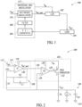
- Figure 1 is a voltage regulator circuit 100 including a low-dropout regulator 102, a load circuit 104 coupled to the low-dropout regulator 102, a voltage-to-current converter 106 coupled to the load circuit 104, an RC filter 108 coupled to the voltage-to-current converter 106, and an operational amplifier (Op Amp) voltage buffer 110 coupled between the RC filter 106 and the low-dropout regulator 102.
- a voltage-to-current converter 106 coupled to the load circuit 104
- an RC filter 108 coupled to the voltage-to-current converter 106
- Op Amp operational amplifier
- a reference voltage V REF is inputted into the Op Amp 110 and the second input of the Op Amp 110 is coupled to V OUT through resistor R1 (see Figure 2 ).
- the output of the Op Amp 110 is coupled to a first, negative input of the low-dropout regulator 102.
- the low-dropout regulator 102 is also coupled to the positive input voltage V IN .
- the load circuit 104 is coupled to the output of the low-dropout regulator 102 and to an output voltage V OUT .
- the voltage-to-current converter 106, RC filter 108, and Op Amp voltage buffer 110 collectively comprise an inversion and modulation circuit 112.
- FIG. 2 is the voltage regulator circuit 100 of Figure 1 in greater detail.
- the inversion and modulation circuit 112 includes a first Op Amp A1, a first resistor R1, a second resistor R2, and a first capacitor C1.
- the first Op Amp A1 has a first positive voltage supply node 118, which is supplied by the positive input voltage V IN .
- the first Op Amp A1 has a first positive input 114.
- the reference voltage V REF is coupled to the first positive input 114 of the first Op Amp A1.
- the first Op Amp A1 also has a first negative input 116 and a first output 120.
- the first output 120 of the first Op Amp A1 is the reference voltage V REF once it has been buffered, a buffered reference voltage V REF-BUFF .
- the first capacitor C1 and the second resistor R2 are coupled in parallel and collectively form the RC filter 108.
- the RC filter 108 is coupled between the first output 120 of the first Op Amp A1 and the first negative input 116 of the first Op Amp A1.
- the first output 120 of the first Op Amp A1 is coupled to the first negative input 116, forming the Op Amp voltage buffer 110 of Figure 1 .
- the low-dropout regulator 102 is coupled to the output 120 of the first Op Amp A1.
- the low-dropout regulator 102 includes a second Op Amp A2 and a pass transistor 122.
- the second Op Amp A2 has a second positive voltage supply node 128, which is coupled to the positive input voltage V IN .
- the second Op Amp A2 has a second positive input 124 and a second negative input 130, the second negative input 130 being coupled directly to the output 120 of the first Op Amp A1. That is, the buffered reference voltage V REF-BUFF , which is the output of the Op Amp voltage buffer 110 of Figure 1 , is inputted into the second negative input 130.
- the second Op Amp A2 also has an output 126, which is directly coupled to a gate G of the pass transistor 122.
- a source S of the pass transistor 122 is coupled to the positive input voltage V IN and to the second positive voltage supply node 128 of the second Op Amp A2.
- the first positive voltage supply node 118, the second positive voltage supply node 128, and the source S of the pass transistor 122 are each coupled to one another and are each coupled to the positive input voltage V IN .
- the load circuit 104 includes a resistor circuit RL, a current sink IL, and an external capacitor C EXT , which are each coupled in parallel.
- the resistor circuit RL, current sink IL, and external capacitor C EXT are each coupled to a ground voltage 132.
- the current sink II represents the load current of the device, which is dynamic.
- the load circuit 204 is coupled to the pass transistor 222 of the low-dropout regulator 202. More specifically, the load circuit 204 is coupled to a drain D of the pass transistor 222. The load circuit 204 is also coupled to the output voltage V OUT and to second positive input 224 of the second Op Amp A2.
- the advantage of having the first capacitor C1 grounded is that, when the first capacitor C1 is formed using a MOS, it takes up a smaller area. Thus, the voltage regulator circuit 200 is smaller in size.
- the accuracy of the system is improved by the reference correction circuitry. Further, the solution is completely analog, and the stability of the circuit is not compromised by the small external capacitor C EXT .
- the present disclosure achieves improved load regulation over other known solutions without increasing the size of the external capacitor C EXT .
- the present disclosure includes a low-dropout regulator circuit comprising a first amplifier circuit with a positive input node, a negative input node, and an output node, and a pass transistor coupled to the output node of the first amplifier.
- a load circuit is coupled to the positive input node of the first amplifier circuit, the load circuit comprising a resistor circuit, a current sink, and an external capacitor.
- a buffer circuit is coupled to the negative input node of the first amplifier circuit, the buffer circuit comprising a second amplifier circuit with a positive input node, a negative input node, and an output node.
- the output node of the second amplifier circuit is coupled to the negative input node of the first amplifier circuit.
- a filter circuit is coupled between the output node of the second amplifier circuit and the negative input node of the second amplifier circuit, the filter circuit comprising a capacitor and a first resistor.
- a gate of the pass transistor is coupled directly to the output node of the first amplifier circuit.
- the capacitor and the first resistor of the filter circuit are coupled in parallel.
- the output of the second amplifier circuit is coupled directly to the negative input node of the first amplifier circuit.
- a second resistor is coupled between the filter circuit and the load circuit.
- the second resistor is coupled to the negative input node of the second amplifier circuit.
- the positive input node of the first amplifier circuit is coupled to the load circuit.
- Embodiments also include a circuit comprising a first amplifier circuit with a first positive input, a first negative input, and a first output.
- the circuit further comprises a second amplifier circuit with a second positive input, a second negative input coupled to the first output and the first negative input, and a second output.
- a load circuit is coupled between the second positive input and the second output and a pass transistor is coupled directly to the second output and coupled between the second output and the load circuit.
- a filter circuit is coupled between the first output and the first negative input.
- the load circuit includes a resistor circuit, a current sink, and an external capacitor.
- the filter circuit includes a first resistor and a first capacitor, the first resistor and the first capacitor being coupled in parallel.
- a second resistor is coupled between the filter circuit and the load circuit.
- a reference voltage is coupled to the first positive input.
- Embodiments also include a circuit comprising a first operational amplifier with a first positive voltage supply node, a first positive input, a first negative input, and a first output coupled to the first negative input.
- a reference voltage is coupled to the first positive input.
- the circuit further includes a second operational amplifier with a second positive voltage supply node, a second positive input, a second negative input coupled to the first output and the first negative input, and a second output.
- a load circuit is coupled between the second positive input and the second output and a pass transistor is coupled between the second output and the load circuit.
- a filter circuit is coupled between the first output and the second negative input.
- a first resistor is coupled between the first output and the first negative input.
- the filter circuit comprises a second resistor and a first capacitor.
- the second resistor is coupled directly between the first output and the second negative input.
- An input voltage is coupled to the first positive voltage supply node, the second positive voltage supply node, and a source of the pass transistor.
- the first capacitor is coupled to a ground voltage.
- the load circuit includes a resistor circuit, a current sink, and a second capacitor.
Landscapes
- Engineering & Computer Science (AREA)
- Physics & Mathematics (AREA)
- Electromagnetism (AREA)
- General Physics & Mathematics (AREA)
- Radar, Positioning & Navigation (AREA)
- Automation & Control Theory (AREA)
- Continuous-Control Power Sources That Use Transistors (AREA)
Abstract
The present disclosure is directed to a fully analog voltage regulator circuit with reference modulation (110). The voltage regulator circuit includes a low-dropout regulator (102), a voltage-to-current converter (106), a resistor-capacitor filter circuit (108), and an operational amplifier voltage buffer. The voltage regulator circuit minimizes dropout voltage of the circuit by comparing the output voltage of the voltage regulator to a reference voltage (V<sub>REF)</sub> and adjusting the output voltage of the op amp voltage buffer, accordingly. The voltage regulator circuit includes two operational amplifiers, wherein the negative input of a first of the two operational amplifiers is coupled to the negative input of a second of the two operational amplifiers through the resistor-capacitor filter circuit (108).
Description
- The present disclosure relates to a voltage regulator circuit including a low-dropout regulator and a resistor-capacitor (RC) filter.
- Voltage regulators are electronic devices designed to stabilize the output voltage of a circuit. There are several types of existing voltage regulators, including linear regulators and switching regulators. Several variations of each of these types of voltage regulators exist, such as low-dropout regulators, buck-boost switching regulators, and flyback switching regulators. These variations provide different trade-offs between efficiency, cost, output voltage range, output current capability, and complexity.
- However, known voltage regulators suffer from several key disadvantages. For example, to maintain accuracy at a high load current, known voltage regulators require a large off-chip capacitor, which is expensive and results in a lower bandwidth with respect to the change in the load. Lower bandwidth corresponds to an increase in the reaction time of the regulator in response to a change in the load current. When a smaller off-chip capacitor is used, the DC gain of the loop is compromised to maintain stability in the system. Additionally, to improve accuracy, some known voltage regulators utilize multiple comparators, which results in excessive power consumption and occupies a large amount of space. Lastly, when digital and analog circuitry is combined in a voltage regulator, stability of the two components may be more delicate and the circuitry may have a larger form factor.
- The present disclosure is directed to a fully analog voltage regulator circuit with reference modulation. More specifically, the voltage regulator circuit includes a low-dropout regulator, a voltage-to-current convert, a resistor-capacitor (RC) filter, and an operational amplifier (op amp) in inverting configuration.
- The voltage regulator minimizes dropout voltage of the circuit by comparing the output voltage of the voltage regulator to a reference voltage, then adjusting the output voltage of the op amp voltage buffer, accordingly. If there is no voltage difference between the reference voltage and the output voltage of the voltage regulator, the output voltage of the op amp buffer will be equal to the output voltage of the voltage regulator. If there is a voltage difference between the reference voltage and the output voltage of the voltage regulator, the output voltage of the op amp buffer will be increased by a voltage equal to the difference.
- The present disclosure overcomes the drawbacks of the prior art. The reference modulation circuitry is implemented as an inverting amplifier where the difference between the reference voltage and the output voltage of the voltage regulator is converted to a proportional current and added back to the reference voltage. The reference correction improves the accuracy of the system. Additionally, since the circuit is fully analog, the system is more accurate and stability verification is less complex than in a digital system. Lastly, since the off-chip capacitor does not need to be larger, the voltage regulator has improved load regulation without sacrificing bandwidth or cost.
- For a better understanding of the present disclosure, one or more embodiments will now be described by way of example only, with reference to the accompanying drawings. In the drawings, identical reference numbers identify similar elements or acts. In some figures, the structures are drawn exactly to scale. In other figures, the sizes and relative positions of elements in the drawings are not necessarily drawn to scale. For example, the sizes, shapes of various elements and angles may be enlarged and positioned in the figures to improve drawing legibility.
-
Figure 1 schematically shows a voltage regulator circuit with reference modulation. -
Figure 2 shows, schematically and in greater detail, the voltage regulator circuit ofFigure 1 . -
Figure 3 schematically shows a second embodiment of a voltage regulator circuit with reference modulation. -
Figure 1 is avoltage regulator circuit 100 including a low-dropout regulator 102, aload circuit 104 coupled to the low-dropout regulator 102, a voltage-to-current converter 106 coupled to theload circuit 104, anRC filter 108 coupled to the voltage-to-current converter 106, and an operational amplifier (Op Amp)voltage buffer 110 coupled between theRC filter 106 and the low-dropout regulator 102. - A reference voltage VREF is inputted into the
Op Amp 110 and the second input of theOp Amp 110 is coupled to VOUT through resistor R1 (seeFigure 2 ). The output of the OpAmp 110 is coupled to a first, negative input of the low-dropout regulator 102. The low-dropout regulator 102 is also coupled to the positive input voltage VIN. Theload circuit 104 is coupled to the output of the low-dropout regulator 102 and to an output voltage VOUT. - The voltage-to-
current converter 106,RC filter 108, and OpAmp voltage buffer 110 collectively comprise an inversion andmodulation circuit 112. -
Figure 2 is thevoltage regulator circuit 100 ofFigure 1 in greater detail. The inversion andmodulation circuit 112 includes a first Op Amp A1, a first resistor R1, a second resistor R2, and a first capacitor C1. The first Op Amp A1 has a first positivevoltage supply node 118, which is supplied by the positive input voltage VIN. The first Op Amp A1 has a firstpositive input 114. The reference voltage VREF is coupled to the firstpositive input 114 of the first Op Amp A1. The first Op Amp A1 also has a firstnegative input 116 and afirst output 120. Thefirst output 120 of the first Op Amp A1 is the reference voltage VREF once it has been buffered, a buffered reference voltage VREF-BUFF. - The first capacitor C1 and the second resistor R2 are coupled in parallel and collectively form the
RC filter 108. TheRC filter 108 is coupled between thefirst output 120 of the first Op Amp A1 and the firstnegative input 116 of the first Op Amp A1. Thus, thefirst output 120 of the first Op Amp A1 is coupled to the firstnegative input 116, forming the OpAmp voltage buffer 110 ofFigure 1 . - The low-
dropout regulator 102 is coupled to theoutput 120 of the first Op Amp A1. The low-dropout regulator 102 includes a second Op Amp A2 and apass transistor 122. The second Op Amp A2 has a second positivevoltage supply node 128, which is coupled to the positive input voltage VIN. The second Op Amp A2 has a secondpositive input 124 and a secondnegative input 130, the secondnegative input 130 being coupled directly to theoutput 120 of the first Op Amp A1. That is, the buffered reference voltage VREF-BUFF, which is the output of the OpAmp voltage buffer 110 ofFigure 1 , is inputted into the secondnegative input 130. - The second Op Amp A2 also has an
output 126, which is directly coupled to a gate G of thepass transistor 122. A source S of thepass transistor 122 is coupled to the positive input voltage VIN and to the second positivevoltage supply node 128 of the second Op Amp A2. - The first positive
voltage supply node 118, the second positivevoltage supply node 128, and the source S of thepass transistor 122 are each coupled to one another and are each coupled to the positive input voltage VIN. - The
load circuit 104 is coupled to thepass transistor 122 of the low-dropout regulator 102. More specifically, theload circuit 104 is coupled to a drain D of thepass transistor 122. Theload circuit 104 is also coupled to the output voltage VOUT and to secondpositive input 124 of the second Op Amp A2. It is noted that source and drain can be interchangeable and the specific use of source S and drain D are used to simplify the discussion. - The
load circuit 104 includes a resistor circuit RL, a current sink IL, and an external capacitor CEXT, which are each coupled in parallel. The resistor circuit RL, current sink IL, and external capacitor CEXT are each coupled to aground voltage 132. The current sink II, represents the load current of the device, which is dynamic. - The
load circuit 104 is coupled to the inversion andmodulation circuit 112 directly through the first resistor R1. The first resistor R1 is coupled between theload circuit 104 and the firstnegative input 116 of the first Op Amp A1. The first resistor R1 is also coupled between theload circuit 104 and theRC filter 108. - Additionally, the first
negative input 116 of the first Op Amp A1 is coupled to the secondnegative input 130 of the second Op Amp A2 through theRC filter 108. - The
voltage regulator circuit 100 of the present disclosure maintains both stability and regulation accuracy without sacrificing bandwidth or cost. When voltage regulators receive a load current that can have different values across a wide range, it is difficult to stabilize the system. Other known voltage regulators include a much larger external capacitor than the external capacitor CEXT of the present disclosure, which improves accuracy at a high load current, but a larger external capacitor increases the size and cost of the system while decreasing bandwidth. Thevoltage regulator circuit 100 of the present disclosure utilizes a smaller external capacitor CEXT, which allows the overall size of thevoltage regulator circuit 100 to remain small and the bandwidth to remain high. Higher bandwidth corresponds to a decrease in the reaction time of the regulator in response to a change in the load current. - Additionally, when other known voltage regulators use a smaller external capacitor, the DC (Direct Current) gain is compromised in exchange for a more stable system. The
voltage regulator circuit 100 of the present disclosure uses fully analog reference correction circuitry, which senses the drop in voltage between the output and input and corrects the reference voltage VREF, accordingly, to keep the output voltage VOUT unchanged. The reference correction circuitry is implemented as an inverting amplifier configuration where the change in the output voltage VOUT is converted into a proportional current and added to the reference voltage VREF. The reference correction circuitry of the present disclosure compromises neither the DC gain nor the stability of the circuit. -
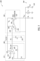
Figure 3 is an alternative embodiment of thevoltage regulator circuit 100 ofFigures 1 and 2 . Thevoltage regulator circuit 200 ofFigure 3 includes a low-dropout regulator 202, aload circuit 204, an inversion andmodulation circuit 212, and anRC filter 208. Unlike in the embodiment depicted inFigures 1 and 2 , theRC filter 208 of thevoltage regulator circuit 200 is not included in the inversion andmodulation circuit 212. Instead, the inversion andmodulation circuit 212 only includes an Op Amp voltage buffer and a voltage-to-current converter. - The inversion and
modulation circuit 112 includes a first Op Amp A1, a first resistor R1, and a second resistor R2. The first Op Amp A1 has a first positivevoltage supply node 218, which is coupled to a positive input voltage VIN. The first Op Amp A1 has a firstpositive input 214. The reference voltage VREF is coupled to the firstpositive input 214 of the first Op Amp A1. The first Op Amp A1 also has a firstnegative input 216 and afirst output 220. Thefirst output 220 of the first Op Amp A1 is the reference voltage VREF once it has been buffered VREF-BUFF. - The
first output 220 of the first Op Amp A1 is coupled to the firstnegative output 216 of the first Op Amp A1 through the second resistor R2. - The
RC filter 208 is coupled directly to thefirst output 220 of the first Op Amp A1. That is, the buffered reference voltage VREF-BUFF, which is the output of the OpAmp voltage buffer 110 ofFigure 1 , is inputted directly into theRC filter 208. - The
RC filter 208 includes a third resistor R3 and a first capacitor C1 (which can be formed by MOS and MOM), which are coupled in parallel. The third resistor R3 is coupled directly to thefirst output 220 of the first Op Amp A1. The first capacitor C1 is coupled to the third resistor R3 and coupled directly to aground voltage 232, which can be 0V. - The low-
dropout regulator 202 is coupled to theoutput 220 of the first Op Amp A1 through theRC filter 208. The low-dropout regulator 202 includes a second Op Amp A2 and apass transistor 222. The second Op Amp A2 has a second positivevoltage supply node 228, which is coupled to the positive input voltage VIN. The second Op Amp A2 has a secondpositive input 224 and a secondnegative input 230, the secondnegative input 230 being coupled directly to theRC filter 208. - The first
negative input 216 of the first Op Amp A1 is coupled to the secondnegative input 220 of the second Op Amp A2 through theRC filter 208 and the second resistor R2. The secondnegative input 220 of the second Op Amp A2 is coupled directly to the third resistor R3 of theRC filter 208. The first capacitor C1 is coupled between the third resistor R3 and the secondnegative input 220 of the second Op Amp A2. - The second Op Amp A2 also has a
second output 226, which is directly coupled to a gate G of thepass transistor 222. A source S of thepass transistor 222 is coupled to the positive input voltage VIN and to the second positivevoltage supply node 228 of the second Op Amp A2. - The first positive
voltage supply node 218, the second positivevoltage supply node 228, and the source S of thepass transistor 222 are each coupled to one another and are each coupled to the positive input voltage VIN. - The
load circuit 204 is coupled to thepass transistor 222 of the low-dropout regulator 202. More specifically, theload circuit 204 is coupled to a drain D of thepass transistor 222. Theload circuit 204 is also coupled to the output voltage VOUT and to secondpositive input 224 of the second Op Amp A2. - The
load circuit 204 includes a resistor circuit RL, a current sink IL, and an external capacitor CEXT, which are each coupled in parallel. The resistor circuit RL, current sink IL, and external capacitor CEXT are each coupled to theground voltage 232. - The
load circuit 204 is coupled to the inversion andmodulation circuit 212 directly through the first resistor R1. The first resistor R1 is coupled between theload circuit 204 and the firstnegative input 216 of the first Op Amp A1. The first resistor R1 is also coupled between theload circuit 204 and the second resistor R2. - The first capacitor C1 can be formed using a MOS (metal-oxide-semiconductor) transistor. The first capacitor C1 can be formed using a MOM (metal-oxide-metal) transistor.
- While the performance of the
voltage regulator circuit 200 ofFigure 3 is similar to the performance of thevoltage regulator circuit 100 inFigures 1 and 2 , the advantage of having the first capacitor C1 grounded is that, when the first capacitor C1 is formed using a MOS, it takes up a smaller area. Thus, thevoltage regulator circuit 200 is smaller in size. - There are many advantages of the architecture of the present disclosure. First, the accuracy of the system is improved by the reference correction circuitry. Further, the solution is completely analog, and the stability of the circuit is not compromised by the small external capacitor CEXT. The present disclosure achieves improved load regulation over other known solutions without increasing the size of the external capacitor CEXT.
- The present disclosure includes a low-dropout regulator circuit comprising a first amplifier circuit with a positive input node, a negative input node, and an output node, and a pass transistor coupled to the output node of the first amplifier. A load circuit is coupled to the positive input node of the first amplifier circuit, the load circuit comprising a resistor circuit, a current sink, and an external capacitor. A buffer circuit is coupled to the negative input node of the first amplifier circuit, the buffer circuit comprising a second amplifier circuit with a positive input node, a negative input node, and an output node. The output node of the second amplifier circuit is coupled to the negative input node of the first amplifier circuit. A filter circuit is coupled between the output node of the second amplifier circuit and the negative input node of the second amplifier circuit, the filter circuit comprising a capacitor and a first resistor.
- A gate of the pass transistor is coupled directly to the output node of the first amplifier circuit. The capacitor and the first resistor of the filter circuit are coupled in parallel. The output of the second amplifier circuit is coupled directly to the negative input node of the first amplifier circuit.
- A second resistor is coupled between the filter circuit and the load circuit. The second resistor is coupled to the negative input node of the second amplifier circuit. The positive input node of the first amplifier circuit is coupled to the load circuit.
- Embodiments also include a circuit comprising a first amplifier circuit with a first positive input, a first negative input, and a first output. The circuit further comprises a second amplifier circuit with a second positive input, a second negative input coupled to the first output and the first negative input, and a second output. A load circuit is coupled between the second positive input and the second output and a pass transistor is coupled directly to the second output and coupled between the second output and the load circuit. A filter circuit is coupled between the first output and the first negative input.
- The load circuit includes a resistor circuit, a current sink, and an external capacitor. The filter circuit includes a first resistor and a first capacitor, the first resistor and the first capacitor being coupled in parallel. A second resistor is coupled between the filter circuit and the load circuit. A reference voltage is coupled to the first positive input.
- Embodiments also include a circuit comprising a first operational amplifier with a first positive voltage supply node, a first positive input, a first negative input, and a first output coupled to the first negative input. A reference voltage is coupled to the first positive input. The circuit further includes a second operational amplifier with a second positive voltage supply node, a second positive input, a second negative input coupled to the first output and the first negative input, and a second output. A load circuit is coupled between the second positive input and the second output and a pass transistor is coupled between the second output and the load circuit. A filter circuit is coupled between the first output and the second negative input.
- A first resistor is coupled between the first output and the first negative input. The filter circuit comprises a second resistor and a first capacitor. The second resistor is coupled directly between the first output and the second negative input. An input voltage is coupled to the first positive voltage supply node, the second positive voltage supply node, and a source of the pass transistor.
- The first capacitor is coupled to a ground voltage. The load circuit includes a resistor circuit, a current sink, and a second capacitor.
- The various embodiments described above can be combined to provide further embodiments. Aspects of the embodiments can be modified, if necessary to employ concepts of the various patents, applications and publications to provide yet further embodiments.
- These and other changes can be made to the embodiments in light of the above-detailed description. In general, in the following claims, the terms used should not be construed to limit the claims to the specific embodiments disclosed in the specification and the claims, but should be construed to include all possible embodiments along with the full scope of equivalents to which such claims are entitled. Accordingly, the claims are not limited by the disclosure.
Claims (15)
- A device (100, 200), comprising:a low-dropout regulator circuit (102, 202), comprising:an amplifier circuit (A2) with a positive input node (124, 224), a negative input node (130, 230), and an output node (126, 226); anda pass transistor (122, 222) coupled to the output node (126, 226) of the amplifier circuit (A2);a load circuit (104, 204) coupled to the positive input node (124, 224) of the amplifier circuit (A2), the load circuit comprising;a resistor circuit (RL);a current sink (IL); andan load capacitor (CEXT);a buffer circuit coupled to the negative input node (130, 230) of the amplifier circuit (A2), the buffer circuit comprising:
a further amplifier circuit (A1) with a positive input node (114, 214), a negative input node (116, 216), and an output node (126, 226), the output node (126, 226) of the further amplifier circuit (A1) being coupled to the negative input node (130, 230) of the amplifier circuit (A2); anda filter circuit (108, 208) coupled between the output node (120, 220) of the further amplifier circuit (A1) and the negative input node (116, 216) of the further amplifier circuit, the filter circuit comprising a capacitor (C1) and a filter resistor (R2, R3). - The device (100, 200) of claim 1, wherein a gate (G) of the pass transistor (122, 222) is coupled directly to the output node (126, 226) of the amplifier circuit (A2).
- The device (100) of claim 1:wherein the capacitor (C1) and the filter resistor (R2) of the filter circuit are coupled in parallel, and/orwherein the output node (120) of the further amplifier circuit (A1) is coupled directly to the negative input node (130) of the amplifier circuit (A2).
- The device (100) of claim 1, further comprising a further resistor (R1) coupled between the filter circuit (108) and the load circuit (104, 204), wherein the further resistor (R1) is preferably coupled to the negative input node (116) of the further amplifier circuit (A1).
- The device (100, 200) of claim 1, wherein the positive input node (124, 224) of the amplifier circuit (A2) is coupled to the load circuit (104, 204).
- A circuit (100, 200) comprising:a first amplifier circuit (A1) with a first positive input (114, 214), a first negative input (116, 216), and a first output (120, 220);a second amplifier circuit (A2) with a second positive input (124, 224), a second negative input (130, 230) coupled to the first output (120, 220) and the first negative input (116, 216), and a second output (126, 226);a load circuit (104, 204) coupled between the second positive input (124, 224) and the second output (126, 226);a pass transistor (126, 226) coupled directly to the second output (126, 226) and coupled between the second output (126, 226) and the load circuit (104, 204); anda filter circuit (108, 208) coupled between the first output (120, 220) and the first negative input (116, 126).
- The circuit (100, 200) of claim 6, wherein the load circuit (104, 204) includes a resistor circuit (RL), a current sink (IL), and a load capacitor (CEXT).
- The circuit (100, 200) of claim 6, wherein the filter circuit (108, 208) includes a filter resistor (R2, R3) and a first capacitor (C1), wherein, preferably, the filter resistor (R2) and the first capacitor (C1) are coupled in parallel.
- The circuit (100, 200) of claim 6:
wherein a further resistor (R1) is coupled between the filter circuit (108, 208) and the load circuit (104, 204); and/or.
wherein a reference voltage (VREF) is coupled to the first positive input (114, 214). - A circuit (100, 200) comprising:a first operational amplifier (A1) with a first positive voltage supply node (118, 218), a first positive input (114, 214), a first negative input (116, 216), and a first output (120, 220) coupled to the first negative input (116, 216);a reference voltage (VREF) coupled to the first positive input (114, 214);a second operational amplifier (A2) with a second positive voltage supply node (128, 228), a second positive input (124, 224), a second negative input (130, 230) coupled to the first output (120, 220) and the first negative input (116, 216), and a second output (126, 226);a load circuit (104, 204) coupled between the second positive input (124, 224) and the second output (126, 226);a pass transistor (122, 222) coupled between the second output (126, 226) and the load circuit (104, 204); anda filter circuit (108, 208) coupled between the first output (120, 220) and the second negative input (130, 230).
- The circuit (100, 200) of claim 10, wherein a resistor (R2) is coupled between the first output (120, 220) and the first negative input (116, 216).
- The circuit (100, 200) of claim 11, wherein the filter circuit (108, 208) comprises a further resistor (R2, R3) and a first capacitor (C1).
- The circuit (100, 200) of claim 12, wherein the further resistor (R3) is coupled directly between the first output (220) and the second negative input (230).
- The circuit (100, 200) of claim 10, wherein an input voltage is coupled to the first positive voltage supply node (118, 218), the second positive voltage supply node (128, 228), and a source of the pass transistor (122, 222).
- The circuit (100, 200) of claim 12:wherein the first capacitor (C1) is coupled to a ground voltage (232); and/orwherein the load circuit (104, 204) includes a resistor circuit (RL), a current sink (IL), and a second capacitor (CEXT).
Applications Claiming Priority (1)
| Application Number | Priority Date | Filing Date | Title |
|---|---|---|---|
| US18/326,876 US12487617B2 (en) | 2023-05-31 | 2023-05-31 | Analog voltage regulator with reference modulation |
Publications (1)
| Publication Number | Publication Date |
|---|---|
| EP4471533A1 true EP4471533A1 (en) | 2024-12-04 |
Family
ID=91193523
Family Applications (1)
| Application Number | Title | Priority Date | Filing Date |
|---|---|---|---|
| EP24177009.8A Pending EP4471533A1 (en) | 2023-05-31 | 2024-05-21 | Analog voltage regulator with reference modulation |
Country Status (3)
| Country | Link |
|---|---|
| US (1) | US12487617B2 (en) |
| EP (1) | EP4471533A1 (en) |
| CN (2) | CN119065436A (en) |
Citations (3)
| Publication number | Priority date | Publication date | Assignee | Title |
|---|---|---|---|---|
| US20030214275A1 (en) * | 2002-05-20 | 2003-11-20 | Biagi Hubert J. | Low drop-out regulator having current feedback amplifier and composite feedback loop |
| US7397226B1 (en) * | 2005-01-13 | 2008-07-08 | National Semiconductor Corporation | Low noise, low power, fast startup, and low drop-out voltage regulator |
| US7589507B2 (en) * | 2005-12-30 | 2009-09-15 | St-Ericsson Sa | Low dropout regulator with stability compensation |
Family Cites Families (12)
| Publication number | Priority date | Publication date | Assignee | Title |
|---|---|---|---|---|
| US6806690B2 (en) | 2001-12-18 | 2004-10-19 | Texas Instruments Incorporated | Ultra-low quiescent current low dropout (LDO) voltage regulator with dynamic bias and bandwidth |
| US9753480B2 (en) | 2013-08-09 | 2017-09-05 | Stmicroelectronics International N.V. | Voltage regulators |
| US9405309B2 (en) | 2014-11-29 | 2016-08-02 | Infineon Technologies Ag | Dual mode low-dropout linear regulator |
| KR102204678B1 (en) | 2014-12-11 | 2021-01-20 | 삼성전자주식회사 | Dual loop voltage regulator based on inverter amplfier and therefore voltage regulating method |
| US20180120879A1 (en) * | 2016-10-27 | 2018-05-03 | Qualcomm Incorporated | Voltage regulator with enhanced power supply rejection ratio and load-transient performance |
| US10146240B1 (en) | 2018-02-01 | 2018-12-04 | Apple Inc. | High current LDO voltage regulator with dynamic pre-regulator |
| US10185344B1 (en) * | 2018-06-01 | 2019-01-22 | Semiconductor Components Industries, Llc | Compensation of input current of LDO output stage |
| US10771017B2 (en) * | 2019-01-08 | 2020-09-08 | Elite Semiconductor Memory Technology Inc. | Amplifier circuit with low malfunction rate |
| US10996699B2 (en) | 2019-07-30 | 2021-05-04 | Stmicroelectronics Asia Pacific Pte Ltd | Low drop-out (LDO) voltage regulator circuit |
| US11231732B1 (en) * | 2020-07-07 | 2022-01-25 | Cirrus Logic, Inc. | Pre-charge management for power-managed voltage references |
| US11599132B2 (en) * | 2021-02-26 | 2023-03-07 | Nuvoton Technology Corporation | Method and apparatus for reducing power-up overstress of capacitor-less regulating circuits |
| US11789478B2 (en) * | 2022-02-22 | 2023-10-17 | Credo Technology Group Limited | Voltage regulator with supply noise cancellation |
-
2023
- 2023-05-31 US US18/326,876 patent/US12487617B2/en active Active
-
2024
- 2024-05-17 CN CN202410612741.9A patent/CN119065436A/en active Pending
- 2024-05-17 CN CN202421075378.3U patent/CN222734427U/en active Active
- 2024-05-21 EP EP24177009.8A patent/EP4471533A1/en active Pending
Patent Citations (3)
| Publication number | Priority date | Publication date | Assignee | Title |
|---|---|---|---|---|
| US20030214275A1 (en) * | 2002-05-20 | 2003-11-20 | Biagi Hubert J. | Low drop-out regulator having current feedback amplifier and composite feedback loop |
| US7397226B1 (en) * | 2005-01-13 | 2008-07-08 | National Semiconductor Corporation | Low noise, low power, fast startup, and low drop-out voltage regulator |
| US7589507B2 (en) * | 2005-12-30 | 2009-09-15 | St-Ericsson Sa | Low dropout regulator with stability compensation |
Also Published As
| Publication number | Publication date |
|---|---|
| US12487617B2 (en) | 2025-12-02 |
| US20240402738A1 (en) | 2024-12-05 |
| CN222734427U (en) | 2025-04-08 |
| CN119065436A (en) | 2024-12-03 |
Similar Documents
| Publication | Publication Date | Title |
|---|---|---|
| CN106292824B (en) | Low-dropout regulator circuit | |
| CN114840051B (en) | Low power consumption, high transient response, capacitor-free low dropout linear regulator | |
| US8860395B2 (en) | Circuit and method for generating a ramp compensation voltage for a switching regulator | |
| US10411599B1 (en) | Boost and LDO hybrid converter with dual-loop control | |
| CN203982247U (en) | High-performance reference source | |
| US20060055383A1 (en) | Adaptive biasing concept for current mode voltage regulators | |
| EP4240111B1 (en) | Control circuit and lighting device | |
| US7498771B2 (en) | Battery charging device with voltage-balanced transistors | |
| CN213634248U (en) | Enhancement type buffer suitable for LDO circuit and LDO circuit thereof | |
| US20220382308A1 (en) | Voltage regulator | |
| CN217484784U (en) | Low-power-consumption high-transient-response low-dropout linear voltage regulator without off-chip capacitor | |
| WO2016119658A1 (en) | Power factor correction circuit, multiplier and voltage feed-forward circuit | |
| CN115167599A (en) | Low dropout linear regulator | |
| US12328067B2 (en) | Regulator with flipped voltage follower architecture | |
| US12487617B2 (en) | Analog voltage regulator with reference modulation | |
| CN116149411A (en) | Low Dropout Linear Regulator Circuit | |
| CN102393781A (en) | Low-dropout linear voltage regulator circuit and system | |
| CN203982254U (en) | Self-starting band gap reference | |
| US11916486B2 (en) | Type-2 compensation with reduced quiescent current | |
| CN116088622B (en) | Soft-start circuits, low-dropout linear regulators, chips and electronic equipment | |
| CN118034449A (en) | A low power consumption low voltage dropout linear regulator with dynamic gate voltage regulation | |
| CN115528787B (en) | Control loop accelerating circuit | |
| CN101510724B (en) | Low voltage output circuit | |
| CN113098416B (en) | Operational amplifier circuit and switching power supply | |
| CN113541482B (en) | Linear regulator and power supply device |
Legal Events
| Date | Code | Title | Description |
|---|---|---|---|
| PUAI | Public reference made under article 153(3) epc to a published international application that has entered the european phase |
Free format text: ORIGINAL CODE: 0009012 |
|
| STAA | Information on the status of an ep patent application or granted ep patent |
Free format text: STATUS: THE APPLICATION HAS BEEN PUBLISHED |
|
| AK | Designated contracting states |
Kind code of ref document: A1 Designated state(s): AL AT BE BG CH CY CZ DE DK EE ES FI FR GB GR HR HU IE IS IT LI LT LU LV MC ME MK MT NL NO PL PT RO RS SE SI SK SM TR |
|
| STAA | Information on the status of an ep patent application or granted ep patent |
Free format text: STATUS: REQUEST FOR EXAMINATION WAS MADE |
|
| 17P | Request for examination filed |
Effective date: 20250318 |