EP4468829A1 - Printed circuit board assembly - Google Patents
Printed circuit board assembly Download PDFInfo
- Publication number
- EP4468829A1 EP4468829A1 EP23175182.7A EP23175182A EP4468829A1 EP 4468829 A1 EP4468829 A1 EP 4468829A1 EP 23175182 A EP23175182 A EP 23175182A EP 4468829 A1 EP4468829 A1 EP 4468829A1
- Authority
- EP
- European Patent Office
- Prior art keywords
- pcb
- circuit board
- printed circuit
- electronic component
- terminals
- Prior art date
- Legal status (The legal status is an assumption and is not a legal conclusion. Google has not performed a legal analysis and makes no representation as to the accuracy of the status listed.)
- Pending
Links
Images


Classifications
-
- H—ELECTRICITY
- H05—ELECTRIC TECHNIQUES NOT OTHERWISE PROVIDED FOR
- H05K—PRINTED CIRCUITS; CASINGS OR CONSTRUCTIONAL DETAILS OF ELECTRIC APPARATUS; MANUFACTURE OF ASSEMBLAGES OF ELECTRICAL COMPONENTS
- H05K1/00—Printed circuits
- H05K1/02—Details
- H05K1/11—Printed elements for providing electric connections to or between printed circuits
- H05K1/115—Via connections; Lands around holes or via connections
-
- H—ELECTRICITY
- H05—ELECTRIC TECHNIQUES NOT OTHERWISE PROVIDED FOR
- H05K—PRINTED CIRCUITS; CASINGS OR CONSTRUCTIONAL DETAILS OF ELECTRIC APPARATUS; MANUFACTURE OF ASSEMBLAGES OF ELECTRICAL COMPONENTS
- H05K1/00—Printed circuits
- H05K1/02—Details
- H05K1/0271—Arrangements for reducing stress or warp in rigid printed circuit boards, e.g. caused by loads, vibrations or differences in thermal expansion
-
- H—ELECTRICITY
- H05—ELECTRIC TECHNIQUES NOT OTHERWISE PROVIDED FOR
- H05K—PRINTED CIRCUITS; CASINGS OR CONSTRUCTIONAL DETAILS OF ELECTRIC APPARATUS; MANUFACTURE OF ASSEMBLAGES OF ELECTRICAL COMPONENTS
- H05K1/00—Printed circuits
- H05K1/02—Details
- H05K1/11—Printed elements for providing electric connections to or between printed circuits
- H05K1/111—Pads for surface mounting, e.g. lay-out
-
- H—ELECTRICITY
- H05—ELECTRIC TECHNIQUES NOT OTHERWISE PROVIDED FOR
- H05K—PRINTED CIRCUITS; CASINGS OR CONSTRUCTIONAL DETAILS OF ELECTRIC APPARATUS; MANUFACTURE OF ASSEMBLAGES OF ELECTRICAL COMPONENTS
- H05K1/00—Printed circuits
- H05K1/18—Printed circuits structurally associated with non-printed electric components
- H05K1/181—Printed circuits structurally associated with non-printed electric components associated with surface mounted components
-
- H—ELECTRICITY
- H05—ELECTRIC TECHNIQUES NOT OTHERWISE PROVIDED FOR
- H05K—PRINTED CIRCUITS; CASINGS OR CONSTRUCTIONAL DETAILS OF ELECTRIC APPARATUS; MANUFACTURE OF ASSEMBLAGES OF ELECTRICAL COMPONENTS
- H05K1/00—Printed circuits
- H05K1/18—Printed circuits structurally associated with non-printed electric components
- H05K1/182—Printed circuits structurally associated with non-printed electric components associated with components mounted in printed circuit boards [PCB], e.g. insert-mounted components [IMC]
- H05K1/184—Printed circuits structurally associated with non-printed electric components associated with components mounted in printed circuit boards [PCB], e.g. insert-mounted components [IMC] associated with components inserted in holes through the PCBs and wherein terminals of the components are connected to printed contacts on the walls of the holes or at the edges thereof or protruding over or into the holes
-
- H—ELECTRICITY
- H05—ELECTRIC TECHNIQUES NOT OTHERWISE PROVIDED FOR
- H05K—PRINTED CIRCUITS; CASINGS OR CONSTRUCTIONAL DETAILS OF ELECTRIC APPARATUS; MANUFACTURE OF ASSEMBLAGES OF ELECTRICAL COMPONENTS
- H05K3/00—Apparatus or processes for manufacturing printed circuits
- H05K3/30—Assembling printed circuits with electric components, e.g. with resistors
- H05K3/32—Assembling printed circuits with electric components, e.g. with resistors electrically connecting electric components or wires to printed circuits
- H05K3/34—Assembling printed circuits with electric components, e.g. with resistors electrically connecting electric components or wires to printed circuits by soldering
- H05K3/341—Surface mounted components
- H05K3/3431—Leadless components
- H05K3/3436—Leadless components having an array of bottom contacts, e.g. pad grid array or ball grid array components
-
- H—ELECTRICITY
- H05—ELECTRIC TECHNIQUES NOT OTHERWISE PROVIDED FOR
- H05K—PRINTED CIRCUITS; CASINGS OR CONSTRUCTIONAL DETAILS OF ELECTRIC APPARATUS; MANUFACTURE OF ASSEMBLAGES OF ELECTRICAL COMPONENTS
- H05K2201/00—Indexing scheme relating to printed circuits covered by H05K1/00
- H05K2201/09—Shape and layout
- H05K2201/09009—Substrate related
- H05K2201/09063—Holes or slots in insulating substrate not used for electrical connections
-
- H—ELECTRICITY
- H05—ELECTRIC TECHNIQUES NOT OTHERWISE PROVIDED FOR
- H05K—PRINTED CIRCUITS; CASINGS OR CONSTRUCTIONAL DETAILS OF ELECTRIC APPARATUS; MANUFACTURE OF ASSEMBLAGES OF ELECTRICAL COMPONENTS
- H05K2201/00—Indexing scheme relating to printed circuits covered by H05K1/00
- H05K2201/09—Shape and layout
- H05K2201/09009—Substrate related
- H05K2201/09072—Hole or recess under component or special relationship between hole and component
-
- H—ELECTRICITY
- H05—ELECTRIC TECHNIQUES NOT OTHERWISE PROVIDED FOR
- H05K—PRINTED CIRCUITS; CASINGS OR CONSTRUCTIONAL DETAILS OF ELECTRIC APPARATUS; MANUFACTURE OF ASSEMBLAGES OF ELECTRICAL COMPONENTS
- H05K2201/00—Indexing scheme relating to printed circuits covered by H05K1/00
- H05K2201/09—Shape and layout
- H05K2201/09009—Substrate related
- H05K2201/09136—Means for correcting warpage
-
- H—ELECTRICITY
- H05—ELECTRIC TECHNIQUES NOT OTHERWISE PROVIDED FOR
- H05K—PRINTED CIRCUITS; CASINGS OR CONSTRUCTIONAL DETAILS OF ELECTRIC APPARATUS; MANUFACTURE OF ASSEMBLAGES OF ELECTRICAL COMPONENTS
- H05K2201/00—Indexing scheme relating to printed circuits covered by H05K1/00
- H05K2201/09—Shape and layout
- H05K2201/09209—Shape and layout details of conductors
- H05K2201/095—Conductive through-holes or vias
- H05K2201/09545—Plated through-holes or blind vias without lands
-
- H—ELECTRICITY
- H05—ELECTRIC TECHNIQUES NOT OTHERWISE PROVIDED FOR
- H05K—PRINTED CIRCUITS; CASINGS OR CONSTRUCTIONAL DETAILS OF ELECTRIC APPARATUS; MANUFACTURE OF ASSEMBLAGES OF ELECTRICAL COMPONENTS
- H05K2201/00—Indexing scheme relating to printed circuits covered by H05K1/00
- H05K2201/09—Shape and layout
- H05K2201/09209—Shape and layout details of conductors
- H05K2201/09654—Shape and layout details of conductors covering at least two types of conductors provided for in H05K2201/09218 - H05K2201/095
- H05K2201/09781—Dummy conductors, i.e. not used for normal transport of current; Dummy electrodes of components
-
- H—ELECTRICITY
- H05—ELECTRIC TECHNIQUES NOT OTHERWISE PROVIDED FOR
- H05K—PRINTED CIRCUITS; CASINGS OR CONSTRUCTIONAL DETAILS OF ELECTRIC APPARATUS; MANUFACTURE OF ASSEMBLAGES OF ELECTRICAL COMPONENTS
- H05K2201/00—Indexing scheme relating to printed circuits covered by H05K1/00
- H05K2201/10—Details of components or other objects attached to or integrated in a printed circuit board
- H05K2201/10007—Types of components
- H05K2201/10151—Sensor
-
- H—ELECTRICITY
- H05—ELECTRIC TECHNIQUES NOT OTHERWISE PROVIDED FOR
- H05K—PRINTED CIRCUITS; CASINGS OR CONSTRUCTIONAL DETAILS OF ELECTRIC APPARATUS; MANUFACTURE OF ASSEMBLAGES OF ELECTRICAL COMPONENTS
- H05K2201/00—Indexing scheme relating to printed circuits covered by H05K1/00
- H05K2201/10—Details of components or other objects attached to or integrated in a printed circuit board
- H05K2201/10613—Details of electrical connections of non-printed components, e.g. special leads
- H05K2201/10621—Components characterised by their electrical contacts
- H05K2201/10636—Leadless chip, e.g. chip capacitor or resistor
-
- H—ELECTRICITY
- H05—ELECTRIC TECHNIQUES NOT OTHERWISE PROVIDED FOR
- H05K—PRINTED CIRCUITS; CASINGS OR CONSTRUCTIONAL DETAILS OF ELECTRIC APPARATUS; MANUFACTURE OF ASSEMBLAGES OF ELECTRICAL COMPONENTS
- H05K2201/00—Indexing scheme relating to printed circuits covered by H05K1/00
- H05K2201/10—Details of components or other objects attached to or integrated in a printed circuit board
- H05K2201/10613—Details of electrical connections of non-printed components, e.g. special leads
- H05K2201/10621—Components characterised by their electrical contacts
- H05K2201/10659—Different types of terminals for the same component, e.g. solder balls combined with leads
-
- H—ELECTRICITY
- H05—ELECTRIC TECHNIQUES NOT OTHERWISE PROVIDED FOR
- H05K—PRINTED CIRCUITS; CASINGS OR CONSTRUCTIONAL DETAILS OF ELECTRIC APPARATUS; MANUFACTURE OF ASSEMBLAGES OF ELECTRICAL COMPONENTS
- H05K2201/00—Indexing scheme relating to printed circuits covered by H05K1/00
- H05K2201/10—Details of components or other objects attached to or integrated in a printed circuit board
- H05K2201/10613—Details of electrical connections of non-printed components, e.g. special leads
- H05K2201/10621—Components characterised by their electrical contacts
- H05K2201/10689—Leaded Integrated Circuit [IC] package, e.g. dual-in-line [DIL]
Definitions
- the invention relates to a printed circuit board (PCB) assembly comprising a printed circuit board (PCB); an electronic component mounted on the PCB at a mounting portion thereof, the electronic component having a plurality of electrical connection terminals for soldering to corresponding connection locations of the PCB and the mounting portion having an aperture facing the electronic component mounted on the PCB.
- PCB printed circuit board
- the printed circuit board has a tendency to expand by the absorption of humidity, e.g., environmental humidity and/or heat, e.g., heat dissipated from the electronic component. Since this expansion behaviour is generally different from the one of the electronic component and since the latter one has its electrical connection terminals fixedly soldered to the connection locations on the PCB, mechanical stresses may occur in the components' connection terminals and may thereby cause an instability of the components' electrical characteristics. This is specifically undesirable for components serving as a voltage reference for an electronic measurement sensor, specifically a load cell.
- humidity e.g., environmental humidity and/or heat, e.g., heat dissipated from the electronic component. Since this expansion behaviour is generally different from the one of the electronic component and since the latter one has its electrical connection terminals fixedly soldered to the connection locations on the PCB, mechanical stresses may occur in the components' connection terminals and may thereby cause an instability of the components' electrical characteristics. This is specifically undesirable for components serving as a voltage reference for an electronic measurement sensor, specifically a load cell.
- the aperture in the mounting portion has been provided in prior art proposals in order to reduce dissipation of heat into the PCB. There are, however, applications where the improvement that is attained by the provision of this aperture is not sufficient.
- this object is obtained with a printed circuit board assembly of the before referenced type, wherein at least one of the terminals is unconnected and the aperture extends into a region of the PCB that faces the at least one unconnected terminal.
- PCB printed circuit board
- the inventors have recognized that stress on the terminals because of different expansions of the PCB and the component as a result of an exposure to heat and/or humidity could theoretically be reduced by the provision of separating slots at the mounting portion of the PCB that extend between corresponding connection locations of the PCB. This is, however, practically not feasible since the distance between neighbouring connection locations of the PCB is as small as the distance between the facing connection terminals of the component, and this small distance would not allow to cut the slots with available PCB to link equipment.
- connection terminals of the electronic component have not assigned an electrical function thereto so that there is from a perspective of electrical function no need to solder these terminals to the corresponding connection locations of the PCB.
- at least one of the terminals having no electrical function is not soldered to the corresponding connection location of the PCB and the aperture of the PCB is configured to extend into a region of the PCB that faces the at least one unconnected terminal. In this way, the aperture may extend over the whole width between second nearest connection locations on the PCB and may thus be easily machined with available PCB machining tools.
- the electrical connection terminals are arranged along the four sides of a rectangle with a first unconnected terminal located on a center line between two opposing sides of the rectangle and second and third unconnected terminals located opposite to each other in a direction that is orthogonal to the center line, and the aperture comprises first, second and third proximally contiguous branches distally facing the first, second and third unconnected terminals, respectively.
- each of the first, second and third branches may extend along a first, second and third rectilinear center line, respectively, having a constant width in the orthogonal direction thereto.
- the distal end portions of the first, second and third branches, respectively may extend outwardly beyond the area of the PCB that faces the rectangle.
- the first center line of the first branch may coincide with the center line between the opposing sides of the rectangle and the second and third center lines may intersect in one single intersection point. Further, the angles between the center line between the opposing sides of the rectangle and the second and third rectilinear center lines, respectively, may be the same. In this way, when these angles are essentially 90°, the first, second and third rectilinear center lines are in the shape of a T. When these angles are less than 90°, the first, second and third rectilinear center lines are in the shape of a Y.
- the electronic component is a voltage source for supplying a reference voltage for an electronic measurement sensor.
- the measurement sensor is a load sensor.
- Voltage sources for supplying a reference voltage referred to in brief as voltage references, play a key role in the performance of the measurement sensor, in particular the load sensor or load cell. These voltage references set the precision standard. Configuring the aperture in accordance with the invention, considerably increases the stability of the voltage reference and thereby results in higher precision.
- the electronic component is a surface mount technology (SMT) component.
- SMT surface mount technology
- the connection locations of the PCB and the connection terminals of the electronic component are preferably in the form of soldering pads.
- the invention is also applicable in through-hole-technology (THT), wherein rigid pins of the electric component are soldered into conductive holes formed in the PCB.
- the aperture is plated.
- the plating covers at least the edge of the aperture in the thickness direction of the PCB to thereby form a seal against the penetration of humidity.
- Suitable plating materials include copper and/or gold.
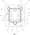
- a printed circuit board assembly 10 comprises a printed circuit board (PCB) 20 and an electronic component 30 mounted thereon at a mounting portion thereof.
- Figs. 1 to 3 illustrate a corresponding detail of the printed circuit board assembly 10.
- the electronic component 30 is schematically illustrated in Fig. 1 showing the upper side of the PCB 20 as a rectangle represented as a thick black line.
- Fig. 2 showing the opposite lower side portions of the rectangle that are not visible from the lower side are illustrated as dashed lines.
- the PCB 20 has a Y-shaped aperture 24 formed therein that is represented in Fig. 2 as a bold black line.
- Fig. 1 portions covered by the electronic component 30 are illustrated as dashed lines.
- aperture 24 is composed of a first branch 24' that extends along a rectilinear center line that coincides with a center line of the rectangle that extends parallel to its opposing sides 34, and of second and third branches 24", 24′′′, each having a rectilinear center line extending under the same angles in relation to the rectilinear center line of the first branch 24'.
- Each of the first, second and third branches 24', 24", and 24′′′ is of constant width in the direction that is orthogonal to its center line.
- the first, second and third branches 24', 24", 24′′′ join at their proximal ends. Their distal ends project beyond the inside of the rectangle to the outside thereof.
- Figures 1 and 2 further show rectangular connection locations 22 of the PCB 20. Two of them face and are soldered to the connection terminals of the electronic component 30 that are located on the right side of the first branch 24', while further two of them face and are soldered to the two connection terminals located at the left side of the first branch 24'.
- a further connection location of the PCB 20 faces and is soldered to a connection terminal of the electronic component 30 that is located between the second and third branches 24" and 24′′′.
- connection terminals 32', 32", and 32′′′ that face the first, second and third branches 24', 24", 24′′′, respectively, are unconnected.
- connection terminal 32' located at the left and right sides 34, 34 of the electronic component 30 connected by soldering 50 to the facing connection locations 22 of the PCB 20.
- connection terminal 32' located midway therebetween is freely exposed to the first branch 24' of aperture 24 and is unconnected.
- the edge of the aperture 24 that extends between the upper side and the lower side of the PCB 20 in the thickness direction thereof is represented as a bold line. This is to schematically indicate a plating with an appropriate material, e.g., copper and/or gold, to seal the PCB against penetrating moisture. This coating may also further extend over adjacent regions on the upper and lower sides of the PCB 20.
Landscapes
- Engineering & Computer Science (AREA)
- Microelectronics & Electronic Packaging (AREA)
- Manufacturing & Machinery (AREA)
- Structures For Mounting Electric Components On Printed Circuit Boards (AREA)
- Electric Connection Of Electric Components To Printed Circuits (AREA)
- Structure Of Printed Boards (AREA)
Abstract
Printed circuit board (PCB) assembly 10 comprising a printed circuit board (PCB) 20; an electronic component 30 mounted on the PCB 20 at a mounting portion thereof, the electronic component 30 having a plurality of electrical connection terminals 32; 32' for soldering to corresponding connection locations 22 of the PCB 20 and the mounting portion having an aperture 24 facing the electronic component 30 mounted on the PCB 20; wherein at least one of the terminals 32' is unconnected and the aperture 24 extends into a region of the PCB 20 that faces the at least one unconnected terminal 32'.
Description
- The invention relates to a printed circuit board (PCB) assembly comprising a printed circuit board (PCB); an electronic component mounted on the PCB at a mounting portion thereof, the electronic component having a plurality of electrical connection terminals for soldering to corresponding connection locations of the PCB and the mounting portion having an aperture facing the electronic component mounted on the PCB.
- In printed circuit board assemblies of the above referenced type the printed circuit board (PCB) has a tendency to expand by the absorption of humidity, e.g., environmental humidity and/or heat, e.g., heat dissipated from the electronic component. Since this expansion behaviour is generally different from the one of the electronic component and since the latter one has its electrical connection terminals fixedly soldered to the connection locations on the PCB, mechanical stresses may occur in the components' connection terminals and may thereby cause an instability of the components' electrical characteristics. This is specifically undesirable for components serving as a voltage reference for an electronic measurement sensor, specifically a load cell.
- To alleviate this problem, the aperture in the mounting portion has been provided in prior art proposals in order to reduce dissipation of heat into the PCB. There are, however, applications where the improvement that is attained by the provision of this aperture is not sufficient.
- It is thus an object of the present invention to provide a printed circuit board assembly of the above referenced type in which the electrical stability is further improved.
- In accordance with the invention, this object is obtained with a printed circuit board assembly of the before referenced type, wherein at least one of the terminals is unconnected and the aperture extends into a region of the PCB that faces the at least one unconnected terminal.
- Electronic components designed for mounting on a printed circuit board (PCB) normally have the electrical connection terminals thereof arranged in linear rows with only a small distance between neighbouring terminals of the row. The inventors have recognized that stress on the terminals because of different expansions of the PCB and the component as a result of an exposure to heat and/or humidity could theoretically be reduced by the provision of separating slots at the mounting portion of the PCB that extend between corresponding connection locations of the PCB. This is, however, practically not feasible since the distance between neighbouring connection locations of the PCB is as small as the distance between the facing connection terminals of the component, and this small distance would not allow to cut the slots with available PCB to link equipment. At the same time, the inventors have considered that in many applications one or more connection terminals of the electronic component have not assigned an electrical function thereto so that there is from a perspective of electrical function no need to solder these terminals to the corresponding connection locations of the PCB. According to the invention, at least one of the terminals having no electrical function is not soldered to the corresponding connection location of the PCB and the aperture of the PCB is configured to extend into a region of the PCB that faces the at least one unconnected terminal. In this way, the aperture may extend over the whole width between second nearest connection locations on the PCB and may thus be easily machined with available PCB machining tools.
- In an advantageous embodiment of the printed circuit board assembly, the electrical connection terminals are arranged along the four sides of a rectangle with a first unconnected terminal located on a center line between two opposing sides of the rectangle and second and third unconnected terminals located opposite to each other in a direction that is orthogonal to the center line, and the aperture comprises first, second and third proximally contiguous branches distally facing the first, second and third unconnected terminals, respectively. In particular, each of the first, second and third branches may extend along a first, second and third rectilinear center line, respectively, having a constant width in the orthogonal direction thereto. The distal end portions of the first, second and third branches, respectively, may extend outwardly beyond the area of the PCB that faces the rectangle. The first center line of the first branch may coincide with the center line between the opposing sides of the rectangle and the second and third center lines may intersect in one single intersection point. Further, the angles between the center line between the opposing sides of the rectangle and the second and third rectilinear center lines, respectively, may be the same. In this way, when these angles are essentially 90°, the first, second and third rectilinear center lines are in the shape of a T. When these angles are less than 90°, the first, second and third rectilinear center lines are in the shape of a Y.
- In expedient embodiments, the second and third unconnected terminals may be each located adjacent to a corner of the rectangle. Further, each of the two opposing sides may have three terminals equidistantly located therealong and each of the remaining sides that extend in the direction orthogonally thereto has one terminal located at mid-length thereof.
- According to another aspect of the invention, the electronic component is a voltage source for supplying a reference voltage for an electronic measurement sensor. Specifically, the measurement sensor is a load sensor. Voltage sources for supplying a reference voltage, referred to in brief as voltage references, play a key role in the performance of the measurement sensor, in particular the load sensor or load cell. These voltage references set the precision standard. Configuring the aperture in accordance with the invention, considerably increases the stability of the voltage reference and thereby results in higher precision.
- In preferred embodiments, the electronic component is a surface mount technology (SMT) component. In this case, the connection locations of the PCB and the connection terminals of the electronic component are preferably in the form of soldering pads. Alternatively, the invention is also applicable in through-hole-technology (THT), wherein rigid pins of the electric component are soldered into conductive holes formed in the PCB.
- According to a further aspect of the invention, the aperture is plated. The plating covers at least the edge of the aperture in the thickness direction of the PCB to thereby form a seal against the penetration of humidity. Suitable plating materials include copper and/or gold.
- In the following, an exemplary embodiment of the invention is described with reference to the drawings. These drawings show:
- Fig. 1
- a plan view of the upper side of a printed circuit board that has an electronic component mounted thereon;
- Fig. 2
- a plan view of the lower side of the printed circuit board that is opposite to the one of
Fig. 1 ; and - Fig. 3
- a cross-sectional view according to the line X-X in
Figs. 1 and2 . - A printed
circuit board assembly 10 comprises a printed circuit board (PCB) 20 and anelectronic component 30 mounted thereon at a mounting portion thereof.Figs. 1 to 3 illustrate a corresponding detail of the printedcircuit board assembly 10. Theelectronic component 30 is schematically illustrated inFig. 1 showing the upper side of thePCB 20 as a rectangle represented as a thick black line. InFig. 2 showing the opposite lower side portions of the rectangle that are not visible from the lower side are illustrated as dashed lines. - In the illustrated embodiment, the
electronic component 30 comprises eight square-shaped connection terminals electronic component 30 that faces the upper side ofPCB 20. Each of twosides 34 of the rectangle has three of theconnection terminals opposing sides - The PCB 20 has a Y-
shaped aperture 24 formed therein that is represented inFig. 2 as a bold black line. InFig. 1 portions covered by theelectronic component 30 are illustrated as dashed lines. As may be seen fromFigs. 1 and2 ,aperture 24 is composed of a first branch 24' that extends along a rectilinear center line that coincides with a center line of the rectangle that extends parallel to itsopposing sides 34, and of second andthird branches 24", 24‴, each having a rectilinear center line extending under the same angles in relation to the rectilinear center line of the first branch 24'. Each of the first, second andthird branches 24', 24", and 24‴ is of constant width in the direction that is orthogonal to its center line. The first, second andthird branches 24', 24", 24‴ join at their proximal ends. Their distal ends project beyond the inside of the rectangle to the outside thereof. -
Figures 1 and2 further showrectangular connection locations 22 of thePCB 20. Two of them face and are soldered to the connection terminals of theelectronic component 30 that are located on the right side of the first branch 24', while further two of them face and are soldered to the two connection terminals located at the left side of the first branch 24'. In addition, a further connection location of thePCB 20 faces and is soldered to a connection terminal of theelectronic component 30 that is located between the second andthird branches 24" and 24‴. In contrast,connection terminals 32', 32", and 32‴ that face the first, second andthird branches 24', 24", 24‴, respectively, are unconnected. - This is illustrated in more detail in
Fig. 3 for the lowermost connection terminal 32' and its nearest neighbours inFig. 1 . The cross-sectional view ofFig. 3 shows the twoconnection terminals 32 located at the left andright sides electronic component 30 connected by soldering 50 to the facingconnection locations 22 of the PCB 20. In contrast, connection terminal 32' located midway therebetween is freely exposed to the first branch 24' ofaperture 24 and is unconnected. - The edge of the
aperture 24 that extends between the upper side and the lower side of thePCB 20 in the thickness direction thereof is represented as a bold line. This is to schematically indicate a plating with an appropriate material, e.g., copper and/or gold, to seal the PCB against penetrating moisture. This coating may also further extend over adjacent regions on the upper and lower sides of thePCB 20. -
- 10
- printed circuit board assembly
- 20
- printed circuit board (PCB)
- 22
- connection location
- 24
- aperture
- 24'; 24"; 24‴
- branch
- 30
- electronic component
- 32; 32'; 32"; 32‴
- connection terminal
- 34
- side of rectangle
- 50
- solder
Claims (8)
- Printed circuit board (PCB) assembly (10) comprisinga printed circuit board (PCB) (20);an electronic component (30) mounted on the PCB (20) at a mounting portion thereof, the electronic component (30) having a plurality of electrical connection terminals (32; 32') for soldering to corresponding connection locations (22) of the PCB (20) and the mounting portion having an aperture (24) facing the electronic component (30) mounted on the PCB (20);wherein at least one of the terminals (32') is unconnected and the aperture (24) extends into a region of the PCB (20) that faces the at least one unconnected terminal (32').
- Printed circuit board assembly according to claim 1, wherein the electrical connection terminals (32; 32'; 32"; 32‴) are arranged along the four sides of a rectangle with a first unconnected terminal (32') located on a center line between two opposing sides (34) of the rectangle and second and third unconnected terminals (32"; 32‴) located opposite to each other in a direction that is orthogonal to the center line, and the aperture (24) comprises first, second and third proximally contiguous branches (24'; 24"; 24‴) distally facing the first, second and third unconnected terminals (32'; 32"; 32‴), respectively.
- Printed circuit board assembly according to claim 2, wherein the second and third unconnected terminals (32"; 32‴) are each located adjacent to a corner of the rectangle.
- Printed circuit board assembly according to anyone of claims 2 and 3, wherein each of the two opposing sides has three terminals (32; 32'; 32"; 32‴) equidistantly located therealong and each of the remaining sides that extend in the direction orthogonal thereto has one terminal located at mid-length thereof.
- Printed circuit board assembly according to anyone of the preceding claims, wherein the electronic component (30) is a voltage source for supplying a reference voltage for an electronic measurement sensor.
- Printed circuit board assembly according to claim 5, wherein the measurement sensor is a load sensor.
- Printed circuit board assembly according to anyone of the preceding claims, wherein the electronic component (30) is a surface mount technology (SMT) component.
- Printed circuit board assembly according to anyone of the preceding claims, wherein the aperture (24; 24'; 24"; 24‴) is plated.
Priority Applications (4)
| Application Number | Priority Date | Filing Date | Title |
|---|---|---|---|
| EP23175182.7A EP4468829A1 (en) | 2023-05-24 | 2023-05-24 | Printed circuit board assembly |
| US18/652,893 US20240397614A1 (en) | 2023-05-24 | 2024-05-02 | Printed circuit board assembly |
| CN202410609092.7A CN119031577A (en) | 2023-05-24 | 2024-05-16 | Printed Circuit Board Assembly |
| JP2024083493A JP2024169381A (en) | 2023-05-24 | 2024-05-22 | Printed Circuit Board Assembly |
Applications Claiming Priority (1)
| Application Number | Priority Date | Filing Date | Title |
|---|---|---|---|
| EP23175182.7A EP4468829A1 (en) | 2023-05-24 | 2023-05-24 | Printed circuit board assembly |
Publications (1)
| Publication Number | Publication Date |
|---|---|
| EP4468829A1 true EP4468829A1 (en) | 2024-11-27 |
Family
ID=86603933
Family Applications (1)
| Application Number | Title | Priority Date | Filing Date |
|---|---|---|---|
| EP23175182.7A Pending EP4468829A1 (en) | 2023-05-24 | 2023-05-24 | Printed circuit board assembly |
Country Status (4)
| Country | Link |
|---|---|
| US (1) | US20240397614A1 (en) |
| EP (1) | EP4468829A1 (en) |
| JP (1) | JP2024169381A (en) |
| CN (1) | CN119031577A (en) |
Citations (4)
| Publication number | Priority date | Publication date | Assignee | Title |
|---|---|---|---|---|
| EP0083265A1 (en) * | 1981-12-22 | 1983-07-06 | Socapex | Interconnection carrier on a printed circuit for an integrated-circuit housing, and interconnection system utilizing such a carrier |
| US4641222A (en) * | 1984-05-29 | 1987-02-03 | Motorola, Inc. | Mounting system for stress relief in surface mounted components |
| EP2519084A1 (en) * | 2009-12-24 | 2012-10-31 | Furukawa Electric Co., Ltd. | Assembly structure for injection molded substrate and for mounting component |
| JP2014056992A (en) * | 2012-09-13 | 2014-03-27 | Sumitomo Bakelite Co Ltd | Electronic device and electronic device manufacturing method |
Family Cites Families (3)
| Publication number | Priority date | Publication date | Assignee | Title |
|---|---|---|---|---|
| DE19810060B4 (en) * | 1997-05-07 | 2005-10-13 | Fraunhofer-Gesellschaft zur Förderung der angewandten Forschung e.V. | A method of connecting a device to a substrate and an electrical circuit made therewith |
| DE102017204842A1 (en) * | 2017-03-22 | 2018-09-27 | Robert Bosch Gmbh | Contact configuration |
| CN112838743B (en) * | 2019-11-22 | 2022-03-29 | 英业达科技有限公司 | Power supply device |
-
2023
- 2023-05-24 EP EP23175182.7A patent/EP4468829A1/en active Pending
-
2024
- 2024-05-02 US US18/652,893 patent/US20240397614A1/en active Pending
- 2024-05-16 CN CN202410609092.7A patent/CN119031577A/en active Pending
- 2024-05-22 JP JP2024083493A patent/JP2024169381A/en active Pending
Patent Citations (4)
| Publication number | Priority date | Publication date | Assignee | Title |
|---|---|---|---|---|
| EP0083265A1 (en) * | 1981-12-22 | 1983-07-06 | Socapex | Interconnection carrier on a printed circuit for an integrated-circuit housing, and interconnection system utilizing such a carrier |
| US4641222A (en) * | 1984-05-29 | 1987-02-03 | Motorola, Inc. | Mounting system for stress relief in surface mounted components |
| EP2519084A1 (en) * | 2009-12-24 | 2012-10-31 | Furukawa Electric Co., Ltd. | Assembly structure for injection molded substrate and for mounting component |
| JP2014056992A (en) * | 2012-09-13 | 2014-03-27 | Sumitomo Bakelite Co Ltd | Electronic device and electronic device manufacturing method |
Also Published As
| Publication number | Publication date |
|---|---|
| CN119031577A (en) | 2024-11-26 |
| US20240397614A1 (en) | 2024-11-28 |
| JP2024169381A (en) | 2024-12-05 |
Similar Documents
| Publication | Publication Date | Title |
|---|---|---|
| JPS62229896A (en) | Printed wiring board | |
| US4882656A (en) | Surface mounted decoupling capacitor | |
| EP1450404A2 (en) | Assembly in pressure contact with a power semiconductor module | |
| KR20030060882A (en) | Semiconductor device and semiconductor module | |
| US8089140B2 (en) | Lead frame assembly, lead frame and insulating housing combination, and led module having the same | |
| EP1473802B1 (en) | Tab terminal | |
| JP2000223183A (en) | Electrical connector | |
| US20240397614A1 (en) | Printed circuit board assembly | |
| EP0878987A1 (en) | Printed circuit board | |
| US5030110A (en) | Case assembly for stacking integrated circuit packages | |
| US5616034A (en) | Power supply apparatus for package | |
| JPH03181191A (en) | Printed wiring board | |
| CA1069198A (en) | Laminated programmable microstrip interconnector | |
| US5534667A (en) | Printed circuit board having zig-zag contact arrangement | |
| KR100380784B1 (en) | Integrated circuit comprising fuse links which can be separated by the action of energy | |
| JPH07230862A (en) | Printed circuit board pin header | |
| US20260047001A1 (en) | Mounting substrate and mounting structure | |
| US12550259B2 (en) | Electrically coupling printed circuit boards using a snap-fit connector | |
| EP0976155B1 (en) | High-voltage, high-current multilayer circuit board, method for the production thereof | |
| JPH0766543A (en) | Printed board | |
| US7059867B1 (en) | High density multi-lead surface mount interconnect and devices including same | |
| JPH0427195Y2 (en) | ||
| JP3004397B2 (en) | Flexible printed circuit board | |
| US10965079B2 (en) | Comb pattern insert for wave solder pallets | |
| DE202023002819U1 (en) | printed circuit board assembly |
Legal Events
| Date | Code | Title | Description |
|---|---|---|---|
| PUAI | Public reference made under article 153(3) epc to a published international application that has entered the european phase |
Free format text: ORIGINAL CODE: 0009012 |
|
| STAA | Information on the status of an ep patent application or granted ep patent |
Free format text: STATUS: THE APPLICATION HAS BEEN PUBLISHED |
|
| AK | Designated contracting states |
Kind code of ref document: A1 Designated state(s): AL AT BE BG CH CY CZ DE DK EE ES FI FR GB GR HR HU IE IS IT LI LT LU LV MC ME MK MT NL NO PL PT RO RS SE SI SK SM TR |
|
| STAA | Information on the status of an ep patent application or granted ep patent |
Free format text: STATUS: REQUEST FOR EXAMINATION WAS MADE |
|
| 17P | Request for examination filed |
Effective date: 20250516 |