EP4468366A1 - Halbleitervorrichtung und verfahren zu deren herstellung - Google Patents
Halbleitervorrichtung und verfahren zu deren herstellung Download PDFInfo
- Publication number
- EP4468366A1 EP4468366A1 EP24155654.7A EP24155654A EP4468366A1 EP 4468366 A1 EP4468366 A1 EP 4468366A1 EP 24155654 A EP24155654 A EP 24155654A EP 4468366 A1 EP4468366 A1 EP 4468366A1
- Authority
- EP
- European Patent Office
- Prior art keywords
- region
- electrode
- semiconductor
- fluorine
- insulating
- Prior art date
- Legal status (The legal status is an assumption and is not a legal conclusion. Google has not performed a legal analysis and makes no representation as to the accuracy of the status listed.)
- Granted
Links
Images




Classifications
-
- H—ELECTRICITY
- H10—SEMICONDUCTOR DEVICES; ELECTRIC SOLID-STATE DEVICES NOT OTHERWISE PROVIDED FOR
- H10D—INORGANIC ELECTRIC SEMICONDUCTOR DEVICES
- H10D30/00—Field-effect transistors [FET]
- H10D30/40—FETs having zero-dimensional [0D], one-dimensional [1D] or two-dimensional [2D] charge carrier gas channels
- H10D30/47—FETs having zero-dimensional [0D], one-dimensional [1D] or two-dimensional [2D] charge carrier gas channels having two-dimensional [2D] charge carrier gas channels, e.g. nanoribbon FETs or high electron mobility transistors [HEMT]
- H10D30/471—High electron mobility transistors [HEMT] or high hole mobility transistors [HHMT]
- H10D30/475—High electron mobility transistors [HEMT] or high hole mobility transistors [HHMT] having wider bandgap layer formed on top of lower bandgap active layer, e.g. undoped barrier HEMTs such as i-AlGaN/GaN HEMTs
-
- H—ELECTRICITY
- H10—SEMICONDUCTOR DEVICES; ELECTRIC SOLID-STATE DEVICES NOT OTHERWISE PROVIDED FOR
- H10D—INORGANIC ELECTRIC SEMICONDUCTOR DEVICES
- H10D62/00—Semiconductor bodies, or regions thereof, of devices having potential barriers
- H10D62/10—Shapes, relative sizes or dispositions of the regions of the semiconductor bodies; Shapes of the semiconductor bodies
- H10D62/102—Constructional design considerations for preventing surface leakage or controlling electric field concentration
-
- H—ELECTRICITY
- H10—SEMICONDUCTOR DEVICES; ELECTRIC SOLID-STATE DEVICES NOT OTHERWISE PROVIDED FOR
- H10D—INORGANIC ELECTRIC SEMICONDUCTOR DEVICES
- H10D62/00—Semiconductor bodies, or regions thereof, of devices having potential barriers
- H10D62/80—Semiconductor bodies, or regions thereof, of devices having potential barriers characterised by the materials
- H10D62/82—Heterojunctions
- H10D62/824—Heterojunctions comprising only Group III-V materials heterojunctions, e.g. GaN/AlGaN heterojunctions
-
- H—ELECTRICITY
- H10—SEMICONDUCTOR DEVICES; ELECTRIC SOLID-STATE DEVICES NOT OTHERWISE PROVIDED FOR
- H10D—INORGANIC ELECTRIC SEMICONDUCTOR DEVICES
- H10D62/00—Semiconductor bodies, or regions thereof, of devices having potential barriers
- H10D62/80—Semiconductor bodies, or regions thereof, of devices having potential barriers characterised by the materials
- H10D62/85—Semiconductor bodies, or regions thereof, of devices having potential barriers characterised by the materials being Group III-V materials, e.g. GaAs
- H10D62/8503—Nitride Group III-V materials, e.g. AlN or GaN
-
- H—ELECTRICITY
- H10—SEMICONDUCTOR DEVICES; ELECTRIC SOLID-STATE DEVICES NOT OTHERWISE PROVIDED FOR
- H10D—INORGANIC ELECTRIC SEMICONDUCTOR DEVICES
- H10D64/00—Electrodes of devices having potential barriers
- H10D64/111—Field plates
- H10D64/112—Field plates comprising multiple field plate segments
-
- H—ELECTRICITY
- H10—SEMICONDUCTOR DEVICES; ELECTRIC SOLID-STATE DEVICES NOT OTHERWISE PROVIDED FOR
- H10D—INORGANIC ELECTRIC SEMICONDUCTOR DEVICES
- H10D64/00—Electrodes of devices having potential barriers
- H10D64/20—Electrodes characterised by their shapes, relative sizes or dispositions
- H10D64/23—Electrodes carrying the current to be rectified, amplified, oscillated or switched, e.g. sources, drains, anodes or cathodes
- H10D64/251—Source or drain electrodes for field-effect devices
- H10D64/256—Source or drain electrodes for field-effect devices for lateral devices wherein the source or drain electrodes are recessed in semiconductor bodies
-
- H—ELECTRICITY
- H10—SEMICONDUCTOR DEVICES; ELECTRIC SOLID-STATE DEVICES NOT OTHERWISE PROVIDED FOR
- H10D—INORGANIC ELECTRIC SEMICONDUCTOR DEVICES
- H10D64/00—Electrodes of devices having potential barriers
- H10D64/20—Electrodes characterised by their shapes, relative sizes or dispositions
- H10D64/27—Electrodes not carrying the current to be rectified, amplified, oscillated or switched, e.g. gates
- H10D64/311—Gate electrodes for field-effect devices
- H10D64/411—Gate electrodes for field-effect devices for FETs
- H10D64/511—Gate electrodes for field-effect devices for FETs for IGFETs
- H10D64/512—Disposition of the gate electrodes, e.g. buried gates
- H10D64/513—Disposition of the gate electrodes, e.g. buried gates within recesses in the substrate, e.g. trench gates, groove gates or buried gates
-
- H—ELECTRICITY
- H10—SEMICONDUCTOR DEVICES; ELECTRIC SOLID-STATE DEVICES NOT OTHERWISE PROVIDED FOR
- H10D—INORGANIC ELECTRIC SEMICONDUCTOR DEVICES
- H10D64/00—Electrodes of devices having potential barriers
- H10D64/60—Electrodes characterised by their materials
- H10D64/66—Electrodes having a conductor capacitively coupled to a semiconductor by an insulator, e.g. MIS electrodes
- H10D64/68—Electrodes having a conductor capacitively coupled to a semiconductor by an insulator, e.g. MIS electrodes characterised by the insulator, e.g. by the gate insulator
- H10D64/693—Electrodes having a conductor capacitively coupled to a semiconductor by an insulator, e.g. MIS electrodes characterised by the insulator, e.g. by the gate insulator the insulator comprising nitrogen, e.g. nitrides, oxynitrides or nitrogen-doped materials
-
- H—ELECTRICITY
- H10—SEMICONDUCTOR DEVICES; ELECTRIC SOLID-STATE DEVICES NOT OTHERWISE PROVIDED FOR
- H10D—INORGANIC ELECTRIC SEMICONDUCTOR DEVICES
- H10D30/00—Field-effect transistors [FET]
- H10D30/01—Manufacture or treatment
- H10D30/015—Manufacture or treatment of FETs having heterojunction interface channels or heterojunction gate electrodes, e.g. HEMT
-
- H—ELECTRICITY
- H10—SEMICONDUCTOR DEVICES; ELECTRIC SOLID-STATE DEVICES NOT OTHERWISE PROVIDED FOR
- H10D—INORGANIC ELECTRIC SEMICONDUCTOR DEVICES
- H10D64/00—Electrodes of devices having potential barriers
- H10D64/20—Electrodes characterised by their shapes, relative sizes or dispositions
- H10D64/27—Electrodes not carrying the current to be rectified, amplified, oscillated or switched, e.g. gates
- H10D64/311—Gate electrodes for field-effect devices
- H10D64/411—Gate electrodes for field-effect devices for FETs
- H10D64/511—Gate electrodes for field-effect devices for FETs for IGFETs
- H10D64/517—Gate electrodes for field-effect devices for FETs for IGFETs characterised by the conducting layers
- H10D64/518—Gate electrodes for field-effect devices for FETs for IGFETs characterised by the conducting layers characterised by their lengths or sectional shapes
Definitions
- Embodiments described herein generally relate to a semiconductor device and a method for manufacturing the same device.
- a semiconductor device includes a first electrode, a second electrode, a third electrode, a first semiconductor region, and a second semiconductor region.
- the first electrode extends in a first direction.
- the second electrode extends in the first direction.
- a second direction from the first electrode to the second electrode is perpendicular to the first direction.
- the third electrode extends in the first direction.
- a position of the third electrode in the second direction is between a position of the first electrode in the second direction and a position of the second electrode in the second direction.
- the first semiconductor region includes Al x1 Ga 1-x1 N (0 ⁇ x1 ⁇ 1).
- the first semiconductor region includes a first partial region, a second partial region, a third partial region, a fourth partial region, and a fifth partial region.
- a third direction from the first partial region to the first electrode crosses a plane including the first direction and the second direction.
- a direction from the second partial region to the second electrode is along the third direction.
- a direction from the third partial region to the third electrode is along the third direction.
- a position of the fourth partial region in the second direction is between a position of the first partial region in the second direction and a position of the third partial region in the second direction.
- a position of the fifth partial region in the second direction is between the position of the third partial region in the second direction and a position of the second partial region in the second direction.
- the second semiconductor region includes Al x2 Ga 1-x2 N (0 ⁇ x2 ⁇ 1, x1 ⁇ x2).
- the second semiconductor region includes a first semiconductor portion and a second semiconductor portion.
- a direction from the fourth partial region to the first semiconductor portion is along the third direction.
- a direction from the fifth partial region to the second semiconductor portion is along the third direction.
- the second semiconductor portion includes a first region and a second region.
- a position of the first region in the second direction is between a position of the second region in the second direction and the position of the second electrode in the second direction.
- a concentration of fluorine in the first region is higher than a concentration of fluorine in the second region.
- the first region includes fluorine and the second region does not include fluorine.
- FIG. 1 is a schematic plan view illustrating a semiconductor device according to a first embodiment.
- FIG. 2 is a schematic cross-sectional view illustrating the semiconductor device according to the first embodiment.
- FIG. 2 is a cross-sectional view taken along the line A1-A2 of FIG. 1 .
- a semiconductor device 110 includes a first electrode 51, a second electrode 52, a third electrode 53, a first semiconductor region 10 and a second semiconductor region 20.
- the first electrode 51, the second electrode 52, and the third electrode 53 extend in a first direction D1.
- a second direction D2 from the first electrode 51 to the second electrode 52 is perpendicular to the first direction D1.
- the first direction D1 is a Y-axis direction.
- One direction perpendicular to the Y-axis direction is defined as an X-axis direction.
- a direction perpendicular to the Y-axis direction and the X-axis direction is defined as a Z-axis direction.
- the second direction D2 is the X-axis direction.
- a length of the first electrode 51 in the first direction D1 is longer than a length (width) of the first electrode 51 in the second direction D2.
- a length of the second electrode 52 in the first direction D1 is longer than a length (width) of the second electrode 52 in the second direction D2.
- a length of the third electrode 53 in the first direction D1 is longer than a length (width) of the third electrode 53 in the second direction D2.
- the first electrode 51, the second electrode 52 and the third electrode 53 are stripes extending in the first direction.
- a position of the third electrode 53 in the second direction D2 is between a position of the first electrode 51 in the second direction D2 and a position of the second electrode 52 in the second direction D2.
- the first semiconductor region 10 includes Al x1 Ga 1-x1 N (0 ⁇ x1 ⁇ 1).
- the composition ratio x1 is, for example, not less than 0 and not more than 0.1.
- the first semiconductor region 10 is, for example, a GaN layer.
- the first semiconductor region 10 includes a first partial region 11, a second partial region 12, a third partial region 13, a fourth partial region 14 and a fifth partial region 15.
- a third direction D3 from the first partial region 11 to the first electrode 51 crosses a plane including the first direction D1 and the second direction D2.
- the third direction D3 is, for example, the Z-axis direction.
- a direction from the second partial region 12 to the second electrode 52 is along the third direction D3.
- a direction from the third partial region 13 to the third electrode 53 is along the third direction D3.
- the first partial region 11 overlaps the first electrode 51 in the third direction D3.
- the second partial region 12 overlaps the second electrode 52 in the third direction D3.
- the third partial region 13 overlaps the third electrode 53 in the third direction D3.
- a position of the fourth partial region 14 in the second direction D2 is between a position of the first partial region 11 in the second direction D2 and a position of the third partial region 13 in the second direction D2.
- a position of the fifth partial region 15 in the second direction D2 is between a position of the third partial region 13 in the second direction D2 and a position of the second partial region 12 in the second direction D2.
- the second semiconductor region 20 includes Al x2 Ga 1-x2 N (0 ⁇ x2 ⁇ 1, x1 ⁇ x2).
- the composition ratio x2 is, for example, not less than 0.2 and not more than 0.35.
- the second semiconductor region 20 is, for example, an AlGaN layer.
- the second semiconductor region 20 includes a first semiconductor portion 21 and a second semiconductor portion 22. A direction from the fourth partial region 14 to the first semiconductor portion 21 is along the third direction D3. A direction from the fifth partial region 15 to the second semiconductor portion 22 is along the third direction D3.
- the second semiconductor portion 22 includes a first region 22a and a second region 22b.
- a position of the first region 22a in the second direction D2 is between a position of the second region 22b in the second direction D2 and a position of the second electrode 52 in the second direction D2.
- a concentration of fluorine in the first region 22a is higher than a concentration of fluorine in the second region 22b.
- the first region 22a includes fluorine and the second region 22b does not include fluorine.
- a current flowing between the first electrode 51 and the second electrode 52 can be controlled by a potential of the third electrode 53.
- the potential of the third electrode 53 may be based on a potential of the first electrode 51.
- the first electrode 51 functions as a source electrode.
- the second electrode 52 functions as a drain electrode.
- the third electrode 53 functions as a gate electrode.
- the semiconductor device 110 is, for example, a transistor.
- the first semiconductor region 10 includes a portion facing the second semiconductor region 20.
- a carrier region 10c is formed in this portion.
- the carrier region 10c is, for example, a two-dimensional electron gas.
- the semiconductor device 110 is, for example, a HEMT (High Electron Mobility Transistor).
- the distance between the first electrode 51 and the third electrode 53 in the second direction D2 is shorter than the distance between the third electrode 53 and the second electrode 52 in the second direction D2. More stable characteristics can be obtained.
- a voltage applied to the second electrode 52 is higher than a voltage applied to the third electrode 53. Therefore, a high electric field is concentrated in a region near the second electrode 52, and the operation tends to become unstable. For example, traps are likely to be generated due to the high electric field generated at the end of the second electrode 52. This makes it easier for the characteristics to change, for example. For example, current collapse may occur.
- the first region 22a close to the second electrode 52 include fluorine.
- fluorine when fluorine is present in the first region 22a, the generation of traps is suppressed. This makes it easier to maintain stable characteristics even when a high electric field is concentrated in a region close to the second electrode 52. For example, current collapse is suppressed.
- a semiconductor device with improved characteristics can be provided.
- the second region 22b having a low concentration of fluorine or including no fluorine is provided.
- stable characteristics and low on-resistance can be obtained.
- FIG. 3 is a schematic cross-sectional view illustrating a part of the semiconductor device according to the first embodiment.
- FIG. 3 shows an enlarged example of a part of the semiconductor device 110 that includes the second electrode 52.
- the second electrode portion 52b is an eaves portion.
- the second electrode portion 52b may function as a field plate on the drain side. A high electric field tends to occur locally at the end of the second electrode portion 52b.
- a region 10F surrounded by a broken line includes fluorine. At least a part of the first region 22a is included in the region 10F.
- the boundary 22x between the second region 22b and the first region 22a is located between the third electrode 53 and the second electrode 52.
- the position of the boundary 22x in the second direction D2 is between the position of the third electrode 53 in the second direction D2 and the position of the second electrode portion 52b in the second direction D2.
- at least part of the first region 22a does not overlap the second electrode portion 52b in the third direction D3.
- a high electric field tends to concentrate at the end of the second electrode portion 52b on the third electrode 53 side.
- the second semiconductor portion 22 may further include a third region 22c.
- the third region 22c is located between the second partial region 12 and the first electrode portion 52a in the third direction D3.
- the concentration of fluorine in the third region 22c is lower than the concentration of fluorine in the first region 22a.
- the third region 22c does not include fluorine.
- low contact resistance can be obtained because the region overlapping the first electrode portion 52a does not include fluorine. This makes it easier to obtain low on-resistance.
- a region with a high fluorine concentration may be locally provided on the surface side of the second semiconductor portion 22. Traps that affect the characteristics tend to occur on the surface side of the second semiconductor portion 22.
- first region 22a a region with a high fluorine concentration
- second region 22a a region with a high fluorine concentration
- changes in characteristics can be effectively suppressed.
- fourth region 22d with a low fluorine concentration, for example, low on-resistance can be easily obtained.
- the semiconductor device 110 may further include a first insulating member 41. At least a part of the first insulating member 41 is located between the first region 22a and the second electrode portion 52b.
- a portion 41p of the first insulating member 41 is located between the first region 22a and the second electrode portion 52b. Another portion 41q of the first insulating member 41 does not overlap the second electrode 52 in the third direction D3.
- the thickness along the third direction D3 of the portion 41p of the first insulating member 41 is defined as a thickness t41p.
- the thickness along the third direction D3 of the other portion 41q of the first insulating member 41 is defined as a thickness t41q.
- the thickness t41p is thinner than the thickness t41q.
- the portion 41p of the first insulating member 41 overlaps the first region 22a. Even when such a difference in thickness is provided, stable characteristics can be effectively obtained by providing the first region 22a.
- the first insulating member 41 includes a first insulating portion 41a and a second insulating portion 41b. At least part of the first insulating portion 41a is located between the second semiconductor portion 22 and the second insulating portion 41b in the third direction D3. The first insulating portion 41a does not overlap the second electrode portion 52b in the third direction D3. A part of the second insulating portion 41b is located between the first region 22a and the second electrode portion 52b in the third direction D3. This part of the second insulating portion 41b is located between the first insulating portion 41a and the first electrode portion 52a in the second direction D2. In this way, a stacked structure may be applied to the first insulating member 41.
- the first insulating portion 41a can be formed by CVD (for example, LPCVD: Low-Pressure Chemical Vapor Deposition).
- the second insulating portion 41b can be formed, for example, by CVD (for example, PECVD: plasma-enhanced chemical vapor deposition).
- the film quality of the first insulating portion 41a is higher than the film quality of the second insulating portion 41b. It is easier to obtain more stable characteristics.
- the first insulating member 41 (the first insulating portion 41a and the second insulating portion 41b) may include silicon and nitrogen, for example.
- the first insulating portion 41a and the second insulating portion 41b include, for example, silicon nitride. It is easy to obtain stable characteristics.
- the first insulating member 41 (the first insulating portion 41a and the second insulating portion 41b) may include silicon and oxygen, for example.
- the third electrode 53 includes a third electrode portion 53c and a fourth electrode portion 53d.
- the third electrode portion 53c is in contact with a part of the first insulating portion 41a.
- the fourth electrode portion 53d is electrically connected to the third electrode portion 53c.
- the fourth electrode portion 53d is, for example, an eaves portion.
- the first electrode 51 includes a fifth electrode portion 51e and a sixth electrode portion 51f.
- the fifth electrode portion 51e is electrically connected to the first partial region 11 (and the first semiconductor portion 21).
- the sixth electrode portion 51f is electrically connected to the fifth electrode portion 51e.
- the sixth electrode portion 51f is, for example, an eaves portion.
- the semiconductor device 110 may include a base 18s and a nitride layer 18b.
- the first semiconductor region 10 is provided between the base 18 s and the second semiconductor region 20.
- the nitride layer 18b is provided between the base 18s and the first semiconductor region 10.
- the base 18s may be, for example, a silicon substrate.
- the nitride layer 18b includes, for example, Al, Ga, and nitrogen.
- the nitride layer 18b includes AlGaN, for example. This AlGaN layer is, for example, a buffer layer.
- the nitride layer 18b includes a region facing the first semiconductor region 10. This region may include a GaN layer including carbon.
- the on-resistance after the voltage stress test is three times the initial value before the voltage stress test.
- the on-resistance after the voltage stress test is six times the initial value before the voltage stress test.
- FIG. 4 is a schematic cross-sectional view illustrating a part of a semiconductor device according to the first embodiment.
- the first insulating member 41 includes the first insulating portion 41a and the second insulating portion 41b.
- a part of the second insulating portion 41b is located between the first region 22a and the second electrode portion 52b in the third direction D3.
- the fluorine concentration in this part of the second insulating portion 41b is higher than the fluorine concentration in the first insulating portion 41a.
- this portion of the second insulating portion 41b includes fluorine and the first insulating portion 41a does not include fluorine.
- the second insulating portion 41b overlapping the first region 22a may include fluorine.
- the first region 22a including fluorine can be stably obtained easily.
- fluorine may be supplied to the first region 22a from the second insulating portion 41b including fluorine.
- FIG. 5 is a schematic cross-sectional view illustrating a part of a semiconductor device according to the first embodiment.
- the second partial region 12 is in contact with the first electrode portion 52a.
- a direction from the second semiconductor portion 22 to at least a part of the first electrode portion 52a is along the second direction D2.
- the first region 22a including fluorine is provided.
- FIG. 6 is a schematic cross-sectional view illustrating a part of a semiconductor device according to the first embodiment.
- a part of the first region 22a is provided between the second partial region 12 and the first electrode portion 52a in the third direction D3.
- the first region 22a including fluorine may be provided also under the first electrode portion 52a.
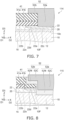
- FIG. 7 is a schematic cross-sectional view illustrating a part of a semiconductor device according to the first embodiment.
- the first region 22a may be provided between the first semiconductor region 10 and the first insulating portion 41a.
- FIG. 8 is a schematic cross-sectional view illustrating a part of a semiconductor device according to the first embodiment.
- the second electrode 52 includes a nitride region 52N and a conductive region 52C.
- a part of the nitride region 52N is provided between the second partial region 12 and the conductive region 52C.
- Another part of the nitride region 52N is provided between a part of the second insulating portion 41b and the second electrode portion 52b.
- the material of nitride region 52N is different from the material of conductive region 52C.
- the nitride region 52N includes gallium and nitrogen.
- the nitride region 52N is n-type GaN.
- the conductive region 52C is, for example, metal.
- a part of the second electrode 52 may include a semiconductor. For example, it becomes easier to obtain lower on-resistance.
- the semiconductor device 115 the first region 22a including fluorine is provided. Stable characteristics can be obtained.
- the configuration described with respect to the semiconductor devices 110 to 114 may be applied.
- FIG. 9 is a schematic cross-sectional view illustrating a semiconductor device according to the first embodiment.
- a semiconductor device 120 includes a second electrode conductive member 52P, the first insulating member 41, and a second insulating member 42.
- the configurations of the semiconductor devices 110 to 115 may be applied to the configurations excluding the second electrode conductive member 52P and the second insulating member 42.
- second electrode conductive member 52P is electrically connected to second electrode 52. At least a part of the first insulating member 41 is provided between the second semiconductor portion 22 and the second electrode portion 52b. At least a part of the second insulating member 42 is provided between the second electrode portion 52b and the second electrode conductive member 52P.
- the second electrode conductive member 52P functions, for example, as a field plate. The concentration of electric field is further relaxed.
- the first insulating member 41 includes silicon and nitrogen.
- the second insulating member 42 includes silicon and oxygen.
- the concentration of nitrogen in the second insulating member 42 is lower than the concentration of nitrogen in the first insulating member 41.
- the second insulating member 42 does not include nitrogen. With such a plurality of insulating members, more stable characteristics can be easily obtained.
- a first electrode conductive member 51P may be provided.
- the first electrode conductive member 51P is electrically connected to the first electrode 51.
- the first electrode conductive member 51P is electrically connected to the first electrode 51 at a position different from the cross section shown in FIG.9 .
- Another first electrode conductive member 51Q may be provided.
- the other first electrode conductive member 51Q is electrically connected to the first electrode 51.
- the second semiconductor portion 22 may include a region that overlaps the first electrode conductive member 51P.
- This region may include fluorine. Trap generation is further suppressed. This makes it easier to obtain stable characteristics.
- a third insulating member 43 may be provided on the second electrode conductive member 52P, the first electrode conductive member 51P, and the second insulating member.
- the third insulating member 43 may include, for example, silicon nitride.
- FIG. 10 is a schematic cross-sectional view illustrating a semiconductor device according to the first embodiment.
- the third electrode 53 is provided between the first semiconductor portion 21 and the second semiconductor portion 22 in the second direction D2.
- the third electrode 53 is, for example, a recessed gate electrode.
- a high threshold voltage can be obtained.
- the first region 22a including fluorine is provided. Stable characteristics can be obtained.
- a part of the first insulating portion 41a is provided between the first semiconductor portion 21 and at least a part of the third electrode 53 in the second direction D2. Another part of the first insulating portion 41a is provided between at least a part of the third electrode 53 and the second semiconductor portion 22 in the second direction D2.
- the second embodiment relates to a method for manufacturing a semiconductor device. Below, a method of manufacturing a portion including the second electrode 52 will be described.
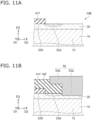
- FIGS. 11A and 11B are schematic cross-sectional views illustrating a method for manufacturing a semiconductor device according to the second embodiment.
- a structure body 10B is prepared.
- the structure body 10B includes the first semiconductor region 10 including Al x1 Ga 1-x1 N (0 ⁇ x1 ⁇ 1), the second semiconductor region 20 including Al x2 Ga 1-x2 N (0 ⁇ x2 ⁇ 1, x1 ⁇ x2), and a first insulating film 41f.
- the second semiconductor region 20 includes the first region 22a and the second region 22b.
- the second region 22b is located between the first semiconductor region 10 and the first insulating film 41f.
- the first region 22a is not covered with the first insulating film 41f.
- fluorine is introduced into the first region 22a.
- fluorine may be introduced by ion implantation using the first insulating film 41f as a mask.
- the concentration of fluorine in the first region 22a is higher than the concentration of fluorine in the second region 22b.
- the first region 22a includes fluorine and the second region 22b does not include fluorine.
- an electrode 50 is formed.
- the electrode 50 includes the first electrode portion 52a and the second electrode portion 52b.
- the first electrode portion 52a is electrically connected to a part of the first semiconductor region 10.
- the second electrode portion 52b is electrically connected to the first electrode portion 52a.
- the second electrode portion 52b overlaps the first region 22a in a direction from the first semiconductor region 10 to the second semiconductor region 20 (the third direction D3).
- the semiconductor device 110 is obtained. According to the embodiments, it is possible to provide a method of manufacturing a semiconductor device capable of improving characteristics.
- the electrode 50 corresponds to the second electrode 52.
- the first insulating film 41f corresponds to, for example, the first insulating portion 41a.
- the second insulating portion 41b may be formed before forming the electrode 50.
- FIGS. 12A and 12B are schematic cross-sectional views illustrating a method for manufacturing a semiconductor device according to the second embodiment.
- the structure body 10B is prepared in a method for manufacturing a semiconductor device according to the embodiment.
- the structure body 10B further includes a second insulating film 42f.
- the first insulating film 41f is provided between the second region 22b and a part of the second insulating film 42f.
- the first insulating film 41f is not provided between the first region 22a and the second insulating film 42f.
- the second insulating film 42f includes fluorine.
- fluorine is moved from the second insulating film 42f to the first region 22a.
- fluorine moves from the second insulating film 42f to the first region 22a by diffusion due to heat treatment or the like.
- the first region 22a including fluorine is obtained.
- the movement of fluorine is suppressed by the first insulating film 41f.
- the concentration of fluorine in the second region 22b is low.
- the second region 22b does not substantially include fluorine.
- introducing fluorine may include moving at least a part of the fluorine included in the second insulating film 42f to the first region 22a.
- the semiconductor device 110 can be obtained by such a manufacturing method.
- Information regarding length and thickness can be obtained by electron microscopy or the like.
- Information on the composition of materials can be obtained by SIMS (Secondary Ion Mass Spectrometry) or EDX (Energy dispersive X-ray spectroscopy).
- Embodiments may include the following configurations (e.g., technical proposals).
- a semiconductor device comprising:
- a concentration of fluorine in the first region is not less than 1 ⁇ 10 16 cm -3 and not more than 1 ⁇ 10 18 cm -3 .
- a method for manufacturing a semiconductor device comprising:
- a semiconductor device whose characteristics can be improved and a method for manufacturing the same are provided.
Landscapes
- Junction Field-Effect Transistors (AREA)
- Electrodes Of Semiconductors (AREA)
Applications Claiming Priority (1)
| Application Number | Priority Date | Filing Date | Title |
|---|---|---|---|
| JP2023083719A JP2024167557A (ja) | 2023-05-22 | 2023-05-22 | 半導体装置及びその製造方法 |
Publications (2)
| Publication Number | Publication Date |
|---|---|
| EP4468366A1 true EP4468366A1 (de) | 2024-11-27 |
| EP4468366B1 EP4468366B1 (de) | 2026-02-25 |
Family
ID=89843744
Family Applications (1)
| Application Number | Title | Priority Date | Filing Date |
|---|---|---|---|
| EP24155654.7A Active EP4468366B1 (de) | 2023-05-22 | 2024-02-20 | Halbleitervorrichtung und verfahren zu deren herstellung |
Country Status (4)
| Country | Link |
|---|---|
| US (1) | US20240395919A1 (de) |
| EP (1) | EP4468366B1 (de) |
| JP (1) | JP2024167557A (de) |
| CN (1) | CN119008657A (de) |
Citations (4)
| Publication number | Priority date | Publication date | Assignee | Title |
|---|---|---|---|---|
| US20110018002A1 (en) * | 2009-07-27 | 2011-01-27 | The Hong Kong University Of Science And Technology | Transistors and rectifiers utilizing hybrid electrodes and methods of fabricating the same |
| US20170033187A1 (en) * | 2015-07-31 | 2017-02-02 | Ohio State Innovation Foundation | Enhancement mode field effect transistor with doped buffer and drain field plate |
| US20200303533A1 (en) * | 2019-03-18 | 2020-09-24 | Cree, Inc. | Structures for Reducing Electron Concentration and Process for Reducing Electron Concentration |
| US20200335587A1 (en) * | 2019-04-19 | 2020-10-22 | Kabushiki Kaisha Toshiba | Semiconductor device |
-
2023
- 2023-05-22 JP JP2023083719A patent/JP2024167557A/ja active Pending
-
2024
- 2024-01-23 US US18/419,908 patent/US20240395919A1/en active Pending
- 2024-02-05 CN CN202410160038.9A patent/CN119008657A/zh active Pending
- 2024-02-20 EP EP24155654.7A patent/EP4468366B1/de active Active
Patent Citations (4)
| Publication number | Priority date | Publication date | Assignee | Title |
|---|---|---|---|---|
| US20110018002A1 (en) * | 2009-07-27 | 2011-01-27 | The Hong Kong University Of Science And Technology | Transistors and rectifiers utilizing hybrid electrodes and methods of fabricating the same |
| US20170033187A1 (en) * | 2015-07-31 | 2017-02-02 | Ohio State Innovation Foundation | Enhancement mode field effect transistor with doped buffer and drain field plate |
| US20200303533A1 (en) * | 2019-03-18 | 2020-09-24 | Cree, Inc. | Structures for Reducing Electron Concentration and Process for Reducing Electron Concentration |
| US20200335587A1 (en) * | 2019-04-19 | 2020-10-22 | Kabushiki Kaisha Toshiba | Semiconductor device |
Non-Patent Citations (1)
| Title |
|---|
| YANG CHAO ET AL: "High Breakdown Voltage and Low Dynamic ON-Resistance AlGaN/GaN HEMT with Fluorine Ion Implantation in SiNx Passivation Layer", vol. 14, no. 1, 1 December 2019 (2019-12-01), US, XP093204324, ISSN: 1931-7573, Retrieved from the Internet <URL:https://link.springer.com/content/pdf/10.1186/s11671-019-3025-8.pdf> DOI: 10.1186/s11671-019-3025-8 * |
Also Published As
| Publication number | Publication date |
|---|---|
| EP4468366B1 (de) | 2026-02-25 |
| CN119008657A (zh) | 2024-11-22 |
| JP2024167557A (ja) | 2024-12-04 |
| US20240395919A1 (en) | 2024-11-28 |
Similar Documents
| Publication | Publication Date | Title |
|---|---|---|
| US11404550B2 (en) | Semiconductor device and method for manufacturing the same | |
| US10600863B2 (en) | Semiconductor device and method for manufacturing the same | |
| US20250374586A1 (en) | Semiconductor device | |
| US11362219B2 (en) | Semiconductor device | |
| EP4468366A1 (de) | Halbleitervorrichtung und verfahren zu deren herstellung | |
| US11462637B2 (en) | Semiconductor device and manufacturing method for the same | |
| US20240154004A1 (en) | Nitride semiconductor and semiconductor device | |
| US20250203909A1 (en) | Semiconductor device | |
| US20250331217A1 (en) | Semiconductor device and method for manufacturing the same | |
| US20220384629A1 (en) | Semiconductor device | |
| US20250169148A1 (en) | Semiconductor device | |
| US11251293B2 (en) | Semiconductor device | |
| US20260096131A1 (en) | Semiconductor device | |
| US12538513B2 (en) | Semiconductor device and method for manufacturing the same | |
| US20260129896A1 (en) | Semiconductor device | |
| US20250275167A1 (en) | Semiconductor device and method for manufacturing the same | |
| US20250261420A1 (en) | Semiconductor device and manufacturing method for the same | |
| US20240047534A1 (en) | Semiconductor device | |
| US20260101561A1 (en) | Semiconductor device | |
| US20230253487A1 (en) | Semiconductor device | |
| US20260026062A1 (en) | Wafer, semiconductor device, and method for manufacturing wafer | |
| US20230187500A1 (en) | Semiconductor device | |
| US20230282708A1 (en) | Semiconductor device | |
| US20250056826A1 (en) | Semiconductor device | |
| US20250261421A1 (en) | Wafer and semiconductor device |
Legal Events
| Date | Code | Title | Description |
|---|---|---|---|
| PUAI | Public reference made under article 153(3) epc to a published international application that has entered the european phase |
Free format text: ORIGINAL CODE: 0009012 |
|
| STAA | Information on the status of an ep patent application or granted ep patent |
Free format text: STATUS: REQUEST FOR EXAMINATION WAS MADE |
|
| 17P | Request for examination filed |
Effective date: 20240205 |
|
| AK | Designated contracting states |
Kind code of ref document: A1 Designated state(s): AL AT BE BG CH CY CZ DE DK EE ES FI FR GB GR HR HU IE IS IT LI LT LU LV MC ME MK MT NL NO PL PT RO RS SE SI SK SM TR |
|
| REG | Reference to a national code |
Ref country code: DE Ref legal event code: R079 Free format text: PREVIOUS MAIN CLASS: H01L0029778000 Ipc: H10D0030470000 Ref country code: DE Ref legal event code: R079 Ref document number: 602024002715 Country of ref document: DE Free format text: PREVIOUS MAIN CLASS: H01L0029778000 Ipc: H10D0030470000 |
|
| GRAP | Despatch of communication of intention to grant a patent |
Free format text: ORIGINAL CODE: EPIDOSNIGR1 |
|
| STAA | Information on the status of an ep patent application or granted ep patent |
Free format text: STATUS: GRANT OF PATENT IS INTENDED |
|
| RIC1 | Information provided on ipc code assigned before grant |
Ipc: H10D 30/47 20250101AFI20250901BHEP Ipc: H10D 64/00 20250101ALI20250901BHEP Ipc: H10D 64/23 20250101ALI20250901BHEP Ipc: H10D 64/27 20250101ALI20250901BHEP Ipc: H10D 30/01 20250101ALN20250901BHEP Ipc: H10D 62/85 20250101ALN20250901BHEP |
|
| RIC1 | Information provided on ipc code assigned before grant |
Ipc: H10D 30/47 20250101AFI20250910BHEP Ipc: H10D 64/00 20250101ALI20250910BHEP Ipc: H10D 64/23 20250101ALI20250910BHEP Ipc: H10D 64/27 20250101ALI20250910BHEP Ipc: H10D 30/01 20250101ALN20250910BHEP Ipc: H10D 62/85 20250101ALN20250910BHEP |
|
| INTG | Intention to grant announced |
Effective date: 20250918 |
|
| GRAS | Grant fee paid |
Free format text: ORIGINAL CODE: EPIDOSNIGR3 |
|
| GRAJ | Information related to disapproval of communication of intention to grant by the applicant or resumption of examination proceedings by the epo deleted |
Free format text: ORIGINAL CODE: EPIDOSDIGR1 |
|
| GRAL | Information related to payment of fee for publishing/printing deleted |
Free format text: ORIGINAL CODE: EPIDOSDIGR3 |
|
| STAA | Information on the status of an ep patent application or granted ep patent |
Free format text: STATUS: REQUEST FOR EXAMINATION WAS MADE |
|
| GRAP | Despatch of communication of intention to grant a patent |
Free format text: ORIGINAL CODE: EPIDOSNIGR1 |
|
| STAA | Information on the status of an ep patent application or granted ep patent |
Free format text: STATUS: GRANT OF PATENT IS INTENDED |
|
| INTC | Intention to grant announced (deleted) | ||
| RIC1 | Information provided on ipc code assigned before grant |
Ipc: H10D 30/47 20250101AFI20251104BHEP Ipc: H10D 64/00 20250101ALI20251104BHEP Ipc: H10D 64/23 20250101ALI20251104BHEP Ipc: H10D 64/27 20250101ALI20251104BHEP Ipc: H10D 30/01 20250101ALN20251104BHEP Ipc: H10D 62/85 20250101ALN20251104BHEP |
|
| INTG | Intention to grant announced |
Effective date: 20251114 |
|
| RIC1 | Information provided on ipc code assigned before grant |
Ipc: H10D 30/47 20250101AFI20251110BHEP Ipc: H10D 64/00 20250101ALI20251110BHEP Ipc: H10D 64/23 20250101ALI20251110BHEP Ipc: H10D 64/27 20250101ALI20251110BHEP Ipc: H10D 30/01 20250101ALN20251110BHEP Ipc: H10D 62/85 20250101ALN20251110BHEP |
|
| GRAA | (expected) grant |
Free format text: ORIGINAL CODE: 0009210 |
|
| STAA | Information on the status of an ep patent application or granted ep patent |
Free format text: STATUS: THE PATENT HAS BEEN GRANTED |
|
| AK | Designated contracting states |
Kind code of ref document: B1 Designated state(s): AL AT BE BG CH CY CZ DE DK EE ES FI FR GB GR HR HU IE IS IT LI LT LU LV MC ME MK MT NL NO PL PT RO RS SE SI SK SM TR |
|
| REG | Reference to a national code |
Ref country code: CH Ref legal event code: F10 Free format text: ST27 STATUS EVENT CODE: U-0-0-F10-F00 (AS PROVIDED BY THE NATIONAL OFFICE) Effective date: 20260225 Ref country code: GB Ref legal event code: FG4D |
|
| REG | Reference to a national code |
Ref country code: DE Ref legal event code: R096 Ref document number: 602024002715 Country of ref document: DE |
|
| REG | Reference to a national code |
Ref country code: IE Ref legal event code: FG4D |