EP4467946A1 - Power device temperature estimation device for inverter - Google Patents
Power device temperature estimation device for inverter Download PDFInfo
- Publication number
- EP4467946A1 EP4467946A1 EP24175978.6A EP24175978A EP4467946A1 EP 4467946 A1 EP4467946 A1 EP 4467946A1 EP 24175978 A EP24175978 A EP 24175978A EP 4467946 A1 EP4467946 A1 EP 4467946A1
- Authority
- EP
- European Patent Office
- Prior art keywords
- temperature
- diode
- power device
- voltage
- inverter
- Prior art date
- Legal status (The legal status is an assumption and is not a legal conclusion. Google has not performed a legal analysis and makes no representation as to the accuracy of the status listed.)
- Granted
Links
Images


Classifications
-
- G—PHYSICS
- G01—MEASURING; TESTING
- G01K—MEASURING TEMPERATURE; MEASURING QUANTITY OF HEAT; THERMALLY-SENSITIVE ELEMENTS NOT OTHERWISE PROVIDED FOR
- G01K7/00—Measuring temperature based on the use of electric or magnetic elements directly sensitive to heat ; Power supply therefor, e.g. using thermoelectric elements
- G01K7/01—Measuring temperature based on the use of electric or magnetic elements directly sensitive to heat ; Power supply therefor, e.g. using thermoelectric elements using semiconducting elements having PN junctions
-
- H—ELECTRICITY
- H02—GENERATION; CONVERSION OR DISTRIBUTION OF ELECTRIC POWER
- H02P—CONTROL OR REGULATION OF ELECTRIC MOTORS, ELECTRIC GENERATORS OR DYNAMO-ELECTRIC CONVERTERS; CONTROLLING TRANSFORMERS, REACTORS OR CHOKE COILS
- H02P29/00—Arrangements for regulating or controlling electric motors, appropriate for both AC and DC motors
- H02P29/60—Controlling or determining the temperature of the motor or of the drive
- H02P29/68—Controlling or determining the temperature of the motor or of the drive based on the temperature of a drive component or a semiconductor component
-
- G—PHYSICS
- G01—MEASURING; TESTING
- G01K—MEASURING TEMPERATURE; MEASURING QUANTITY OF HEAT; THERMALLY-SENSITIVE ELEMENTS NOT OTHERWISE PROVIDED FOR
- G01K7/00—Measuring temperature based on the use of electric or magnetic elements directly sensitive to heat ; Power supply therefor, e.g. using thermoelectric elements
- G01K7/42—Circuits effecting compensation of thermal inertia; Circuits for predicting the stationary value of a temperature
-
- H—ELECTRICITY
- H02—GENERATION; CONVERSION OR DISTRIBUTION OF ELECTRIC POWER
- H02M—APPARATUS FOR CONVERSION BETWEEN AC AND AC, BETWEEN AC AND DC, OR BETWEEN DC AND DC, AND FOR USE WITH MAINS OR SIMILAR POWER SUPPLY SYSTEMS; CONVERSION OF DC OR AC INPUT POWER INTO SURGE OUTPUT POWER; CONTROL OR REGULATION THEREOF
- H02M1/00—Details of apparatus for conversion
- H02M1/32—Means for protecting converters other than automatic disconnection
- H02M1/327—Means for protecting converters other than automatic disconnection against abnormal temperatures
-
- H—ELECTRICITY
- H02—GENERATION; CONVERSION OR DISTRIBUTION OF ELECTRIC POWER
- H02M—APPARATUS FOR CONVERSION BETWEEN AC AND AC, BETWEEN AC AND DC, OR BETWEEN DC AND DC, AND FOR USE WITH MAINS OR SIMILAR POWER SUPPLY SYSTEMS; CONVERSION OF DC OR AC INPUT POWER INTO SURGE OUTPUT POWER; CONTROL OR REGULATION THEREOF
- H02M7/00—Conversion of AC power input into DC power output; Conversion of DC power input into AC power output
- H02M7/003—Constructional details, e.g. physical layout, assembly, wiring or busbar connections
-
- H—ELECTRICITY
- H02—GENERATION; CONVERSION OR DISTRIBUTION OF ELECTRIC POWER
- H02M—APPARATUS FOR CONVERSION BETWEEN AC AND AC, BETWEEN AC AND DC, OR BETWEEN DC AND DC, AND FOR USE WITH MAINS OR SIMILAR POWER SUPPLY SYSTEMS; CONVERSION OF DC OR AC INPUT POWER INTO SURGE OUTPUT POWER; CONTROL OR REGULATION THEREOF
- H02M7/00—Conversion of AC power input into DC power output; Conversion of DC power input into AC power output
- H02M7/42—Conversion of DC power input into AC power output without possibility of reversal
- H02M7/44—Conversion of DC power input into AC power output without possibility of reversal by static converters
- H02M7/48—Conversion of DC power input into AC power output without possibility of reversal by static converters using discharge tubes with control electrode or semiconductor devices with control electrode
- H02M7/53—Conversion of DC power input into AC power output without possibility of reversal by static converters using discharge tubes with control electrode or semiconductor devices with control electrode using devices of a triode or transistor type requiring continuous application of a control signal
- H02M7/537—Conversion of DC power input into AC power output without possibility of reversal by static converters using discharge tubes with control electrode or semiconductor devices with control electrode using devices of a triode or transistor type requiring continuous application of a control signal using semiconductor devices only, e.g. single switched pulse inverters
- H02M7/5387—Conversion of DC power input into AC power output without possibility of reversal by static converters using discharge tubes with control electrode or semiconductor devices with control electrode using devices of a triode or transistor type requiring continuous application of a control signal using semiconductor devices only, e.g. single switched pulse inverters in a bridge configuration
-
- H—ELECTRICITY
- H02—GENERATION; CONVERSION OR DISTRIBUTION OF ELECTRIC POWER
- H02M—APPARATUS FOR CONVERSION BETWEEN AC AND AC, BETWEEN AC AND DC, OR BETWEEN DC AND DC, AND FOR USE WITH MAINS OR SIMILAR POWER SUPPLY SYSTEMS; CONVERSION OF DC OR AC INPUT POWER INTO SURGE OUTPUT POWER; CONTROL OR REGULATION THEREOF
- H02M7/00—Conversion of AC power input into DC power output; Conversion of DC power input into AC power output
- H02M7/42—Conversion of DC power input into AC power output without possibility of reversal
- H02M7/44—Conversion of DC power input into AC power output without possibility of reversal by static converters
- H02M7/48—Conversion of DC power input into AC power output without possibility of reversal by static converters using discharge tubes with control electrode or semiconductor devices with control electrode
- H02M7/53—Conversion of DC power input into AC power output without possibility of reversal by static converters using discharge tubes with control electrode or semiconductor devices with control electrode using devices of a triode or transistor type requiring continuous application of a control signal
- H02M7/537—Conversion of DC power input into AC power output without possibility of reversal by static converters using discharge tubes with control electrode or semiconductor devices with control electrode using devices of a triode or transistor type requiring continuous application of a control signal using semiconductor devices only, e.g. single switched pulse inverters
- H02M7/5387—Conversion of DC power input into AC power output without possibility of reversal by static converters using discharge tubes with control electrode or semiconductor devices with control electrode using devices of a triode or transistor type requiring continuous application of a control signal using semiconductor devices only, e.g. single switched pulse inverters in a bridge configuration
- H02M7/53871—Conversion of DC power input into AC power output without possibility of reversal by static converters using discharge tubes with control electrode or semiconductor devices with control electrode using devices of a triode or transistor type requiring continuous application of a control signal using semiconductor devices only, e.g. single switched pulse inverters in a bridge configuration with automatic control of output voltage or current
-
- H—ELECTRICITY
- H02—GENERATION; CONVERSION OR DISTRIBUTION OF ELECTRIC POWER
- H02P—CONTROL OR REGULATION OF ELECTRIC MOTORS, ELECTRIC GENERATORS OR DYNAMO-ELECTRIC CONVERTERS; CONTROLLING TRANSFORMERS, REACTORS OR CHOKE COILS
- H02P29/00—Arrangements for regulating or controlling electric motors, appropriate for both AC and DC motors
- H02P29/02—Providing protection against overload without automatic interruption of supply
- H02P29/024—Detecting a fault condition, e.g. short circuit, locked rotor, open circuit or loss of load
-
- H—ELECTRICITY
- H05—ELECTRIC TECHNIQUES NOT OTHERWISE PROVIDED FOR
- H05K—PRINTED CIRCUITS; CASINGS OR CONSTRUCTIONAL DETAILS OF ELECTRIC APPARATUS; MANUFACTURE OF ASSEMBLAGES OF ELECTRICAL COMPONENTS
- H05K7/00—Constructional details common to different types of electric apparatus
- H05K7/20—Modifications to facilitate cooling, ventilating, or heating
- H05K7/20218—Modifications to facilitate cooling, ventilating, or heating using a liquid coolant without phase change in electronic enclosures
-
- H—ELECTRICITY
- H05—ELECTRIC TECHNIQUES NOT OTHERWISE PROVIDED FOR
- H05K—PRINTED CIRCUITS; CASINGS OR CONSTRUCTIONAL DETAILS OF ELECTRIC APPARATUS; MANUFACTURE OF ASSEMBLAGES OF ELECTRICAL COMPONENTS
- H05K7/00—Constructional details common to different types of electric apparatus
- H05K7/20—Modifications to facilitate cooling, ventilating, or heating
- H05K7/2089—Modifications to facilitate cooling, ventilating, or heating for power electronics, e.g. for inverters for controlling motor
- H05K7/209—Heat transfer by conduction from internal heat source to heat radiating structure
-
- G—PHYSICS
- G01—MEASURING; TESTING
- G01K—MEASURING TEMPERATURE; MEASURING QUANTITY OF HEAT; THERMALLY-SENSITIVE ELEMENTS NOT OTHERWISE PROVIDED FOR
- G01K2217/00—Temperature measurement using electric or magnetic components already present in the system to be measured
Definitions
- the present invention relates to a device that estimates a temperature of a power device provided in an inverter.
- a forward voltage at the time of a forward current of the freewheel diode being 1 A is detected by using a resistive voltage divider circuit including two resistors. Then, the temperature of the freewheel diode is determined on the basis of a relationship among the detected value, a current-voltage characteristic of the freewheel diode, and the temperature of the freewheel diode.
- a detection signal of the divided voltage value is output to a control section. Then, the control section determines the temperature of the freewheel diode.
- the voltage tolerated by the control section is only a few volts.
- the switching element, to which a high voltage of several hundred volts is applied as in an in-vehicle inverter, is the target, the voltage has to be divided at a level of 1/100.
- the present invention provides a device capable of estimating a temperature of a switching element, even in an inverter using a high voltage, with a high degree of accuracy.
- the present invention is defined in claim 1.
- the present invention relates to a power device temperature estimation device that is attached to an inverter and estimates a temperature of a power device using a temperature of a diode, particularly a freewheel diode (or a freewheeling diode, or a flyback diode), the inverter being installed with the power device that includes a switching element and the freewheel diode connected in anti-parallel with the switching element.
- the power device temperature estimation device includes: a voltage divider section having a voltage divider circuit that includes a first element and a second element connected in series with each other and is connected in parallel with the freewheel diode; a diode voltage detection section that is connected in parallel with the second element to detect a forward voltage of the freewheel diode on the basis of a divided voltage of the second element; a diode current detection section that detects a forward current of the freewheel diode; and a diode temperature estimation section that has characteristic data on a voltage, a current, and a temperature of the freewheel diode and estimates the temperature of the freewheel diode on the basis of the detected forward voltage, the detected forward current, and the characteristic data.
- the first element is a diode arranged in forward parallel with the freewheel diode
- the second element is a resistor.
- this power device temperature estimation device estimates the temperature of the switching element or the power device on the basis of the forward voltage of the freewheel diode.
- the forward voltage of the freewheel diode is detected using the resistive voltage divider circuit including the two resistors.
- the forward voltage of the freewheel diode is detected using the voltage divider circuit including the diode and the resistor.
- the resistor has a configuration equivalent to that the resistor is connected in parallel with the diode that is applied with the reduced forward voltage from the forward voltage of the freewheel diode by the forward voltage of the diode.
- a fluctuation amount itself of the forward voltage which is associated with a temperature change, can be detected without being divided.
- there is no need to detect a minute voltage change which facilitates estimation of the temperature and increases estimation accuracy thereof.
- the diode voltage detection section may have a transformer section that increases the divided voltage of the second element.
- an output side of the diode voltage detection section can be independent of (insulated from) a circuit in a high-voltage power system of several hundred volts. Even when electric power in the voltage divider section becomes abnormal, such abnormal electric power does not directly affect the diode voltage detection section.
- the diode voltage detection section may have a protection diode that is connected in parallel with the second element.
- the forward voltage of the freewheel diode is high.
- the diode (first element) in the voltage divider circuit fails and is short-circuited, the high voltage thereof is applied to the resistor (second element).
- the temperature estimation device may possibly be damaged.
- the protection diode the current can flow from a positive electrode side to a negative electrode side through the protection diode.
- the inverter may be further installed with: a board on which the power device is installed; and a heat dissipator attached to the board.
- the first element may separately be arranged from the board or may be arranged on the board in a contact state with the heat dissipator, and a temperature of the first element may thereby be maintained within an allowable range for detection of the forward voltage.
- the diode temperature estimation section may further have a dynamic thermal model to calculate the temperature of the power device, calculate an error between an estimated element temperature, which is the temperature of the power device estimated by the diode temperature estimation section, and a calculated element temperature, which is the temperature of the power device calculated using the dynamic thermal model, and Kalman gain, modify the dynamic thermal model by introducing the error and the Kalman gain, and adopt a calculated value using the modified dynamic thermal model as the temperature of the power device.
- a dynamic thermal model to calculate the temperature of the power device, calculate an error between an estimated element temperature, which is the temperature of the power device estimated by the diode temperature estimation section, and a calculated element temperature, which is the temperature of the power device calculated using the dynamic thermal model, and Kalman gain, modify the dynamic thermal model by introducing the error and the Kalman gain, and adopt a calculated value using the modified dynamic thermal model as the temperature of the power device.
- the temperature of the power device (the estimated element temperature) that is estimated by the diode temperature estimation section includes switching noise. Meanwhile, since the dynamic thermal model is not affected by switching, the calculated element temperature does not include the switching noise. Accordingly, by using a known Kalman filter method, the dynamic thermal model is modified by the error between these estimated element temperature and calculated element temperature and the Kalman gain. Then, the calculated value by the modified dynamic thermal model is adopted, or considered, or used as the temperature of the power device.
- the diode temperature estimation section can estimate the temperature of the power device with the reduced switching noise. As a result, estimation accuracy of the temperature of the power device is improved.
- the diode temperature estimation section further may have: a dynamic thermal model to calculate the temperature of the power device; and gain setting data on a specific output associated with noise of the inverter and a gain corresponding to the dynamic thermal model, calculate an error between an estimated element temperature, which is the temperature of the power device estimated by the diode temperature estimation section, and a calculated element temperature, which is the temperature of the power device calculated by the dynamic thermal model, acquire the gain from the gain setting data, modify the dynamic thermal model by introducing the error and the gain, and adopt a calculated value using the modified dynamic thermal model as the temperature of the power device.
- the calculation of the Kalman gain requires a large calculation load. This may cause a delay in responsiveness and an increase in a size of hardware. Meanwhile, when it is configured to predict a change in the switching noise in advance and thereby change the gain (so-called feed-forward control), the calculation of the Kalman gain becomes unnecessary. Thus, it is possible to ensure the high responsiveness by reducing the calculation load while improving the estimation accuracy of the temperature of the power device.
- the specific output may be a current value that is output from the inverter, and may be set in the gain setting data such that the gain is reduced as the current value is increased.
- the specific output may be a carrier frequency of the inverter, and may be set in the gain setting data such that the gain is reduced as the carrier frequency is reduced.
- the switching noise is increased as the current output from the inverter is increased.
- the switching noise is reduced as the current output from the inverter is reduced.
- the switching noise is increased as the carrier frequency of the inverter is reduced.
- the switching noise is reduced as the carrier frequency of the inverter is increased. That is, the current value output from the inverter and the carrier frequency of the inverter are each correlated with the change in the switching noise.
- the forward voltage of the freewheel diode may be detected in an off period of the switching element, and may be detected regardless of duration of the period.
- the influence of the noise can be suppressed by introducing the dynamic thermal model.
- the forward voltage can be detected regardless of the duration of the off period.
- detection timing of the forward voltage is no longer limited.
- the temperature of the power device can be estimated appropriately.
- a value that is acquired by averaging the plural forward voltages may be used to estimate the temperature of the freewheel diode, the plural forward voltages being detected within a predetermined electrical angle range, which is set in advance.
- the stable forward voltage can be acquired, and the temperature estimation accuracy is improved.
- the number of the forward voltages that can be detected at a predetermined electrical angle depends on the carrier frequency.
- the number of the detectable forward voltages is increased as the carrier frequency is increased.
- the switching noise is reduced as the carrier frequency is increased.
- the further stable forward voltage can be acquired.
- the temperature of the switching element can be estimated with the high degree of accuracy even in the inverter using the high voltage.
- the thermal damage of the inverter can effectively be prevented.
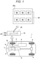
- Fig. 1 illustrates a preferred application example (a vehicle, particularly an electric vehicle 1) of the present invention.
- a motor particularly a drive motor 2
- the drive motor 2 may be a permanent magnet synchronous motor and is electrically connected to an inverter 10.
- the inverter 10 is connected to a drive battery 4 via a high-voltage wire 5.
- the inverter 10 is also connected to a controller 7 e.g., via a low-voltage wire 6 for control.
- the drive battery 4 includes plural lithium-ion batteries.
- a rated voltage of the drive battery 4 may be 300 V or higher, for example.
- the drive battery 4 supplies high-voltage direct current (DC) power to the inverter 10.
- the inverter 10 may be subjected to Pulse Width Modulation (PWM) control by the controller 7, the DC power thereof, particularly the direct current, is converted to alternating current (AC), e.g., three-phase alternating current (AC), and the three-phase AC is supplied to the drive motor 2.
- PWM Pulse Width Modulation
- AC alternating current
- AC three-phase alternating current
- the drive motor 2 thereby rotates.
- a transmission 8 may be coupled to a rear portion of the drive motor 2.
- a speed of rotary power that is output from the drive motor 2 may be changed by the transmission 8, and thereafter the changed rotary power or speed is transmitted to drive wheels 9 via a propeller shaft, a differential gear, and a pair of drive shafts. In this way, the electric vehicle 1 travels.
- a power module 20 including a board 20a and a heat dissipator 20b is installed in the inverter 10.
- a power device temperature estimation device 30 is further assembled to the power module 20 (this will be described below).
- One or more power devices e.g., six power devices 40 are installed on a surface of the board 20a.
- each of these power devices 40 includes a switching element 41 and a diode, particularly a freewheel diode (or a freewheeling diode, or a flyback diode) 42 connected in anti-parallel with this switching element 41.
- the board 20a may be provided with a known inverter circuit.
- the inverter circuit converts the DC power from the drive battery 4 to three-phase (U-phase, V-phase, and W-phase) AC power, and outputs the three-phase AC power to the drive motor 2, which rotates with the three-phase AC.
- the inverter circuit is provided with a positive electrode side wire 11 connected to a positive electrode side of the drive battery 4 and a negative electrode side wire 12 connected to a negative electrode side of the drive battery 4. Then, three circuits (half-bridge circuits 13) corresponding to the respective phases are connected in parallel between these positive electrode side wire 11 and negative electrode side wire 12.
- the two power devices 40, 40 may be connected in series to each of these half-bridge circuits 13, 13, 13.
- an output wire 14 for outputting the AC power to the drive motor 2 may be connected between these two power devices 40, 40.
- a smoothing capacitor 15 may be connected in parallel with these half-bridge circuits 13, 13, 13.
- each of the switching elements 41 is turned on/off at a high speed by the PWM control. This generates a current having a pseudo alternating waveform, and the current flows into the drive motor 2 via the output wire 14 in any of the phases. In addition, the current flows from the drive motor 2 to the negative electrode side wire 12 via the output wires 14 of the other phases.
- the freewheel diode 42 is provided to prevent damage to the switching element 41, which is caused by an instantaneous back electromotive force generated at the time when the respective switching element 41 is turned off.
- a voltage particularly a forward voltage
- a current particularly a forward current
- the switching element 41 which is turned on/off at the high speed and intermittently interrupts a large current, generates heat. Accordingly, in order to cool the power device 40, as illustrated in Fig. 1 , the heat dissipator 20b may be attached to a surface, particularly a back surface, of the board 20a.
- the heat dissipator 20b may be configured to be cooled by a refrigerant or a coolant that is circulated and supplied from a cooling system (not illustrated).
- the switching element 41 may be possibly damaged when the temperature thereof exceeds an upper limit temperature. For this reason, the temperature of the switching element 41 is detected, and control of the inverter 10 is thereby limited. However, since a heat generation amount of the switching element 41 is changed significantly according to a frequency of on/off, and the switching element 41 is always cooled while being actuated, the temperature of the switching element 41 is changed significantly in a short time. For this reason, high responsiveness is required to appropriately manage the temperature of the switching element 41 by detecting the temperature thereof with a high degree of accuracy.
- the power device 40 exemplified herein may be a metal-oxide-semiconductor field-effect transistor (MOSFET) or a reverse conducting IGBT (RC-IGBT) in which the switching element 41 and the freewheel diode 42 are integrated.
- MOSFET metal-oxide-semiconductor field-effect transistor
- RC-IGBT reverse conducting IGBT
- a temperature of the freewheel diode 42 can be taken as the temperature of the switching element 41.
- the switching element 41 and the freewheel diode 42 are configured as separate components.
- the switching element 41 and the freewheel diode 42 which constitute the same power device 40, may be arranged on the board 20a in close proximity to each other.
- the temperature of the freewheel diode 42 can be taken as the temperature of the switching element 41.
- the temperature of the freewheel diode 42 can be taken as the temperature of the switching element 41, which constitutes the same power device 40. It can be said that the temperatures of the freewheel diode 42 and the switching element 41 correspond to a temperature of the power device 40.
- the power device temperature estimation device 30 is attached to this inverter 10, and is devised to enable estimation of the temperature of the power device 40 with the high responsiveness and the high degree of accuracy on the basis of the forward voltage applied to the freewheel diode 42.
- the power device temperature estimation device 30 (also simply referred to as the "temperature estimation device 30") in this embodiment may be provided in the form of being independent of the board 20a. More specifically, the temperature estimation device 30 may be attached to the heat dissipator 20b while being externally attached to the board 20a. However, the temperature estimation device 30 may be partially integrated into the board 20a and thereby integrated with the board 20a.
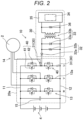
- the temperature estimation device 30 includes a diode current detection section 31, a voltage divider section 32, a diode voltage detection section 33, an AD converter 35, and the like.
- the voltage divider section 32 includes a voltage divider diode 32a (a first element), a voltage divider resistor 32b (a second element), and the like.
- the diode voltage detection section 33 includes a protection diode 33a, a transformer section 33b, and the like.
- This temperature estimation device 30 may set the single power device 40 as an estimation target. More specifically, the power device 40 that is arranged in a lower arm 13a of the U-phase may be set as the estimation target. In this case, when there is a difference in temperature among the power devices 40 due to a structure of the power module 20, the power device 40, the temperature of which is the highest, may be preferably set as the estimation target.
- the voltage divider section 32 and the like may be provided for each of the U, V, and W-phases or each of the power devices 40, and the plural power devices 40 may be set as the estimation targets.
- the structure becomes complicated, thermal damage of the inverter 10 can be prevented with the higher degree of accuracy.
- the diode current detection section 31 may be provided in a manner to correspond to the power device 40 as the estimation target, and detects the forward current flowing through the freewheel diode 42 therein. Any diode current detection section 31 that can measure a current value of a current detector, a current sensor, or the like may be employed.
- the diode current detection section 31 may be installed at a predetermined position in the wire on an upstream side or a downstream side of the power device 40 as the estimation target. Then, the diode current detection section 31 detects the current (the forward current) flowing through the freewheel diode 42 in an off period of the switching element 41.
- the voltage divider section 32 has a function to divide the high forward voltage of the freewheel diode 42 into two at a predetermined ratio. While being connected in series with each other, the voltage divider diode 32a (the first element) and the voltage divider resistor 32b (the second element) are connected in parallel with the freewheel diode 42 as the estimation target.
- the voltage divider diode 32a is arranged in parallel, particularly in forward parallel that is the same direction as the freewheel diode 42 (or the voltage divider diode 32a is arranged in parallel in the same direction as the freewheel diode 42). In other words, the voltage divider diode 32a is arranged in a direction of being anti-parallel to the switching element 41.
- the voltage divider diode 32a When compared using the same forward current, the voltage divider diode 32a, which is applied with the slightly lower forward voltage than that applied to the freewheel diode 42, is used.
- a size of the voltage divider resistor 32b may be selected according to a magnitude of the forward voltage applied to the voltage divider diode 32a.
- These voltage divider diode 32a and the voltage divider resistor 32b constitute a voltage divider circuit, and the forward voltage of the freewheel diode 42 is detected using this voltage divider circuit. That is, the diode voltage detection section 33 is connected in parallel with the voltage divider resistor 32b, and detects the forward voltage of the freewheel diode 42 on the basis of the divided voltage of the voltage divider resistor 32b.
- the resistor is also used for the first element (a resistive voltage divider circuit).
- the voltage has to be divided at a level of 1/100. Consequently, as described above, a fluctuation component associated with a temperature change in the forward voltage of the freewheel diode 42 as a detection target is also divided at the level of 1/100. As a result, it is required to detect a minute voltage change (for example, at a level of 100 ⁇ V), which makes it difficult to estimate the temperature with the high degree of accuracy.
- the voltage divider diode 32a is the first element.
- the voltage divider resistor 32b has a configuration equivalent to that the voltage divider resistor 32b is connected in parallel with a diode that is applied with the reduced forward voltage from the forward voltage of the freewheel diode 42 by the forward voltage of the voltage divider diode 32a.
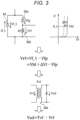
- a circuit configuration of the voltage divider section 32 is illustrated in a simplified manner at an upper left corner of Fig. 3 .
- a graph indicating a relationship between a forward voltage Vf and a forward current if of the diode is illustrated at an upper right corner of Fig. 3 .
- a solid line represents a forward voltage Vfd of the freewheel diode 42.
- a fluctuation amount of the forward voltage Vfd of the freewheel diode 42 is relatively small even when the forward current if is increased.
- a voltage fluctuation amount ⁇ Vf of the diode with respect to the temperature is almost the same and small even when a magnitude of the forward current differs.
- the fluctuation amount ⁇ Vf of the forward voltage Vf that is associated with the temperature increase is about -0.1 V even when the forward current thereof is changed to be increased or reduced.
- a forward current if_1 flows through the freewheel diode 42 and a forward voltage Vf_1 is applied thereto is assumed.
- the corresponding switching element 41 is turned off and thus can be ignored.
- a divided voltage Vrf of the voltage divider resistor 32b is Vf_1 - Vfp as expressed by an equation in Fig. 3 .
- the fluctuation amount ⁇ Vf itself of the forward voltage Vf, which is associated with the temperature change can be detected without being divided. As a result, there is no need to detect the minute voltage change, which facilitates the estimation of the temperature and increases estimation accuracy thereof.
- the voltage divider diode 32a is a resistive voltage divider circuit that includes a resistor with a resistance value R0, a fluctuation component by the temperature is (Rf/R0 + Rf) ⁇ ⁇ Vf. This pressure, which is reduced as a result of voltage dividing, has to be detected.
- the voltage divider diode 32a is separately arranged from the board 20a and is configured that an influence of the temperature change of the board 20a on the forward voltage of the voltage divider diode 32a can substantially be ignored (can be regarded that Vfp is substantially constant).
- the temperature divider diode 32a may be configured to arrange the voltage divider diode 32a in a contact state with the heat dissipator 20b such that the temperature thereof can be held within the above-described allowable range by heat radiation to the heat dissipator 20b.
- the forward voltage Vfp of the voltage divider diode 32a may be detected in consideration of the temperature change thereof. That is, a temperature sensor is installed in the voltage divider diode 32a and thereby actually measures the temperature of the voltage divider diodes 32a. Data on the temperature and a current-voltage characteristic (characteristic data) of the voltage divider diode 32a is stored in advance in a diode temperature estimation section 34. Then, based on the actually measured temperature of the voltage divider diode 32a and the characteristic data thereof, the forward voltage Vf of the voltage divider diode 32a, for which the temperature change is taken into consideration, is detected.
- the diode voltage detection section 33 may include the protection diode 33a, the transformer section 33b, and the like.
- the diode voltage detection section 33 has a function to output the divided voltage of the voltage divider resistor 32b e.g., as an analog signal of a predetermined magnitude in an insulated state from the circuit of the inverter 10.
- the protection diode 33a is connected in parallel with the voltage divider resistor 32b.
- the forward voltage of the freewheel diode 42 is high.
- the temperature estimation device 30 may possibly be damaged.
- the protection diode 33a as described above is provided. In this way, even when the voltage divider diode 32a is short-circuited, the current can flow from the positive electrode side to the negative electrode side through the protection diode 33a. Thus, it is possible to prevent application of the abnormally high voltage to the voltage divider resistor 32b. Consequently, it is possible to prevent the abnormally large current from flowing into the transformer section 33b. Therefore, the temperature estimation device 30 can be protected.
- the AD converter 35 may be connected to the voltage divider section 32 via the transformer section 33b.
- the AD converter 35 converts the analog signal of the voltage or the current, which is input from the transformer section 33b, to a digital signal.
- a load resistor 36 is connected in parallel between the AD converter 35 and the transformer section 33b.
- the transformer section 33b may include a known pulse transformer that is connected in parallel with the voltage divider resistor 32b, and the AD converter 35 is separated from the voltage divider section 32 by the transformer section 33b. In this way, the AD converter 35 can be independent of (insulated from) a circuit in a high-voltage power system of several hundred volts. Even when electric power in the voltage divider section 32 becomes abnormal, such abnormal electric power does not directly affect the AD converter 35.
- the protection diode 33a prevents the large current from flowing into the transformer section 33b. For this reason, the transformer section 33b does not have to be prepared for the large current, and thus can be downsized. Furthermore, only the relatively small current, which corresponds to the divided voltage of the voltage divider resistor 32b, may flow through the transformer section 33b. Thus, the transformer section 33b can increase the voltage to the appropriate voltage for the AD converter 35 with a relatively small turn number ratio.
- the primary-side voltage can be increased and output to the secondary side.
- the secondary-side voltage of transformer section 33b can fall within the range of about ⁇ 5 V.
- the divided voltage Vrf of the voltage divider resistor 32b and thus the forward voltage Vf of the freewheel diode 42 can stably be detected with the high degree of accuracy.
- the diode temperature estimation section 34 may include an IC chip and the like placed on a board of the AD converter 35. In other words, the diode temperature estimation section 34 may be provided as a functional structure in the AD converter 35.
- the diode temperature estimation section 34 may include: known hardware such as a processor and memory provided in the AD converter 35; and software such as a program installed in the memory and data.
- the diode temperature estimation section 34 cooperates with these types of the hardware and the software to estimate the temperature of the freewheel diode 42 by using the detected forward current if and forward voltage Vf.
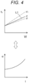
- the diode temperature estimation section 34 has characteristic data on the current, the voltage, and the temperature of the freewheel diode 42. More specifically, as indicated by a solid line L1 in an upper graph of Fig. 4 , the diode temperature estimation section 34 has voltage-temperature characteristic data that specifies a relationship between the forward voltage Vf of the freewheel diode 42 with respect to the forward current if as a reference and a temperature td thereof.
- the temperature td with respect to the forward voltage Vf may be increased accordingly.
- the forward current if is reduced (if-)
- the temperature td with respect to the forward voltage Vf is reduced accordingly.
- a magnitude of the change in the temperature td with respect to the forward voltage Vf, which is associated with a change in the forward current if, is increased with the increase in the forward current if.
- the diode temperature estimation section 34 may further have current correction data that is set on the basis of the above relationship and specifies a relationship between the forward current if and a correction coefficient ⁇ of the above-described voltage-temperature characteristic data, as indicated by a lower graph in Fig. 4 .
- the voltage-temperature characteristic data and the current correction data may be stored in the memory of the AD converter 35.
- the format of the characteristic data can be selected according to the specifications.
- voltage-temperature characteristic data for each current value may be used.
- the diode temperature estimation section 34 estimates the temperature td of the freewheel diode 42 on the basis of the forward current if of the freewheel diode 42 detected by the diode current detection section 31, the forward voltage Vf detected by the diode voltage detection section 33, and the characteristic data thereof.
- the correction value ⁇ is identified from the detected forward current if and the current correction data, and the voltage-temperature characteristic data is corrected to data that corresponds to the forward current if by using the correction value ⁇ .
- the temperature td of the freewheel diode 42 is identified from the detected forward voltage Vf and the corrected voltage-temperature characteristic data. As described above, the temperature td of the freewheel diode 42 corresponds to the temperature of the switching element 41 and also corresponds to the temperature of the power device 40.
- the forward current if and the forward voltage Vf described above are detected in a period in which the switching element 41 of the power device 40 as the estimation target is off (the off period). However, the switching element 41 is turned on/off at the high speed, and a length of the off period is changed. Thus, the detection of the forward current if and the forward voltage Vf is easily affected by noise that is generated by switching (switching noise).
- the detection of the forward current if and the forward voltage Vf may be more significantly affected by the switching noise as the off period is shortened. Accordingly, the influence of the switching noise can be reduced when the forward current if and the forward voltage Vf are detected in the long off period.
- extension of the off period possibly hinders appropriate driving of the drive motor 2.
- the temperature of the power device 40 cannot be estimated appropriately.
- the large switching noise may be superimposed on the forward current if and the forward voltage Vf that are detected in the short off period.
- the estimation accuracy of the temperature of the power device 40 is reduced.
- the temperature of the power device 40 that is estimated by the diode temperature estimation section 34 includes the switching noise, in order to estimate the temperature of the power device 40 with the high degree of accuracy, it is preferred to reduce the influence of the switching noise.
- this temperature estimation device 30 the estimation of the temperature of the power device 40, which is based on the detection of the forward voltage and the forward current of the freewheel diode 42 described above and the characteristic data of the freewheel diode 42, and the calculation of the temperature of the power device 40 using a dynamic thermal model are combined. In this way, the influence of the switching noise is reduced, and the estimation accuracy of the temperature of the power device 40 can be improved.
- Fig. 5 is a block diagram related to the estimation of the temperature of the power device 40.
- the diode temperature estimation section 34 may further include a dynamic thermal model 38.
- the diode temperature estimation section 34 may have extended software to estimate the temperature of the freewheel diode 42 by combining the dynamic thermal model 38 and the estimation of the temperature of the power device 40 described above. This extended software is based on the known Kalman filter.
- the dynamic thermal model 38 can be designed by using known thermo-fluid analysis software or the like on the basis of surrounding structures of the power device 40, such as the board 20a and the heat dissipator 20b, and the respective factors, such as the current and the voltage output from the inverter 10, that contribute to the temperature change in the power device 40.
- the current and the voltage may be constantly output to the drive motor 2.
- the refrigerant is circulated through the heat dissipator 20b.
- the temperature of the power device 40 is dynamically calculated by detecting and introducing each of the above factors that affect both of heat generation and heat dissipation of the power device 40.
- the dynamic thermal model 38 can be stored as a calculation program in the memory of the AD converter 35. Furthermore, a heat generation map and a heat dissipation map may be stored in the memory of the AD converter 35 and may appropriately be referred.
- the heat generation map may be set on the basis of a relationship between the heat generation amount of the power device 40 and each of the current and the voltage output from the inverter 10.
- the heat dissipation map may be set on the basis of a relationship between a heat dissipation amount of the power device 40 and each of a flow rate and a temperature of the refrigerant.
- the diode temperature estimation section 34 identifies the current and the voltage (the electric power), which are output from the inverter 10, from command values, actually measured values thereof, and the like. At the same time, the diode temperature estimation section 34 also identifies the flow rate and the temperature of the refrigerant, which is supplied to the heat dissipator 20b, from command values, actually measured values thereof, and the like. Then, each of these factors that affect both of the heat generation and the heat dissipation by the power device 40 is introduced into the dynamic thermal model 38. In this way, the temperature of the power device 40 is sequentially calculated.
- the diode temperature estimation section 34 may use known Kalman filter to calculate an error between the temperature of the power device 40 calculated using the dynamic thermal model 38 (the calculated element temperature) and the estimated element temperature and also calculate an optimal gain K (Kalman gain K) that minimizes the error. Then, the diode temperature estimation section 34 may introduce the calculated error and the Kalman gain K into the dynamic thermal model 38 to modify modification items related to the noise in the dynamic thermal model 38. In this way, the diode temperature estimation section 34 modifies the dynamic thermal model 38. Thereafter, the calculated value that is acquired by the modified dynamic thermal model 38 may be adopted or considered as the temperature of the power device 40.
- the dynamic thermal model 38 is successively modified, and the calculated element temperature converges to a true value.
- the diode temperature estimation section 34 can estimate the temperature of the power device 40 with the reduced switching noise. As a result, the estimation accuracy of the temperature of the power device 40 is improved.
- the calculated element temperature does not include the switching noise.
- the actually-measured estimated element temperature includes the switching noise. Accordingly, the error between these calculated element temperature and estimated element temperature may include a model error caused by the dynamic thermal model 38 and the noise error caused by the switching noise.
- the Kalman filter minimizes the model error while minimizing the noise error. More specifically, covariance of these errors is calculated, and the gain K that minimizes the covariance value is taken as the optimal gain K, that is, Kalman gain K.
- the calculation of the covariance is computationally burdensome. This may cause a delay in responsiveness.
- the hardware may excessively be increased in size, which prevents incorporation into the AD converter 35.
- the Kalman gain K may no longer be necessary, which reduces the calculation load and achieves the high responsiveness while improving the estimation accuracy of the temperature of the power device 40.
- the appropriate gain K is predicted on the basis of the current and the voltage output from the inverter 10, so as to change a magnitude of the gain K.
- the diode temperature estimation section 34 further includes predetermined gain setting data.
- the extended software described above is then configured to use this gain setting data.
- the gain setting data includes data on a correlation between the noise of the inverter 10, that is, specific output associated with the switching noise and the gain K corresponding to the dynamic thermal model 38 (also referred to as a predictive gain K to be distinguished from the Kalman gain K).
- the switching noise may be increased as the current output from the inverter 10 is increased.
- the switching noise is reduced as the current output from the inverter 10 is reduced.
- the current value that is output by the inverter 10 is correlated with the change in the switching noise (corresponding to the specific output).
- the diode temperature estimation section 34 may include the gain setting data (first gain setting data) on a correlation between a current value i output from the inverter 10 and the predictive gain K, as illustrated in Fig. 6 .
- the first gain setting data is set such that the predictive gain K is reduced as the current value i output from the inverter 10 is increased.
- the switching noise may be increased as a carrier frequency of the inverter 10 is reduced.
- the switching noise is reduced as the carrier frequency of the inverter 10 is increased.
- the carrier frequency of the inverter 10 is correlated with the change in the switching noise (corresponding to the specific output).
- the diode temperature estimation section 34 may include the gain setting data (second gain setting data) on a correlation between a carrier frequency fr of the inverter 10 and the predictive gain K, as illustrated in Fig. 7 .
- the second gain setting data is set such that the predictive gain K is reduced as the carrier frequency fr of the inverter 10 is reduced.
- the diode temperature estimation section 34 may also include the gain setting data (third gain setting data) on a correlation between the predictive gain K and each of the current value output from the inverter 10 and the carrier frequency of the inverter 10. This increases an amount of the data. However, the predictive gain K that corresponds to the changes in both of these specific outputs can be acquired.
- the diode temperature estimation section 34 predicts the appropriate gain K on the basis of the current value and the carrier frequency output from the inverter 10 and either one of the first gain setting data and the second gain setting data (or third gain setting data), and acquires the predictive gain K.
- the diode temperature estimation section 34 may acquire the predictive gain K that corresponds to the current value from the first gain setting data. Accordingly, when the current value that is output from the inverter 10 is reduced, the predictive gain K may be increased accordingly. When the current value that is output from the inverter 10 is increased, the predictive gain K is reduced accordingly.
- the diode temperature estimation section 34 may acquire the predictive gain K that corresponds to the carrier frequency from the second gain setting data. Accordingly, when the carrier frequency of the inverter 10 is increased, the predictive gain K is increased accordingly. When the carrier frequency of the inverter 10 is reduced, the predictive gain K is reduced accordingly.
- the diode temperature estimation section 34 may introduce the thus-acquired predictive gain K and the error between the estimated element temperature and the calculated element temperature into the dynamic thermal model 38, and may modify the modification items associated with the noise in the dynamic thermal model 38. In this way, the diode temperature estimation section 34 modifies the dynamic thermal model 38. Thereafter, the calculated value that is acquired by the modified dynamic thermal model 38 may be adopted, or considered, or used as the temperature of the power device 40.
- the dynamic thermal model 38 is successively modified, and the calculated element temperature converges to the true value.
- the diode temperature estimation section 34 can estimate the temperature of the power device 40 with the reduced switching noise.
- the estimation accuracy of the temperature of the power device 40 is improved.
- the calculation load can be reduced, and the high responsiveness can be ensured.
- the hardware can be downsized and can easily be integrated into the AD converter 35.
- Fig. 8 and Fig. 9 illustrate an example of temperature management control for the power device 40, for which the countermeasure against the noise is taken, by the temperature estimation device 30.
- This temperature estimation device 30 may take the countermeasure against the noise by the combination of the feed-forward control described above.
- the temperature estimation device 30 starts reading the relevant data such as the current output from the inverter 10 (step S1).
- the temperature estimation device 30 may always execute processing in the temperature management control while the inverter 10 is actuated, that is, while the electric power is applied to the onboard electrical equipment (Yes in step S2).
- the temperature estimation device 30 may stop the processing in the temperature management control when the inverter 10 is stopped (No in step S2).
- the temperature estimation device 30 may execute temperature estimation processing for the power device 40, which is based on the temperature of the freewheel diode 42, temperature calculation processing for the power device 40 using the dynamic thermal model 38, and acquisition processing of the predictive gain K in parallel. This enables the temperature estimation in a short time and thus ensures superior responsiveness.
- the temperature estimation device 30 may first execute processing to average the forward voltage Vf detected in a predetermined period (step S3). More specifically, the temperature estimation device 30 may average the plural forward voltages that are detected within a predetermined electrical angle range, which may be set in advance. The thus-acquired value (a VF average value) is used to estimate the temperature of the freewheel diode 42.
- Fig. 10 illustrates a timing chart related to on/off of each of the power devices 40 that are arranged in the lower arms 13a of the U, V, and W-phases.
- Each of hatched portions represents an on period, and a portion between two each of the hatched portions represents the off period.
- this temperature estimation device 30 sets the power device 40 of the U-phase as the estimation target.
- the forward voltage Vf in the off period (R1 or R2) thereof is detected.
- the detection of the forward voltage Vf may be more significantly affected by the switching noise as the off period is shortened. Accordingly, the influence of the switching noise can be reduced when the forward voltage Vf is detected in the long off period (for example, R2). However, when the forward voltage Vf is only detected in the long off period, the detection timing is significantly limited, which prevents the appropriate estimation of the temperature of the power device 40.
- the influence of the noise can be suppressed by the countermeasure against the noise described above.
- the forward voltage Vf can be detected regardless of duration of the off period.
- the forward voltage Vf can be detected even in the shortest off period R1.
- a predetermined period such as the electrical angle 120° (a period R3), may be set in advance, the forward voltage Vf is detected in each of the consecutive off periods within the range, and these forward voltages Vf are averaged. As a result, the stable forward voltage Vf can be acquired.
- the number of the forward voltages Vf that can be detected at the predetermined electrical angle depends on the carrier frequency. As the carrier frequency is increased, the number of the forward voltages Vf that can be detected is increased. As described above, the switching noise is reduced as the carrier frequency is increased. Thus, the further stable forward voltage Vf can be acquired.
- the temperature estimation device 30 may correct the characteristic data according to the detected forward current if (step S4). That is, as illustrated in Fig. 4 , the correction value ⁇ is identified from the detected forward current if and the current correction data, and the voltage-temperature characteristic data is corrected to the data that corresponds to the forward current if by using the correction value ⁇ .
- the temperature estimation device 30 estimates an element temperature Tsw on the basis of the acquired Vf average value and the corrected voltage-temperature characteristic data (step S5).
- the temperature estimation device 30 acquires the thus-estimated element temperature Tsw as an estimated element temperature Tsw1 (step S6).
- the temperature estimation device 30 may calculate the element temperature Tsw by using the dynamic thermal model 38 (step S7). More specifically, the temperature estimation device 30 may identify the current and the voltage (the electric power), which are output from the inverter 10, from the command values, the actually measured values thereof, and the like. At the same time, the temperature estimation device 30 may also identify the flow rate and the temperature of the refrigerant, which is supplied to the heat dissipator 20b, from the command values, the actually measured values thereof, and the like. Then, each of these factors that affect both of the heat generation and the heat dissipation by the power device 40 is introduced into the dynamic thermal model 38. In this way, the temperature estimation device 30 calculates the temperature of the power device 40.
- the temperature estimation device 30 calculates the temperature of the power device 40.
- the temperature estimation device 30 may acquire the thus-estimated element temperature Tsw as a calculated element temperature Tsw2 (step S8).
- the temperature estimation device 30 may subject the acquired estimated element temperature Tsw1 and calculated element temperature Tsw2 to subtraction processing, and thereby calculate errors thereof (step S9). Since only the subtraction is required, there is almost no calculation load.
- the temperature estimation device 30 may predictively acquire the gain K from the current and the voltage (the electric power) output from the inverter 10 on the basis of the specific outputs (the current value and the carrier frequency) associated with the noise (step S10).
- the diode temperature estimation section 34 may acquire the predictive gain K that corresponds to the current value from the first gain setting data.
- the diode temperature estimation section 34 mya acquire the predictive gain K that corresponds to the carrier frequency from the second gain setting data.
- the temperature estimation device 30 preferentially employs the predictive gain K that is based on either the current value or the carrier frequency, depending on the situation.
- the diode temperature estimation section 34 may acquire the predictive gain K that corresponds to the current value and the carrier frequency from the third gain setting data.
- the temperature estimation device 30 may introduce the calculated error and the acquired predictive gain K into the dynamic thermal model 38 (step S11).
- the temperature estimation device 30 modifies the dynamic thermal model 38 and estimates the element temperature Tsw by using the modified dynamic thermal model 38 (steps S12 and S13).
- the predictive gain K and the error may be used to modify the modification items associated with the noise of the dynamic thermal model 38.
- the dynamic thermal model 38 may be modified.
- the calculated value that is acquired by the modified dynamic thermal model 38 may be adopted, or considered, or used as the final estimated element temperature Tsw of the power device 40.
- the temperature estimation device 30 may determine whether the thus-estimated element temperature Tsw exceeds the predetermined temperature Ts (step S14). More specifically, the temperature estimation device 30 (the diode temperature estimation section 34) has preset data (current limit data) indicating a relationship between a maximum current value, which can be output from the inverter 10, and the element temperature Tsw, as illustrated in Fig. 11 .
- the temperature estimation device 30 may refer to the current limit data. If the estimated element temperature Tsw exceeds the temperature Ts (Yes in step S14), the temperature estimation device 30 may reduce the maximum current value, which can be output from the inverter 10 according to the element temperature Tsw, and may manage the current so as not to exceed such a value (step S15).
- the temperature estimation device 30 may refer to the current limit data, and, if the estimated element temperature Tsw does not exceed the temperature Ts (No in step S14), sets the maximum current value as usual (a constant value), and manages the current so as not to exceed such a value. Then, the processing returns to step S2, and the estimation processing of the element temperature Tsw is repeated.
- this temperature estimation device 30 can estimate the temperature of the switching element 41 with the high degree of accuracy even when the switching element 41 is provided in the inverter 10 using the high voltage. Therefore, the thermal damage of the inverter 10 can effectively be prevented by managing the temperature of the switching element 41 with this temperature estimation device 30.
- the present invention is not limited to the above-described embodiment and includes various configurations other than that described in the above-described embodiment.
- the description has been made on the application example to the electric vehicle 1.
- the present invention can also be applied to a hybrid vehicle.
Landscapes
- Engineering & Computer Science (AREA)
- Power Engineering (AREA)
- Physics & Mathematics (AREA)
- Microelectronics & Electronic Packaging (AREA)
- General Physics & Mathematics (AREA)
- Thermal Sciences (AREA)
- Inverter Devices (AREA)
- Power Conversion In General (AREA)
Abstract
Description
- The present invention relates to a device that estimates a temperature of a power device provided in an inverter.
- In recent years, electrification of automobiles has been advanced significantly. In conjunction with this trend, there is a tendency of increasing output of a drive motor mounted on the automobile and output of an inverter controlling the drive motor. When the output of the inverter is increased, a temperature of a power device including a switching element becomes high. In order to prevent thermal damage of the inverter caused by the above, it has been requested to detect a temperature of the switching element with a high degree of accuracy.
- For this purpose, it has been commonly practiced to attach a temperature sensor to a board, on which the power device is installed, and detect the temperature of the switching element. However, in this case, since the temperature sensor is remotely located from the power device, there are problems of a lack of responsiveness to detection and a significant detection error.
- Meanwhile, the following method has been proposed (for example, in Patent document 1). In the method, a temperature of a freewheel diode (or a freewheeling diode, or a flyback diode), which is connected in anti-parallel with the switching element, is detected, and such a temperature is taken as the temperature of the switching element.
- In detail, a forward voltage at the time of a forward current of the freewheel diode being 1 A is detected by using a resistive voltage divider circuit including two resistors. Then, the temperature of the freewheel diode is determined on the basis of a relationship among the detected value, a current-voltage characteristic of the freewheel diode, and the temperature of the freewheel diode.
- [Patent document 1]
JP2016-208770A - In the method disclosed in
Patent document 1, a detection signal of the divided voltage value is output to a control section. Then, the control section determines the temperature of the freewheel diode. In general, the voltage tolerated by the control section is only a few volts. Thus, when the switching element, to which a high voltage of several hundred volts is applied as in an in-vehicle inverter, is the target, the voltage has to be divided at a level of 1/100. - In this case, in the resistive voltage divider circuit described above, a fluctuation component by the temperature in the forward voltage of the freewheel diode as the detection target is also divided at the level of 1/100. As a result, it is required to detect a minute voltage change (for example, at a level of 100 µV), which makes it difficult to estimate the temperature with the high degree of accuracy.
- To handle the above problem, the present invention provides a device capable of estimating a temperature of a switching element, even in an inverter using a high voltage, with a high degree of accuracy.
- The present invention is defined in
claim 1. The present invention relates to a power device temperature estimation device that is attached to an inverter and estimates a temperature of a power device using a temperature of a diode, particularly a freewheel diode (or a freewheeling diode, or a flyback diode), the inverter being installed with the power device that includes a switching element and the freewheel diode connected in anti-parallel with the switching element. - The power device temperature estimation device includes: a voltage divider section having a voltage divider circuit that includes a first element and a second element connected in series with each other and is connected in parallel with the freewheel diode; a diode voltage detection section that is connected in parallel with the second element to detect a forward voltage of the freewheel diode on the basis of a divided voltage of the second element; a diode current detection section that detects a forward current of the freewheel diode; and a diode temperature estimation section that has characteristic data on a voltage, a current, and a temperature of the freewheel diode and estimates the temperature of the freewheel diode on the basis of the detected forward voltage, the detected forward current, and the characteristic data. The first element is a diode arranged in forward parallel with the freewheel diode, and the second element is a resistor.
- That is, similar to
Patent document 1, this power device temperature estimation device estimates the temperature of the switching element or the power device on the basis of the forward voltage of the freewheel diode. In the technique disclosed inPatent document 1, the forward voltage of the freewheel diode is detected using the resistive voltage divider circuit including the two resistors. Meanwhile, in this power device temperature estimation device, the forward voltage of the freewheel diode is detected using the voltage divider circuit including the diode and the resistor. - In a manner of speaking, the resistor has a configuration equivalent to that the resistor is connected in parallel with the diode that is applied with the reduced forward voltage from the forward voltage of the freewheel diode by the forward voltage of the diode. In other words, according to the voltage divider circuit with this configuration, a fluctuation amount itself of the forward voltage, which is associated with a temperature change, can be detected without being divided. As a result, there is no need to detect a minute voltage change, which facilitates estimation of the temperature and increases estimation accuracy thereof.
- The diode voltage detection section may have a transformer section that increases the divided voltage of the second element.
- In this way, an output side of the diode voltage detection section can be independent of (insulated from) a circuit in a high-voltage power system of several hundred volts. Even when electric power in the voltage divider section becomes abnormal, such abnormal electric power does not directly affect the diode voltage detection section.
- The diode voltage detection section may have a protection diode that is connected in parallel with the second element.
- The forward voltage of the freewheel diode is high. Thus, when the diode (first element) in the voltage divider circuit fails and is short-circuited, the high voltage thereof is applied to the resistor (second element). In such a case, the temperature estimation device may possibly be damaged. Meanwhile, with the protection diode, the current can flow from a positive electrode side to a negative electrode side through the protection diode. Thus, it is possible to prevent application of the abnormally high voltage. Consequently, it is possible to prevent the abnormally large current from flowing into the transformer section.
- The inverter may be further installed with: a board on which the power device is installed; and a heat dissipator attached to the board. The first element may separately be arranged from the board or may be arranged on the board in a contact state with the heat dissipator, and a temperature of the first element may thereby be maintained within an allowable range for detection of the forward voltage.
- In this way, an influence of the temperature change of the diode that constitutes the first element can be ignored. Thus, calculation of voltage dividing can be simplified.
- The diode temperature estimation section may further have a dynamic thermal model to calculate the temperature of the power device, calculate an error between an estimated element temperature, which is the temperature of the power device estimated by the diode temperature estimation section, and a calculated element temperature, which is the temperature of the power device calculated using the dynamic thermal model, and Kalman gain, modify the dynamic thermal model by introducing the error and the Kalman gain, and adopt a calculated value using the modified dynamic thermal model as the temperature of the power device.
- The temperature of the power device (the estimated element temperature) that is estimated by the diode temperature estimation section includes switching noise. Meanwhile, since the dynamic thermal model is not affected by switching, the calculated element temperature does not include the switching noise. Accordingly, by using a known Kalman filter method, the dynamic thermal model is modified by the error between these estimated element temperature and calculated element temperature and the Kalman gain. Then, the calculated value by the modified dynamic thermal model is adopted, or considered, or used as the temperature of the power device.
- As a result, the dynamic thermal model is successively modified, and the calculated element temperature converges to a true value. Thus, the diode temperature estimation section can estimate the temperature of the power device with the reduced switching noise. As a result, estimation accuracy of the temperature of the power device is improved.
- The diode temperature estimation section further may have: a dynamic thermal model to calculate the temperature of the power device; and gain setting data on a specific output associated with noise of the inverter and a gain corresponding to the dynamic thermal model, calculate an error between an estimated element temperature, which is the temperature of the power device estimated by the diode temperature estimation section, and a calculated element temperature, which is the temperature of the power device calculated by the dynamic thermal model, acquire the gain from the gain setting data, modify the dynamic thermal model by introducing the error and the gain, and adopt a calculated value using the modified dynamic thermal model as the temperature of the power device.
- The calculation of the Kalman gain requires a large calculation load. This may cause a delay in responsiveness and an increase in a size of hardware. Meanwhile, when it is configured to predict a change in the switching noise in advance and thereby change the gain (so-called feed-forward control), the calculation of the Kalman gain becomes unnecessary. Thus, it is possible to ensure the high responsiveness by reducing the calculation load while improving the estimation accuracy of the temperature of the power device.
- The specific output may be a current value that is output from the inverter, and may be set in the gain setting data such that the gain is reduced as the current value is increased. Alternatively, the specific output may be a carrier frequency of the inverter, and may be set in the gain setting data such that the gain is reduced as the carrier frequency is reduced.
- That is, the switching noise is increased as the current output from the inverter is increased. The switching noise is reduced as the current output from the inverter is reduced. In addition, the switching noise is increased as the carrier frequency of the inverter is reduced. The switching noise is reduced as the carrier frequency of the inverter is increased. That is, the current value output from the inverter and the carrier frequency of the inverter are each correlated with the change in the switching noise.
- Thus, when the gain is increased or reduced according to any of these changes, the appropriate gain can be acquired predictably.
- The forward voltage of the freewheel diode may be detected in an off period of the switching element, and may be detected regardless of duration of the period.
- The influence of the noise can be suppressed by introducing the dynamic thermal model. Thus, the forward voltage can be detected regardless of the duration of the off period. As a result, detection timing of the forward voltage is no longer limited. Thus, the temperature of the power device can be estimated appropriately.
- A value that is acquired by averaging the plural forward voltages may be used to estimate the temperature of the freewheel diode, the plural forward voltages being detected within a predetermined electrical angle range, which is set in advance.
- In this way, the stable forward voltage can be acquired, and the temperature estimation accuracy is improved. In addition, the number of the forward voltages that can be detected at a predetermined electrical angle depends on the carrier frequency. Thus, the number of the detectable forward voltages is increased as the carrier frequency is increased. As described above, the switching noise is reduced as the carrier frequency is increased. Thus, the further stable forward voltage can be acquired.
- According to the present invention, the temperature of the switching element can be estimated with the high degree of accuracy even in the inverter using the high voltage. Thus, the thermal damage of the inverter can effectively be prevented.
-
- [
Fig. 1] Fig. 1 is a schematic view illustrating an electric vehicle, to which the present invention is applied. - [
Fig. 2] Fig. 2 is a schematic view illustrating a configuration of a power device temperature estimation device. - [
Fig. 3] Fig. 3 is a schematic view illustrating detection of a forward voltage of a freewheel diode. - [
Fig. 4] Fig. 4 includes graphs schematically illustrating voltage-temperature characteristic data and current correction data. - [
Fig. 5] Fig. 5 is a block diagram related to estimation of a temperature of a power device. - [
Fig. 6] Fig. 6 is a conceptual graph of first gain setting data. - [
Fig. 7] Fig. 7 is a conceptual graph of second gain setting data. - [
Fig. 8] Fig. 8 is a flowchart related to temperature management control for the power device. - [
Fig. 9] Fig. 9 is a flowchart followingFig. 8 . - [
Fig. 10] Fig. 10 is schematic view illustrating a timing chart related to on/off of each of the power devices. - [
Fig. 11] Fig.11 is a conceptual view of current limit data. - A description will hereinafter be made on the present invention. However, the following description is essentially and merely illustrative.
-
Fig. 1 illustrates a preferred application example (a vehicle, particularly an electric vehicle 1) of the present invention. On theelectric vehicle 1, a motor, particularly adrive motor 2, is mounted as a drive source thereof. Thedrive motor 2 may be a permanent magnet synchronous motor and is electrically connected to aninverter 10. Theinverter 10 is connected to adrive battery 4 via a high-voltage wire 5. Theinverter 10 is also connected to acontroller 7 e.g., via a low-voltage wire 6 for control. - The
drive battery 4 includes plural lithium-ion batteries. A rated voltage of thedrive battery 4 may be 300 V or higher, for example. Thedrive battery 4 supplies high-voltage direct current (DC) power to theinverter 10. Theinverter 10 may be subjected to Pulse Width Modulation (PWM) control by thecontroller 7, the DC power thereof, particularly the direct current, is converted to alternating current (AC), e.g., three-phase alternating current (AC), and the three-phase AC is supplied to thedrive motor 2. Thedrive motor 2 thereby rotates. - A
transmission 8 may be coupled to a rear portion of thedrive motor 2. A speed of rotary power that is output from thedrive motor 2 may be changed by thetransmission 8, and thereafter the changed rotary power or speed is transmitted to drivewheels 9 via a propeller shaft, a differential gear, and a pair of drive shafts. In this way, theelectric vehicle 1 travels. - As illustrated in a simplified manner in
Fig. 1 , apower module 20 including aboard 20a and aheat dissipator 20b is installed in theinverter 10. A power devicetemperature estimation device 30 is further assembled to the power module 20 (this will be described below). One or more power devices, e.g., sixpower devices 40 are installed on a surface of theboard 20a. As illustrated inFig. 2 , each of thesepower devices 40 includes a switchingelement 41 and a diode, particularly a freewheel diode (or a freewheeling diode, or a flyback diode) 42 connected in anti-parallel with this switchingelement 41. - The
board 20a may be provided with a known inverter circuit. The inverter circuit converts the DC power from thedrive battery 4 to three-phase (U-phase, V-phase, and W-phase) AC power, and outputs the three-phase AC power to thedrive motor 2, which rotates with the three-phase AC. The inverter circuit is provided with a positiveelectrode side wire 11 connected to a positive electrode side of thedrive battery 4 and a negativeelectrode side wire 12 connected to a negative electrode side of thedrive battery 4. Then, three circuits (half-bridge circuits 13) corresponding to the respective phases are connected in parallel between these positiveelectrode side wire 11 and negativeelectrode side wire 12. - The two
power devices bridge circuits output wire 14 for outputting the AC power to thedrive motor 2 may be connected between these twopower devices electrode side wire 11 and the negativeelectrode side wire 12 on an input side from these half-bridge circuits capacitor 15 may be connected in parallel with these half-bridge circuits - When the
inverter 10 is actuated, each of the switchingelements 41 is turned on/off at a high speed by the PWM control. This generates a current having a pseudo alternating waveform, and the current flows into thedrive motor 2 via theoutput wire 14 in any of the phases. In addition, the current flows from thedrive motor 2 to the negativeelectrode side wire 12 via theoutput wires 14 of the other phases. - The
freewheel diode 42 is provided to prevent damage to the switchingelement 41, which is caused by an instantaneous back electromotive force generated at the time when therespective switching element 41 is turned off. Thus, when therespective switching element 41 is turned off, a voltage (particularly a forward voltage) is applied to and a current (particularly a forward current) flows through thefreewheel diode 42. - The switching
element 41, which is turned on/off at the high speed and intermittently interrupts a large current, generates heat. Accordingly, in order to cool thepower device 40, as illustrated inFig. 1 , theheat dissipator 20b may be attached to a surface, particularly a back surface, of theboard 20a. Theheat dissipator 20b may be configured to be cooled by a refrigerant or a coolant that is circulated and supplied from a cooling system (not illustrated). - The switching
element 41 may be possibly damaged when the temperature thereof exceeds an upper limit temperature. For this reason, the temperature of the switchingelement 41 is detected, and control of theinverter 10 is thereby limited. However, since a heat generation amount of the switchingelement 41 is changed significantly according to a frequency of on/off, and the switchingelement 41 is always cooled while being actuated, the temperature of the switchingelement 41 is changed significantly in a short time. For this reason, high responsiveness is required to appropriately manage the temperature of the switchingelement 41 by detecting the temperature thereof with a high degree of accuracy. - The
power device 40 exemplified herein may be a metal-oxide-semiconductor field-effect transistor (MOSFET) or a reverse conducting IGBT (RC-IGBT) in which theswitching element 41 and thefreewheel diode 42 are integrated. Thus, a temperature of thefreewheel diode 42 can be taken as the temperature of the switchingelement 41. - There is a type of the
power device 40 in which theswitching element 41 and thefreewheel diode 42 are configured as separate components. Also, in this case, the switchingelement 41 and thefreewheel diode 42, which constitute thesame power device 40, may be arranged on theboard 20a in close proximity to each other. Thus, also, in this case, the temperature of thefreewheel diode 42 can be taken as the temperature of the switchingelement 41. - In other words, the temperature of the
freewheel diode 42 can be taken as the temperature of the switchingelement 41, which constitutes thesame power device 40. It can be said that the temperatures of thefreewheel diode 42 and the switchingelement 41 correspond to a temperature of thepower device 40. For this reason, the power devicetemperature estimation device 30 is attached to thisinverter 10, and is devised to enable estimation of the temperature of thepower device 40 with the high responsiveness and the high degree of accuracy on the basis of the forward voltage applied to thefreewheel diode 42. - As illustrated in
Fig. 1 , in thepower module 20, the power device temperature estimation device 30 (also simply referred to as the "temperature estimation device 30") in this embodiment may be provided in the form of being independent of theboard 20a. More specifically, thetemperature estimation device 30 may be attached to theheat dissipator 20b while being externally attached to theboard 20a. However, thetemperature estimation device 30 may be partially integrated into theboard 20a and thereby integrated with theboard 20a. - As illustrated in
Fig. 2 , thetemperature estimation device 30 includes a diodecurrent detection section 31, avoltage divider section 32, a diodevoltage detection section 33, anAD converter 35, and the like. Thevoltage divider section 32 includes avoltage divider diode 32a (a first element), avoltage divider resistor 32b (a second element), and the like. The diodevoltage detection section 33 includes aprotection diode 33a, atransformer section 33b, and the like. - This
temperature estimation device 30 may set thesingle power device 40 as an estimation target. More specifically, thepower device 40 that is arranged in alower arm 13a of the U-phase may be set as the estimation target. In this case, when there is a difference in temperature among thepower devices 40 due to a structure of thepower module 20, thepower device 40, the temperature of which is the highest, may be preferably set as the estimation target. - Alternatively, the
voltage divider section 32 and the like may be provided for each of the U, V, and W-phases or each of thepower devices 40, and theplural power devices 40 may be set as the estimation targets. In this case, although the structure becomes complicated, thermal damage of theinverter 10 can be prevented with the higher degree of accuracy. - The diode
current detection section 31 may be provided in a manner to correspond to thepower device 40 as the estimation target, and detects the forward current flowing through thefreewheel diode 42 therein. Any diodecurrent detection section 31 that can measure a current value of a current detector, a current sensor, or the like may be employed. - For example, as illustrated in
Fig. 2 , the diodecurrent detection section 31 may be installed at a predetermined position in the wire on an upstream side or a downstream side of thepower device 40 as the estimation target. Then, the diodecurrent detection section 31 detects the current (the forward current) flowing through thefreewheel diode 42 in an off period of the switchingelement 41. - The
voltage divider section 32 has a function to divide the high forward voltage of thefreewheel diode 42 into two at a predetermined ratio. While being connected in series with each other, thevoltage divider diode 32a (the first element) and thevoltage divider resistor 32b (the second element) are connected in parallel with thefreewheel diode 42 as the estimation target. Thevoltage divider diode 32a is arranged in parallel, particularly in forward parallel that is the same direction as the freewheel diode 42 (or thevoltage divider diode 32a is arranged in parallel in the same direction as the freewheel diode 42). In other words, thevoltage divider diode 32a is arranged in a direction of being anti-parallel to the switchingelement 41. - When compared using the same forward current, the
voltage divider diode 32a, which is applied with the slightly lower forward voltage than that applied to thefreewheel diode 42, is used. A size of thevoltage divider resistor 32b may be selected according to a magnitude of the forward voltage applied to thevoltage divider diode 32a. - These
voltage divider diode 32a and thevoltage divider resistor 32b constitute a voltage divider circuit, and the forward voltage of thefreewheel diode 42 is detected using this voltage divider circuit. That is, the diodevoltage detection section 33 is connected in parallel with thevoltage divider resistor 32b, and detects the forward voltage of thefreewheel diode 42 on the basis of the divided voltage of thevoltage divider resistor 32b. - In the conventional voltage divider circuit, the resistor is also used for the first element (a resistive voltage divider circuit). However, in such a case, when a high voltage of several hundred volts or the like is applied to the switching
element 41 as the target, the voltage has to be divided at a level of 1/100. Consequently, as described above, a fluctuation component associated with a temperature change in the forward voltage of thefreewheel diode 42 as a detection target is also divided at the level of 1/100. As a result, it is required to detect a minute voltage change (for example, at a level of 100 µV), which makes it difficult to estimate the temperature with the high degree of accuracy. - Meanwhile, in this
voltage divider section 32, thevoltage divider diode 32a is the first element. In a manner of speaking, thevoltage divider resistor 32b has a configuration equivalent to that thevoltage divider resistor 32b is connected in parallel with a diode that is applied with the reduced forward voltage from the forward voltage of thefreewheel diode 42 by the forward voltage of thevoltage divider diode 32a. - A circuit configuration of the
voltage divider section 32 is illustrated in a simplified manner at an upper left corner ofFig. 3 . A graph indicating a relationship between a forward voltage Vf and a forward current if of the diode is illustrated at an upper right corner ofFig. 3 . A solid line represents a forward voltage Vfd of thefreewheel diode 42. A fluctuation amount of the forward voltage Vfd of thefreewheel diode 42 is relatively small even when the forward current if is increased. - When the temperature of the
freewheel diode 42 is increased, the forward voltage Vfd thereof is shifted in a reduction direction according to an increase amount of the temperature as indicated by an imaginary line, and is reduced (ΔVf). - Unlike the resistor, a voltage fluctuation amount ΔVf of the diode with respect to the temperature is almost the same and small even when a magnitude of the forward current differs. For example, in a case of the
power device 40, the fluctuation amount ΔVf of the forward voltage Vf that is associated with the temperature increase is about -0.1 V even when the forward current thereof is changed to be increased or reduced. - As illustrated in
Fig. 3 , a case where a forward current if_1 flows through thefreewheel diode 42 and a forward voltage Vf_1 is applied thereto is assumed. Thecorresponding switching element 41 is turned off and thus can be ignored. In such a case, a divided voltage Vrf of thevoltage divider resistor 32b is Vf_1 - Vfp as expressed by an equation inFig. 3 . When the temperature change is reflected thereto, Vdf + ΔVf - Vfp. - In other words, according to the voltage divider circuit with this configuration, the fluctuation amount ΔVf itself of the forward voltage Vf, which is associated with the temperature change, can be detected without being divided. As a result, there is no need to detect the minute voltage change, which facilitates the estimation of the temperature and increases estimation accuracy thereof.
- By the way, in the case where the
voltage divider diode 32a is a resistive voltage divider circuit that includes a resistor with a resistance value R0, a fluctuation component by the temperature is (Rf/R0 + Rf) · ΔVf. This pressure, which is reduced as a result of voltage dividing, has to be detected. - Here, the
voltage divider diode 32a is separately arranged from theboard 20a and is configured that an influence of the temperature change of theboard 20a on the forward voltage of thevoltage divider diode 32a can substantially be ignored (can be regarded that Vfp is substantially constant). - That is, even when a temperature of the
voltage divider diode 32a is changed, the temperature is held within an allowable range for the detection of the forward voltage Vf_1 of thefreewheel diode 42. In the case where thevoltage divider diode 32a is arranged on theboard 20a, it may be configured to arrange thevoltage divider diode 32a in a contact state with theheat dissipator 20b such that the temperature thereof can be held within the above-described allowable range by heat radiation to theheat dissipator 20b. - In this way, an influence of the temperature change of the
voltage divider diode 32a can be ignored. Thus, the calculation of voltage dividing can be simplified. - The forward voltage Vfp of the
voltage divider diode 32a may be detected in consideration of the temperature change thereof. That is, a temperature sensor is installed in thevoltage divider diode 32a and thereby actually measures the temperature of thevoltage divider diodes 32a. Data on the temperature and a current-voltage characteristic (characteristic data) of thevoltage divider diode 32a is stored in advance in a diodetemperature estimation section 34. Then, based on the actually measured temperature of thevoltage divider diode 32a and the characteristic data thereof, the forward voltage Vf of thevoltage divider diode 32a, for which the temperature change is taken into consideration, is detected. - As described above, the diode
voltage detection section 33 may include theprotection diode 33a, thetransformer section 33b, and the like. The diodevoltage detection section 33 has a function to output the divided voltage of thevoltage divider resistor 32b e.g., as an analog signal of a predetermined magnitude in an insulated state from the circuit of theinverter 10. - In a state of being arranged oppositely from the
freewheel diode 42 and thevoltage divider diode 32a, theprotection diode 33a is connected in parallel with thevoltage divider resistor 32b. The forward voltage of thefreewheel diode 42 is high. Thus, when thevoltage divider diode 32a fails and is short-circuited, the high voltage is applied to thevoltage divider resistor 32b. In such a case, thetemperature estimation device 30 may possibly be damaged. - To handle such a problem, the
protection diode 33a as described above is provided. In this way, even when thevoltage divider diode 32a is short-circuited, the current can flow from the positive electrode side to the negative electrode side through theprotection diode 33a. Thus, it is possible to prevent application of the abnormally high voltage to thevoltage divider resistor 32b. Consequently, it is possible to prevent the abnormally large current from flowing into thetransformer section 33b. Therefore, thetemperature estimation device 30 can be protected. - The
AD converter 35 may be connected to thevoltage divider section 32 via thetransformer section 33b. TheAD converter 35 converts the analog signal of the voltage or the current, which is input from thetransformer section 33b, to a digital signal. Aload resistor 36 is connected in parallel between theAD converter 35 and thetransformer section 33b. - The
transformer section 33b may include a known pulse transformer that is connected in parallel with thevoltage divider resistor 32b, and theAD converter 35 is separated from thevoltage divider section 32 by thetransformer section 33b. In this way, theAD converter 35 can be independent of (insulated from) a circuit in a high-voltage power system of several hundred volts. Even when electric power in thevoltage divider section 32 becomes abnormal, such abnormal electric power does not directly affect theAD converter 35. - In addition, the
protection diode 33a prevents the large current from flowing into thetransformer section 33b. For this reason, thetransformer section 33b does not have to be prepared for the large current, and thus can be downsized. Furthermore, only the relatively small current, which corresponds to the divided voltage of thevoltage divider resistor 32b, may flow through thetransformer section 33b. Thus, thetransformer section 33b can increase the voltage to the appropriate voltage for theAD converter 35 with a relatively small turn number ratio. - More specifically, in general, a tolerable voltage by the
AD Converter 35 may be about ±5 V. Accordingly, a secondary-side voltage Vad of thetransformer section 33b has to fall within such a range. Meanwhile, as indicated by the drawing and an equation in a lower portion ofFig. 3 , thetransformer section 33b converts a primary-side voltage (that is, the divided voltage Vrf of thevoltage divider resistor 32b) according to a ratio between a primary-side turn number (T1) of thetransformer section 33b connected in parallel with thevoltage divider resistor 32b and a secondary-side turn number (T2) of thetransformer section 33b connected to the AD converter 35 (a turn number ratio Tvf: T2/T1). Then, thetransformer section 33b outputs the converted primary-side voltage to the secondary side (Vad = Tvf . Vrf) . - Since the current flowing through the primary side of the
transformer section 33b is relatively small, by setting the turn number ratio Tvf to be increased by several times (for example, four times), the primary-side voltage can be increased and output to the secondary side. In this way, the secondary-side voltage oftransformer section 33b can fall within the range of about ±5 V. As a result, the divided voltage Vrf of thevoltage divider resistor 32b and thus the forward voltage Vf of thefreewheel diode 42 can stably be detected with the high degree of accuracy. - The diode
temperature estimation section 34 may include an IC chip and the like placed on a board of theAD converter 35. In other words, the diodetemperature estimation section 34 may be provided as a functional structure in theAD converter 35. - More specifically, the diode
temperature estimation section 34 may include: known hardware such as a processor and memory provided in theAD converter 35; and software such as a program installed in the memory and data. The diodetemperature estimation section 34 cooperates with these types of the hardware and the software to estimate the temperature of thefreewheel diode 42 by using the detected forward current if and forward voltage Vf. - In other words, the diode
temperature estimation section 34 has characteristic data on the current, the voltage, and the temperature of thefreewheel diode 42. More specifically, as indicated by a solid line L1 in an upper graph ofFig. 4 , the diodetemperature estimation section 34 has voltage-temperature characteristic data that specifies a relationship between the forward voltage Vf of thefreewheel diode 42 with respect to the forward current if as a reference and a temperature td thereof. - Although the relationship between the forward voltage Vf of the
freewheel diode 42 and the temperature td thereof may be relatively small, this relationship is changed according to a magnitude of the forward current if (see the upper right graph inFig. 3 ). - For example, as indicated by a virtual line in the upper graph of
Fig. 4 , when the forward current if is increased (if+), the temperature td with respect to the forward voltage Vf may be increased accordingly. When the forward current if is reduced (if-), the temperature td with respect to the forward voltage Vf is reduced accordingly. A magnitude of the change in the temperature td with respect to the forward voltage Vf, which is associated with a change in the forward current if, is increased with the increase in the forward current if. - For this reason, the diode
temperature estimation section 34 may further have current correction data that is set on the basis of the above relationship and specifies a relationship between the forward current if and a correction coefficient α of the above-described voltage-temperature characteristic data, as indicated by a lower graph inFig. 4 . - The voltage-temperature characteristic data and the current correction data may be stored in the memory of the
AD converter 35. The format of the characteristic data can be selected according to the specifications. Instead of the current correction data, voltage-temperature characteristic data for each current value may be used. - The diode
temperature estimation section 34 estimates the temperature td of thefreewheel diode 42 on the basis of the forward current if of thefreewheel diode 42 detected by the diodecurrent detection section 31, the forward voltage Vf detected by the diodevoltage detection section 33, and the characteristic data thereof. - More specifically, the correction value α is identified from the detected forward current if and the current correction data, and the voltage-temperature characteristic data is corrected to data that corresponds to the forward current if by using the correction value α. Then, the temperature td of the
freewheel diode 42 is identified from the detected forward voltage Vf and the corrected voltage-temperature characteristic data. As described above, the temperature td of thefreewheel diode 42 corresponds to the temperature of the switchingelement 41 and also corresponds to the temperature of thepower device 40. - The forward current if and the forward voltage Vf described above are detected in a period in which the
switching element 41 of thepower device 40 as the estimation target is off (the off period). However, the switchingelement 41 is turned on/off at the high speed, and a length of the off period is changed. Thus, the detection of the forward current if and the forward voltage Vf is easily affected by noise that is generated by switching (switching noise). - For example, the detection of the forward current if and the forward voltage Vf may be more significantly affected by the switching noise as the off period is shortened. Accordingly, the influence of the switching noise can be reduced when the forward current if and the forward voltage Vf are detected in the long off period. However, extension of the off period possibly hinders appropriate driving of the
drive motor 2. In addition, when the detection of the forward current if and the forward voltage Vf is limited in the long off period, the temperature of thepower device 40 cannot be estimated appropriately. - Meanwhile, the large switching noise may be superimposed on the forward current if and the forward voltage Vf that are detected in the short off period. As a result, the estimation accuracy of the temperature of the
power device 40 is reduced. In other words, since the temperature of thepower device 40 that is estimated by the diode temperature estimation section 34 (an estimated element temperature) includes the switching noise, in order to estimate the temperature of thepower device 40 with the high degree of accuracy, it is preferred to reduce the influence of the switching noise. - Accordingly, in this
temperature estimation device 30, the estimation of the temperature of thepower device 40, which is based on the detection of the forward voltage and the forward current of thefreewheel diode 42 described above and the characteristic data of thefreewheel diode 42, and the calculation of the temperature of thepower device 40 using a dynamic thermal model are combined. In this way, the influence of the switching noise is reduced, and the estimation accuracy of the temperature of thepower device 40 can be improved. -
Fig. 5 is a block diagram related to the estimation of the temperature of thepower device 40. The diodetemperature estimation section 34 may further include a dynamicthermal model 38. In addition, the diodetemperature estimation section 34 may have extended software to estimate the temperature of thefreewheel diode 42 by combining the dynamicthermal model 38 and the estimation of the temperature of thepower device 40 described above. This extended software is based on the known Kalman filter. - The dynamic
thermal model 38 can be designed by using known thermo-fluid analysis software or the like on the basis of surrounding structures of thepower device 40, such as theboard 20a and theheat dissipator 20b, and the respective factors, such as the current and the voltage output from theinverter 10, that contribute to the temperature change in thepower device 40. - During the actuation of the
inverter 10, the current and the voltage may be constantly output to thedrive motor 2. At the same time, the refrigerant is circulated through theheat dissipator 20b. In the dynamicthermal model 38, the temperature of thepower device 40 is dynamically calculated by detecting and introducing each of the above factors that affect both of heat generation and heat dissipation of thepower device 40. - The dynamic
thermal model 38 can be stored as a calculation program in the memory of theAD converter 35. Furthermore, a heat generation map and a heat dissipation map may be stored in the memory of theAD converter 35 and may appropriately be referred. The heat generation map may be set on the basis of a relationship between the heat generation amount of thepower device 40 and each of the current and the voltage output from theinverter 10. The heat dissipation map may be set on the basis of a relationship between a heat dissipation amount of thepower device 40 and each of a flow rate and a temperature of the refrigerant. - The diode
temperature estimation section 34 identifies the current and the voltage (the electric power), which are output from theinverter 10, from command values, actually measured values thereof, and the like. At the same time, the diodetemperature estimation section 34 also identifies the flow rate and the temperature of the refrigerant, which is supplied to theheat dissipator 20b, from command values, actually measured values thereof, and the like. Then, each of these factors that affect both of the heat generation and the heat dissipation by thepower device 40 is introduced into the dynamicthermal model 38. In this way, the temperature of thepower device 40 is sequentially calculated. - The diode
temperature estimation section 34 may use known Kalman filter to calculate an error between the temperature of thepower device 40 calculated using the dynamic thermal model 38 (the calculated element temperature) and the estimated element temperature and also calculate an optimal gain K (Kalman gain K) that minimizes the error. Then, the diodetemperature estimation section 34 may introduce the calculated error and the Kalman gain K into the dynamicthermal model 38 to modify modification items related to the noise in the dynamicthermal model 38. In this way, the diodetemperature estimation section 34 modifies the dynamicthermal model 38. Thereafter, the calculated value that is acquired by the modified dynamicthermal model 38 may be adopted or considered as the temperature of thepower device 40. - As a result, the dynamic
thermal model 38 is successively modified, and the calculated element temperature converges to a true value. Thus, the diodetemperature estimation section 34 can estimate the temperature of thepower device 40 with the reduced switching noise. As a result, the estimation accuracy of the temperature of thepower device 40 is improved. - Since the dynamic
thermal model 38 is not affected by switching, the calculated element temperature does not include the switching noise. In contrast, as described above, the actually-measured estimated element temperature includes the switching noise. Accordingly, the error between these calculated element temperature and estimated element temperature may include a model error caused by the dynamicthermal model 38 and the noise error caused by the switching noise. - In this case, the Kalman filter minimizes the model error while minimizing the noise error. More specifically, covariance of these errors is calculated, and the gain K that minimizes the covariance value is taken as the optimal gain K, that is, Kalman gain K.
- In this case, however, the calculation of the covariance is computationally burdensome. This may cause a delay in responsiveness. The hardware may excessively be increased in size, which prevents incorporation into the
AD converter 35. - For the above reason, it may be configured to predict a change in the switching noise in advance and change the gain K accordingly (so-called feed-forward control). In this way, the calculation of the Kalman gain K may no longer be necessary, which reduces the calculation load and achieves the high responsiveness while improving the estimation accuracy of the temperature of the
power device 40. - More specifically, as indicated by a broken line in
Fig. 5 , the appropriate gain K is predicted on the basis of the current and the voltage output from theinverter 10, so as to change a magnitude of the gain K. - The diode
temperature estimation section 34 further includes predetermined gain setting data. The extended software described above is then configured to use this gain setting data. The gain setting data includes data on a correlation between the noise of theinverter 10, that is, specific output associated with the switching noise and the gain K corresponding to the dynamic thermal model 38 (also referred to as a predictive gain K to be distinguished from the Kalman gain K). - For example, the switching noise may be increased as the current output from the
inverter 10 is increased. The switching noise is reduced as the current output from theinverter 10 is reduced. Thus, the current value that is output by theinverter 10 is correlated with the change in the switching noise (corresponding to the specific output). - The diode
temperature estimation section 34 may include the gain setting data (first gain setting data) on a correlation between a current value i output from theinverter 10 and the predictive gain K, as illustrated inFig. 6 . The first gain setting data is set such that the predictive gain K is reduced as the current value i output from theinverter 10 is increased. - In addition, the switching noise may be increased as a carrier frequency of the
inverter 10 is reduced. The switching noise is reduced as the carrier frequency of theinverter 10 is increased. Thus, the carrier frequency of theinverter 10 is correlated with the change in the switching noise (corresponding to the specific output). - The diode
temperature estimation section 34 may include the gain setting data (second gain setting data) on a correlation between a carrier frequency fr of theinverter 10 and the predictive gain K, as illustrated inFig. 7 . The second gain setting data is set such that the predictive gain K is reduced as the carrier frequency fr of theinverter 10 is reduced. - The diode
temperature estimation section 34 may also include the gain setting data (third gain setting data) on a correlation between the predictive gain K and each of the current value output from theinverter 10 and the carrier frequency of theinverter 10. This increases an amount of the data. However, the predictive gain K that corresponds to the changes in both of these specific outputs can be acquired. - The diode
temperature estimation section 34 predicts the appropriate gain K on the basis of the current value and the carrier frequency output from theinverter 10 and either one of the first gain setting data and the second gain setting data (or third gain setting data), and acquires the predictive gain K. - For example, when the current value that is output from the
inverter 10 is input, the diodetemperature estimation section 34 may acquire the predictive gain K that corresponds to the current value from the first gain setting data. Accordingly, when the current value that is output from theinverter 10 is reduced, the predictive gain K may be increased accordingly. When the current value that is output from theinverter 10 is increased, the predictive gain K is reduced accordingly. - Similarly, when the carrier frequency of the
inverter 10 is input, the diodetemperature estimation section 34 may acquire the predictive gain K that corresponds to the carrier frequency from the second gain setting data. Accordingly, when the carrier frequency of theinverter 10 is increased, the predictive gain K is increased accordingly. When the carrier frequency of theinverter 10 is reduced, the predictive gain K is reduced accordingly. - The diode
temperature estimation section 34 may introduce the thus-acquired predictive gain K and the error between the estimated element temperature and the calculated element temperature into the dynamicthermal model 38, and may modify the modification items associated with the noise in the dynamicthermal model 38. In this way, the diodetemperature estimation section 34 modifies the dynamicthermal model 38. Thereafter, the calculated value that is acquired by the modified dynamicthermal model 38 may be adopted, or considered, or used as the temperature of thepower device 40. - As a result, the dynamic
thermal model 38 is successively modified, and the calculated element temperature converges to the true value. Thus, the diodetemperature estimation section 34 can estimate the temperature of thepower device 40 with the reduced switching noise. As a result, the estimation accuracy of the temperature of thepower device 40 is improved. In addition, since the calculation of the Kalman gain K is no longer necessary, the calculation load can be reduced, and the high responsiveness can be ensured. As a result, the hardware can be downsized and can easily be integrated into theAD converter 35. -
Fig. 8 andFig. 9 illustrate an example of temperature management control for thepower device 40, for which the countermeasure against the noise is taken, by thetemperature estimation device 30. Thistemperature estimation device 30 may take the countermeasure against the noise by the combination of the feed-forward control described above. - Particularly, when the
electric vehicle 1 is keyed in and the electric power is applied to the on-board electrical equipment, thetemperature estimation device 30 starts reading the relevant data such as the current output from the inverter 10 (step S1). Thetemperature estimation device 30 may always execute processing in the temperature management control while theinverter 10 is actuated, that is, while the electric power is applied to the onboard electrical equipment (Yes in step S2). Thetemperature estimation device 30 may stop the processing in the temperature management control when theinverter 10 is stopped (No in step S2). - When the
inverter 10 is actuated and outputs the electric power to thedrive motor 2, the temperature estimation device 30 (the diode temperature estimation section 34) may execute temperature estimation processing for thepower device 40, which is based on the temperature of thefreewheel diode 42, temperature calculation processing for thepower device 40 using the dynamicthermal model 38, and acquisition processing of the predictive gain K in parallel. This enables the temperature estimation in a short time and thus ensures superior responsiveness. - In the temperature estimation processing for the
power device 40, which is based on the temperature of thefreewheel diode 42, thetemperature estimation device 30 may first execute processing to average the forward voltage Vf detected in a predetermined period (step S3). More specifically, thetemperature estimation device 30 may average the plural forward voltages that are detected within a predetermined electrical angle range, which may be set in advance. The thus-acquired value (a VF average value) is used to estimate the temperature of thefreewheel diode 42. -
Fig. 10 illustrates a timing chart related to on/off of each of thepower devices 40 that are arranged in thelower arms 13a of the U, V, and W-phases. Each of hatched portions represents an on period, and a portion between two each of the hatched portions represents the off period. As illustrated inFig. 2 , thistemperature estimation device 30 sets thepower device 40 of the U-phase as the estimation target. Thus, the forward voltage Vf in the off period (R1 or R2) thereof is detected. - As described above, the detection of the forward voltage Vf may be more significantly affected by the switching noise as the off period is shortened. Accordingly, the influence of the switching noise can be reduced when the forward voltage Vf is detected in the long off period (for example, R2). However, when the forward voltage Vf is only detected in the long off period, the detection timing is significantly limited, which prevents the appropriate estimation of the temperature of the
power device 40. - In contrast, in the case of this
temperature estimation device 30, the influence of the noise can be suppressed by the countermeasure against the noise described above. Thus, the forward voltage Vf can be detected regardless of duration of the off period. For example, the forward voltage Vf can be detected even in the shortest off period R1. - In view of the above, in this
temperature estimation device 30, a predetermined period, such as the electrical angle 120° (a period R3), may be set in advance, the forward voltage Vf is detected in each of the consecutive off periods within the range, and these forward voltages Vf are averaged. As a result, the stable forward voltage Vf can be acquired. - The number of the forward voltages Vf that can be detected at the predetermined electrical angle depends on the carrier frequency. As the carrier frequency is increased, the number of the forward voltages Vf that can be detected is increased. As described above, the switching noise is reduced as the carrier frequency is increased. Thus, the further stable forward voltage Vf can be acquired.
- The
temperature estimation device 30 may correct the characteristic data according to the detected forward current if (step S4). That is, as illustrated inFig. 4 , the correction value α is identified from the detected forward current if and the current correction data, and the voltage-temperature characteristic data is corrected to the data that corresponds to the forward current if by using the correction value α. - Then, the
temperature estimation device 30 estimates an element temperature Tsw on the basis of the acquired Vf average value and the corrected voltage-temperature characteristic data (step S5). Thetemperature estimation device 30 acquires the thus-estimated element temperature Tsw as an estimated element temperature Tsw1 (step S6). - In the temperature calculation processing for the
power device 40 using the dynamicthermal model 38, thetemperature estimation device 30 may calculate the element temperature Tsw by using the dynamic thermal model 38 (step S7). More specifically, thetemperature estimation device 30 may identify the current and the voltage (the electric power), which are output from theinverter 10, from the command values, the actually measured values thereof, and the like. At the same time, thetemperature estimation device 30 may also identify the flow rate and the temperature of the refrigerant, which is supplied to theheat dissipator 20b, from the command values, the actually measured values thereof, and the like. Then, each of these factors that affect both of the heat generation and the heat dissipation by thepower device 40 is introduced into the dynamicthermal model 38. In this way, thetemperature estimation device 30 calculates the temperature of thepower device 40. - The
temperature estimation device 30 may acquire the thus-estimated element temperature Tsw as a calculated element temperature Tsw2 (step S8). - The
temperature estimation device 30 may subject the acquired estimated element temperature Tsw1 and calculated element temperature Tsw2 to subtraction processing, and thereby calculate errors thereof (step S9). Since only the subtraction is required, there is almost no calculation load. - The
temperature estimation device 30 may predictively acquire the gain K from the current and the voltage (the electric power) output from theinverter 10 on the basis of the specific outputs (the current value and the carrier frequency) associated with the noise (step S10). - More specifically, when the current value that is output from the
inverter 10 is input, the diodetemperature estimation section 34 may acquire the predictive gain K that corresponds to the current value from the first gain setting data. In addition, when the carrier frequency of theinverter 10 is input, the diodetemperature estimation section 34 mya acquire the predictive gain K that corresponds to the carrier frequency from the second gain setting data. Thetemperature estimation device 30 preferentially employs the predictive gain K that is based on either the current value or the carrier frequency, depending on the situation. - In the case where the diode
temperature estimation section 34 includes the third gain setting data, and the current value and the carrier frequency output from theinverter 10 may be input, the diodetemperature estimation section 34 may acquire the predictive gain K that corresponds to the current value and the carrier frequency from the third gain setting data. - After the calculation processing of the error between the estimated element temperature Tsw1 and the calculated element temperature Tsw2 and the acquisition processing of the predictive gain K are completed, as illustrated in
Fig. 9 , thetemperature estimation device 30 may introduce the calculated error and the acquired predictive gain K into the dynamic thermal model 38 (step S11). - Then, as described above, the
temperature estimation device 30 modifies the dynamicthermal model 38 and estimates the element temperature Tsw by using the modified dynamic thermal model 38 (steps S12 and S13). - More specifically, the predictive gain K and the error may be used to modify the modification items associated with the noise of the dynamic
thermal model 38. In this way, the dynamicthermal model 38 may be modified. Thereafter, the calculated value that is acquired by the modified dynamicthermal model 38 may be adopted, or considered, or used as the final estimated element temperature Tsw of thepower device 40. - The
temperature estimation device 30 may determine whether the thus-estimated element temperature Tsw exceeds the predetermined temperature Ts (step S14). More specifically, the temperature estimation device 30 (the diode temperature estimation section 34) has preset data (current limit data) indicating a relationship between a maximum current value, which can be output from theinverter 10, and the element temperature Tsw, as illustrated inFig. 11 . - Then, the
temperature estimation device 30 may refer to the current limit data. If the estimated element temperature Tsw exceeds the temperature Ts (Yes in step S14), thetemperature estimation device 30 may reduce the maximum current value, which can be output from theinverter 10 according to the element temperature Tsw, and may manage the current so as not to exceed such a value (step S15). - In the case where the estimated element temperature Tsw is equal to or higher than Tmax, the actuation of the
inverter 10 may be stopped to prevent output of the current therefrom. On the other hand, thetemperature estimation device 30 may refer to the current limit data, and, if the estimated element temperature Tsw does not exceed the temperature Ts (No in step S14), sets the maximum current value as usual (a constant value), and manages the current so as not to exceed such a value. Then, the processing returns to step S2, and the estimation processing of the element temperature Tsw is repeated. - Just as described, this
temperature estimation device 30 can estimate the temperature of the switchingelement 41 with the high degree of accuracy even when the switchingelement 41 is provided in theinverter 10 using the high voltage. Therefore, the thermal damage of theinverter 10 can effectively be prevented by managing the temperature of the switchingelement 41 with thistemperature estimation device 30. - The present invention is not limited to the above-described embodiment and includes various configurations other than that described in the above-described embodiment. For example, in the above-described embodiment, the description has been made on the application example to the
electric vehicle 1. However, the present invention can also be applied to a hybrid vehicle. -
- 1:
- ELECTRIC CAR
- 2:
- DRIVE MOTOR
- 4:
- DRIVE BATTERY
- 10:
- INVERTER
- 20:
- POWER MODULE
- 20a:
- BOARD
- 20b:
- HEAT DISSIPATOR
- 30:
- POWER DEVICE TEMPERATURE ESTIMATION DEVICE
- 31:
- DIODE CURRENT DETECTION SECTION
- 32:
- VOLTAGE DIVIDER SECTION
- 32a:
- VOLTAGE DIVIDER DIODE (FIRST ELEMENT)
- 32b:
- VOLTAGE DIVIDER RESISTOR (SECOND ELEMENT)
- 33:
- DIODE VOLTAGE DETECTION SECTION
- 33a:
- PROTECTION DIODE
- 33b:
- TRANSFORMER SECTION
- 34:
- DIODE TEMPERATURE ESTIMATION SECTION
- 35:
- AD CONVERTER
- 36:
- LOAD RESISTOR
- 38:
- DYNAMIC THERMAL MODEL
- 40:
- POWER DEVICE
- 41:
- SWITCHING ELEMENT
- 42:
- FREEWHEEL DIODE
Claims (13)
- A power device temperature estimation device (30) that is attached to an inverter (10) and configured to estimate a temperature of a power device (40) using a temperature of a freewheel diode (42), the inverter (10) being installed with the power device (40) that includes a switching element (41) and the freewheel diode (42) connected in anti-parallel with the switching element (41), the power device temperature estimation device (30) comprising:a voltage divider section (32) having a voltage divider circuit that includes a first element (32a) and a second element (32b) connected in series with each other and is connected in parallel with the freewheel diode (42);a diode voltage detection section (33) that is connected in parallel with the second element (32b) to detect a forward voltage of the freewheel diode (42) on the basis of a divided voltage of the second element (32b);a diode current detection section (31) that is configured to detect a forward current of the freewheel diode (42); anda diode temperature estimation section (34) that has characteristic data on a voltage, a current, and a temperature of the freewheel diode (42) and configured to estimate the temperature of the freewheel diode (42) on the basis of the detected forward voltage, the detected forward current, and the characteristic data, whereinthe first element (32a) is a diode configured to be arranged in forward parallel with the freewheel diode (42), and the second element (32b) is a resistor.
- The power device temperature estimation device (30) according to claim 1, wherein
the diode voltage detection section (33) has a transformer section (33b) that is configured to increase the divided voltage of the second element (32b). - The power device temperature estimation device (30) according to claim 1 or 2, wherein
the diode voltage detection section (33) has a protection diode (33a) that is connected in parallel with the second element (32b). - The power device temperature estimation device (30) according to any one of claims 1 to 3, whereinthe inverter (10) is further installed with: a board (20a) on which the power device (40) is installed; and a heat dissipator (20b) attached to the board (20a), andthe first element (32a) is configured to be separately arranged from the board (20a) or is configured to be arranged on the board (20a) in a contact state with the heat dissipator (20b).
- The power device temperature estimation device (30) according to claim 4, wherein a temperature of the first element (32a) is maintained within an allowable range for detection of the forward voltage.
- The power device temperature estimation device (30) according to any one of the preceding claims, wherein
the diode temperature estimation section (34)further has a dynamic thermal model (38) to calculate the temperature of the power device (40),is configured to calculate an error between an estimated element temperature, which is the temperature of the power device (40) estimated by the diode temperature estimation section (34), and a calculated element temperature, which is the temperature of the power device (40) calculated using the dynamic thermal model (38), and Kalman gain,is configured to modify the dynamic thermal model (38) by introducing the error and the Kalman gain, andis configured to adopt or consider a calculated value using the modified dynamic thermal model (38) as the temperature of the power device (40). - The power device temperature estimation device (30) according to any one of claims 1 to 5, wherein
the diode temperature estimation section (34)further has: a dynamic thermal model (38) to calculate the temperature of the power device (40); and gain setting data on a specific output associated with noise of the inverter (10) and a gain corresponding to the dynamic thermal model (38),is configured to calculate an error between an estimated element temperature, which is the temperature of the power device (40) estimated by the diode temperature estimation section (34), and a calculated element temperature, which is the temperature of the power device (40) calculated by the dynamic thermal model (38),is configured to acquire the gain from the gain setting data,is configured to modify the dynamic thermal model (38) by introducing the error and the gain, andis configured to adopt or consider a calculated value using the modified dynamic thermal model (38) as the temperature of the power device (40). - The power device temperature estimation device (30) according to claim 7, wherein
the specific output is a current value output from the inverter (10) and is set in the gain setting data such that the gain is reduced as the current value is increased. - The power device temperature estimation device (30) according to claim 7, wherein
the specific output is a carrier frequency of the inverter (10) and is set in the gain setting data such that the gain is reduced as the carrier frequency is reduced. - The power device temperature estimation device (30) according to any one of the preceding claims, wherein
the diode voltage detection section (33) is configured to detect the forward voltage of the freewheel diode (42) in an off period of the switching element (41), regardless of duration of the period. - The power device temperature estimation device (30) according to any one of the preceding claims, whereinthe diode temperature estimation section (34) is configured to use a value that is acquired by averaging the plural forward voltages to estimate the temperature of the freewheel diode (42), andthe diode voltage detection section (33) is configured to detect the plural forward voltages within a predetermined electrical angle range, which is set in advance.
- An inverter (10) comprising:a power device (40) that includes a switching element (41) and a freewheel diode (42) connected in anti-parallel with the switching element (41); andthe power device temperature estimation device (30) according to any one of the preceding claims.
- A vehicle (1) comprising:the inverter (10) according to claim 12; anda motor (2) electrically connected to the inverter (10) .
Applications Claiming Priority (1)
| Application Number | Priority Date | Filing Date | Title |
|---|---|---|---|
| JP2023084574A JP2024168140A (en) | 2023-05-23 | 2023-05-23 | Inverter power device temperature estimation device |
Publications (2)
| Publication Number | Publication Date |
|---|---|
| EP4467946A1 true EP4467946A1 (en) | 2024-11-27 |
| EP4467946B1 EP4467946B1 (en) | 2026-04-15 |
Family
ID=91184929
Family Applications (1)
| Application Number | Title | Priority Date | Filing Date |
|---|---|---|---|
| EP24175978.6A Active EP4467946B1 (en) | 2023-05-23 | 2024-05-15 | Inverter comprising a power device temperature estimation device |
Country Status (4)
| Country | Link |
|---|---|
| US (1) | US20240393183A1 (en) |
| EP (1) | EP4467946B1 (en) |
| JP (1) | JP2024168140A (en) |
| CN (1) | CN119030414A (en) |
Citations (2)
| Publication number | Priority date | Publication date | Assignee | Title |
|---|---|---|---|---|
| DE10351843A1 (en) * | 2003-11-06 | 2005-06-09 | Alstom | Determining temperature of power semiconductor in inverter determines load current and voltage drop if current is within given region |
| JP2016208770A (en) | 2015-04-27 | 2016-12-08 | 株式会社ノーリツ | Power converter |
-
2023
- 2023-05-23 JP JP2023084574A patent/JP2024168140A/en active Pending
-
2024
- 2024-04-09 CN CN202410419347.3A patent/CN119030414A/en active Pending
- 2024-05-15 US US18/664,551 patent/US20240393183A1/en active Pending
- 2024-05-15 EP EP24175978.6A patent/EP4467946B1/en active Active
Patent Citations (2)
| Publication number | Priority date | Publication date | Assignee | Title |
|---|---|---|---|---|
| DE10351843A1 (en) * | 2003-11-06 | 2005-06-09 | Alstom | Determining temperature of power semiconductor in inverter determines load current and voltage drop if current is within given region |
| JP2016208770A (en) | 2015-04-27 | 2016-12-08 | 株式会社ノーリツ | Power converter |
Also Published As
| Publication number | Publication date |
|---|---|
| JP2024168140A (en) | 2024-12-05 |
| CN119030414A (en) | 2024-11-26 |
| EP4467946B1 (en) | 2026-04-15 |
| US20240393183A1 (en) | 2024-11-28 |
Similar Documents
| Publication | Publication Date | Title |
|---|---|---|
| EP2622739B1 (en) | Temperature protection device | |
| US10608576B2 (en) | Motor control apparatus | |
| CN101983322B (en) | Temperature detecting circuit | |
| US10177694B2 (en) | Current sensor abnormality diagnosis device | |
| US11025157B2 (en) | Control circuit, electric driving system, inverter system and method for controlling thereof | |
| US7310001B2 (en) | Current sensing method and current sensing device, power conversion device using this current sensing device, and vehicle using this power conversion device | |
| CN104736981B (en) | Semiconductor chip temperature estimating device and overtemperature protection system | |
| US10175275B2 (en) | Semiconductor integrated circuit device and electronics device | |
| US10250124B2 (en) | Power converter for controlling switching elements during regenerative control of an inverter | |
| US8736234B2 (en) | Power converter control apparatus | |
| US9912282B2 (en) | Motor control device | |
| US8207698B2 (en) | Electric drive system for an automotive vehicle | |
| JP6508024B2 (en) | Power converter | |
| US9692351B2 (en) | Protective device for vehicle inverter | |
| US20050226298A1 (en) | Power conversion device | |
| JP5303295B2 (en) | Power converter for vehicle and electric vehicle | |
| EP4467946B1 (en) | Inverter comprising a power device temperature estimation device | |
| KR102177720B1 (en) | Apparatus for compensating offset and sensing failure of current sensor for inverter driving and Method thereof | |
| JP2025110765A (en) | Motor magnet temperature estimation device and hybrid vehicle equipped with same | |
| WO2023171088A1 (en) | Power device current detection device and power conversion device | |
| CN111987901A (en) | Drive device |
Legal Events
| Date | Code | Title | Description |
|---|---|---|---|
| PUAI | Public reference made under article 153(3) epc to a published international application that has entered the european phase |
Free format text: ORIGINAL CODE: 0009012 |
|
| STAA | Information on the status of an ep patent application or granted ep patent |
Free format text: STATUS: THE APPLICATION HAS BEEN PUBLISHED |
|
| AK | Designated contracting states |
Kind code of ref document: A1 Designated state(s): AL AT BE BG CH CY CZ DE DK EE ES FI FR GB GR HR HU IE IS IT LI LT LU LV MC ME MK MT NL NO PL PT RO RS SE SI SK SM TR |
|
| STAA | Information on the status of an ep patent application or granted ep patent |
Free format text: STATUS: REQUEST FOR EXAMINATION WAS MADE |
|
| 17P | Request for examination filed |
Effective date: 20250523 |
|
| GRAP | Despatch of communication of intention to grant a patent |
Free format text: ORIGINAL CODE: EPIDOSNIGR1 |
|
| STAA | Information on the status of an ep patent application or granted ep patent |
Free format text: STATUS: GRANT OF PATENT IS INTENDED |
|
| RIC1 | Information provided on ipc code assigned before grant |
Ipc: G01K 7/01 20060101AFI20260114BHEP Ipc: G01K 7/42 20060101ALI20260114BHEP Ipc: H02M 1/00 20060101ALI20260114BHEP Ipc: H02P 29/68 20160101ALI20260114BHEP Ipc: H02M 1/32 20070101ALI20260114BHEP Ipc: H02M 7/5387 20070101ALI20260114BHEP |
|
| INTG | Intention to grant announced |
Effective date: 20260127 |
|
| GRAS | Grant fee paid |
Free format text: ORIGINAL CODE: EPIDOSNIGR3 |
|
| GRAA | (expected) grant |
Free format text: ORIGINAL CODE: 0009210 |
|
| STAA | Information on the status of an ep patent application or granted ep patent |
Free format text: STATUS: THE PATENT HAS BEEN GRANTED |
|
| AK | Designated contracting states |
Kind code of ref document: B1 Designated state(s): AL AT BE BG CH CY CZ DE DK EE ES FI FR GB GR HR HU IE IS IT LI LT LU LV MC ME MK MT NL NO PL PT RO RS SE SI SK SM TR |
|
| REG | Reference to a national code |
Ref country code: CH Ref legal event code: F10 Free format text: ST27 STATUS EVENT CODE: U-0-0-F10-F00 (AS PROVIDED BY THE NATIONAL OFFICE) Effective date: 20260415 |
|
| REG | Reference to a national code |
Ref country code: DE Ref legal event code: R096 Ref document number: 602024003909 Country of ref document: DE |