EP4465447A1 - Leiterplatte und batterieverwaltungssystem und batteriepack damit - Google Patents
Leiterplatte und batterieverwaltungssystem und batteriepack damit Download PDFInfo
- Publication number
- EP4465447A1 EP4465447A1 EP24175979.4A EP24175979A EP4465447A1 EP 4465447 A1 EP4465447 A1 EP 4465447A1 EP 24175979 A EP24175979 A EP 24175979A EP 4465447 A1 EP4465447 A1 EP 4465447A1
- Authority
- EP
- European Patent Office
- Prior art keywords
- pattern
- antenna
- circuit board
- printed circuit
- trace
- Prior art date
- Legal status (The legal status is an assumption and is not a legal conclusion. Google has not performed a legal analysis and makes no representation as to the accuracy of the status listed.)
- Pending
Links
Images





Classifications
-
- H—ELECTRICITY
- H05—ELECTRIC TECHNIQUES NOT OTHERWISE PROVIDED FOR
- H05K—PRINTED CIRCUITS; CASINGS OR CONSTRUCTIONAL DETAILS OF ELECTRIC APPARATUS; MANUFACTURE OF ASSEMBLAGES OF ELECTRICAL COMPONENTS
- H05K1/00—Printed circuits
- H05K1/02—Details
-
- H—ELECTRICITY
- H02—GENERATION; CONVERSION OR DISTRIBUTION OF ELECTRIC POWER
- H02J—ELECTRIC POWER NETWORKS; CIRCUIT ARRANGEMENTS OR SYSTEMS FOR SUPPLYING OR DISTRIBUTING ELECTRIC POWER; SYSTEMS FOR STORING ELECTRIC ENERGY
- H02J7/00—Circuit arrangements for charging or discharging batteries or for supplying loads from batteries
- H02J7/40—Circuit arrangements for charging or discharging batteries or for supplying loads from batteries characterised by the exchange of charge or discharge related data
- H02J7/44—Circuit arrangements for charging or discharging batteries or for supplying loads from batteries characterised by the exchange of charge or discharge related data between battery management systems and power sources
-
- H—ELECTRICITY
- H01—ELECTRIC ELEMENTS
- H01Q—ANTENNAS, i.e. RADIO AERIALS
- H01Q9/00—Electrically-short antennas having dimensions not more than twice the operating wavelength and consisting of conductive active radiating elements
- H01Q9/04—Resonant antennas
- H01Q9/0407—Substantially flat resonant element parallel to ground plane, e.g. patch antenna
- H01Q9/0421—Substantially flat resonant element parallel to ground plane, e.g. patch antenna with a shorting wall or a shorting pin at one end of the element
-
- H—ELECTRICITY
- H01—ELECTRIC ELEMENTS
- H01M—PROCESSES OR MEANS, e.g. BATTERIES, FOR THE DIRECT CONVERSION OF CHEMICAL ENERGY INTO ELECTRICAL ENERGY
- H01M10/00—Secondary cells; Manufacture thereof
- H01M10/42—Methods or arrangements for servicing or maintenance of secondary cells or secondary half-cells
- H01M10/425—Structural combination with electronic components, e.g. electronic circuits integrated to the outside of the casing
-
- H—ELECTRICITY
- H01—ELECTRIC ELEMENTS
- H01M—PROCESSES OR MEANS, e.g. BATTERIES, FOR THE DIRECT CONVERSION OF CHEMICAL ENERGY INTO ELECTRICAL ENERGY
- H01M50/00—Constructional details or processes of manufacture of the non-active parts of electrochemical cells other than fuel cells, e.g. hybrid cells
- H01M50/50—Current conducting connections for cells or batteries
- H01M50/502—Interconnectors for connecting terminals of adjacent batteries; Interconnectors for connecting cells outside a battery casing
- H01M50/519—Interconnectors for connecting terminals of adjacent batteries; Interconnectors for connecting cells outside a battery casing comprising printed circuit boards [PCB]
-
- H—ELECTRICITY
- H01—ELECTRIC ELEMENTS
- H01P—WAVEGUIDES; RESONATORS, LINES, OR OTHER DEVICES OF THE WAVEGUIDE TYPE
- H01P3/00—Waveguides; Transmission lines of the waveguide type
- H01P3/003—Coplanar lines
- H01P3/006—Conductor backed coplanar waveguides
-
- H—ELECTRICITY
- H01—ELECTRIC ELEMENTS
- H01Q—ANTENNAS, i.e. RADIO AERIALS
- H01Q1/00—Details of, or arrangements associated with, antennas
- H01Q1/12—Supports; Mounting means
- H01Q1/22—Supports; Mounting means by structural association with other equipment or articles
- H01Q1/24—Supports; Mounting means by structural association with other equipment or articles with receiving set
-
- H—ELECTRICITY
- H01—ELECTRIC ELEMENTS
- H01Q—ANTENNAS, i.e. RADIO AERIALS
- H01Q1/00—Details of, or arrangements associated with, antennas
- H01Q1/36—Structural form of radiating elements, e.g. cone, spiral, umbrella; Particular materials used therewith
- H01Q1/38—Structural form of radiating elements, e.g. cone, spiral, umbrella; Particular materials used therewith formed by a conductive layer on an insulating support
-
- H—ELECTRICITY
- H01—ELECTRIC ELEMENTS
- H01Q—ANTENNAS, i.e. RADIO AERIALS
- H01Q9/00—Electrically-short antennas having dimensions not more than twice the operating wavelength and consisting of conductive active radiating elements
- H01Q9/04—Resonant antennas
- H01Q9/30—Resonant antennas with feed to end of elongated active element, e.g. unipole
- H01Q9/40—Element having extended radiating surface
-
- H—ELECTRICITY
- H01—ELECTRIC ELEMENTS
- H01Q—ANTENNAS, i.e. RADIO AERIALS
- H01Q9/00—Electrically-short antennas having dimensions not more than twice the operating wavelength and consisting of conductive active radiating elements
- H01Q9/04—Resonant antennas
- H01Q9/30—Resonant antennas with feed to end of elongated active element, e.g. unipole
- H01Q9/42—Resonant antennas with feed to end of elongated active element, e.g. unipole with folded element, the folded parts being spaced apart a small fraction of the operating wavelength
-
- H—ELECTRICITY
- H04—ELECTRIC COMMUNICATION TECHNIQUE
- H04B—TRANSMISSION
- H04B1/00—Details of transmission systems, not covered by a single one of groups H04B3/00 - H04B13/00; Details of transmission systems not characterised by the medium used for transmission
- H04B1/06—Receivers
- H04B1/16—Circuits
- H04B1/18—Input circuits, e.g. for coupling to an antenna or a transmission line
-
- H—ELECTRICITY
- H05—ELECTRIC TECHNIQUES NOT OTHERWISE PROVIDED FOR
- H05K—PRINTED CIRCUITS; CASINGS OR CONSTRUCTIONAL DETAILS OF ELECTRIC APPARATUS; MANUFACTURE OF ASSEMBLAGES OF ELECTRICAL COMPONENTS
- H05K1/00—Printed circuits
- H05K1/02—Details
- H05K1/0213—Electrical arrangements not otherwise provided for
- H05K1/0216—Reduction of cross-talk, noise or electromagnetic interference
- H05K1/0218—Reduction of cross-talk, noise or electromagnetic interference by printed shielding conductors, ground planes or power plane
- H05K1/0224—Patterned shielding planes, ground planes or power planes
- H05K1/0227—Split or nearly split shielding or ground planes
-
- H—ELECTRICITY
- H05—ELECTRIC TECHNIQUES NOT OTHERWISE PROVIDED FOR
- H05K—PRINTED CIRCUITS; CASINGS OR CONSTRUCTIONAL DETAILS OF ELECTRIC APPARATUS; MANUFACTURE OF ASSEMBLAGES OF ELECTRICAL COMPONENTS
- H05K1/00—Printed circuits
- H05K1/02—Details
- H05K1/0213—Electrical arrangements not otherwise provided for
- H05K1/0237—High frequency adaptations
- H05K1/0243—Printed circuits associated with mounted high frequency components
-
- H—ELECTRICITY
- H05—ELECTRIC TECHNIQUES NOT OTHERWISE PROVIDED FOR
- H05K—PRINTED CIRCUITS; CASINGS OR CONSTRUCTIONAL DETAILS OF ELECTRIC APPARATUS; MANUFACTURE OF ASSEMBLAGES OF ELECTRICAL COMPONENTS
- H05K1/00—Printed circuits
- H05K1/02—Details
- H05K1/0213—Electrical arrangements not otherwise provided for
- H05K1/0237—High frequency adaptations
- H05K1/025—Impedance arrangements, e.g. impedance matching, reduction of parasitic impedance
-
- H—ELECTRICITY
- H05—ELECTRIC TECHNIQUES NOT OTHERWISE PROVIDED FOR
- H05K—PRINTED CIRCUITS; CASINGS OR CONSTRUCTIONAL DETAILS OF ELECTRIC APPARATUS; MANUFACTURE OF ASSEMBLAGES OF ELECTRICAL COMPONENTS
- H05K1/00—Printed circuits
- H05K1/02—Details
- H05K1/11—Printed elements for providing electric connections to or between printed circuits
-
- H—ELECTRICITY
- H05—ELECTRIC TECHNIQUES NOT OTHERWISE PROVIDED FOR
- H05K—PRINTED CIRCUITS; CASINGS OR CONSTRUCTIONAL DETAILS OF ELECTRIC APPARATUS; MANUFACTURE OF ASSEMBLAGES OF ELECTRICAL COMPONENTS
- H05K1/00—Printed circuits
- H05K1/02—Details
- H05K1/11—Printed elements for providing electric connections to or between printed circuits
- H05K1/115—Via connections; Lands around holes or via connections
-
- H—ELECTRICITY
- H05—ELECTRIC TECHNIQUES NOT OTHERWISE PROVIDED FOR
- H05K—PRINTED CIRCUITS; CASINGS OR CONSTRUCTIONAL DETAILS OF ELECTRIC APPARATUS; MANUFACTURE OF ASSEMBLAGES OF ELECTRICAL COMPONENTS
- H05K1/00—Printed circuits
- H05K1/02—Details
- H05K1/14—Structural association of two or more printed circuits
- H05K1/147—Structural association of two or more printed circuits at least one of the printed circuits being bent or folded, e.g. by using a flexible printed circuit
-
- H—ELECTRICITY
- H01—ELECTRIC ELEMENTS
- H01M—PROCESSES OR MEANS, e.g. BATTERIES, FOR THE DIRECT CONVERSION OF CHEMICAL ENERGY INTO ELECTRICAL ENERGY
- H01M50/00—Constructional details or processes of manufacture of the non-active parts of electrochemical cells other than fuel cells, e.g. hybrid cells
- H01M50/20—Mountings; Secondary casings or frames; Racks, modules or packs; Suspension devices; Shock absorbers; Transport or carrying devices; Holders
- H01M50/284—Mountings; Secondary casings or frames; Racks, modules or packs; Suspension devices; Shock absorbers; Transport or carrying devices; Holders with incorporated circuit boards, e.g. printed circuit boards [PCB]
-
- Y—GENERAL TAGGING OF NEW TECHNOLOGICAL DEVELOPMENTS; GENERAL TAGGING OF CROSS-SECTIONAL TECHNOLOGIES SPANNING OVER SEVERAL SECTIONS OF THE IPC; TECHNICAL SUBJECTS COVERED BY FORMER USPC CROSS-REFERENCE ART COLLECTIONS [XRACs] AND DIGESTS
- Y02—TECHNOLOGIES OR APPLICATIONS FOR MITIGATION OR ADAPTATION AGAINST CLIMATE CHANGE
- Y02E—REDUCTION OF GREENHOUSE GAS [GHG] EMISSIONS, RELATED TO ENERGY GENERATION, TRANSMISSION OR DISTRIBUTION
- Y02E60/00—Enabling technologies; Technologies with a potential or indirect contribution to GHG emissions mitigation
- Y02E60/10—Energy storage using batteries
Definitions
- the present disclosure relates to a printed circuit board, and to a battery management system including the printed circuit board and a battery pack including the battery management system.
- a secondary battery which may be repeatedly charged and discharged, differs from a primary battery, which instead provides only irreversible conversion of chemical energy to electrical energy.
- a low-capacity secondary battery is used as a power supply for a small electronic device, such as a mobile phone, a laptop computer, or a camcorder, and a high-capacity secondary battery is used as a power supply for a hybrid vehicle or the like.
- a secondary battery cell in general, includes an electrode assembly including a positive electrode, a negative electrode, and a separator interposed between the positive electrode and the negative electrode, a case accommodating the electrode assembly, and an electrode terminal electrically connected to the electrode assembly.
- An electrolyte solution is injected into the case to enable charging and discharging of the battery cell through an electrochemical reaction between the positive electrode, the negative electrode, and the electrolyte solution.
- a shape of the case such as a cylindrical or rectangular shape varies depending on a use of the battery cell.
- Battery cells may be connected in series and/or in parallel to form a battery module with high energy density.
- a battery pack may include one or more of battery modules according to a suitable specification.
- the battery pack includes a battery management system (BMS) for monitoring, controlling, and/or setting the battery pack.
- the BMS may include a battery system manager (BSM) operating as a master control device, a battery management module (BMM) operating as a slave control device, and a battery disconnect unit (BDU) that blocks or allows a connection between the battery pack and an external device depending on a function.
- BSM battery system manager
- BMM battery management module
- BDU battery disconnect unit
- the BMM measures and balances states (e.g., a voltage, a temperature, a current, and the like) of the cells included in the battery module, and transmits state information, event occurrence information, and the like detected in the process to the BSM that is the master.
- the BMM is designed to measure a cell voltage, a module voltage, a temperature, or the like and then transmit the measurement result to the BSM through wireless communication.
- an antenna that transmits and receives a wireless signal may be required to secure robustness of wireless communication by increasing transmission output and reception sensitivity of the wireless signal, the antenna that transmits and receives the wireless signal has to be designed to match a desired frequency band.
- the BMS is often manufactured by mounting components included in the BMS circuit on a flexible printed circuit board (PCB).
- a rigid PCB may have a thickness of 1 mm to 1.6 mm, and may include a plurality of dielectric layers and a plurality of copper layers between top and bottom surfaces thereof.
- the dielectric layer may be designed to have a sufficient thickness to enable an antenna pattern and a circuit design in each layer.
- the flexible PCB has a structure in which it may be difficult to secure a sufficient thickness of the dielectric layer. Therefore, an antenna mounted on the flexible PCB is mainly mounted on the PCB in the form of a chip or a surface mount device (SMD).
- SMD surface mount device
- the present disclosure provides a printed circuit board that may solve a problem in which it is difficult to match a frequency band of an antenna that implements a battery management system with a wireless communication function using a printed circuit board (PCB), and provides the battery management system and a battery pack including the printed circuit board.
- PCB printed circuit board
- a printed circuit board includes, a pattern antenna that is formed on a first surface of the printed circuit board; a first trace that transfers a signal between a radio frequency integrated circuit mounted on the first surface and the pattern antenna; and a fill-cut pattern that is formed on a second surface of the printed circuit board parallel to the first surface and is formed to cover the first trace.
- the fill-cut pattern is formed by removing a portion of a first ground pattern formed on the second surface in a line shape corresponding to the first trace.
- the printed circuit board may further include: a matching circuit region disposed on the first surface, and in which an impedance-matching circuit adjusting a frequency band to which the pattern antenna is matched through impedance matching is mounted, and a second trace that is formed to pass through the matching circuit region on the first surface and transfers a signal between the first trace and the pattern antenna.
- the first trace may function as a signal transfer between the radio frequency integrated circuit and the impedance-matching circuit.
- the fill-cut pattern may extend to cover the second trace.
- the pattern antenna may include: an antenna body; and a signal transfer pattern protruding from the antenna body, and having a wire shape connected to the second trace.
- a width of the fill-cut pattern may be wider than a width of the first trace.
- At least a portion of the pattern antenna may be connected to the first ground pattern.
- the printed circuit board may further include a second ground pattern disposed on the first surface and spaced apart from the first trace by a predetermined interval to be formed to surround the first trace.
- a conductive pattern may not be disposed at a region corresponding to the pattern antenna on the second surface.
- the printed circuit board may further include at least one via hole formed around the fill-cut pattern for impedance matching.
- the printed circuit board may include a flexible printed circuit board.
- a battery management system may include a printed circuit board according to the above embodiments.
- a battery management system includes: the printed circuit board according to one of the above amendments; the radio frequency integrated circuit mounted on the first surface; and an impedance-matching circuit mounted in the matching circuit region.
- the radio frequency integrated circuit and the impedance-matching circuit are connected to the pattern antenna by the first trace and a second trace.
- a battery pack according to embodiments includes: a battery module; and the battery management system according above embodiments.
- a printed circuit board includes a first surface, a second surface that is substantially parallel to the first surface, a pattern antenna on the first surface, a first trace for transferring a signal between a radio frequency integrated circuit on the first surface and the pattern antenna, and a fill-cut pattern on the second surface and covering the first trace, wherein the fill-cut pattern is formed by removing a portion of a first ground pattern in a line shape corresponding to the first trace.
- the printed circuit board may further include a matching circuit region on the first surface, and in which an impedance-matching circuit for adjusting a frequency band to which the pattern antenna is matched through impedance matching is mounted, and a second trace passing through the matching circuit region on the first surface for transferring a signal between the first trace and the pattern antenna, wherein the first trace functions as a signal transfer between the radio frequency integrated circuit and the impedance-matching circuit.
- the fill-cut pattern may cover the second trace.
- the pattern antenna may include an antenna body, and a signal transfer pattern protruding from the antenna body, and having a wire shape connected to the second trace.
- a width of the fill-cut pattern may be wider than a width of the first trace.
- At least a portion of the pattern antenna may be connected to the first ground pattern.
- the printed circuit board may further include a second ground pattern on the first surface, and spaced apart from the first trace to surround the first trace in plan view.
- a conductive pattern may be not at a region corresponding to the pattern antenna on the second surface.
- the printed circuit board may further include at least one via hole adjacent the fill-cut pattern for impedance matching.
- the printed circuit board may include a flexible printed circuit board.
- a battery management system includes the printed circuit board, the radio frequency integrated circuit, and an impedance-matching circuit for adjusting a frequency band to which the pattern antenna is matched through impedance matching, wherein the radio frequency integrated circuit and the impedance-matching circuit are connected to the pattern antenna by the first trace and a second trace.
- a battery pack includes a battery module and the battery management system above.
- connection indicates electrical connection unless explicitly described to be direct connection, and "directly connected/directly coupled,” or “directly on,” refers to one component directly connecting or coupling another component, or being on another component, without an intermediate component.
- a forming direction is not limited to an upper direction but includes forming the portion on a side surface or in a lower direction.
- a portion of a layer, a film, an area, a plate, or the like is formed "under” another portion, this includes not only a case where the portion is “directly beneath” another portion but also a case where there is further another portion between the portion and another portion.
- other expressions describing relationships between components such as "between,” “immediately between” or “adjacent to” and “directly adjacent to” may be construed similarly. It will be understood that when an element or layer is referred to as being “between” two elements or layers, it can be the only element or layer between the two elements or layers, or one or more intervening elements or layers may also be present.
- expressions such as "at least one of,” or “any one of,” or “one or more of” when preceding a list of elements modify the entire list of elements and do not modify the individual elements of the list.
- “at least one of X, Y, and Z,” “at least one of X, Y, or Z,” “at least one selected from the group consisting of X, Y, and Z,” and “at least one selected from the group consisting of X, Y, or Z” may be construed as X only, Y only, Z only, any combination of two or more of X, Y, and Z, such as, for instance, XYZ, XYY, YZ, and ZZ, or any variation thereof.
- the expression such as “at least one of A and B” and “at least one of A or B” may include A, B, or A and B.
- “or” generally means “and/or,” and the term “and/or” includes any and all combinations of one or more of the associated listed items.
- the expression such as “A and/or B” may include A, B, or A and B.
- first,” “second,” “third,” etc. may be used herein to describe various elements, components, regions, layers and/or sections, these elements, components, regions, layers and/or sections should not be limited by these terms. These terms do not correspond to a particular order, position, or superiority, and are used only used to distinguish one element, member, component, region, area, layer, section, or portion from another element, member, component, region, area, layer, section, or portion. Thus, a first element, component, region, layer or section described below could be termed a second element, component, region, layer or section, without departing from and scope of the present disclosure.
- first element may not require or imply the presence of a second element or other elements.
- first,” second,” etc. may also be used herein to differentiate different categories or sets of elements.
- first, second, etc. may represent “first-category (or first-set),” “second-category (or second-set),” etc., respectively.
- the term “substantially,” “about,” “approximately,” and similar terms are used as terms of approximation and not as terms of degree, and are intended to account for the inherent deviations in measured or calculated values that would be recognized by those of ordinary skill in the art. For example, “substantially” may include a range of +/- 5 % of a corresponding value. “About” or “approximately,” as used herein, is inclusive of the stated value and means within an acceptable range of deviation for the particular value as determined by one of ordinary skill in the art, considering the measurement in question and the error associated with measurement of the particular quantity (i.e., the limitations of the measurement system).
- each block, unit, and/or module may be implemented by dedicated hardware, or a combination of dedicated hardware that performs some functions and a processor (for example, one or more programmed microprocessors and related circuits) that performs a function different from those of the dedicated hardware.
- the block, unit, and/or module may be physically separated into two or more interact individual blocks, units, and/or modules without departing from the scope of the present disclosure.
- the block, unit and/or module may be physically combined into more complex blocks, units, and/or modules without departing from the scope of the present disclosure.
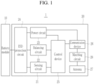
- FIG. 1 is a structural diagram schematically showing the battery pack according to embodiments.
- the battery pack 1 may include a battery module 10 and a battery management system (BMS) 20.
- BMS battery management system
- the battery module 10 may include a plurality of battery cells connected in series and/or in parallel.
- the BMS 20 may include a sensing circuit (or a detection circuit) 21, a balancing circuit 22, a power circuit (or a power supply circuit) 23, a control device 25, a communication device 26, an antenna (e.g., pattern antenna) 27, and a matching circuit (e.g., impedance-matching circuit) 28.
- the sensing circuit 21 may detect a cell voltage, a module voltage, a temperature, or the like from the battery module 10, and may transfer the detection result to the control device 25.
- the balancing circuit 22 may perform a balancing function between the battery cells of the battery module 10 under a control of the control device 25.
- the power circuit 23 may receive the module voltage supplied from the battery module 10, and may use the received module voltage to supply driving power for driving the control device 25 and the communication device 26 that will be described later.
- the BMS 20 may further include an electrostatic discharge (ESD) protection circuit 24 located between the battery module 10 and at least one of the sensing circuit 21, the balancing circuit 22, or the power circuit 23.
- the ESD protection circuit 24 may perform a function of protecting the BMS from an ESD and/or a surge flowing into the BMS 20 from the outside.
- the control device 25 may obtain state information (e.g., the cell voltage, the module voltage, the temperature, or the like) of the battery module 10 through the sensing circuit 21, and may perform state diagnosis of the battery module 10 based on the state information.
- the control device 25 may transmit the state information, diagnosis information, or the like, which is detected from the battery module 10, to an upper controller through wireless communication.
- the control device 25 may control a balancing of the battery module 10 by controlling the balancing circuit 22 based on the state information of the battery module 10.
- the control device 25 may include an analog front end (AFE) integrated circuit (IC).
- AFE analog front end
- the communication device 26 and the antenna 27 may be used for wireless communication between the control device 25 and the upper controller.
- the communication device 26 may transmit and receive a wireless signal of a frequency band (e.g., a predetermined frequency band) through the antenna 27 to communicate with the upper controller.
- the communication device 26 may transmit information received from the control device 25 to the upper controller through the antenna 27.
- the communication device 26 may transfer a signal received from the upper controller through the antenna 27 to the control device 25.
- the communication device 26 may include a radio frequency (RF) IC.
- RF radio frequency
- the antenna 27 may radiate a signal received from the communication device 26 as a wireless signal, and/or may receive a wireless signal transmitted from the upper controller to transfer the received signal to the communication device 26.
- the antenna 27 is configured in the form of a pattern antenna.
- the pattern antenna may be patterned using a conductive material on one surface of a printed circuit board (PCB) 30 of FIG. 4 on which the BMS 20 is mounted.
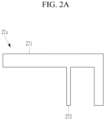
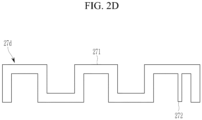
- FIGS. 2A to 2G show examples of the antenna 27 implemented as the pattern antenna.
- the antenna 27a, 27b, 27c, or 27d may include an antenna body 271 that is bent one or more times, and a wire-shaped signal transfer pattern 272 protruding from the antenna body 271.
- the antenna 27a of FIG. 2A may include an F-shaped antenna pattern.
- the F-shaped antenna pattern may include an extended portion extending from an upper end of the antenna body 271 and the signal transfer pattern 272 extends parallel to the extended portion. The extended portion at the upper end may be used to connect to a ground pattern 314 as explained further below.
- the pattern antennas 27b and 27c of FIGS. 2B and 2C may include a shape that is slightly modified from the F-shaped antenna 27a of FIG. 2A .
- the antenna pattern of the antennas 27b and 27c may include a reversely extending portion which extends from an end of the extended portion at the upper end toward the signal transfer pattern 272 while remaining spaced from the signal transfer pattern 272 to avoid interference.
- the antenna 27d of FIG. 2D may have a shape in which one end portion of the F-shaped antenna 27a of FIG. 2A is extended, e.g. from a base portion of the (F-shaped) antenna body 271, and the extended portion may include a serpentine shape by repeatedly bending the extended portion.
- the antenna 27e, 27f, or 27g may include a planar-shaped antenna body 271 and a wire-shaped signal transfer pattern 272 protruding from the planar-shaped antenna body 271.
- a pattern shape, a pattern area, a pattern width, or the like of the antenna 27 may be variously modified.
- the antenna body 271 of the antenna 27 may be bent 1 time (see FIG. 2A ), may be bent 2 times (see FIGS. 2B and 2C ), and may be bent 10 times (see FIG. 2D ), but various modifications are possible in a direction in which the antenna body 271 is bent, the number of times the antenna body 271 is bent, and the like.
- the signal transfer pattern 272 may be a straight-wire shape shown in FIGS. 2A , 2B , and 2D to 2G , or may be a bent wire shape shown in FIG. 2C .
- the antenna 27 may be patterned on the PCB with a metal or an alloy material depending on a suitable electrical conductivity, a suitable electrical property, or a suitable mechanical property, such as ductility or the like.
- the antenna 27 may be formed by patterning an antenna pattern of a corresponding shape on one surface of the PCB using a metal material, such as copper, tin, silver, gold, or the like.
- the matching circuit 28 may be connected between the communication device 26 and the antenna 27.
- FIG. 3 shows an example of the matching circuit 28.
- the matching circuit 28 may include an inductor L connected on a signal transfer path between the communication device 26 and the antenna 27, may include a capacitor C1 connected between a ground and a node n1 that is between the communication device 26 and the inductor L, and may include a capacitor C2 connected between a ground and a node n2 that is between the inductor L and the antenna 27.
- the matching circuit 28 may function to adjust the antenna 27 to match a desired communication frequency band by matching impedances seen from an input side and an output side of the matching circuit 28.
- the matching circuit 28 may function to compensate for a characteristic of the antenna 27 being deteriorated due to a characteristic of the flexible printed circuit board (PCB) if the antenna 27 is coupled to the flexible PCB.
- the antenna 27 on one surface of the flexible PCB may be formed so that a frequency of the antenna 27 matches a frequency band near the desired communication frequency band (e.g., a 2.4 GHz band), and the matching circuit 28 may precisely adjust an impedance so that the frequency of the antenna 27 closely matches a center frequency of the desired communication frequency band (e.g., about 2.44 GHz).
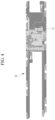
- the BMS 20 may further include the flexible PCB 30 of FIG. 4 on which the pattern antenna 27 is mounted. Further components that are mounted on the flexible PCB 30 may be the sensing circuit 21, the balancing circuit 22, the power circuit 23, the ESD protection circuit 24, the control device 25, the communication device 26, the antenna 27, and/or the matching circuit 28.
- the sensing circuit 21, the balancing circuit 22, the power circuit 23, the ESD protection circuit 24, the control device 25, the communication device 26, the antenna 27, and/or the matching circuit 28 of the BMS 20 may be mounted on the flexible PCB 30, and may be mounted within the battery pack 1.
- FIG. 4 shows an example of the flexible PCB of the BMS 20 according to embodiments.
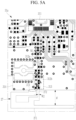
- FIGS. 5A and 5B are enlarged views of a portion 31 of the flexible PCB of FIG. 4 that is a portion of a region where a radio frequency (RF) block for wireless communication is located, and show an upper surface 31a and a lower surface 31b, respectively.
- RF radio frequency
- a plurality of components that include a radio frequency integrated circuit (RFIC) included in the communication device 26, the inductor L and the capacitors C1 and C2 included in the matching circuit 28, and the like, may be mounted on the upper surface 31a (e.g., a first surface) of the flexible PCB 30, and the antenna 27 may be formed on the upper surface 31a of the flexible PCB 30.
- RFIC radio frequency integrated circuit
- a first trace 312a and/or a second trace 312b for transferring a signal between the radio frequency integrated circuit and the antenna 27 may be formed between the antenna 27 and a region 311 where the radio frequency integrated circuit is coupled on the upper surface 31a of the flexible PCB 30.
- the trace 312a may be a signal transfer wire connected between the communication device 26 including the radio frequency integrated circuit and the matching circuit 28, and may be a straight-line shape that is not bent.
- the trace 312b may be a signal transfer wire connected between the trace 312a and the antenna 27, and may pass through a region 313 where the matching circuit 28 is mounted.
- a width W1 of the trace 312a or 312b may be determined for the impedance matching.
- a ground pattern (e.g., second ground pattern) 314 may be formed around the traces 312a and 312b to surround the traces 312a and 312b (e.g., in plan view), and the ground pattern 314 may be spaced apart from the traces 312a and 312b by an interval (e.g., a predetermined interval, for example, 0.15 mm).
- the antenna 27 is mounted on the upper surface 31a of the flexible PCB 30.
- the signal transfer pattern 272 of the antenna 27 may be connected to the trace 312b.
- a signal between the antenna 27 and the radio frequency integrated circuit may be transferred through the signal transfer pattern 272 of the antenna 27 and the traces 312a and 312b.
- the signal transfer pattern 272 of the antenna 27 may have the same width W2 as that of the trace 312a or 312b.
- the antenna 27 may be formed so that at least a portion of the pattern antenna is connected to a ground. Referring to FIG. 5A , a portion 273 of the antenna 27 may be connected to the ground pattern 314. The antenna 27 may ensure a sufficient distance (e.g., 5.8 mm or more) d between the ground pattern 314 and one end portion of the pattern antenna 27 not connected to the ground pattern 314 to avoid interference.
- the ground pattern 314 may refer to a conductor layer connected to a ground.
- the flexible PCB 30 includes a fill-cut pattern 322.
- the fill-cut pattern 322 is formed on the lower surface 31b of the flexible PCB 30.
- the fill-cut pattern 322 is a pattern in which a portion of a ground pattern (e.g., first ground pattern) 321 on the lower surface 31b of the flexible PCB 30 is removed in a line shape. That is, the fill-cut pattern 322 may be a pattern in which a portion of a bare board of the flexible PCB 30 is exposed to the outside in a line shape.
- the fill-cut pattern 322 may be on the lower surface 31b of the flexible PCB 30 between a region 325 that corresponds to the radio frequency integrated circuit and a region 324 that corresponds to the antenna 27.
- the fill-cut pattern 322 is formed on the lower surface 31b to cover, e.g. overlap, a region where the traces 312a and/or 312b are formed.
- the fill-cut pattern 322 is formed in a region corresponding to a region where the traces 312a and 312b of the upper surface 31a are to thereby cover a region where the traces 312a and 312b are, e.g., in a plan view.
- a width W3 of the fill-cut pattern 322 may be wider than the width W1 of the trace 312a or 312b so that the entire traces 312a and 312b may be covered by the fill-cut pattern 322.
- the width relation further improves matching performance. For example, if the width W1 of the trace 312a or 312b is 0.5 mm, the width W3 of the fill-cut pattern 322 may be 0.75 mm.
- the flexible PCB 30 may further include a plurality of via holes 323 adjacent to the fill-cut pattern 322.
- the region 324 corresponding to the antenna 27 may be formed so as not to dispose any conductive pattern (e.g., a ground pattern) on the lower surface 31b of the flexible PCB 30.
- the BMS 20 is configured using the flexible PCB 30 in the battery pack 1, precise frequency matching is possible using the antenna 27 and the matching circuit 28 on one surface of the flexible PCB 30, the fill-cut pattern 322 on the other surface of the flexible PCB 30. A further improvement of the frequency matching can be reached through the plurality of via holes 323 formed around the fill-cut pattern 322. Therefore, by improving matching performance for the desired communication frequency band, wireless communication performance (e.g., transmission output and reception sensitivity) of the BMS 20 may be improved, and robustness of the wireless communication may be secured.
- wireless communication performance e.g., transmission output and reception sensitivity
- Electronic or electrical devices may be realized by using appropriate hardware, firmware (e.g., an application-specific integrated circuit), software, or combinations of software, firmware, and hardware.
- firmware e.g., an application-specific integrated circuit
- various configurations of the above-noted devices may be positioned on one integrated circuit (IC) chip or an individual IC chip.
- various configurations of the above-noted devices may be realized on a flexible printed circuit film, a tape carrier package (TCP), a printed circuit board (PCB), or one substrate.
- TCP tape carrier package
- PCB printed circuit board
- the electrical or mutual connections described in the present specification may, for example, be realized by the PCB, wires on different types of circuit carriers, or conductive elements.
- the conductive elements may, for example, include metallization, such as surface metallizations and/or pins, and may include conductive polymers or ceramics.
- the various configurations of the devices may be performed by at least one processor so as to perform the above-described various functions, they may be performed in at least one computing device, and they may be processes or threads for performing computer program instructions and interacting with other system constituent elements.
- the computer program instruction is stored in a memory realizable in a computing device using a standard memory device, such as a random access memory (RAM).
- the computer program instruction may also be stored in a non-transitory computer readable medium, such as a CD-ROM or a flash drive.
- battery pack 10 battery module 20: battery management system 21: sensing circuit 22: balancing circuit 23: power circuit 24: ESD protection circuit 25: control unit 26: communication device 27, 27a - 27g: antenna 28: matching circuit 30: flexible PCB 312a, 312b: trace 322: fill-cut pattern 323: via hole 314, 321: ground pattern
Landscapes
- Engineering & Computer Science (AREA)
- Microelectronics & Electronic Packaging (AREA)
- Chemical Kinetics & Catalysis (AREA)
- Chemical & Material Sciences (AREA)
- Electrochemistry (AREA)
- General Chemical & Material Sciences (AREA)
- Computer Networks & Wireless Communication (AREA)
- Signal Processing (AREA)
- Power Engineering (AREA)
- Physics & Mathematics (AREA)
- Electromagnetism (AREA)
- Manufacturing & Machinery (AREA)
- Battery Mounting, Suspending (AREA)
- Details Of Aerials (AREA)
- Charge And Discharge Circuits For Batteries Or The Like (AREA)
Applications Claiming Priority (1)
| Application Number | Priority Date | Filing Date | Title |
|---|---|---|---|
| KR1020230065163A KR20240167298A (ko) | 2023-05-19 | 2023-05-19 | 인쇄회로기판, 및 이를 포함하는 배터리 관리 시스템 및 배터리 팩 |
Publications (1)
| Publication Number | Publication Date |
|---|---|
| EP4465447A1 true EP4465447A1 (de) | 2024-11-20 |
Family
ID=91128164
Family Applications (1)
| Application Number | Title | Priority Date | Filing Date |
|---|---|---|---|
| EP24175979.4A Pending EP4465447A1 (de) | 2023-05-19 | 2024-05-15 | Leiterplatte und batterieverwaltungssystem und batteriepack damit |
Country Status (4)
| Country | Link |
|---|---|
| US (1) | US20240388106A1 (de) |
| EP (1) | EP4465447A1 (de) |
| KR (1) | KR20240167298A (de) |
| CN (1) | CN119012496A (de) |
Citations (4)
| Publication number | Priority date | Publication date | Assignee | Title |
|---|---|---|---|---|
| KR20090133072A (ko) * | 2008-06-23 | 2009-12-31 | (주)기가레인 | 인쇄회로기판과 일체로 형성되는 안테나 |
| CN102738569A (zh) * | 2012-03-31 | 2012-10-17 | 苏州市吴通天线有限公司 | 一种宽频pcb天线 |
| US20170085000A1 (en) * | 2014-03-26 | 2017-03-23 | Thomson Licensing | An antenna structure with dielectric loading |
| US20220029204A1 (en) * | 2019-02-01 | 2022-01-27 | Lg Energy Solution, Ltd. | Battery system and slave battery management system |
-
2023
- 2023-05-19 KR KR1020230065163A patent/KR20240167298A/ko active Pending
- 2023-10-27 US US18/496,510 patent/US20240388106A1/en active Pending
-
2024
- 2024-05-15 EP EP24175979.4A patent/EP4465447A1/de active Pending
- 2024-05-20 CN CN202410624674.2A patent/CN119012496A/zh active Pending
Patent Citations (4)
| Publication number | Priority date | Publication date | Assignee | Title |
|---|---|---|---|---|
| KR20090133072A (ko) * | 2008-06-23 | 2009-12-31 | (주)기가레인 | 인쇄회로기판과 일체로 형성되는 안테나 |
| CN102738569A (zh) * | 2012-03-31 | 2012-10-17 | 苏州市吴通天线有限公司 | 一种宽频pcb天线 |
| US20170085000A1 (en) * | 2014-03-26 | 2017-03-23 | Thomson Licensing | An antenna structure with dielectric loading |
| US20220029204A1 (en) * | 2019-02-01 | 2022-01-27 | Lg Energy Solution, Ltd. | Battery system and slave battery management system |
Non-Patent Citations (2)
| Title |
|---|
| TSOI MAN HO ET AL: "Planar Antenna Design for Internet of Things Applications", INTECHOPEN, 23 September 2020 (2020-09-23), XP093207969, Retrieved from the Internet <URL:https://www.intechopen.com/chapters/72152> [retrieved on 20240924] * |
| WALLACE RICHARD: "Application Note AN058, Antenna Selection Guide", TEXAS INSTRUMENTS, 1 January 2010 (2010-01-01), pages 1 - 45, XP055933845, Retrieved from the Internet <URL:https://www.ti.com/lit/an/swra161b/swra161b.pdf?ts=1655783707925> [retrieved on 20220621] * |
Also Published As
| Publication number | Publication date |
|---|---|
| CN119012496A (zh) | 2024-11-22 |
| KR20240167298A (ko) | 2024-11-26 |
| US20240388106A1 (en) | 2024-11-21 |
Similar Documents
| Publication | Publication Date | Title |
|---|---|---|
| JP5174790B2 (ja) | バッテリパック | |
| US20250015443A1 (en) | Battery module with flexible interconnector | |
| US12142816B2 (en) | Antenna module and method for inspecting antenna module | |
| EP2131412A2 (de) | Batteriepack | |
| CN104704679B (zh) | 信号线路模块和通信终端装置 | |
| KR20150018412A (ko) | 배터리 팩 | |
| JP2004103248A (ja) | バッテリーパックおよび電磁気ノイズシールドパッチならびに電磁気ノイズシールド方法 | |
| JP2011119413A (ja) | カード型無線通信モジュール | |
| US20130194771A1 (en) | Battery pack | |
| EP1875532B1 (de) | Eine auf einer pcb strukturierte schleifenantenne enthaltende sekundärbatterie | |
| CN110380198A (zh) | 一种天线模组及电子设备 | |
| EP4465447A1 (de) | Leiterplatte und batterieverwaltungssystem und batteriepack damit | |
| US20220121898A1 (en) | Rfid tag | |
| KR101288059B1 (ko) | 배터리 보호회로의 패키지 모듈 | |
| EP3843009A1 (de) | Rfid-etikettensubstrat, rfid-etikett und rfid-system | |
| US12333369B2 (en) | Circuit module and RFID tag | |
| US20250048533A1 (en) | Multilayer board, multilayer board module, and electronic device | |
| EP3758453A1 (de) | Schalttafel | |
| US20260088374A1 (en) | Battery system | |
| CN208188872U (zh) | 元器件内置装置及rfid标签 | |
| KR101429766B1 (ko) | 전지 팩 | |
| KR100624908B1 (ko) | 안테나 패턴을 갖는 배터리 팩 | |
| WO2024116330A1 (ja) | 電子基板ユニット及び電池監視システム | |
| CN114695977A (zh) | 复合电池和电子设备 | |
| CN117175212A (zh) | 具有通信及感测功能的移动装置 |
Legal Events
| Date | Code | Title | Description |
|---|---|---|---|
| PUAI | Public reference made under article 153(3) epc to a published international application that has entered the european phase |
Free format text: ORIGINAL CODE: 0009012 |
|
| STAA | Information on the status of an ep patent application or granted ep patent |
Free format text: STATUS: REQUEST FOR EXAMINATION WAS MADE |
|
| 17P | Request for examination filed |
Effective date: 20240515 |
|
| AK | Designated contracting states |
Kind code of ref document: A1 Designated state(s): AL AT BE BG CH CY CZ DE DK EE ES FI FR GB GR HR HU IE IS IT LI LT LU LV MC ME MK MT NL NO PL PT RO RS SE SI SK SM TR |
|
| GRAP | Despatch of communication of intention to grant a patent |
Free format text: ORIGINAL CODE: EPIDOSNIGR1 |
|
| STAA | Information on the status of an ep patent application or granted ep patent |
Free format text: STATUS: GRANT OF PATENT IS INTENDED |
|
| RIC1 | Information provided on ipc code assigned before grant |
Ipc: H01Q 9/04 20060101AFI20260324BHEP Ipc: H01M 10/42 20060101ALI20260324BHEP Ipc: H01Q 9/40 20060101ALI20260324BHEP Ipc: H01Q 9/42 20060101ALI20260324BHEP Ipc: H01P 3/00 20060101ALI20260324BHEP Ipc: H01Q 1/38 20060101ALN20260324BHEP |