EP4465369A1 - Wafer having micro-led structure, production method for wafer having micro-led structure, and production method for junction-type semiconductor wafer having micro-led structure - Google Patents
Wafer having micro-led structure, production method for wafer having micro-led structure, and production method for junction-type semiconductor wafer having micro-led structure Download PDFInfo
- Publication number
- EP4465369A1 EP4465369A1 EP22920523.2A EP22920523A EP4465369A1 EP 4465369 A1 EP4465369 A1 EP 4465369A1 EP 22920523 A EP22920523 A EP 22920523A EP 4465369 A1 EP4465369 A1 EP 4465369A1
- Authority
- EP
- European Patent Office
- Prior art keywords
- micro
- wafer
- led
- led structure
- epitaxial layer
- Prior art date
- Legal status (The legal status is an assumption and is not a legal conclusion. Google has not performed a legal analysis and makes no representation as to the accuracy of the status listed.)
- Pending
Links
Images








Classifications
-
- H—ELECTRICITY
- H10—SEMICONDUCTOR DEVICES; ELECTRIC SOLID-STATE DEVICES NOT OTHERWISE PROVIDED FOR
- H10H—INORGANIC LIGHT-EMITTING SEMICONDUCTOR DEVICES HAVING POTENTIAL BARRIERS
- H10H20/00—Individual inorganic light-emitting semiconductor devices having potential barriers, e.g. light-emitting diodes [LED]
- H10H20/80—Constructional details
- H10H20/81—Bodies
- H10H20/819—Bodies characterised by their shape, e.g. curved or truncated substrates
-
- H—ELECTRICITY
- H10—SEMICONDUCTOR DEVICES; ELECTRIC SOLID-STATE DEVICES NOT OTHERWISE PROVIDED FOR
- H10H—INORGANIC LIGHT-EMITTING SEMICONDUCTOR DEVICES HAVING POTENTIAL BARRIERS
- H10H20/00—Individual inorganic light-emitting semiconductor devices having potential barriers, e.g. light-emitting diodes [LED]
- H10H20/01—Manufacture or treatment
- H10H20/011—Manufacture or treatment of bodies, e.g. forming semiconductor layers
- H10H20/013—Manufacture or treatment of bodies, e.g. forming semiconductor layers having light-emitting regions comprising only Group III-V materials
-
- H—ELECTRICITY
- H10—SEMICONDUCTOR DEVICES; ELECTRIC SOLID-STATE DEVICES NOT OTHERWISE PROVIDED FOR
- H10H—INORGANIC LIGHT-EMITTING SEMICONDUCTOR DEVICES HAVING POTENTIAL BARRIERS
- H10H20/00—Individual inorganic light-emitting semiconductor devices having potential barriers, e.g. light-emitting diodes [LED]
- H10H20/01—Manufacture or treatment
- H10H20/011—Manufacture or treatment of bodies, e.g. forming semiconductor layers
- H10H20/018—Bonding of wafers
-
- H—ELECTRICITY
- H10—SEMICONDUCTOR DEVICES; ELECTRIC SOLID-STATE DEVICES NOT OTHERWISE PROVIDED FOR
- H10H—INORGANIC LIGHT-EMITTING SEMICONDUCTOR DEVICES HAVING POTENTIAL BARRIERS
- H10H20/00—Individual inorganic light-emitting semiconductor devices having potential barriers, e.g. light-emitting diodes [LED]
- H10H20/80—Constructional details
- H10H20/81—Bodies
- H10H20/813—Bodies having a plurality of light-emitting regions, e.g. multi-junction LEDs or light-emitting devices having photoluminescent regions within the bodies
- H10H20/8132—Laterally arranged light-emitting regions, e.g. nano-rods
-
- H—ELECTRICITY
- H10—SEMICONDUCTOR DEVICES; ELECTRIC SOLID-STATE DEVICES NOT OTHERWISE PROVIDED FOR
- H10H—INORGANIC LIGHT-EMITTING SEMICONDUCTOR DEVICES HAVING POTENTIAL BARRIERS
- H10H20/00—Individual inorganic light-emitting semiconductor devices having potential barriers, e.g. light-emitting diodes [LED]
- H10H20/80—Constructional details
- H10H20/81—Bodies
- H10H20/822—Materials of the light-emitting regions
- H10H20/824—Materials of the light-emitting regions comprising only Group III-V materials, e.g. GaP
-
- H—ELECTRICITY
- H10—SEMICONDUCTOR DEVICES; ELECTRIC SOLID-STATE DEVICES NOT OTHERWISE PROVIDED FOR
- H10H—INORGANIC LIGHT-EMITTING SEMICONDUCTOR DEVICES HAVING POTENTIAL BARRIERS
- H10H20/00—Individual inorganic light-emitting semiconductor devices having potential barriers, e.g. light-emitting diodes [LED]
- H10H20/80—Constructional details
- H10H20/83—Electrodes
- H10H20/831—Electrodes characterised by their shape
-
- H—ELECTRICITY
- H10—SEMICONDUCTOR DEVICES; ELECTRIC SOLID-STATE DEVICES NOT OTHERWISE PROVIDED FOR
- H10H—INORGANIC LIGHT-EMITTING SEMICONDUCTOR DEVICES HAVING POTENTIAL BARRIERS
- H10H20/00—Individual inorganic light-emitting semiconductor devices having potential barriers, e.g. light-emitting diodes [LED]
- H10H20/80—Constructional details
- H10H20/83—Electrodes
- H10H20/831—Electrodes characterised by their shape
- H10H20/8314—Electrodes characterised by their shape extending at least partially onto an outer side surface of the bodies
-
- H—ELECTRICITY
- H10—SEMICONDUCTOR DEVICES; ELECTRIC SOLID-STATE DEVICES NOT OTHERWISE PROVIDED FOR
- H10H—INORGANIC LIGHT-EMITTING SEMICONDUCTOR DEVICES HAVING POTENTIAL BARRIERS
- H10H20/00—Individual inorganic light-emitting semiconductor devices having potential barriers, e.g. light-emitting diodes [LED]
- H10H20/80—Constructional details
- H10H20/81—Bodies
- H10H20/817—Bodies characterised by the crystal structures or orientations, e.g. polycrystalline, amorphous or porous
Definitions
- the present invention relates to a wafer having a micro-LED structure, a method for manufacturing a wafer having a micro-LED structure, and a method for manufacturing a bonded semiconductor wafer having a micro-LED structure.
- a technique to separate parts necessary to function as light-emitting devices (hereinafter, referred to as functional layers) out of laminates epitaxially grown on starting substrates (hereinafter referred to as epitaxial layer structures) from starting substrates and transfer the parts to another substrate is an important technique to mitigate restriction due to physical properties of the starting substrates and to increase the degree of freedom in designing device systems.
- the technique to realize the transferring is necessary in which the functional layer is bonded to a permanent substrate to obtain a bonded substrate and then the starting substrate is removed from this bonded substrate, or the starting substrate is removed while the function layer being held by a temporary support substrate and then the function layer is bonded to the permanent substrate, and the like.
- Patent Document 1 discloses a technique for thermo-compressionally bonding a semiconductor epitaxial substrate to a temporary supporting substrate via a dielectric layer and a technique for separating a temporary supporting substrate and an epitaxial functional layer by wet etching.
- Patent Document 2 discloses a technique in which a sacrificial layer and a semiconductor crystal layer are formed on a single crystal layer of a starting substrate in this order, and an isolation groove is formed to the semiconductor crystal layer to expose the sacrificial layer, and then the semiconductor crystal layer is bonded to a transfer substrate, and then sacrificial-layer etching is performed via the isolation groove, thereby separating the starting substrate.
- Manufacturing of a micro-LED having a miniaturized light-emitting device portion can be realized using these techniques; however, no improvement measures toward the brightness decrease have not been presented.
- An object of the present invention is to provide a wafer having a micro-LED structure in which generation of a brightness decrease is suppressed; a method for manufacturing the wafer having a micro-LED structure in which generation of a brightness decrease is suppressed; and a method for manufacturing a bonded semiconductor wafer having a micro-LED structure in which generation of a brightness decrease is suppressed.
- the present invention provides a wafer having a micro-LED structure, the wafer comprising:
- the micro-LED structure constituted on the wafer is constituted by the first structure and the second structure of the epitaxial layer structures selectively grown in a state separated by the mask in advance; thus, device-isolation processing is not necessary; in addition, since the polarity of the electrode of the first structure is different from that of the electrode of the second structure, one of the electrodes can make contact with an N-type electrode and the other of the electrodes can make contact with a P-type electrode, resulting in eliminating a need for processing such as dry etching of the epitaxial layer structure to form electrodes.
- the inventive wafer having a micro-LED structure can provide the micro-LED structure, in which brightness decrease due to damage originated by the processing such as the device-isolation processing and electrode-forming processing is suppressed.
- the micro-LED structure With a transfer of the micro-LED structure from the inventive wafer having a micro-LED structure to a substrate suitable for a micro-LED device, the micro-LED device having the micro-LED structure with excellent brightness can be produced.
- the plurality of the epitaxial layer structures have thin films which are full depletion layers in ⁇ 111 ⁇ plane directions.
- an insulating property between the electrodes can be secured.
- the first structure is the light-emitting device portion having an AlGaInP-based light-emitting layer and Lh ⁇ 0.707 ⁇ Lws where a width of a shortest portion at a bottom is Lws, and a total thickness of the first structure in a direction perpendicular to a surface of the starting substrate is Lh.
- all epitaxial layers necessary to function as the light-emitting device portion can be made to grow in accordance with the design thickness in the [001] direction perpendicular to the starting substrate surface.
- the width Lws of the shortest portion at the bottom of the first structure may be 10 um or more and 100 um or less.
- the inventive wafer having a micro-LED structure even when the micro-LED structure has the width Lws of the shortest portion of the bottom of the first structure with 10 um or more and 100 um or less, the generation of brightness decrease can be sufficiently suppressed.
- the epitaxial layer structure includes an active layer
- the second structure is a non-light-emitting device portion and includes a pyramid-shape bridge portion at least partially, and 1.5 um ⁇ W ⁇ T/0.707 where a width of a shortest part of the bridge portion is W [pm] and a sum of thicknesses of the epitaxial layer structure up to the active layer in the direction perpendicular to the surface of the starting substrate is T [um].
- a bridge portion of the second structure can be pyramid-shape having no flat portion before reaching the second conductivity-type layer.
- W > 1.5 um a thickness of a first conductivity-type cladding layer necessary to make contact with a first conductivity-type electrode can be ensured.
- the present invention provides a wafer having a micro-LED structure, the wafer comprising:
- the wafer having a micro-LED structure according to another aspect of the present invention may not have a mask.
- the micro-LED structure constituted on the wafer is constituted by the first structure and the second structure of epitaxial layer structures, each of which is selectively grown, device-isolation processing is not necessary.
- the polarity of the electrode of the first structure is different from that of the electrode of the second structure.
- one of the electrodes can make contact with an N-type electrode and the other of the electrodes can make contact with a P-type electrode, resulting in eliminating a need for processing, such as dry etching, to the epitaxial layer structure to form the electrodes.
- the wafer having a micro-LED structure according to this aspect can provide the micro-LED structure, in which brightness decrease due to damage originated by the processing such as the device-isolation processing and the electrode-forming processing is suppressed.
- the micro-LED device can be produced in which the micro-LED structure that shows excellent brightness is provided.
- the present invention provides a method for manufacturing a wafer having a micro-LED structure, the method comprising:
- the wafer having a micro-LED structure manufactured by such a manufacturing method has the micro-LED structure constituted by the first structure and the second structure of the epitaxial layer structures selectively grown in a state separated by the mask in advance.
- Such a micro-LED structure has no need for device-isolation processing.
- the polarity of the electrode of the first structure is different from that of the electrode of the second structure, one of the electrode can make contact with an N-type electrode and the other of the electrodes can make contact with a P-type electrode, resulting in eliminating a need for processing to form the electrodes.
- the wafer having a micro-LED structure can be manufactured, in which brightness decrease due to damage originated by the processing such as the device-isolation processing and the electrode-forming processing is suppressed.
- the present invention provides a method for manufacturing a bonded semiconductor wafer having a micro-LED structure, the method comprising:
- the wafer having a micro-LED structure is manufactured in accordance with the inventive method for manufacturing the inventive wafer having a micro-LED structure and used for manufacturing the bonded semiconductor wafer.
- the bonded semiconductor wafer can be manufactured, the bonded semiconductor wafer having a micro-LED structure, in which brightness decrease due to damage originated by the processing such as the device-isolation processing and the electrode-forming processing is suppressed.
- the inventive wafer having a micro-LED structure it is possible to have the micro-LED structure, in which brightness decrease due to damage originated by the processing such as the device-isolation processing and the electrode-forming processing is suppressed.
- the micro-LED structure with a transfer of the micro-LED structure from the inventive wafer having a micro-LED structure to a substrate suitable for a micro-LED device, the micro-LED device having the micro-LED structure that exhibits excellent brightness can be produced.
- the wafer having a micro-LED structure in which brightness decrease due to damage originated by the processing such as the device-isolation processing and the electrode-forming processing is suppressed, can be manufactured.
- the bonded semiconductor wafer having a micro-LED structure in which brightness decrease due to damage originated by the processing such as the device-isolation processing and the electrode-forming processing is suppressed, can be manufactured.
- the present inventor focuses on the fact that while an epitaxial layer structure, which is to be a micro-LED structure, is epitaxially grown to an opening of a mask pattern provided on a starting substrate, by making a V/III ratio of raw materials to 1 or more and 50 or less, ⁇ 111 ⁇ planes with slow growth speed appear along with a growth of a (001) plane parallel to a surface of a starting substrate, resulting in the epitaxial layer structure capable of forming pyramid-shape or truncated pyramid-shape.
- the present inventor focuses on the fact that a thickness of the layer of a slope becomes significantly thin compared with a thickness in a direction perpendicular to the surface of the substrate (hereinafter, [001] direction) in such a shapes and thus full depletion of unneeded layers is possible by adjusting a size of the opening and the V/III ratio of the raw materials.
- the present inventor has earnestly studied on such steps and found that a pair of the epitaxial layer structures in the pyramid-shape or the truncated pyramid-shape, each selectively grown, can be used as the micro-LED structure without processing for device-separation or electrode formation. This finding has led to the completion of the present invention.
- the present invention is a wafer having a micro-LED structure, the wafer comprising:
- the present invention is a wafer having a micro-LED structure, the wafer comprising:
- the present invention is a method for manufacturing a wafer having a micro-LED structure, the method comprising:
- the present invention is a method for manufacturing a bonded semiconductor wafer having a micro-LED structure, the method comprising:
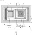
- FIG. 1 is a plane view
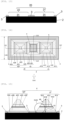
- FIG. 2 is a projection view (side view) of FIG. 1 from a II direction.
- the wafer 1 having a micro-LED structure shown in FIGs. 1 and 2 includes a starting substrate 2, a mask 3 formed on this starting substrate 2 with a mask pattern including an opening (not shown in FIG. 1 and FIG. 2 ), and a plurality of epitaxial layer structures 4 each of which selectively grown on a portion corresponding to the opening of the mask pattern on the starting substrate 2 (not shown in FIGs. 1 and 2 ).
- Each of the plurality of the epitaxial layer structures 4 has a pyramid-shape or a truncated pyramid-shape surrounded by ⁇ 111 ⁇ planes 4A.
- the plurality of the epitaxial layer structures 4 includes a first structure 41, as a light-emitting device portion, and a second structure 42 connected to the first structure 41.
- the first structure 41 includes an electrode 5.
- the second structure 42 includes an electrode 6.
- the electrodes 5 and 6 are of different polarities from each other.
- the first structure 41 and the second structure 42 constitute a micro-LED structure 7 operable as one micro-LED.
- the micro-LED structure 7 constituted on the wafer 1 is constituted by the first structure 41 and the second structure 42 of the epitaxial layer structures 4 each of which selectively grown in a state separated by the mask 3 in advance; thus, device-isolation processing is not necessary.
- the polarity of the electrode 5 of the first structure 41 is different from that of the electrode 6 of the second structure 42, and one of the electrodes can make contact with an N-type electrode and the other of the electrodes can make contact with a P-type electrode, resulting in eliminating a need for processing such as dry etching of the epitaxial layer structure to form electrodes. Consequently, the wafer 1 having a micro-LED structure 7 shown in FIGs.
- the micro-LED device 1 and 2 can provide the micro-LED structure 7, in which brightness decrease due to damage originated by the processing such as the device-isolation processing and an electrode-forming processing is suppressed.
- the micro-LED device can be produced in which the micro-LED structure 7 that shows excellent brightness is provided.
- a first conductivity-type GaAs substrate can be used without limitation.
- the starting substrate 2 may have a buffer layer (not shown), for example, a first conductivity-type GaAs buffer layer on a surface thereof.
- the GaAs buffer layer typically has a thickness of 0.5 ⁇ m.
- the mask 3 forms, for example, a nonpolar dielectric film such as SiO 2 or silicon nitride, and forms the mask pattern made of the nonpolar dielectric film having the openings.
- a region where the first structure 41 is formed has, for example, a rectangular planar shape.
- a region where the second structure 42 is formed is, for example, the region having all corners of right angles (90°).
- the openings of the mask pattern, the region in which the first structure 41 is formed and the region in which the second structure 42 is formed are described in a description of the inventive method for manufacturing the wafer having a micro-LED structure in a later section with reference to the drawings.
- the mask 3 includes a portion formed on a portion including a center of the starting substrate 2 and a portion formed on an outer edge portion of the substrate 2.
- the first structure 41 is the light-emitting device portion having the truncated pyramid-shape (also referred to as a pyramidal shape), in which a sacrificial layer 41A, a first cladding layer 41B, an active layer 41C, a second cladding layer 41D, an intermediate layer (not shown), and a window layer 41E are included in this order. Because the first structure 41 is a part of the epitaxial layer structure 4, these layers are the epitaxial layers.
- the sacrificial layer 41A can include, for example, an AlAs sacrificial layer, a GaInP sacrificial layer, and/or a GaAs sacrificial layer.
- the sacrificial layer 41A may be constituted by a plurality of layers.
- the sacrificial layer 41A is a first conductivity-type AlAs sacrificial layer having a thickness of 0.5 ⁇ m.
- the first cladding layer 41B is, for example, a first conductivity-type AlGaInP (for example, (Al y Ga 1-y ) x In 1-x P (0.4 ⁇ x ⁇ 0.6, 0 ⁇ y ⁇ 1)) first cladding layer.
- the first cladding layer 41B is the layer having "x" and "y" in the general formula as 0.5 and 0.85, respectively, and a thickness of 1.0 ⁇ m.
- the active layer 41C is, for example, a non-doped AlGaInP (for example, (Al y Ga 1-y ) x In 1-x P (0.4 ⁇ x ⁇ 0.6, 0 ⁇ y ⁇ 0.6))-based light emitting layer.
- the active layer 41C is the layer having "x" and "y" in the general formula above as 0.5 and 0.1, respectively, and having a thickness of 0.25 ⁇ m.
- the second cladding layer 41D is, for example, a second conductivity-type AlGaInP (for example, (Al y Ga 1-y ) x In 1-x P (0.4 ⁇ x ⁇ 0.6, 0 ⁇ y ⁇ 1)) second cladding layer.
- the second cladding layer 41D is the layer having "x" and "y" in the general formula above as 0.5 and 0.85, respectively, and a thickness of 0.75um.
- the intermediate layer not shown is, for example, a second conductivity-type GaInP intermediate layer, and is the layer having a thickness of 0.1 um in the first embodiment shown in FIGs. 1 and 2 .
- the window layer 41E is, for example, a second conductivity-type GaP window layer.
- the window layer 41E is the layer having a thickness of 1.9 ⁇ m.
- a width of a shortest portion at a bottom of the first structure 41 is Lws. Even when the width Lws of the shortest portion at the bottom of the first structure 41, as the light-emitting device portion, is 10 um or more and 100 um or less, i.e., a typical micro-LED size, the inventive wafer 1 having a micro-LED structure 7 can provide the micro-LED structure 7 in which brightness decrease due to damage originated by the processing is suppressed because the processing such as the device-isolation processing and electrode-forming processing is unnecessary.
- a total thickness of the first structure 41 in a direction perpendicular to a surface of the starting substrate 2 ([001] direction) is Lh. It is preferred that the total thickness Lh of the first structure 41 and the width Lws of the shortest portion at the bottom of the first structure 41 satisfy Lh ⁇ 0.707 ⁇ Lws.
- the first structure 41 having such a structure can be prevented from being a pyramid-shape with no flat portion on an apex before reaching a design thickness, thereby all epitaxial layers necessary to function as the light-emitting device portion can be made to grow in the [001] direction to the design thickness.
- the lower limit of the total thickness Lh is not particularly limited but is, for example, 0.5 ⁇ m.
- the second structure 42 is connected to the first structure 41. More specifically, the second structure 42 includes a pyramid-shaped bridge portion 43 at least partially, which is in contact with the first structure 41.
- the bridge portion 43 has a sacrificial layer 43A integrated with the sacrificial layer 41A of the first structure 41, and a stacked portion 43F on the layer 43A.
- the stacked portion 43F contains respective materials of the epitaxial layers of the first structure 41 but has the pyramid-shape so as to make the apex at a top layer of the first cladding layer. Consequently, only the ⁇ 111 ⁇ planes 4A are grown above the active layer, resulting in thin films. That is, the bridge portion 43 has a second conductivity-type layer being fully depleted, thus practically behaving as a first conductivity-type.
- the second structure 42 shown in FIGs. 1 and 2 further includes a sacrificial layer 42A, a first cladding layer 42B, an active layer 42C, a second cladding layer 42D, an intermediate layer (not shown), and a window layer 42E in this order as similar to the first structure 41, and these layers constitute a stacked portion 42F.
- the sacrificial layer 42A is integrated with the sacrificial layers 41A and 43A.
- the second structure 42 shown in FIGs. 1 and 2 is a non-light-emitting device portion.
- a width of a shortest part of the bridge portion 43 is W [pm].
- a sum of thicknesses of the epitaxial layer structure 4 up to the active layers 41C and 42C in the direction ([001] direction) perpendicular to the surface of the starting substrate 2 is T [pm]. In the first embodiment shown in FIGs. 1 and 2 , then 1.5 um ⁇ W ⁇ T/0.707.
- a bridge portion 43 of the second structure 42 can have a pyramid-shape having no flat portion before reaching the second conductivity-type layers.
- W > 1.5 um a thickness of a first conductivity-type cladding layer necessary to contact a first conductivity-type electrode can be ensured.
- a plurality of the epitaxial layer structures 4 in the first embodiment shown in FIGs. 1 and 2 , the first structure 41, and the second structure 42 including the stacked portion 42F and the bridge portion 43) have thin films which are full depletion layers in ⁇ 111 ⁇ plane 4A directions.
- the electrode 5 is formed with a material that allows a formation of an ohmic to a second conductivity-type semiconductor.
- the electrode 6 is formed with a material that allows a formation of an ohmic to a first conductivity-type semiconductor.
- the electrode 6 formed on the second structure 42 extends from the window layer 42E, which is the structural apex of the stacked portion 42F, to the bridge portion 43 and is in ohmic contact with the first conductivity-type bridge portion 43.
- a part of the electrode 6 is in contact with the second cladding layer 42D and the window layer 42E of the second structure 42, which is a non-light-emitting device portion, either directly or through the depletion layer; however, another part of the electrode 6 is in contact with the first conductivity-type bridge portion 43, thus being short-circuited state and not conducting current through a PiN junction, resulting in no electrical problem.
- the bridge portion 43 a part of the plurality of the epitaxial layer structures 4, has thin films which are full depletion layers in ⁇ 111 ⁇ plane 4A directions, an insulating property between the electrodes 5 and 6 can be secured as described above.
- an outermost periphery of the bridge portion 43 is covered with fully depleted ultrathin layers, and thus the insulating property between the electrodes is secured; however, when the effective V/III ratio on the surface increases due to a lower growth temperature in the formation process of the bridge portion 43, etc., the layer thickness on the slope may become large, resulting in leakage.
- a part of the stacked portion 43F of the bridge portion 43 may be removed by a method such as dry etching for making a stacked portion 43G to prevent the leakage.
- the second structure 42 as the non-light-emitting device portion, may only have the bridge portion 43 ( FIG. 5 : a plane view; FIG. 6 : a projection view of FIG. 5 from a VI direction (side view)).
- the stacked portion 42F of the second structure 42 which is the non-light-emitting device portion
- the first structure 41 which is the light-emitting device portion
- the portion 42F usually stops growth thereof when the GaP window layer 41E of the light-emitting device portion is stacked until design thickness, thus the non-light-emitting device portion is never higher than the light-emitting device portion, and the non-light-emitting device portion having a large height than that of the light-emitting device portion has no functional merit.
- it is suitable that the height of the stacked portion 42F of the second structure 42, as the non-light-emitting device portion is lower or equal to the height of the first structure 41, as the light-emitting device portion.
- FIG. 7 is a plane view
- FIG. 8 is a projection view (side view) of FIG. 7 from a VIII direction.
- the second embodiment shown in FIGs. 7 and 8 is the same as the first embodiment except that a shape of a first structure 41, as a light-emitting device portion, is changed.
- a rectangular-shaped device can be realized by making a size of the first structure 41, as the light-emitting device portion, horizontally long while keeping a size of a second structure 42, as a non-light-emitting device portion, intact.
- FIG. 9 is a plane view
- FIG. 10 is a projection view (side view) of FIG. 9 from an X direction.
- the third embodiment shown in FIGs. 9 and 10 is the same as the first embodiment except that a shape of a first structure 41, as a light-emitting device portion, is changed, and, in line with this, a shape of a bridge portion 43 of a second structure 42, which is a non-light-emitting device portion, is changed.
- a shape of a first structure 41 as a light-emitting device portion
- a shape of a bridge portion 43 of a second structure 42 which is a non-light-emitting device portion
- a wafer having a micro-LED structure according to another aspect of the present invention may not include a mask.
- FIG. 11 is a plane view.
- the fourth embodiment shown in FIG. 11 is the same as the first embodiment, except that a mask is not included.
- a wafer 1 having a micro-LED structure shown in FIG. 11 includes a starting substrate 2 and a plurality of epitaxial layer structures 4 selectively grown on portions 21, 22, and 23 of a starting substrate 1.
- Each of the plurality of epitaxial layer structures 4 is of a pyramid-shape or a truncated pyramid-shape surrounded by ⁇ 111 ⁇ planes 4A.
- the plurality of the epitaxial layer structures 4 includes a first structure 41, as a light-emitting device portion, and a second structure 42 connected to the first structure 41.
- the first structure 41 has an electrode 5 and the second structure 42 has an electrode 6 having different polarity from that of the electrode 5.
- the first structure 41 and the second structure 42 constitute a micro-LED structure 7 operable as one micro-LED.
- Such a wafer 1 having the micro-LED structure 7 does not have the mask, but the micro-LED structure 7 constructed on the wafer 1 is constituted by the first structure 41 and the second structure 42 of the epitaxial layer structures 4 each of which has been selectively grown; thus, device-isolation processing is not necessary; in addition, the polarity of the electrode 5 of the first structure 41 is different from that of the electrode 6 of the second structure 42, and thus one of the electrodes can make contact with an N-type electrode and the other of the electrodes can make contact with a P-type electrode, resulting in eliminating a need for processing such as dry etching of the epitaxial layer structure to form electrodes. Consequently, the wafer 1 having the micro-LED structure 7 shown in FIG.
- the micro-LED device 11 can provide the micro-LED structure 7 in which brightness decrease due to damage originated by the processing such as the device-isolation processing and electrode-forming processing is suppressed.
- the micro-LED device With a transfer of the micro-LED structure 7 from the wafer 1 having such a micro-LED structure 7 to a substrate suitable for a micro-LED device, the micro-LED device can be produced in which the micro-LED structure 7 that shows excellent brightness is provided.
- FIGs. 12 to 19 the method for manufacturing the wafer having a micro-LED structure shown in FIGs. 1 and 2 is described referring to FIGs. 12 to 19 .
- a mask 3 having a mask pattern that includes an opening 31 is formed on the starting substrate 2.
- the mask 3 may be, for example, a nonpolar dielectric film such as SiO 2 or silicon nitride.
- the mask 3 is formed so as to include a portion formed on the portion including the center of a region of the starting substrate 2 on which the micro-LED structure is to be formed and a portion on the periphery of the starting substrate 2. In this manner, a patterned substrate 2 having a portion 20 exposed through the opening 31.
- a second structure 42 as a non-light-emitting device portion, is laminated with a stacked portion 42F which is a same size as the first structure 41, as the light-emitting device portion, and the first structure 41 is connected the stacked portion 42F via a bridge portion 43.
- a region 21 in which the first structure 41 is to be formed has a rectangular planar shape
- a region 22 in which the second structure 42 is formed has a region having all corners of right angles (90°)
- each of sides of the opening 31 is arranged almost parallel or almost perpendicular to the [100] direction.
- the region 21 in which the first structure 41, as the light-emitting device portion, is to be formed is arranged as Lh ⁇ 0.707 ⁇ Lws, where the width of the shortest portion is defined as Lws and a total thickness of an epitaxial layer grown in [001] direction (in a direction perpendicular to a surface of the starting substrate 2) is defined as Lh ( FIG. 2 ).
- Lh a total thickness of an epitaxial layer grown in [001] direction (in a direction perpendicular to a surface of the starting substrate 2) is defined as Lh ( FIG. 2 ).
- the region 23 in which the bridge portion 43 is to be formed is arranged as 1.5 um ⁇ W ⁇ T/0.707 where a width of the region 23 is defined as W [pm], and a sum of thicknesses of the epitaxial layer structure 4 up to an active layer 41C and an active layer 42C to be grown in the [001] direction is defined as T [pm].
- W [pm] a width of the region 23
- T [pm] a sum of thicknesses of the epitaxial layer structure 4 up to an active layer 41C and an active layer 42C to be grown in the [001] direction
- T [pm] a sum of thicknesses of the epitaxial layer structure 4 up to an active layer 41C and an active layer 42C to be grown in the [001] direction
- T [pm] a sum of thicknesses of the epitaxial layer structure 4 up to an active layer 41C and an active layer 42C to be grown in the [001] direction
- T [pm] a sum of thicknesses of the epitaxial layer structure 4 up to an
- a plurality of epitaxial layer structures 4 including the first structure 41, as a light-emitting device portion, and the second structure 42 connected to this first structure 41 are selectively grown on the portion 20 exposed through the opening 31 of the patterned substrate 2 produced as described above.
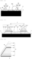
- FIG. 14 is a plane view.
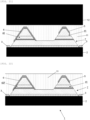
- FIG. 15 is a schematic cross-sectional view along line XV-XV' of the structure shown in FIG. 14 .
- FIG. 16 is a schematic cross-sectional view along line XVI-XVI' of the structure shown in FIG. 14 .
- FIG. 17 is a projection view from XVII direction of the structure shown in FIG. 14 .
- FIG. 18 is an enlarged view of XVIII portion of the structure shown in FIG. 15 .
- FIG. 19 is an enlarged view of XIX portion of the structure shown in FIG. 16 .
- a first conductivity-type GaAs buffer layer (not shown) is laminated, then an AlAs sacrificial layer 41A, a first conductivity-type AlGaInP first cladding layer 41B, a non-doped AlGaInP active layer 41C, a second conductivity-type AlGaInP second cladding layer 41D, a second conductivity-type GaInP intermediate layer (not shown), and a second conductivity-type GaP window layer 41E are epitaxially grown in sequence. Composition and thickness of each layer are as described above. Consequently, the first structure 41 can be obtained as shown in FIGs. 14, 15 , 17 and 18 .
- each of the epitaxial layers (a sacrificial layer 42A, a first cladding layer 42B, an active layer 42C, a second cladding layer 42D, an intermediate layer (not shown), and a window layer 42E) is also epitaxially grown in sequence. Consequently, the stacked portion 42F can be obtained as shown in FIGs. 14, 15 , and 17 .
- a sacrificial layer 43A and a stacked portion 43F are also epitaxially grown in sequence. Consequently, the bridge portion 43 can be obtained as shown in FIGs. 14 , 16 , 17 , and 19 .
- ⁇ 111 ⁇ planes 4A with slow growth speed appear along with a growth of (001) planes by set a V/III ratio as 50 or less; thus, the epitaxial layer structure 4 in pyramid-shape or truncated pyramid-shape can be formed.
- the V/III ratio is more preferably 10 or more.
- the first structure 41 and the stacked portion 42F can be obtained as the epitaxial layer structures in the truncated pyramid shape, as shown in FIGs. 14, 15 , and 17 .
- a total thickness of the first structure 41 in a direction perpendicular to a surface of the starting substrate 2 is Lh.
- T is a sum of the thicknesses of each of the first structure 41 and the stacked portion 42F of epitaxial layer structure 4, up to each of the active layer 41C and the active layer 42C, in a direction perpendicular to the surface of the starting substrate 2.
- the bridge portion 43 can be obtained as the epitaxial layer structures in the truncated pyramid shape, as shown in FIGs. 14 , 16, and 17 .
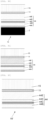
- FIG. 18 shows an enlarged view in the vicinity of the ⁇ 111 ⁇ plane (slope) 4A portion of the first structure 41 which is the light-emitting device portion.
- the stacked portion 42F of the second structure 42 as the non-light-emitting device portion, is similar because the size is the same.
- the width of the opening 31 to expose each of the region 21 for forming the first structure 41 and the region for forming the stacked portion 42F of the region 22 for forming the second structure 42 is set in advance so as to enable all epitaxial layers up to each of window layers 41E and 42E to be stacked in accordance with designed thickness in the [001] direction, and thus the epitaxial layers are grown in such a way.
- the ⁇ 111 ⁇ planes 4A as the slopes, have a stacked structure of the same kind and the same sequence with the [001] direction, as shown in FIG. 18 ; however, the growth speed of the ⁇ 111 ⁇ planes is less than one-fiftieth of that of the (001) planes when the V/III ratio is 50 or less; for example, when the V/III ratio is set to 30, the layer in the slope direction becomes an ultra-thin layer and fully depleted.
- FIG. 18 shows as if layers from the active layer to the window layer have a certain thickness, but this is for the sake of convenience.
- the ⁇ 111 ⁇ plane 4A which is the slope of the laminate portion 43F, includes layers (the sacrificial layer 43A, the first cladding layer 43B, the active layer 43C, the second cladding layer 43D, the intermediate layer (not shown) and the window layer 43E) containing each of all materials of the epitaxial layers included in the first structure 41 (the sacrificial layer 41A, the first cladding layer 41B, the active layer 41C, the second cladding layer 41D, the intermediate layer (not shown) and the window layer 41E); however, by designing the opening width W in advance so as to make the apex of the pyramid-shape of the stacked portion 43F to reach above the first cladding layer 43B, the layers above the active layer 43C are thin films because only ⁇ 111 ⁇ planes are grown, and this is a difference from the structure shown in FIG. 19
- an electrode made of a material that forms ohmic to a second conductivity-type semiconductor is formed on the GaP window layer 41E portion of the first structure 41 which is the light-emitting device portion.
- An electrode made of a material that forms ohmic to a first conductivity-type semiconductor is formed on the second structure 42 which is the non-light-emitting device portion.
- the electrodes thus formed are the electrodes 5 and 6 shown in FIGS. 1 and 2 . With regard to the details of the electrodes 5 and 6, the previous description should be referred.
- the electrodes of different polarity are thus formed on the first structure 41 and the second structure 42, respectively, to manufacture a wafer 1 having a micro-LED structure 7 operable as one micro-LED, which is constituted by the first structure 41 and the second structure 42, shown in FIGs. 1 and 2 . That is, according to the manufacturing method described above, the inventive wafer 1 having a micro-LED structure 7 can be manufactured.
- the inventive wafer 1 having a micro-LED structure 7 can have a variety of modifications, and a design change can be performed by simply changing, for example, a size and a design of the mask pattern of the mask 3.
- wafer 1 without a mask can be obtained by, for example, manufacturing the wafer 1 having a micro-LED structure 7 according to the method described above, then forming a resist mask or a hard mask on a portion other than the mask 3 by photolithography and removing the mask 3 according to an appropriate method.
- FIGs. 20 to 27 an example of the inventive method for manufacturing a bonded semiconductor wafer having a micro-LED structure is described.
- a wafer 1 having a micro-LED structure 7, shown in FIGs. 1 and 2 is manufactured according to the method described earlier with reference to FIGs. 12 to 19 .
- a surface where the micro-LED structure 7 of the wafer 1 is formed is coated with, for example, benzocyclobutene (BCB) of about 0.6 um as a bonding material 11.
- BCB benzocyclobutene
- the thickness of BCB is not limited to this condition, and the same effect can be obtained with a thicker or thinner thickness.
- the bonding material 11 is not limited to BCB and other bonding material may be used.
- a substrate 12 for flattening treatment is pressed against the layer of the bonding material 11 to perform flattening treatment.
- pressuring treatment may be performed with heating up to a range to a temperature (150°C) in which BCB is not cured.
- the flattening treatment substrate 12 is removed as shown in Fig. 22 , and BCB curing treatment is performed by, for example, maintaining the temperature at 250°C for 1 hour.
- ICP dry etching treatment is performed with fluorine-based plasma.
- the coating of BCB is performed under a condition of the BCB thickness of 0.6 um, and then the flattening treatment is performed; thus, by performing the dry etching under a condition equivalent to an etching condition of 0.1 um for a flat plate, the BCB, which coats the apexes of the first structure 41 and stacked portion 42F each of which is the pyramidal shape portion, is etched to expose the electrodes 5 and 6, as shown in FIG. 23 .
- the resist mask or the hard mask is formed by photolithography, and then BCB (bonding material ) 11 in a region where the devices are to be isolated from each other is removed by fluorine-based plasma to form the substrate 13 for device-isolation processing, as shown in FIG. 24 .
- BCB bonding material
- an adhesive layer 14 such as a silicone adhesive layer, is formed on one of the main surfaces of a support substrate 15, such as a quartz substrate.
- the silicone adhesive layer 14 is then adhesively bonded to the exposed surfaces of the electrodes 5 and 6 of the substrate 13 for device-isolation processing to obtain a bonded substrate 16, as shown in FIG. 25 .
- At least sacrificial layers 41A, 42A, and 43A of the bonded substrate 16 are immersed in HF, and a sacrificial layer etching is performed, as shown in FIG. 26 , to separate the start substrate 2.
- a bonded semiconductor wafer 100 having a micro-LED structure 7 shown in FIG. 27 is manufactured.
- the process for the device isolation or the process such as the electrode-formation process to the micro-LED structure 7 is unnecessary.
- the micro-LED 7, in which brightness decrease due to damage originated by the processing is suppressed can be provided.
- Example 1 a wafer having a micro-LED structure was manufactured by following procedures.
- a mask 3 of SiO 2 having a mask pattern including an opening 31 was formed on an N-type GaAs starting substrate 2 to obtain a patterned substrate 2.
- a portion corresponding to a region 21 for forming a first structure 41 was made to have rectangular planar shape
- a portion corresponding to a region 22 for forming a second structure 42 was made to have a region where all corners were at right angles (90°)
- each side of the opening 31 was arranged almost parallel or perpendicular to a [100] direction.
- an n-type GaAs buffer layer (not shown) having a thickness of 0.5 um is stacked, and then a first conductivity-type AlAs sacrificial layer 41A having a thickness of 0.5 um, a first conductivity-type (Al y Ga 1-y ) x In 1-x P (x:0.5; y:0.85) first cladding layer 41B having a thickness of 1.0 um, a non-doped (Al y Ga 1-y ) x In 1-x P (x:0.5; y:0.1) active layer 41C having a thickness of 0.25 um, a second conductivity-type (Al y Ga 1-y ) x In 1-x P (x:0.5; y:0.85) second cladding layer 41D having a thickness of 0.75 um, a second conductivity-type GaInP intermediate layer (not shown) having a thickness of 0.1 um, and
- each epitaxial layer (a sacrificial layer 42A, a first cladding layer 42B, an active layer 42C, a second cladding layer 42D, an intermediate layer (not shown) and a window layer 42E) was epitaxially grown sequentially.
- the stacked portion 42F shown in FIGs. 14, 15 , 17 and 18 was obtained.
- a sacrificial layer 43A and a stacked portion 43F were epitaxially grown sequentially.
- the bridge portion 43 shown in FIGs. 14 , 16 , 17 and 19 was obtained.
- a metal including Au as a main material and Ge was used.
- a P-type electrode 5 was formed only on the P-type GaP window layer 41E of the first structure 41.
- a metal including Au as the main material and Be was used.
- a wafer 1 having a micro-LED structure 7 shown in FIGs. 1 and 2 was obtained.
- a bonded semiconductor substrate having a micro-LED structure was manufactured in a following procedure.
- BCB as a bonding material 11
- a substrate 12 for flattenining treatment was pressed to the material 11 with a pressure of 10 N/cm 2 at room temperature to perform a flattening treatment as shown in FIG. 21 .
- the wafer was kept at 250°C for 1 hour to perform BCB curing treatment, resulting in a state shown in FIG. 22 .
- ICP dry etching treatment with fluorine-based plasma was performed under a condition equivalent to an etching condition of 0.1 um on a flat plate.
- BCB at the apexes of the first structure 41 and the laminate portion 42F in pyramidal-shape portions were etched to expose the electrodes 5 and 6 as shown in FIG. 23 .
- a resist mask or a hard mask was formed by photolithography, and BCB in a region where the devices are to be isolated from each other was removed by fluorine-based plasma to form a substrate 13 for device-isolation processing, as shown in FIG. 24 .
- a silicone adhesive layer 14 was formed on one of main surfaces of a quartz substrate which was a support substrate 15, and the silicone adhesive layer 14 was adhesively bonded to a surface of the substrate 13 for device-isolation processing where the electrodes 5 and 6 were exposed to obtain a bonded substrate 16 shown in FIG. 25 .
- the substrate 16 was immersed in HF and sacrificial layer etching was performed to separate the starting substrate 2, as shown in FIG. 26 .
- a bonded semiconductor wafer 100 having a micro-LED structure 7 shown in FIG. 27 was manufactured.
- Comparative Example a bonded semiconductor wafer was manufactured in a following procedure described with reference to FIGs. 28 to 35 .
- an N-type GaAs buffer layer (not shown) having a thickness of 0.5 um was stacked on an N-type GaAs substrate 2 which has no mask pattern, and then an N-type Ga x In 1-x P (x:0.5) first sacrificial layer having a thickness of 0.3 um and an N-type GaAs second sacrificial layer having a thickness of 0.3 um were epitaxially grown to make a sacrificial layer 44A; on this sacrificial layer 44A, an N-type (Al y Ga 1-y ) x In 1-x P (x:0.5; y:0.85) first cladding layer 44B having a thickness of 1.0 um, a non-doped (Al y Ga 1-y ) x In 1-x P (x:0.5; y:0.1) active layer 44C having a thickness of 0.25 um, a P-type (Al y Ga 1-y ) x In 1-x P (x:0.5;
- BCB benzocyclobutene
- the GaAs starting substrate 2 was removed by wet etching to expose the first sacrificial layer as shown in FIG. 31 , and then an etchant was switched and the sacrificial layer 44A made up of the first sacrificial layer and the second sacrificial layer, respectively, were removed to expose the first cladding layer 44B, thereby producing an epitaxial (EP) bonded substrate 16' shown in FIG. 32 .
- EP epitaxial
- a mask was formed on the EP bonded substrate 16' (lower side in the drawing) by a photolithography method, and then a part of each of the layers from the first cladding layer 44B to the GaP window layer 44E was etched.
- a device-isolation step to form an island-shaped devices and an etching step to expose a part of the second cladding layer 44D were performed. Owing to these steps, a plurality of island-shaped devices 45 shown in FIG. 33 was obtained.
- a passivation (PSV) film 9 made of SiO 2 was formed on a surface of the island-shaped device 45.
- the PSV film 9 was formed using a TEOS+O 2 -based P-CVD apparatus and a film thickness was set to 0.4 um.
- the PSV 9 was processed so as to expose a part of each of the first cladding layer 44B and the second cladding layer 44D as shown in FIG. 34 .
- each of electrodes 5 and 6 was formed on a part of each of the first cladding layer 44B and the second cladding layer 44D exposed through an opening of the PSV film 9, then heat treatment was performed to realize an ohmic contact.
- the electrodes 5 and 6 in this regard were the same as in Example.
- Example 1 a size of one side of the first structure 41, which was a light-emitting device portion, was changed from 10 to 250 um to manufacture a plurality of bonded semiconductor wafers 100.
- a size of one side of the island-shaped device 45 was changed from 10 to 250 um to manufacture a plurality of bonded semiconductor wafers 200.
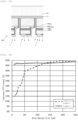
- FIG. 36 shows a relation between the size of one side (dice design size) of the first structure 41 or the island-shaped device 45, which are the light-emitting device portions, and external quantum efficiency (luminous efficiency) at a current density of 8 [A/cm 2 ] for Example 1 and Comparative Example.
- the dice design size corresponded to a length of one side of the opening (in square) for the light-emitting device portion of a mask pattern in a mask 3.
- the current was changed so as to maintain the current density at 8 A/cm 2 .
- Luminous efficiency was calculated by optical output [W] / input power [W].
- the luminous efficiency significantly decreases as the size of the island-shaped device 45, which is the light-emitting device, decreases. This is considered to be caused by damage inflicted on the light-emitting device portion due to device-isolation processing and subsequent device processing.
- Example 1 even when the size of the first structure 41 is smaller than 100 um or less, which is a size of a typical micro-LED level, a significant luminous efficiency decrease does not occur.
- the inventive wafer 1 having a micro-LED structure 7 device processing after epitaxial growth is not required in principle; thus, no cross-section generated by processing is present.
- outer surfaces of an epitaxial layer structure 4 are constituted solely by an epitaxial surface. Therefore, the first structure 41, which is the light-emitting device portion, has no damage due to processing.
- the inventive wafer 1 having a micro-LED structure 7 has no processing damage, resulting in no need for a damage-removing step.
- the surface is coated with a thin film portion of the window layer 41E which also has an effect similar to a passivation layer; even when a passivation film is not formed, a surface state reduction effect is exhibited in a similar way in which the passivation layer is formed; therefore, a photon absorbed by the surface state is decreased, resulting in suppressing decrease in luminous efficiency compared to a conventional art.
Landscapes
- Led Devices (AREA)
Abstract
Description
- The present invention relates to a wafer having a micro-LED structure, a method for manufacturing a wafer having a micro-LED structure, and a method for manufacturing a bonded semiconductor wafer having a micro-LED structure.
- A technique to separate parts necessary to function as light-emitting devices (hereinafter, referred to as functional layers) out of laminates epitaxially grown on starting substrates (hereinafter referred to as epitaxial layer structures) from starting substrates and transfer the parts to another substrate is an important technique to mitigate restriction due to physical properties of the starting substrates and to increase the degree of freedom in designing device systems.
- Concerning micro-LED devices, transferring the devices staying on the starting substrates to a drive circuit is difficult, and a transferring technique to transfer functional layers to appropriate substrates is indispensable. To produce a donor substrate capable of performing the transferring to the drive circuit suitable for the micro-LED device, the technique to realize the transferring is necessary in which the functional layer is bonded to a permanent substrate to obtain a bonded substrate and then the starting substrate is removed from this bonded substrate, or the starting substrate is removed while the function layer being held by a temporary support substrate and then the function layer is bonded to the permanent substrate, and the like.
- In addition, when the function layer is epitaxially grown on the entire wafer, and an obtained epitaxial layer is device-isolated by etching processing to provide a desired micro-LED size, etching damage is generated at a processed interface, which causes a brightness decrease. In the micro-LED with a small device size, it is problematic that the brightness decrease due to this etching damage is significant.
-
Patent Document 1 discloses a technique for thermo-compressionally bonding a semiconductor epitaxial substrate to a temporary supporting substrate via a dielectric layer and a technique for separating a temporary supporting substrate and an epitaxial functional layer by wet etching. In addition,Patent Document 2 discloses a technique in which a sacrificial layer and a semiconductor crystal layer are formed on a single crystal layer of a starting substrate in this order, and an isolation groove is formed to the semiconductor crystal layer to expose the sacrificial layer, and then the semiconductor crystal layer is bonded to a transfer substrate, and then sacrificial-layer etching is performed via the isolation groove, thereby separating the starting substrate. - Manufacturing of a micro-LED having a miniaturized light-emitting device portion can be realized using these techniques; however, no improvement measures toward the brightness decrease have not been presented.
-
- Patent Document 1:
JP 2021-27301 A - Patent Document 2:
WO 2014-020906 A1 - The present invention has been made in view of the above-described problem. An object of the present invention is to provide a wafer having a micro-LED structure in which generation of a brightness decrease is suppressed; a method for manufacturing the wafer having a micro-LED structure in which generation of a brightness decrease is suppressed; and a method for manufacturing a bonded semiconductor wafer having a micro-LED structure in which generation of a brightness decrease is suppressed.
- To achieve the object, the present invention provides a wafer having a micro-LED structure, the wafer comprising:
- a starting substrate;
- a mask formed on the starting substrate and having a mask pattern including an opening; and
- a plurality of epitaxial layer structures, each of the plurality of structures selectively grown on a portion corresponding to the opening of the mask pattern on the starting substrate,
- wherein each of the plurality of the epitaxial layer structures has a pyramid-shape or a truncated pyramid-shape surrounded by {111} planes,
- the plurality of epitaxial layer structures includes a first structure, as a light-emitting device portion, and a second structure connected to the first structure, and
- a polarity of an electrode of the first structure is different from that of an electrode of the second structure, and the first structure and the second structure constitute a micro-LED structure operable as one micro-LED.
- In the inventive wafer having a micro-LED structure, the micro-LED structure constituted on the wafer is constituted by the first structure and the second structure of the epitaxial layer structures selectively grown in a state separated by the mask in advance; thus, device-isolation processing is not necessary; in addition, since the polarity of the electrode of the first structure is different from that of the electrode of the second structure, one of the electrodes can make contact with an N-type electrode and the other of the electrodes can make contact with a P-type electrode, resulting in eliminating a need for processing such as dry etching of the epitaxial layer structure to form electrodes. Consequently, the inventive wafer having a micro-LED structure can provide the micro-LED structure, in which brightness decrease due to damage originated by the processing such as the device-isolation processing and electrode-forming processing is suppressed. With a transfer of the micro-LED structure from the inventive wafer having a micro-LED structure to a substrate suitable for a micro-LED device, the micro-LED device having the micro-LED structure with excellent brightness can be produced.
- It is preferred that the plurality of the epitaxial layer structures have thin films which are full depletion layers in {111} plane directions.
- By including such a plurality of epitaxial layer structures, an insulating property between the electrodes can be secured.
- It is preferred that the first structure is the light-emitting device portion having an AlGaInP-based light-emitting layer and Lh ≤ 0.707 × Lws where a width of a shortest portion at a bottom is Lws, and a total thickness of the first structure in a direction perpendicular to a surface of the starting substrate is Lh.
- In the first structure having such a configuration, all epitaxial layers necessary to function as the light-emitting device portion can be made to grow in accordance with the design thickness in the [001] direction perpendicular to the starting substrate surface.
- The width Lws of the shortest portion at the bottom of the first structure may be 10 um or more and 100 um or less.
- According to the inventive wafer having a micro-LED structure, even when the micro-LED structure has the width Lws of the shortest portion of the bottom of the first structure with 10 um or more and 100 um or less, the generation of brightness decrease can be sufficiently suppressed.
- It is preferred that the epitaxial layer structure includes an active layer, and the second structure is a non-light-emitting device portion and includes a pyramid-shape bridge portion at least partially, and 1.5 um < W < T/0.707 where a width of a shortest part of the bridge portion is W [pm] and a sum of thicknesses of the epitaxial layer structure up to the active layer in the direction perpendicular to the surface of the starting substrate is T [um].
- When a lower layer below the active layer is made to be the first conductivity-type and an upper layer is made to be the second conductivity-type, and by satisfying W < T/0.707, a bridge portion of the second structure can be pyramid-shape having no flat portion before reaching the second conductivity-type layer. In addition, when W > 1.5 um, a thickness of a first conductivity-type cladding layer necessary to make contact with a first conductivity-type electrode can be ensured.
- In addition, the present invention provides a wafer having a micro-LED structure, the wafer comprising:
- a starting substrate; and
- a plurality of epitaxial layer structures each of which is selectively grown on a portion of the starting substrate,
- wherein each of the plurality of the epitaxial layer structures has a pyramid-shape or a truncated pyramid-shape surrounded by {111} planes,
- the plurality of epitaxial layer structures includes a first structure, as a light-emitting device portion, and a second structure connected to the first structure, and
- a polarity of an electrode of the first structure is different from that of an electrode of the second structure, and the first structure and the second structure constitute a micro-LED structure operable as one micro-LED.
- The wafer having a micro-LED structure according to another aspect of the present invention may not have a mask. In the wafer having a micro-LED structure according to this aspect, since the micro-LED structure constituted on the wafer is constituted by the first structure and the second structure of epitaxial layer structures, each of which is selectively grown, device-isolation processing is not necessary. In addition, the polarity of the electrode of the first structure is different from that of the electrode of the second structure. Thus, one of the electrodes can make contact with an N-type electrode and the other of the electrodes can make contact with a P-type electrode, resulting in eliminating a need for processing, such as dry etching, to the epitaxial layer structure to form the electrodes. Consequently, the wafer having a micro-LED structure according to this aspect can provide the micro-LED structure, in which brightness decrease due to damage originated by the processing such as the device-isolation processing and the electrode-forming processing is suppressed. By a transfer of the micro-LED structure from the wafer having a micro-LED structure according to such an aspect to a substrate suitable for the micro-LED device, the micro-LED device can be produced in which the micro-LED structure that shows excellent brightness is provided.
- Moreover, the present invention provides a method for manufacturing a wafer having a micro-LED structure, the method comprising:
- providing a starting substrate;
- forming a mask having a mask pattern including an opening on the starting substrate;
- selectively growing a plurality of epitaxial layer structures, including a first structure as a light-emitting device portion and a second structure connected to the first structure, on a portion exposed through the opening of the mask pattern on the starting substrate, such that each of the plurality of the epitaxial layer structures has a pyramid-shape or a truncated pyramid-shape surrounded by {111} planes; and
- forming electrodes of different polarities to the first structure and the second structure, respectively, to manufacture a wafer having a micro-LED structure including the first structure and the second structure and operable as one micro-LED.
- The wafer having a micro-LED structure manufactured by such a manufacturing method has the micro-LED structure constituted by the first structure and the second structure of the epitaxial layer structures selectively grown in a state separated by the mask in advance. Such a micro-LED structure has no need for device-isolation processing. In addition, since the polarity of the electrode of the first structure is different from that of the electrode of the second structure, one of the electrode can make contact with an N-type electrode and the other of the electrodes can make contact with a P-type electrode, resulting in eliminating a need for processing to form the electrodes. Consequently, according to the inventive method for manufacturing the wafer having a micro-LED structure, the wafer having a micro-LED structure can be manufactured, in which brightness decrease due to damage originated by the processing such as the device-isolation processing and the electrode-forming processing is suppressed.
- Furthermore, the present invention provides a method for manufacturing a bonded semiconductor wafer having a micro-LED structure, the method comprising:
- manufacturing a wafer having a micro-LED structure by the inventive method for manufacturing the wafer having a micro-LED structure;
- bonding a surface of the wafer where the micro-LED structure is formed to one of main surfaces of a support substrate via a bonding material to obtain a bonded substrate; and
- removing the starting substrate from the bonded substrate to manufacture a bonded semiconductor wafer having the micro-LED structure.
- According to the inventive method for manufacturing the bonded semiconductor wafer having a micro-LED structure, the wafer having a micro-LED structure is manufactured in accordance with the inventive method for manufacturing the inventive wafer having a micro-LED structure and used for manufacturing the bonded semiconductor wafer. Thus, the bonded semiconductor wafer can be manufactured, the bonded semiconductor wafer having a micro-LED structure, in which brightness decrease due to damage originated by the processing such as the device-isolation processing and the electrode-forming processing is suppressed.
- As described above, according to the inventive wafer having a micro-LED structure, it is possible to have the micro-LED structure, in which brightness decrease due to damage originated by the processing such as the device-isolation processing and the electrode-forming processing is suppressed. In addition, with a transfer of the micro-LED structure from the inventive wafer having a micro-LED structure to a substrate suitable for a micro-LED device, the micro-LED device having the micro-LED structure that exhibits excellent brightness can be produced.
- In addition, according to the inventive method for manufacturing the wafer having a micro-LED structure, the wafer having a micro-LED structure, in which brightness decrease due to damage originated by the processing such as the device-isolation processing and the electrode-forming processing is suppressed, can be manufactured.
- Moreover, according to the inventive method for manufacturing the bonded semiconductor wafer having a micro-LED structure, the bonded semiconductor wafer having a micro-LED structure, in which brightness decrease due to damage originated by the processing such as the device-isolation processing and the electrode-forming processing is suppressed, can be manufactured.
-
-
FIG. 1 is a schematic plane view illustrating an example of a wafer having a micro-LED structure according to the present invention. -
FIG. 2 is a projection view illustrating of the wafer having the micro-LED structure shown inFIG. 1 from II direction. -
FIG. 3 is a schematic plane view illustrating another example of the wafer having a micro-LED structure according to the present invention. -
FIG. 4 is a projection view illustrating the wafer having the micro-LED structure shown inFIG. 3 from IV direction. -
FIG. 5 is a schematic plane view illustrating another example of the wafer having a micro-LED structure according to the present invention. -
FIG. 6 is a projection view illustrating the wafer having the micro-LED structure shown inFIG. 5 from a VI direction. -
FIG. 7 is a schematic plane view illustrating another example of the wafer having a micro-LED structure according to the present invention. -
FIG. 8 is a projection view illustrating the wafer having the micro-LED structure shown inFIG. 7 from VIII direction. -
FIG. 9 is a schematic plane view illustrating another example of the wafer having a micro-LED structure according to the present invention. -
FIG. 10 is a projection view illustrating the wafer having the micro-LED structure shown inFIG. 9 from X direction. -
FIG. 11 is a schematic plane view illustrating another example of the wafer having a micro-LED structure according to the present invention. -
FIG. 12 is a schematic plane view illustrating a step in an example of a method for manufacturing the wafer having the micro-LED structure according to the present invention. -
FIG. 13 is a schematic cross-sectional view along line XIII-XIII' of the structure shown inFIG. 12 . -
FIG. 14 is a schematic plane view illustrating a step in an example of the method for manufacturing the wafer having a micro-LED structure according to the present invention. -
FIG. 15 is a schematic cross-sectional view along line XV-XV' of the structure shown inFIG. 14 . -
FIG. 16 is a schematic cross-sectional view along line XVI-XVI' of the structure shown inFIG. 14 . -
FIG. 17 is a projection view from XVII direction of the structure shown inFIG. 14 . -
FIG. 18 is an enlarged view of XVIII portion of the structure shown inFIG. 15 . -
FIG. 19 is an enlarged view of XIX portion of the structure shown inFIG. 16 . -
FIG. 20 is a schematic view illustrating a step in an example of a method for manufacturing a bonded semiconductor wafer having a micro-LED structure according to the present invention. -
FIG. 21 is a schematic view illustrating a step in an example of the method for manufacturing the bonded semiconductor wafer having a micro-LED structure according to the present invention. -
FIG. 22 is a schematic view illustrating a step in an example of the method for manufacturing the bonded semiconductor wafer having a micro-LED structure according to the present invention. -
FIG. 23 is a schematic view illustrating a step in an example of the method for manufacturing the bonded semiconductor wafer having a micro-LED structure according to the present invention. -
FIG. 24 is a schematic view illustrating a step in an example of the method for manufacturing the bonded semiconductor wafer having a micro-LED structure according to the present invention. -
FIG. 25 is a schematic view illustrating a step in an example of the method for manufacturing the bonded semiconductor wafer having a micro-LED structure according to the present invention. -
FIG. 26 is a schematic view illustrating a step in an example of the method for manufacturing the bonded semiconductor wafer having a micro-LED structure according to the present invention. -
FIG. 27 is a schematic view illustrating the bonded semiconductor wafer manufactured by an example of the method for manufacturing the bonded semiconductor wafer having a micro-LED structure according to the present invention. -
FIG. 28 is a schematic cross-sectional view illustrating a step in an example of a method for manufacturing a bonded semiconductor wafer in Comparative Example. -
FIG. 29 is a schematic cross-sectional view illustrating a step in an example of the method for manufacturing the bonded semiconductor wafer in Comparative Example. -
FIG. 30 is a schematic cross-sectional view illustrating a step in an example of the method for manufacturing the bonded semiconductor wafer in Comparative Example. -
FIG. 31 is a schematic cross-sectional view illustrating a step in an example of the method for manufacturing the bonded semiconductor wafer in Comparative Example. -
FIG. 32 is a schematic cross-sectional view illustrating a step in an example of the method for manufacturing the bonded semiconductor wafer in Comparative Example. -
FIG. 33 is a schematic cross-sectional view illustrating a step in an example of the method for manufacturing the bonded semiconductor wafer in Comparative Example. -
FIG. 34 is a schematic cross-sectional view illustrating a step in an example of the method for manufacturing the bonded semiconductor wafer in Comparative Example. -
FIG. 35 is a schematic cross-sectional view illustrating a step in an example of the method for manufacturing the bonded semiconductor wafer in Comparative Example. -
FIG. 36 is a graph illustrating a relation between a dice design size and luminous efficiency of micro-LEDs produced in each of Example and Comparative Example. - As described above, development has been required with regard to a wafer having a micro-LED structure in which generation of a brightness decrease is suppressed; a method for manufacturing the wafer having a micro-LED structure in which generation of a brightness decrease is suppressed; and a method for manufacturing a bonded semiconductor wafer having a micro-LED structure in which generation of a brightness decrease is suppressed.
- The present inventor focuses on the fact that while an epitaxial layer structure, which is to be a micro-LED structure, is epitaxially grown to an opening of a mask pattern provided on a starting substrate, by making a V/III ratio of raw materials to 1 or more and 50 or less, {111} planes with slow growth speed appear along with a growth of a (001) plane parallel to a surface of a starting substrate, resulting in the epitaxial layer structure capable of forming pyramid-shape or truncated pyramid-shape. In addition, the present inventor focuses on the fact that a thickness of the layer of a slope becomes significantly thin compared with a thickness in a direction perpendicular to the surface of the substrate (hereinafter, [001] direction) in such a shapes and thus full depletion of unneeded layers is possible by adjusting a size of the opening and the V/III ratio of the raw materials. The present inventor has earnestly studied on such steps and found that a pair of the epitaxial layer structures in the pyramid-shape or the truncated pyramid-shape, each selectively grown, can be used as the micro-LED structure without processing for device-separation or electrode formation. This finding has led to the completion of the present invention.
- That is, the present invention is a wafer having a micro-LED structure, the wafer comprising:
- a starting substrate;
- a mask formed on the starting substrate and having a mask pattern including an opening; and
- a plurality of epitaxial layer structures, each of the plurality of structures selectively grown on a portion corresponding to the opening of the mask pattern on the starting substrate,
- wherein each of the plurality of the epitaxial layer structures has a pyramid-shape or a truncated pyramid-shape surrounded by {111} planes,
- the plurality of epitaxial layer structures includes a first structure, as a light-emitting device portion, and a second structure connected to the first structure, and
- a polarity of an electrode of the first structure is different from that of an electrode of the second structure, and the first structure and the second structure constitute a micro-LED structure operable as one micro-LED.
- In addition, the present invention is a wafer having a micro-LED structure, the wafer comprising:
- a starting substrate; and
- a plurality of epitaxial layer structures each of which selectively grown on a portion of the starting substrate,
- wherein each of the plurality of the epitaxial layer structures has a pyramid-shape or a truncated pyramid-shape surrounded by {111} planes,
- the plurality of epitaxial layer structures includes a first structure, as a light-emitting device portion, and a second structure connected to the first structure, and
- a polarity of an electrode of the first structure is different from that of an electrode of the second structure, and the first structure and the second structure constitute a micro-LED structure operable as one micro-LED.
- Moreover, the present invention is a method for manufacturing a wafer having a micro-LED structure, the method comprising:
- providing a starting substrate;
- forming a mask having a mask pattern including an opening on the starting substrate;
- selectively growing a plurality of epitaxial layer structures, including a first structure as a light-emitting device portion and a second structure connected to the first structure, on a portion exposed through the opening of the mask pattern on the starting substrate, such that each of the plurality of the epitaxial layer structures has a pyramid-shape or a truncated pyramid-shape surrounded by {111} planes; and
- forming electrodes of different polarities to the first structure and the second structure, respectively, to manufacture a wafer having a micro-LED structure including the first structure and the second structure and operable as one micro-LED.
- Furthermore, the present invention is a method for manufacturing a bonded semiconductor wafer having a micro-LED structure, the method comprising:
- manufacturing a wafer having a micro-LED structure by the inventive method for manufacturing the wafer having a micro-LED structure;
- bonding a surface of the wafer where the micro-LED structure is formed to one of main surfaces of a support substrate via a bonding material to obtain a bonded substrate; and
- removing the starting substrate from the bonded substrate to manufacture a bonded semiconductor wafer having the micro-LED structure.
- Hereinafter, the present invention will be described in detail with reference to the drawings. However, the present invention is not limited thereto.
- The first embodiment of the inventive wafer having a micro-LED structure is schematically shown in
FIGs. 1 and 2. FIG. 1 is a plane view, andFIG. 2 is a projection view (side view) ofFIG. 1 from a II direction. - The
wafer 1 having a micro-LED structure shown inFIGs. 1 and 2 includes a startingsubstrate 2, amask 3 formed on this startingsubstrate 2 with a mask pattern including an opening (not shown inFIG. 1 and FIG. 2 ), and a plurality ofepitaxial layer structures 4 each of which selectively grown on a portion corresponding to the opening of the mask pattern on the starting substrate 2 (not shown inFIGs. 1 and 2 ). - Each of the plurality of the
epitaxial layer structures 4 has a pyramid-shape or a truncated pyramid-shape surrounded by {111}planes 4A. - The plurality of the
epitaxial layer structures 4 includes afirst structure 41, as a light-emitting device portion, and asecond structure 42 connected to thefirst structure 41. - The
first structure 41 includes anelectrode 5. Thesecond structure 42 includes anelectrode 6. Theelectrodes first structure 41 and thesecond structure 42 constitute amicro-LED structure 7 operable as one micro-LED. - In the
wafer 1 having such amicro-LED structure 7, themicro-LED structure 7 constituted on thewafer 1 is constituted by thefirst structure 41 and thesecond structure 42 of theepitaxial layer structures 4 each of which selectively grown in a state separated by themask 3 in advance; thus, device-isolation processing is not necessary. In addition, since the polarity of theelectrode 5 of thefirst structure 41 is different from that of theelectrode 6 of thesecond structure 42, and one of the electrodes can make contact with an N-type electrode and the other of the electrodes can make contact with a P-type electrode, resulting in eliminating a need for processing such as dry etching of the epitaxial layer structure to form electrodes. Consequently, thewafer 1 having amicro-LED structure 7 shown inFIGs. 1 and 2 can provide themicro-LED structure 7, in which brightness decrease due to damage originated by the processing such as the device-isolation processing and an electrode-forming processing is suppressed. In addition, with a transfer of themicro-LED structure 7 from thewafer 1 having such amicro-LED structure 7 to a substrate suitable for a micro-LED device, the micro-LED device can be produced in which themicro-LED structure 7 that shows excellent brightness is provided. - Hereinafter, the
wafer 1 having amicro-LED structure 7 of the first embodiments shown inFIGs. 1 and 2 is described in more detail. - As the starting
substrate 2, for example, a first conductivity-type GaAs substrate can be used without limitation. The startingsubstrate 2 may have a buffer layer (not shown), for example, a first conductivity-type GaAs buffer layer on a surface thereof. In the first embodiment shown inFIGs. 1 and 2 , the GaAs buffer layer typically has a thickness of 0.5 µm. - The
mask 3 forms, for example, a nonpolar dielectric film such as SiO2 or silicon nitride, and forms the mask pattern made of the nonpolar dielectric film having the openings. Of the openings of the mask pattern, a region where thefirst structure 41 is formed has, for example, a rectangular planar shape. In addition, of the openings of the mask pattern, a region where thesecond structure 42 is formed is, for example, the region having all corners of right angles (90°). The openings of the mask pattern, the region in which thefirst structure 41 is formed and the region in which thesecond structure 42 is formed are described in a description of the inventive method for manufacturing the wafer having a micro-LED structure in a later section with reference to the drawings. - In the first embodiment shown in
FIGs. 1 and 2 , themask 3 includes a portion formed on a portion including a center of the startingsubstrate 2 and a portion formed on an outer edge portion of thesubstrate 2. - The
first structure 41 is the light-emitting device portion having the truncated pyramid-shape (also referred to as a pyramidal shape), in which asacrificial layer 41A, afirst cladding layer 41B, anactive layer 41C, asecond cladding layer 41D, an intermediate layer (not shown), and awindow layer 41E are included in this order. Because thefirst structure 41 is a part of theepitaxial layer structure 4, these layers are the epitaxial layers. - The
sacrificial layer 41A can include, for example, an AlAs sacrificial layer, a GaInP sacrificial layer, and/or a GaAs sacrificial layer. Thesacrificial layer 41A may be constituted by a plurality of layers. In the first embodiment shown inFIGs. 1 and 2 , thesacrificial layer 41A is a first conductivity-type AlAs sacrificial layer having a thickness of 0.5 µm. - The
first cladding layer 41B is, for example, a first conductivity-type AlGaInP (for example, (AlyGa1-y)xIn1-xP (0.4 ≤ x ≤ 0.6, 0 < y ≤ 1)) first cladding layer. In the first embodiment shown inFIGs. 1 and 2 , thefirst cladding layer 41B is the layer having "x" and "y" in the general formula as 0.5 and 0.85, respectively, and a thickness of 1.0 µm. - The
active layer 41C is, for example, a non-doped AlGaInP (for example, (AlyGa1-y)xIn1-xP (0.4 ≤ x ≤ 0.6, 0 ≤ y ≤ 0.6))-based light emitting layer. In the first embodiment shown inFIGs. 1 and 2 , theactive layer 41C is the layer having "x" and "y" in the general formula above as 0.5 and 0.1, respectively, and having a thickness of 0.25 µm. - The
second cladding layer 41D is, for example, a second conductivity-type AlGaInP (for example, (AlyGa1-y)xIn1-xP (0.4 ≤ x ≤ 0.6, 0 < y ≤ 1)) second cladding layer. In the first embodiment shown inFIGs. 1 and 2 , thesecond cladding layer 41D is the layer having "x" and "y" in the general formula above as 0.5 and 0.85, respectively, and a thickness of 0.75um. - The intermediate layer not shown is, for example, a second conductivity-type GaInP intermediate layer, and is the layer having a thickness of 0.1 um in the first embodiment shown in
FIGs. 1 and 2 . - The
window layer 41E is, for example, a second conductivity-type GaP window layer. In the first embodiment shown inFIGs. 1 and 2 , thewindow layer 41E is the layer having a thickness of 1.9 µm. - As shown in
FIG. 1 , a width of a shortest portion at a bottom of thefirst structure 41 is Lws. Even when the width Lws of the shortest portion at the bottom of thefirst structure 41, as the light-emitting device portion, is 10 um or more and 100 um or less, i.e., a typical micro-LED size, theinventive wafer 1 having amicro-LED structure 7 can provide themicro-LED structure 7 in which brightness decrease due to damage originated by the processing is suppressed because the processing such as the device-isolation processing and electrode-forming processing is unnecessary. - In addition, as shown in
FIG. 2 , a total thickness of thefirst structure 41 in a direction perpendicular to a surface of the starting substrate 2 ([001] direction) is Lh. It is preferred that the total thickness Lh of thefirst structure 41 and the width Lws of the shortest portion at the bottom of thefirst structure 41 satisfy Lh ≤ 0.707 × Lws. Thefirst structure 41 having such a structure can be prevented from being a pyramid-shape with no flat portion on an apex before reaching a design thickness, thereby all epitaxial layers necessary to function as the light-emitting device portion can be made to grow in the [001] direction to the design thickness. The lower limit of the total thickness Lh is not particularly limited but is, for example, 0.5 µm. - As shown in
FIGS. 1 and 2 , thesecond structure 42 is connected to thefirst structure 41. More specifically, thesecond structure 42 includes a pyramid-shapedbridge portion 43 at least partially, which is in contact with thefirst structure 41. - The
bridge portion 43 has asacrificial layer 43A integrated with thesacrificial layer 41A of thefirst structure 41, and astacked portion 43F on thelayer 43A. - As shown in
FIG. 18 described later, the stackedportion 43F contains respective materials of the epitaxial layers of thefirst structure 41 but has the pyramid-shape so as to make the apex at a top layer of the first cladding layer. Consequently, only the {111} planes 4A are grown above the active layer, resulting in thin films. That is, thebridge portion 43 has a second conductivity-type layer being fully depleted, thus practically behaving as a first conductivity-type. - The
second structure 42 shown inFIGs. 1 and 2 further includes asacrificial layer 42A, afirst cladding layer 42B, anactive layer 42C, asecond cladding layer 42D, an intermediate layer (not shown), and awindow layer 42E in this order as similar to thefirst structure 41, and these layers constitute astacked portion 42F. Thesacrificial layer 42A is integrated with thesacrificial layers - The
second structure 42 shown inFIGs. 1 and 2 is a non-light-emitting device portion. In addition, as shown inFIG. 1 , a width of a shortest part of thebridge portion 43 is W [pm]. Moreover, a sum of thicknesses of theepitaxial layer structure 4 up to theactive layers substrate 2 is T [pm]. In the first embodiment shown inFIGs. 1 and 2 , then 1.5 um < W < T/0.707. When layers below the active layer are in the first conductivity-type and layers above the active layer are in the second conductivity-type, by satisfying W < T/0.707, abridge portion 43 of thesecond structure 42 can have a pyramid-shape having no flat portion before reaching the second conductivity-type layers. In addition, when W > 1.5 um, a thickness of a first conductivity-type cladding layer necessary to contact a first conductivity-type electrode can be ensured. - It is preferred that a plurality of the epitaxial layer structures 4 (in the first embodiment shown in
FIGs. 1 and 2 , thefirst structure 41, and thesecond structure 42 including the stackedportion 42F and the bridge portion 43) have thin films which are full depletion layers in {111}plane 4A directions. - On the
window layer 41E portion of thefirst structure 41, theelectrode 5 is formed with a material that allows a formation of an ohmic to a second conductivity-type semiconductor. - On the other hand, on the stacked
portion 42F of thesecond structure 42, theelectrode 6 is formed with a material that allows a formation of an ohmic to a first conductivity-type semiconductor. - In the first embodiment shown in
FIGs. 1 and 2 , theelectrode 6 formed on thesecond structure 42 extends from thewindow layer 42E, which is the structural apex of the stackedportion 42F, to thebridge portion 43 and is in ohmic contact with the first conductivity-type bridge portion 43. In this case, a part of theelectrode 6 is in contact with thesecond cladding layer 42D and thewindow layer 42E of thesecond structure 42, which is a non-light-emitting device portion, either directly or through the depletion layer; however, another part of theelectrode 6 is in contact with the first conductivity-type bridge portion 43, thus being short-circuited state and not conducting current through a PiN junction, resulting in no electrical problem. - Since the
bridge portion 43, a part of the plurality of theepitaxial layer structures 4, has thin films which are full depletion layers in {111}plane 4A directions, an insulating property between theelectrodes - Moreover, an outermost periphery of the
bridge portion 43 is covered with fully depleted ultrathin layers, and thus the insulating property between the electrodes is secured; however, when the effective V/III ratio on the surface increases due to a lower growth temperature in the formation process of thebridge portion 43, etc., the layer thickness on the slope may become large, resulting in leakage. In such a case, as in a variant shown inFIGs. 3 and4 (FIG. 3 : a plane view;FIG. 4 : a projection view ofFIG. 3 from a IV direction (side view)), a part of the stackedportion 43F of thebridge portion 43 may be removed by a method such as dry etching for making astacked portion 43G to prevent the leakage. - In addition, in the first embodiment described above, a case is shown in which the height of the
first structure 41, which is the light-emitting device portion, and the height of the stackedportion 42F of thesecond structure 42, which is the non-light-emitting device portion, are even; however, the stackedportion 42F of thesecond structure 42, which is the non-light-emitting device portion, may be lower than thefirst structure 41, which is the light-emitting device portion. Moreover, as in a variant shown inFIGs. 5 and6 , thesecond structure 42, as the non-light-emitting device portion, may only have the bridge portion 43 (FIG. 5 : a plane view;FIG. 6 : a projection view ofFIG. 5 from a VI direction (side view)). Such a design change can be made simply by changing the size and design of the mask pattern of themask 3. On the other hand, the stackedportion 42F of thesecond structure 42, which is the non-light-emitting device portion, can be made higher than thefirst structure 41, which is the light-emitting device portion; however, theportion 42F usually stops growth thereof when theGaP window layer 41E of the light-emitting device portion is stacked until design thickness, thus the non-light-emitting device portion is never higher than the light-emitting device portion, and the non-light-emitting device portion having a large height than that of the light-emitting device portion has no functional merit. Owing to these reasons, it is suitable that the height of the stackedportion 42F of thesecond structure 42, as the non-light-emitting device portion, is lower or equal to the height of thefirst structure 41, as the light-emitting device portion. - The second embodiment of the inventive wafer having a micro-LED structure is schematically shown in
FIGs. 7 and 8. FIG. 7 is a plane view, andFIG. 8 is a projection view (side view) ofFIG. 7 from a VIII direction. - The second embodiment shown in
FIGs. 7 and 8 is the same as the first embodiment except that a shape of afirst structure 41, as a light-emitting device portion, is changed. A rectangular-shaped device can be realized by making a size of thefirst structure 41, as the light-emitting device portion, horizontally long while keeping a size of asecond structure 42, as a non-light-emitting device portion, intact. - The second embodiment of the inventive wafer having a micro-LED structure is schematically shown in
FIGs. 9 and10 .FIG. 9 is a plane view, andFIG. 10 is a projection view (side view) ofFIG. 9 from an X direction. - The third embodiment shown in
FIGs. 9 and10 is the same as the first embodiment except that a shape of afirst structure 41, as a light-emitting device portion, is changed, and, in line with this, a shape of abridge portion 43 of asecond structure 42, which is a non-light-emitting device portion, is changed. By keeping a size of astacked portion 42F of thesecond structure 42, which is the non-light-emitting device portion, intact, and arranging thebridge portion 43 and thefirst structure 41, which is the light-emitting device portion, along two sides of a periphery of the stackedportion 42F, a device having a shape shown inFIGs. 9 and10 is realized. - A wafer having a micro-LED structure according to another aspect of the present invention may not include a mask.
- The fourth embodiment of the inventive wafer having a micro-LED structure is schematically shown in
FIG. 11. FIG. 11 is a plane view. - The fourth embodiment shown in
FIG. 11 is the same as the first embodiment, except that a mask is not included. - More in detail, a
wafer 1 having a micro-LED structure shown inFIG. 11 includes a startingsubstrate 2 and a plurality ofepitaxial layer structures 4 selectively grown onportions substrate 1. Each of the plurality ofepitaxial layer structures 4 is of a pyramid-shape or a truncated pyramid-shape surrounded by {111}planes 4A. The plurality of theepitaxial layer structures 4 includes afirst structure 41, as a light-emitting device portion, and asecond structure 42 connected to thefirst structure 41. Thefirst structure 41 has anelectrode 5 and thesecond structure 42 has anelectrode 6 having different polarity from that of theelectrode 5. Thefirst structure 41 and thesecond structure 42 constitute amicro-LED structure 7 operable as one micro-LED. - With respect to other matters, description of the first embodiment should be referred.
- Such a
wafer 1 having themicro-LED structure 7 does not have the mask, but themicro-LED structure 7 constructed on thewafer 1 is constituted by thefirst structure 41 and thesecond structure 42 of theepitaxial layer structures 4 each of which has been selectively grown; thus, device-isolation processing is not necessary; in addition, the polarity of theelectrode 5 of thefirst structure 41 is different from that of theelectrode 6 of thesecond structure 42, and thus one of the electrodes can make contact with an N-type electrode and the other of the electrodes can make contact with a P-type electrode, resulting in eliminating a need for processing such as dry etching of the epitaxial layer structure to form electrodes. Consequently, thewafer 1 having themicro-LED structure 7 shown inFIG. 11 can provide themicro-LED structure 7 in which brightness decrease due to damage originated by the processing such as the device-isolation processing and electrode-forming processing is suppressed. With a transfer of themicro-LED structure 7 from thewafer 1 having such amicro-LED structure 7 to a substrate suitable for a micro-LED device, the micro-LED device can be produced in which themicro-LED structure 7 that shows excellent brightness is provided. - Hereinafter, as an example of an inventive method for manufacturing a wafer having a micro-LED structure, the method for manufacturing the wafer having a micro-LED structure shown in
FIGs. 1 and 2 is described referring toFIGs. 12 to 19 . - First, a starting
substrate 2 shown inFIG. 12 (plane view) andFIG. 13 (cross-sectional view along line XIII-XIII' inFIG. 12 ), for example, a first conductivity-type GaAs starting substrate, is provided. Next, as shown inFIGs. 12 and13 , amask 3 having a mask pattern that includes anopening 31 is formed on the startingsubstrate 2. Themask 3 may be, for example, a nonpolar dielectric film such as SiO2 or silicon nitride. In the example shown inFIGs. 12 and13 , themask 3 is formed so as to include a portion formed on the portion including the center of a region of the startingsubstrate 2 on which the micro-LED structure is to be formed and a portion on the periphery of the startingsubstrate 2. In this manner, apatterned substrate 2 having aportion 20 exposed through theopening 31. - In this embodiment, as shown in
FIGs. 1 and 2 , an example is shown, in which asecond structure 42, as a non-light-emitting device portion, is laminated with astacked portion 42F which is a same size as thefirst structure 41, as the light-emitting device portion, and thefirst structure 41 is connected the stackedportion 42F via abridge portion 43. Moreover, in theportion 20 exposed through theopening 31, aregion 21 in which thefirst structure 41 is to be formed has a rectangular planar shape, and aregion 22 in which thesecond structure 42 is formed has a region having all corners of right angles (90°), and each of sides of theopening 31 is arranged almost parallel or almost perpendicular to the [100] direction. When the direction of the sides deviates a few degrees, steps may be generated on the slopes; however, the steps do not grow to a problematic dimension in the size of a micro-LED level. - In the
portion 20 exposed through theopening 31, theregion 21 in which thefirst structure 41, as the light-emitting device portion, is to be formed, is arranged as Lh ≤ 0.707 × Lws, where the width of the shortest portion is defined as Lws and a total thickness of an epitaxial layer grown in [001] direction (in a direction perpendicular to a surface of the starting substrate 2) is defined as Lh (FIG. 2 ). By arranging as Lh ≤ 0.707 × Lws, all epitaxial layers described later can be grown in the [001] direction in accordance with a design thickness. This is because all epitaxial layers necessary to function as the light-emitting device portion can be grown in accordance with design thickness in the [001] direction while preventing becoming a pyramid-shape with no flat portion on an apex before reaching a design thickness and unimpeded by the {111} plane. - On the other hand, in the
portion 20 exposed through anopening 31, theregion 23 in which thebridge portion 43 is to be formed is arranged as 1.5 um < W < T/0.707 where a width of theregion 23 is defined as W [pm], and a sum of thicknesses of theepitaxial layer structure 4 up to anactive layer 41C and anactive layer 42C to be grown in the [001] direction is defined as T [pm]. When a layer below the active layer is the first conductivity-type and an upper layer is the second conductivity-type, by satisfying W < T/0.707, thebridge portion 43 of thesecond structure 42 can be shaped in the pyramid-shape with no flat portion before reaching the second conductivity-type layer. In addition, when W > 1.5 um, a thickness of a first conductivity-type cladding layer necessary to contact a first conductivity-type electrode can be ensured. - Next, as shown in
FIGs. 14 to 19 , a plurality ofepitaxial layer structures 4 including thefirst structure 41, as a light-emitting device portion, and thesecond structure 42 connected to thisfirst structure 41 are selectively grown on theportion 20 exposed through theopening 31 of the patternedsubstrate 2 produced as described above. -
FIG. 14 is a plane view.FIG. 15 is a schematic cross-sectional view along line XV-XV' of the structure shown inFIG. 14 .FIG. 16 is a schematic cross-sectional view along line XVI-XVI' of the structure shown inFIG. 14 .FIG. 17 is a projection view from XVII direction of the structure shown inFIG. 14 .FIG. 18 is an enlarged view of XVIII portion of the structure shown inFIG. 15 .FIG. 19 is an enlarged view of XIX portion of the structure shown inFIG. 16 . - On the
region 21 for forming thefirst structure 41 in the exposedportion 20 of thepattern substrate 2, a first conductivity-type GaAs buffer layer (not shown) is laminated, then an AlAssacrificial layer 41A, a first conductivity-type AlGaInPfirst cladding layer 41B, a non-doped AlGaInPactive layer 41C, a second conductivity-type AlGaInPsecond cladding layer 41D, a second conductivity-type GaInP intermediate layer (not shown), and a second conductivity-typeGaP window layer 41E are epitaxially grown in sequence. Composition and thickness of each layer are as described above. Consequently, thefirst structure 41 can be obtained as shown inFIGs. 14, 15 ,17 and 18 . - In this case, on a part other than the forming
region 23 of thebridge portion 43 in theregion 22 for forming thesecond structure 42, each of the epitaxial layers (asacrificial layer 42A, afirst cladding layer 42B, anactive layer 42C, asecond cladding layer 42D, an intermediate layer (not shown), and awindow layer 42E) is also epitaxially grown in sequence. Consequently, the stackedportion 42F can be obtained as shown inFIGs. 14, 15 , and17 . - In addition, on the
region 23 for forming thebridge portion 43 in theregion 22 for forming thesecond structure 42, asacrificial layer 43A and astacked portion 43F are also epitaxially grown in sequence. Consequently, thebridge portion 43 can be obtained as shown inFIGs. 14 ,16 ,17 , and19 . - When growing the epitaxial layer, {111}
planes 4A with slow growth speed appear along with a growth of (001) planes by set a V/III ratio as 50 or less; thus, theepitaxial layer structure 4 in pyramid-shape or truncated pyramid-shape can be formed. Moreover, by setting the V/III ratio as 1 or more, degradation of crystallinity due to stoichiometry imbalance can be prevented. The V/III ratio is more preferably 10 or more. - Specifically, the
first structure 41 and the stackedportion 42F can be obtained as the epitaxial layer structures in the truncated pyramid shape, as shown inFIGs. 14, 15 , and17 . As shown inFIG. 15 , a total thickness of thefirst structure 41 in a direction perpendicular to a surface of the startingsubstrate 2 is Lh. Moreover, as shown inFIG. 17 , T is a sum of the thicknesses of each of thefirst structure 41 and the stackedportion 42F ofepitaxial layer structure 4, up to each of theactive layer 41C and theactive layer 42C, in a direction perpendicular to the surface of the startingsubstrate 2. Moreover, thebridge portion 43 can be obtained as the epitaxial layer structures in the truncated pyramid shape, as shown inFIGs. 14 ,16, and 17 . -
FIG. 18 shows an enlarged view in the vicinity of the {111} plane (slope) 4A portion of thefirst structure 41 which is the light-emitting device portion. In this embodiment, the stackedportion 42F of thesecond structure 42, as the non-light-emitting device portion, is similar because the size is the same. The width of theopening 31 to expose each of theregion 21 for forming thefirst structure 41 and the region for forming thestacked portion 42F of theregion 22 for forming thesecond structure 42 is set in advance so as to enable all epitaxial layers up to each ofwindow layers planes 4A, as the slopes, have a stacked structure of the same kind and the same sequence with the [001] direction, as shown inFIG. 18 ; however, the growth speed of the {111} planes is less than one-fiftieth of that of the (001) planes when the V/III ratio is 50 or less; for example, when the V/III ratio is set to 30, the layer in the slope direction becomes an ultra-thin layer and fully depleted.FIG. 18 shows as if layers from the active layer to the window layer have a certain thickness, but this is for the sake of convenience. - An enlarged view of a slope including an apex of the
bridge portion 43 is shown inFIG. 19 . As in a case ofFIG. 18 , the {111}plane 4A, which is the slope of thelaminate portion 43F, includes layers (thesacrificial layer 43A, thefirst cladding layer 43B, theactive layer 43C, thesecond cladding layer 43D, the intermediate layer (not shown) and thewindow layer 43E) containing each of all materials of the epitaxial layers included in the first structure 41 (thesacrificial layer 41A, thefirst cladding layer 41B, theactive layer 41C, thesecond cladding layer 41D, the intermediate layer (not shown) and thewindow layer 41E); however, by designing the opening width W in advance so as to make the apex of the pyramid-shape of the stackedportion 43F to reach above thefirst cladding layer 43B, the layers above theactive layer 43C are thin films because only {111} planes are grown, and this is a difference from the structure shown inFIG. 18 . That is, the {111} planes of the second conductivity-type layer have the thin film to be a full depletion layer; thus thebridge portion 43 behaves virtually as the first conductivity-type structure. - Next, an electrode made of a material that forms ohmic to a second conductivity-type semiconductor is formed on the
GaP window layer 41E portion of thefirst structure 41 which is the light-emitting device portion. An electrode made of a material that forms ohmic to a first conductivity-type semiconductor is formed on thesecond structure 42 which is the non-light-emitting device portion. The electrodes thus formed are theelectrodes FIGS. 1 and 2 . With regard to the details of theelectrodes - The electrodes of different polarity are thus formed on the
first structure 41 and thesecond structure 42, respectively, to manufacture awafer 1 having amicro-LED structure 7 operable as one micro-LED, which is constituted by thefirst structure 41 and thesecond structure 42, shown inFIGs. 1 and 2 . That is, according to the manufacturing method described above, theinventive wafer 1 having amicro-LED structure 7 can be manufactured. - In addition, as described earlier, the
inventive wafer 1 having amicro-LED structure 7 can have a variety of modifications, and a design change can be performed by simply changing, for example, a size and a design of the mask pattern of themask 3. - Moreover,
wafer 1 without a mask, as shown inFIG. 11 , can be obtained by, for example, manufacturing thewafer 1 having amicro-LED structure 7 according to the method described above, then forming a resist mask or a hard mask on a portion other than themask 3 by photolithography and removing themask 3 according to an appropriate method. - Hereinafter, referring to
FIGs. 20 to 27 , an example of the inventive method for manufacturing a bonded semiconductor wafer having a micro-LED structure is described. - First, a
wafer 1 having amicro-LED structure 7, shown inFIGs. 1 and 2 , is manufactured according to the method described earlier with reference toFIGs. 12 to 19 . - Next, as shown in
FIG. 20 , a surface where themicro-LED structure 7 of thewafer 1 is formed is coated with, for example, benzocyclobutene (BCB) of about 0.6 um as abonding material 11. The thickness of BCB is not limited to this condition, and the same effect can be obtained with a thicker or thinner thickness. Moreover, thebonding material 11 is not limited to BCB and other bonding material may be used. - After the coating of BCB, as shown in
FIG. 21 , asubstrate 12 for flattening treatment is pressed against the layer of thebonding material 11 to perform flattening treatment. In this embodiment, a case in which heating treatment is not performed is exemplified, but pressuring treatment may be performed with heating up to a range to a temperature (150°C) in which BCB is not cured. - After the flattening treatment, the flattening
treatment substrate 12 is removed as shown inFig. 22 , and BCB curing treatment is performed by, for example, maintaining the temperature at 250°C for 1 hour. - After the BCB curing treatment, ICP dry etching treatment is performed with fluorine-based plasma. In this embodiment, the coating of BCB is performed under a condition of the BCB thickness of 0.6 um, and then the flattening treatment is performed; thus, by performing the dry etching under a condition equivalent to an etching condition of 0.1 um for a flat plate, the BCB, which coats the apexes of the
first structure 41 and stackedportion 42F each of which is the pyramidal shape portion, is etched to expose theelectrodes FIG. 23 . - After exposing the electrodes, the resist mask or the hard mask is formed by photolithography, and then BCB (bonding material ) 11 in a region where the devices are to be isolated from each other is removed by fluorine-based plasma to form the
substrate 13 for device-isolation processing, as shown inFIG. 24 . In this case, the portion of themask 3 formed around the periphery of the startingsubstrate 2 is also removed. - Next, an
adhesive layer 14, such as a silicone adhesive layer, is formed on one of the main surfaces of asupport substrate 15, such as a quartz substrate. Thesilicone adhesive layer 14 is then adhesively bonded to the exposed surfaces of theelectrodes substrate 13 for device-isolation processing to obtain a bondedsubstrate 16, as shown inFIG. 25 . - After the adhesive bonding, at least
sacrificial layers substrate 16 are immersed in HF, and a sacrificial layer etching is performed, as shown inFIG. 26 , to separate thestart substrate 2. - By removing the separated starting
substrate 2, a bondedsemiconductor wafer 100 having amicro-LED structure 7 shown inFIG. 27 is manufactured. - In the inventive method for manufacturing the bonded
semiconductor wafer 100 described above, the process for the device isolation or the process such as the electrode-formation process to themicro-LED structure 7 is unnecessary. Thus, according to the inventive method for manufacturing the bonded semiconductor wafer having the micro-LED structure, the micro-LED 7, in which brightness decrease due to damage originated by the processing is suppressed, can be provided. - Hereinafter, the present invention will be specifically described in detail with reference to Example and Comparative Example. However, the present invention is not limited thereto.
- In Example 1, to begin with, a wafer having a micro-LED structure was manufactured by following procedures.
- As described earlier with reference to
FIGs. 12 and13 , amask 3 of SiO2 having a mask pattern including anopening 31 was formed on an N-typeGaAs starting substrate 2 to obtain apatterned substrate 2. - In the
opening 31, a portion corresponding to aregion 21 for forming afirst structure 41 was made to have rectangular planar shape, a portion corresponding to aregion 22 for forming asecond structure 42 was made to have a region where all corners were at right angles (90°), and then each side of theopening 31 was arranged almost parallel or perpendicular to a [100] direction. - A width Lws of a part of the opening for the
first structure 41, as a light-emitting device portion, was set to 10 µm, a width W of an opening of abridge portion 43 was set to 2.5 um, and a width of the opening of thelaminate portion 42F, as the non-light-emitting device portion, was set to 10 µm. - On the
region 21 for forming thefirst structure 41 in aportion 20 exposed through theopening 31 of such apatterned substrate 2, an n-type GaAs buffer layer (not shown) having a thickness of 0.5 um is stacked, and then a first conductivity-type AlAssacrificial layer 41A having a thickness of 0.5 um, a first conductivity-type (AlyGa1-y)xIn1-xP (x:0.5; y:0.85)first cladding layer 41B having a thickness of 1.0 um, a non-doped (AlyGa1-y)xIn1-xP (x:0.5; y:0.1)active layer 41C having a thickness of 0.25 um, a second conductivity-type (AlyGa1-y)xIn1-xP (x:0.5; y:0.85)second cladding layer 41D having a thickness of 0.75 um, a second conductivity-type GaInP intermediate layer (not shown) having a thickness of 0.1 um, and a second conductivity-typeGaP window layer 41E having a thickness of 1.9 um were epitaxially grown in sequence, as shown inFIGs. 14, 15 ,17 and 18 . A raw material V/III ratio during growth was set to 30. - At the same time, also on a portion in the
region 22 for forming thesecond structure 42 other than aregion 23 for forming thebridge portion 43; each epitaxial layer (asacrificial layer 42A, afirst cladding layer 42B, anactive layer 42C, asecond cladding layer 42D, an intermediate layer (not shown) and awindow layer 42E) was epitaxially grown sequentially. Thus, the stackedportion 42F shown inFIGs. 14, 15 ,17 and 18 was obtained. - Furthermore, at the same time, also on the
region 23 for forming thebridge portion 43 in theregion 22 for forming thesecond structure 42, asacrificial layer 43A and astacked portion 43F were epitaxially grown sequentially. Thus, thebridge portion 43 shown inFIGs. 14 ,16 ,17 and19 was obtained. - Next, as shown in
FIGs. 1 and 2 , anelectrode 6, which was an N-type electrode, was formed from an apex portion of the stackedportion 42F to thebridge portion 43 of thesecond structure 42, as the non-light-emitting device portion. With regard to the N-type electrode 6, a metal including Au as a main material and Ge was used. On the other hand, as shown inFIGs. 1 and 2 , a P-type electrode 5 was formed only on the P-typeGaP window layer 41E of thefirst structure 41. With regard to the P-type electrode, a metal including Au as the main material and Be was used. - As described above, a
wafer 1 having amicro-LED structure 7 shown inFIGs. 1 and 2 was obtained. Using thiswafer 1, a bonded semiconductor substrate having a micro-LED structure was manufactured in a following procedure. - First, as shown in
FIG. 20 , BCB, as abonding material 11, was coated under a condition to have a film thickness of 0.6 um on a flat surface of thewafer 1. After the BCB coating, asubstrate 12 for flattenining treatment was pressed to the material 11 with a pressure of 10 N/cm2 at room temperature to perform a flattening treatment as shown inFIG. 21 . Then, the wafer was kept at 250°C for 1 hour to perform BCB curing treatment, resulting in a state shown inFIG. 22 . - After the BCB curing treatment, ICP dry etching treatment with fluorine-based plasma was performed under a condition equivalent to an etching condition of 0.1 um on a flat plate. Through performing the dry etching, BCB at the apexes of the
first structure 41 and thelaminate portion 42F in pyramidal-shape portions were etched to expose theelectrodes FIG. 23 . - After exposing the electrode potions, a resist mask or a hard mask was formed by photolithography, and BCB in a region where the devices are to be isolated from each other was removed by fluorine-based plasma to form a
substrate 13 for device-isolation processing, as shown inFIG. 24 . - Next, a
silicone adhesive layer 14 was formed on one of main surfaces of a quartz substrate which was asupport substrate 15, and thesilicone adhesive layer 14 was adhesively bonded to a surface of thesubstrate 13 for device-isolation processing where theelectrodes substrate 16 shown inFIG. 25 . - After the adhesive bonding, the
substrate 16 was immersed in HF and sacrificial layer etching was performed to separate the startingsubstrate 2, as shown inFIG. 26 . - By removing the separated starting
substrate 2, a bondedsemiconductor wafer 100 having amicro-LED structure 7 shown inFIG. 27 was manufactured. - In Comparative Example, a bonded semiconductor wafer was manufactured in a following procedure described with reference to
FIGs. 28 to 35 . - First, as shown in
FIG. 28 , an N-type GaAs buffer layer (not shown) having a thickness of 0.5 um was stacked on an N-type GaAs substrate 2 which has no mask pattern, and then an N-type GaxIn1-xP (x:0.5) first sacrificial layer having a thickness of 0.3 um and an N-type GaAs second sacrificial layer having a thickness of 0.3 um were epitaxially grown to make asacrificial layer 44A; on thissacrificial layer 44A, an N-type (AlyGa1-y)xIn1-xP (x:0.5; y:0.85)first cladding layer 44B having a thickness of 1.0 um, a non-doped (AlyGa1-y)xIn1-xP (x:0.5; y:0.1)active layer 44C having a thickness of 0.25 um, a P-type (AlyGa1-y)xIn1-xP (x:0.5; y:0.85)second cladding layer 44D having a thickness of 1.0 um, a P-type GaInP intermediate layer (not shown) having a thickness of 0.1 um, and a P-typeGaP window layer 44E having a thickness of 4.0 um were epitaxially grown sequentially to provide an epitaxial wafer (EPW) 8 having light-emittingdevice structure 44 shown inFIG. 28 . - Next, on the
epitaxial wafer 8, benzocyclobutene (BCB) was spin-coated as thethermosetting bonding material 11 with a designed film thickness of 0.6 um as shown inFIG. 29 , and then BCB and a sapphire substrate as asupport substrate 15 were faced each other, superimposed, and thermocompression bonded to produce an epitaxial wafer (EPW) bondedsubstrate 10 shown inFIG. 30 . - Next, the
GaAs starting substrate 2 was removed by wet etching to expose the first sacrificial layer as shown inFIG. 31 , and then an etchant was switched and thesacrificial layer 44A made up of the first sacrificial layer and the second sacrificial layer, respectively, were removed to expose thefirst cladding layer 44B, thereby producing an epitaxial (EP) bonded substrate 16' shown inFIG. 32 . - Next, a mask was formed on the EP bonded substrate 16' (lower side in the drawing) by a photolithography method, and then a part of each of the layers from the
first cladding layer 44B to theGaP window layer 44E was etched. Thus, a device-isolation step to form an island-shaped devices and an etching step to expose a part of thesecond cladding layer 44D were performed. Owing to these steps, a plurality of island-shapeddevices 45 shown inFIG. 33 was obtained. - Next, a passivation (PSV)
film 9 made of SiO2 was formed on a surface of the island-shapeddevice 45. ThePSV film 9 was formed using a TEOS+O2-based P-CVD apparatus and a film thickness was set to 0.4 um. ThePSV 9 was processed so as to expose a part of each of thefirst cladding layer 44B and thesecond cladding layer 44D as shown inFIG. 34 . - Next, as shown in
FIG. 35 , each ofelectrodes first cladding layer 44B and thesecond cladding layer 44D exposed through an opening of thePSV film 9, then heat treatment was performed to realize an ohmic contact. Theelectrodes - With the procedure above, a bonded
semiconductor wafer 200 having a plurality ofmicro-LED structures 7, as shown inFIG. 35 , was obtained. - In Example 1 described above, a size of one side of the
first structure 41, which was a light-emitting device portion, was changed from 10 to 250 um to manufacture a plurality of bondedsemiconductor wafers 100. In this case, the size of one side of thefirst structure 41 was changed by varying the width Lws of one side of the square opening for thefirst structure 41 from 10 to 250 um, while the thickness of each layer in the laminating direction and the opening width W (= 2.5 um) for thebridge portion 43 were fixed. - In the same way, in Comparative Example described above, a size of one side of the island-shaped
device 45 was changed from 10 to 250 um to manufacture a plurality of bondedsemiconductor wafers 200. -
FIG. 36 shows a relation between the size of one side (dice design size) of thefirst structure 41 or the island-shapeddevice 45, which are the light-emitting device portions, and external quantum efficiency (luminous efficiency) at a current density of 8 [A/cm2] for Example 1 and Comparative Example. In the case of Example 1, the dice design size corresponded to a length of one side of the opening (in square) for the light-emitting device portion of a mask pattern in amask 3. In addition, when an area was changed, the current was changed so as to maintain the current density at 8 A/cm2. Luminous efficiency was calculated by optical output [W] / input power [W]. - As clear from
FIG. 36 , in Comparative Example, the luminous efficiency significantly decreases as the size of the island-shapeddevice 45, which is the light-emitting device, decreases. This is considered to be caused by damage inflicted on the light-emitting device portion due to device-isolation processing and subsequent device processing. - On the other hand, in Example 1, even when the size of the
first structure 41 is smaller than 100 um or less, which is a size of a typical micro-LED level, a significant luminous efficiency decrease does not occur. - In the
inventive wafer 1 having amicro-LED structure 7, device processing after epitaxial growth is not required in principle; thus, no cross-section generated by processing is present. Thus, it is characterized in that outer surfaces of anepitaxial layer structure 4 are constituted solely by an epitaxial surface. Therefore, thefirst structure 41, which is the light-emitting device portion, has no damage due to processing. - In addition, the
inventive wafer 1 having amicro-LED structure 7 has no processing damage, resulting in no need for a damage-removing step. Moreover, in a process of epitaxial growth, for example, as shown inFIG. 18 , the surface is coated with a thin film portion of thewindow layer 41E which also has an effect similar to a passivation layer; even when a passivation film is not formed, a surface state reduction effect is exhibited in a similar way in which the passivation layer is formed; therefore, a photon absorbed by the surface state is decreased, resulting in suppressing decrease in luminous efficiency compared to a conventional art. - It should be noted that the present invention is not limited to the above-described embodiments. The embodiments are just examples, and any examples that have substantially the same feature and demonstrate the same functions and effects as those in the technical concept disclosed in claims of the present invention are included in the technical scope of the present invention.
Claims (7)
- A wafer having a micro-LED structure, the wafer comprising:a starting substrate;a mask formed on the starting substrate and having a mask pattern including an opening; anda plurality of epitaxial layer structures, each of the plurality of structures selectively grown on a portion corresponding to the opening of the mask pattern on the starting substrate,wherein each of the plurality of the epitaxial layer structures has a pyramid-shape or a truncated pyramid-shape surrounded by {111} planes,the plurality of epitaxial layer structures includes a first structure, as a light-emitting device portion, and a second structure connected to the first structure, anda polarity of an electrode of the first structure is different from that of an electrode of the second structure, and the first structure and the second structure constitute a micro-LED structure operable as one micro-LED, and the plurality of the epitaxial layer structures have thin films which are full depletion layers in {111} plane directions.
- The wafer having a micro-LED structure according to claim 1,
wherein, the first structure is the light-emitting device portion having an AlGaInP-based light-emitting layer and Lh ≤ 0.707 × Lws where a width of a shortest portion at a bottom is Lws, and a total thickness of the first structure in a direction perpendicular to a surface of the starting substrate is Lh. - The wafer having a micro-LED structure according to claim 2,
wherein the width Lws of the shortest portion at the bottom of the first structure is 10 um or more and 100 um or less. - The wafer having a micro-LED structure according to any one of claims 1 to 3,
wherein, the epitaxial layer structure includes an active layer, the second structure is a non-light-emitting device portion and includes a pyramid-shape bridge portion at least partially, and 1.5 um < W < T/0.707 where a width of a shortest part of the bridge portion is W [pm] and a sum of thicknesses of the epitaxial layer structure up to the active layer in the direction perpendicular to the surface of the starting substrate is T [um]. - A wafer having a micro-LED structure, the wafer comprising:a starting substrate; anda plurality of epitaxial layer structures each of which is selectively grown on a portion of the starting substrate,wherein each of the plurality of the epitaxial layer structures has a pyramid-shape or a truncated pyramid-shape surrounded by {111} planes,the plurality of epitaxial layer structures includes a first structure, as a light-emitting device portion, and a second structure connected to the first structure, anda polarity of an electrode of the first structure is different from that of an electrode of the second structure, and the first structure and the second structure constitute a micro-LED structure operable as one micro-LED, and the plurality of the epitaxial layer structures have thin films which are full depletion layers in {111} plane directions.
- A method for manufacturing a wafer having a micro-LED structure, the method comprising:providing a starting substrate;forming a mask having a mask pattern including an opening on the starting substrate;selectively growing a plurality of epitaxial layer structures, including a first structure as a light-emitting device portion and a second structure connected to the first structure, on a portion exposed through the opening of the mask pattern on the starting substrate, such that each of the plurality of the epitaxial layer structures has a pyramid-shape or a truncated pyramid-shape surrounded by {111} planes and the plurality of the epitaxial layer structures has thin films which are as full depletion layers in {111} plane directions; andforming electrodes of different polarities to the first structure and the second structure, respectively, to manufacture a wafer having a micro-LED structure including the first structure and the second structure and operable as one micro-LED.
- A method for manufacturing a bonded semiconductor wafer having a micro-LED structure, the method comprising:manufacturing a wafer having a micro-LED structure by the method for manufacturing a wafer having a micro-LED structure according to claim 6;bonding a surface of the wafer where the micro-LED structure is formed to one of main surfaces of a support substrate via a bonding material to obtain a bonded substrate; andremoving the starting substrate from the bonded substrate to manufacture a bonded semiconductor wafer having the micro-LED structure.
Applications Claiming Priority (2)
| Application Number | Priority Date | Filing Date | Title |
|---|---|---|---|
| JP2022003258A JP7136374B1 (en) | 2022-01-12 | 2022-01-12 | WAFER HAVING MICRO LED STRUCTURES, METHOD FOR MANUFACTURING WAFER HAVING MICRO LED STRUCTURES, AND METHOD FOR MANUFACTURING BONDED SEMICONDUCTOR WAFER HAVING MICRO LED STRUCTURES |
| PCT/JP2022/045509 WO2023136003A1 (en) | 2022-01-12 | 2022-12-09 | Wafer having micro-led structure, production method for wafer having micro-led structure, and production method for junction-type semiconductor wafer having micro-led structure |
Publications (2)
| Publication Number | Publication Date |
|---|---|
| EP4465369A1 true EP4465369A1 (en) | 2024-11-20 |
| EP4465369A4 EP4465369A4 (en) | 2026-01-14 |
Family
ID=83271698
Family Applications (1)
| Application Number | Title | Priority Date | Filing Date |
|---|---|---|---|
| EP22920523.2A Pending EP4465369A4 (en) | 2022-01-12 | 2022-12-09 | WAFER WITH MICRO-LED STRUCTURE, MANUFACTURING PROCESS FOR WAFER WITH MICRO-LED STRUCTURE AND MANUFACTURING PROCESS FOR A COMPOUND SHELL WAFER WITH MICRO-LED STRUCTURE |
Country Status (6)
| Country | Link |
|---|---|
| US (1) | US20250113662A1 (en) |
| EP (1) | EP4465369A4 (en) |
| JP (1) | JP7136374B1 (en) |
| CN (1) | CN118476042A (en) |
| TW (1) | TW202345417A (en) |
| WO (1) | WO2023136003A1 (en) |
Families Citing this family (1)
| Publication number | Priority date | Publication date | Assignee | Title |
|---|---|---|---|---|
| WO2026003906A1 (en) * | 2024-06-24 | 2026-01-02 | Ntt株式会社 | Semiconductor device and method for manufacturing same |
Family Cites Families (14)
| Publication number | Priority date | Publication date | Assignee | Title |
|---|---|---|---|---|
| JP4403422B2 (en) | 2000-07-18 | 2010-01-27 | ソニー株式会社 | Manufacturing method of image display device |
| JP3882539B2 (en) | 2000-07-18 | 2007-02-21 | ソニー株式会社 | Semiconductor light emitting device, method for manufacturing the same, and image display device |
| JP4345776B2 (en) | 2000-07-18 | 2009-10-14 | ソニー株式会社 | Semiconductor light emitting device, method for manufacturing the same, and image display device |
| FR2840452B1 (en) | 2002-05-28 | 2005-10-14 | Lumilog | PROCESS FOR THE EPITAXIC PRODUCTION OF A GALLIUM NITRIDE FILM SEPARATED FROM ITS SUBSTRATE |
| WO2003106743A1 (en) | 2002-06-01 | 2003-12-24 | 住友電気工業株式会社 | N-type semiconductor diamond producing method and semiconductor diamond |
| JP4073733B2 (en) | 2002-08-07 | 2008-04-09 | シャープ株式会社 | Light emitting diode |
| JP2008118024A (en) | 2006-11-07 | 2008-05-22 | Sony Corp | Light emitting device and manufacturing method thereof |
| JP4794425B2 (en) | 2006-12-19 | 2011-10-19 | Okiセミコンダクタ株式会社 | Semiconductor device and manufacturing method thereof |
| TW201413833A (en) | 2012-07-30 | 2014-04-01 | 住友化學股份有限公司 | Method for producing composite substrate and method for producing semiconductor crystal layer forming substrate |
| EP2912699B1 (en) | 2012-10-26 | 2019-12-18 | Glo Ab | Method for modifying selected portions of nanowire sized opto-electronic structure |
| JP6867188B2 (en) | 2017-02-27 | 2021-04-28 | ルネサスエレクトロニクス株式会社 | Manufacturing method of semiconductor devices |
| WO2018204402A1 (en) | 2017-05-01 | 2018-11-08 | Ohio State Innovation Foundation | Tunnel junction ultraviolet light emitting diodes with enhanced light extraction efficiency |
| DE102018111021A1 (en) | 2017-12-14 | 2019-06-19 | Osram Opto Semiconductors Gmbh | Light-emitting semi-conductor component and method for producing a light-emitting semiconductor component |
| JP2021027301A (en) | 2019-08-08 | 2021-02-22 | 信越半導体株式会社 | Temporary bonding method of semiconductor substrate |
-
2022
- 2022-01-12 JP JP2022003258A patent/JP7136374B1/en active Active
- 2022-12-09 CN CN202280087771.1A patent/CN118476042A/en active Pending
- 2022-12-09 US US18/726,711 patent/US20250113662A1/en active Pending
- 2022-12-09 EP EP22920523.2A patent/EP4465369A4/en active Pending
- 2022-12-09 WO PCT/JP2022/045509 patent/WO2023136003A1/en not_active Ceased
- 2022-12-15 TW TW111148196A patent/TW202345417A/en unknown
Also Published As
| Publication number | Publication date |
|---|---|
| TW202345417A (en) | 2023-11-16 |
| JP7136374B1 (en) | 2022-09-13 |
| JP2023102639A (en) | 2023-07-25 |
| WO2023136003A1 (en) | 2023-07-20 |
| CN118476042A (en) | 2024-08-09 |
| US20250113662A1 (en) | 2025-04-03 |
| EP4465369A4 (en) | 2026-01-14 |
Similar Documents
| Publication | Publication Date | Title |
|---|---|---|
| US20130330866A1 (en) | Light emitting device and fabrication method thereof | |
| CN105103310B (en) | The ultraviolet rays emitting apparatus and its manufacture method separated with growth substrates | |
| TW201424039A (en) | Semiconductor device and method of manufacturing same | |
| US20230126339A1 (en) | Ultra-thin fin led device and ultra-thin fin led electrode assembly | |
| US9362449B2 (en) | High efficiency light emitting diode and method of fabricating the same | |
| CN104040736B (en) | Group III nitride semiconductor device and its manufacture method | |
| CN114695614B (en) | Ultrathin LED element, ink for ink jet, and light source comprising the same | |
| US8330036B1 (en) | Method of fabrication and structure for multi-junction solar cell formed upon separable substrate | |
| CN101926012A (en) | Method for manufacturing light emitting device | |
| US20250113662A1 (en) | Wafer having micro-led structure, method for manufacturing wafer having micro-led structure, and method for manufacturing bonded semiconductor wafer having micro-led structure | |
| US8698284B2 (en) | Nitride-based semiconductor substrates having hollow member pattern and methods of fabricating the same | |
| JP7272412B1 (en) | Bonded semiconductor wafer manufacturing method | |
| CN114695604B (en) | Methods for separating multiple LED structures from a wafer | |
| CN115602775B (en) | Flip high-voltage light-emitting diode chip and preparation method thereof | |
| CN113410355B (en) | Micro-light emitting components | |
| CN108417486B (en) | GaN-based SBD frequency conversion circuit and manufacturing method thereof | |
| CN117888204A (en) | Preparation method of porous structure and single crystal substrate | |
| CN117888188A (en) | Preparation method of porous structure and single crystal substrate | |
| EP4421887A1 (en) | Method for manufacturing junction semiconductor wafer | |
| CN115986025A (en) | Micro light emitting diode chip and display device | |
| CN111628022B (en) | GaAs-based optoelectronic device and preparation method thereof | |
| US20240128244A1 (en) | Micro light emitting diode chip and display device | |
| WO2013125823A1 (en) | High efficiency light emitting diode and method of fabricating the same | |
| EP4629296A1 (en) | Micro-led element | |
| CN101364628A (en) | Semiconductor light emitting device and method for manufacturing the same |
Legal Events
| Date | Code | Title | Description |
|---|---|---|---|
| STAA | Information on the status of an ep patent application or granted ep patent |
Free format text: STATUS: THE INTERNATIONAL PUBLICATION HAS BEEN MADE |
|
| PUAI | Public reference made under article 153(3) epc to a published international application that has entered the european phase |
Free format text: ORIGINAL CODE: 0009012 |
|
| STAA | Information on the status of an ep patent application or granted ep patent |
Free format text: STATUS: REQUEST FOR EXAMINATION WAS MADE |
|
| 17P | Request for examination filed |
Effective date: 20240702 |
|
| AK | Designated contracting states |
Kind code of ref document: A1 Designated state(s): AL AT BE BG CH CY CZ DE DK EE ES FI FR GB GR HR HU IE IS IT LI LT LU LV MC ME MK MT NL NO PL PT RO RS SE SI SK SM TR |
|
| DAV | Request for validation of the european patent (deleted) | ||
| DAX | Request for extension of the european patent (deleted) | ||
| REG | Reference to a national code |
Ref country code: DE Ref legal event code: R079 Free format text: PREVIOUS MAIN CLASS: H01L0033160000 Ipc: H10H0020819000 |
|
| A4 | Supplementary search report drawn up and despatched |
Effective date: 20251216 |
|
| RIC1 | Information provided on ipc code assigned before grant |
Ipc: H10H 20/819 20250101AFI20251210BHEP Ipc: H10H 20/831 20250101ALI20251210BHEP |