EP4464990A2 - Thermopile-based flow sensing apparatus with electrostatic protection - Google Patents
Thermopile-based flow sensing apparatus with electrostatic protection Download PDFInfo
- Publication number
- EP4464990A2 EP4464990A2 EP24170456.8A EP24170456A EP4464990A2 EP 4464990 A2 EP4464990 A2 EP 4464990A2 EP 24170456 A EP24170456 A EP 24170456A EP 4464990 A2 EP4464990 A2 EP 4464990A2
- Authority
- EP
- European Patent Office
- Prior art keywords
- thermocouples
- thermopile
- centerline
- esd
- heating structure
- Prior art date
- Legal status (The legal status is an assumption and is not a legal conclusion. Google has not performed a legal analysis and makes no representation as to the accuracy of the status listed.)
- Pending
Links
- 238000010438 heat treatment Methods 0.000 claims abstract description 108
- 239000012528 membrane Substances 0.000 claims abstract description 64
- 238000011144 upstream manufacturing Methods 0.000 claims abstract description 22
- 239000012530 fluid Substances 0.000 claims abstract description 16
- 239000000463 material Substances 0.000 claims description 56
- 229910001030 Iron–nickel alloy Inorganic materials 0.000 claims description 15
- 230000037361 pathway Effects 0.000 claims description 13
- 229910021420 polycrystalline silicon Inorganic materials 0.000 claims description 12
- 229920005591 polysilicon Polymers 0.000 claims description 12
- 239000011651 chromium Substances 0.000 claims description 6
- 229910021358 chromium disilicide Inorganic materials 0.000 claims description 6
- 239000010409 thin film Substances 0.000 claims description 4
- VYZAMTAEIAYCRO-UHFFFAOYSA-N Chromium Chemical compound [Cr] VYZAMTAEIAYCRO-UHFFFAOYSA-N 0.000 claims description 3
- 229910052804 chromium Inorganic materials 0.000 claims description 3
- 229910052702 rhenium Inorganic materials 0.000 claims description 3
- WUAPFZMCVAUBPE-UHFFFAOYSA-N rhenium atom Chemical compound [Re] WUAPFZMCVAUBPE-UHFFFAOYSA-N 0.000 claims description 3
- 238000000034 method Methods 0.000 abstract description 52
- 230000008569 process Effects 0.000 description 31
- 238000010586 diagram Methods 0.000 description 25
- XUIMIQQOPSSXEZ-UHFFFAOYSA-N Silicon Chemical compound [Si] XUIMIQQOPSSXEZ-UHFFFAOYSA-N 0.000 description 19
- 229910052710 silicon Inorganic materials 0.000 description 19
- 239000010703 silicon Substances 0.000 description 19
- 150000004767 nitrides Chemical class 0.000 description 15
- 238000005530 etching Methods 0.000 description 12
- 230000006870 function Effects 0.000 description 11
- 238000000151 deposition Methods 0.000 description 8
- 238000009826 distribution Methods 0.000 description 8
- 230000008021 deposition Effects 0.000 description 7
- 239000007788 liquid Substances 0.000 description 7
- 238000009792 diffusion process Methods 0.000 description 6
- 238000004590 computer program Methods 0.000 description 5
- 229910052751 metal Inorganic materials 0.000 description 5
- 239000002184 metal Substances 0.000 description 5
- 230000003647 oxidation Effects 0.000 description 5
- 238000007254 oxidation reaction Methods 0.000 description 5
- 239000010949 copper Substances 0.000 description 4
- 238000004518 low pressure chemical vapour deposition Methods 0.000 description 4
- 238000004519 manufacturing process Methods 0.000 description 4
- 238000004088 simulation Methods 0.000 description 4
- 238000004544 sputter deposition Methods 0.000 description 4
- 239000000126 substance Substances 0.000 description 4
- IYLGZMTXKJYONK-ACLXAEORSA-N (12s,15r)-15-hydroxy-11,16-dioxo-15,20-dihydrosenecionan-12-yl acetate Chemical compound O1C(=O)[C@](CC)(O)C[C@@H](C)[C@](C)(OC(C)=O)C(=O)OCC2=CCN3[C@H]2[C@H]1CC3 IYLGZMTXKJYONK-ACLXAEORSA-N 0.000 description 3
- -1 CrN) Chemical compound 0.000 description 3
- 229910052782 aluminium Inorganic materials 0.000 description 3
- XAGFODPZIPBFFR-UHFFFAOYSA-N aluminium Chemical compound [Al] XAGFODPZIPBFFR-UHFFFAOYSA-N 0.000 description 3
- CXOWYMLTGOFURZ-UHFFFAOYSA-N azanylidynechromium Chemical compound [Cr]#N CXOWYMLTGOFURZ-UHFFFAOYSA-N 0.000 description 3
- 238000012986 modification Methods 0.000 description 3
- 230000004048 modification Effects 0.000 description 3
- 238000000623 plasma-assisted chemical vapour deposition Methods 0.000 description 3
- 238000012545 processing Methods 0.000 description 3
- IYLGZMTXKJYONK-UHFFFAOYSA-N ruwenine Natural products O1C(=O)C(CC)(O)CC(C)C(C)(OC(C)=O)C(=O)OCC2=CCN3C2C1CC3 IYLGZMTXKJYONK-UHFFFAOYSA-N 0.000 description 3
- 238000003860 storage Methods 0.000 description 3
- RYGMFSIKBFXOCR-UHFFFAOYSA-N Copper Chemical compound [Cu] RYGMFSIKBFXOCR-UHFFFAOYSA-N 0.000 description 2
- 230000015556 catabolic process Effects 0.000 description 2
- 238000004891 communication Methods 0.000 description 2
- 229910052802 copper Inorganic materials 0.000 description 2
- 238000012377 drug delivery Methods 0.000 description 2
- 238000002513 implantation Methods 0.000 description 2
- 238000002161 passivation Methods 0.000 description 2
- 229910052705 radium Inorganic materials 0.000 description 2
- HCWPIIXVSYCSAN-UHFFFAOYSA-N radium atom Chemical compound [Ra] HCWPIIXVSYCSAN-UHFFFAOYSA-N 0.000 description 2
- 230000035945 sensitivity Effects 0.000 description 2
- 239000000758 substrate Substances 0.000 description 2
- 206010002091 Anaesthesia Diseases 0.000 description 1
- 102100028628 Bombesin receptor subtype-3 Human genes 0.000 description 1
- 101000695054 Homo sapiens Bombesin receptor subtype-3 Proteins 0.000 description 1
- 238000007792 addition Methods 0.000 description 1
- 230000003321 amplification Effects 0.000 description 1
- 230000037005 anaesthesia Effects 0.000 description 1
- SJKRCWUQJZIWQB-UHFFFAOYSA-N azane;chromium Chemical compound N.[Cr] SJKRCWUQJZIWQB-UHFFFAOYSA-N 0.000 description 1
- 230000008901 benefit Effects 0.000 description 1
- 230000008859 change Effects 0.000 description 1
- 238000001816 cooling Methods 0.000 description 1
- 238000001514 detection method Methods 0.000 description 1
- 238000000502 dialysis Methods 0.000 description 1
- 230000005672 electromagnetic field Effects 0.000 description 1
- 239000010408 film Substances 0.000 description 1
- 238000005259 measurement Methods 0.000 description 1
- 150000002739 metals Chemical class 0.000 description 1
- 238000003199 nucleic acid amplification method Methods 0.000 description 1
Images


















Classifications
-
- G—PHYSICS
- G01—MEASURING; TESTING
- G01F—MEASURING VOLUME, VOLUME FLOW, MASS FLOW OR LIQUID LEVEL; METERING BY VOLUME
- G01F1/00—Measuring the volume flow or mass flow of fluid or fluent solid material wherein the fluid passes through a meter in a continuous flow
- G01F1/68—Measuring the volume flow or mass flow of fluid or fluent solid material wherein the fluid passes through a meter in a continuous flow by using thermal effects
- G01F1/696—Circuits therefor, e.g. constant-current flow meters
- G01F1/698—Feedback or rebalancing circuits, e.g. self heated constant temperature flowmeters
- G01F1/6986—Feedback or rebalancing circuits, e.g. self heated constant temperature flowmeters with pulsed heating, e.g. dynamic methods
-
- G—PHYSICS
- G01—MEASURING; TESTING
- G01F—MEASURING VOLUME, VOLUME FLOW, MASS FLOW OR LIQUID LEVEL; METERING BY VOLUME
- G01F1/00—Measuring the volume flow or mass flow of fluid or fluent solid material wherein the fluid passes through a meter in a continuous flow
- G01F1/68—Measuring the volume flow or mass flow of fluid or fluent solid material wherein the fluid passes through a meter in a continuous flow by using thermal effects
- G01F1/684—Structural arrangements; Mounting of elements, e.g. in relation to fluid flow
- G01F1/688—Structural arrangements; Mounting of elements, e.g. in relation to fluid flow using a particular type of heating, cooling or sensing element
- G01F1/6888—Thermoelectric elements, e.g. thermocouples, thermopiles
-
- G—PHYSICS
- G01—MEASURING; TESTING
- G01F—MEASURING VOLUME, VOLUME FLOW, MASS FLOW OR LIQUID LEVEL; METERING BY VOLUME
- G01F1/00—Measuring the volume flow or mass flow of fluid or fluent solid material wherein the fluid passes through a meter in a continuous flow
- G01F1/68—Measuring the volume flow or mass flow of fluid or fluent solid material wherein the fluid passes through a meter in a continuous flow by using thermal effects
- G01F1/684—Structural arrangements; Mounting of elements, e.g. in relation to fluid flow
- G01F1/6845—Micromachined devices
Definitions
- Exemplary embodiments of the present disclosure relate generally to flow sensing apparatuses, and more particularly, to thermopile-based flow sensing apparatuses.
- Thermopile-based flow sensors may be used to measure a flow rate and/or quantity of a flowing media (e.g., moving liquid or gaseous substance) and may be implemented in various applications.
- a flowing media e.g., moving liquid or gaseous substance
- Such flow sensing apparatuses are plagued by technical challenges and limitations. Through applied effort, ingenuity, and innovation, many of these identified problems have been solved by developing solutions that are included in embodiments of the present disclosure, many examples of which are described in detail herein.
- Various embodiments described herein relate to methods, apparatuses, and systems for improving sensitivity and performance of an apparatus such as, for example, a flow sensing apparatus.
- an apparatus for sensing a flow of fluid includes, but not limited to: a membrane structure defining a heated area; a heating structure disposed over the membrane structure and configured to heat the heated area, where the heating structure has a centerline; a first thermopile including a plurality of first thermocouples disposed upstream of the centerline, where at least a portion of the plurality of first thermocouples are disposed over the membrane structure and each junction of the plurality of first thermocouples has rounded corners; and a second thermopile including a plurality of second thermocouples disposed downstream of the centerline, where at least a portion of the plurality of second thermocouples are disposed over the membrane structure and each junction of the plurality of second thermocouples has rounded corners.
- the heating structure comprises a heater with curved and non-sharp corners.
- the apparatus further includes, but not limited to an electrostatic discharge (ESD) circuit with a diode to protect the heating structure during an ESD pulse, wherein the ESD circuit is electrically connected with the heating structure in parallel.
- ESD electrostatic discharge
- the diode is an ESD diode that breaks down and creates a pathway to divert a current away from the heating structure.
- the apparatus further includes, but not limited to an electrostatic discharge (ESD) circuit with a diode to protect the first thermopile during an ESD pulse.
- ESD electrostatic discharge
- the diode is an ESD diode that breaks down and creates a pathway to divert a current away from the first thermopile.
- the apparatus further includes, but not limited to an electrostatic discharge (ESD) circuit with a diode to protect the second thermopile during an ESD pulse.
- ESD electrostatic discharge
- the apparatus further includes, but not limited to at least one thin-film resistor configured to measure an ambient temperature out of the heated area.
- the apparatus further includes, but not limited to a diode configured to measure an ambient temperature out of the heated area.
- the plurality of first thermocouples are aligned perpendicular to the centerline, and the plurality of second thermocouples are aligned perpendicular to the centerline.
- the heating structure has an axis perpendicular to the centerline, wherein: the first thermopile including a plurality of third thermocouples disposed upstream of the centerline and on a first side of the axis and a plurality of fourth thermocouples disposed upstream of the centerline and on a second side of the axis, and the second thermopile including a plurality of fifth thermocouples disposed downstream of the centerline and on the first side of the axis and a plurality of sixth thermocouples disposed downstream of the centerline and on the second side of the axis.
- the first thermocouple material includes, but not limited to n-type polysilicon
- the second thermocouple material includes, but not limited to p-type polysilicon
- the first thermocouple material includes, but not limited to a nickel-iron alloy, and wherein the second thermocouple material includes, but not limited to chromium, chromium disilicide, or rhenium disilicide.
- the first thermocouple material includes, but not limited to chromium nitride, and wherein the second thermocouple material includes, but not limited to copper or aluminum.
- the heating structure includes, but not limited to a heater with curved and non-sharp corners.
- the method further includes, but not limited to providing an electrostatic discharge (ESD) circuit with a diode to protect the heating structure during an ESD pulse.
- ESD electrostatic discharge
- the diode is an ESD diode that breaks down and creates a pathway to divert a current away from the heating structure, wherein the ESD circuit is electrically connected with the heating structure in parallel.
- electrostatically coupled or “in electronic communication with” in the present disclosure refers to two or more electrical elements (for example, but not limited to, an example processing circuitry, communication module, input/output module memory, humidity sensing component, cooling element, gas detection component) and/or electric circuit(s) being connected through wired means (for example but not limited to, conductive wires or traces) and/or wireless means (for example but not limited to, wireless network, electromagnetic field), such that data and/or information (for example, electronic indications, signals) may be transmitted to and/or received from the electrical elements and/or electric circuit(s) that are electronically coupled.
- electrical elements for example, but not limited to, an example processing circuitry, communication module, input/output module memory, humidity sensing component, cooling element, gas detection component
- electric circuit(s) being connected through wired means (for example but not limited to, conductive wires or traces) and/or wireless means (for example but not limited to, wireless network, electromagnetic field), such that data and/or information (for example, electronic indications, signals
- flow sensing apparatus may refer to an apparatus that may detect, measure, and/or identify flow rate(s) (including, but not limited to, linear flow velocity, nonlinear flow velocity, mass flow rate, and/or volumetric flow rate) of a flowing media or medium.
- flow rate including, but not limited to, linear flow velocity, nonlinear flow velocity, mass flow rate, and/or volumetric flow rate
- flow media refers to a substance (such as, but not limited to, a liquid substance and/or a gaseous substance, such as air).
- thermocouple may refer to an electrical device comprising a plurality of thermocouples connected in series or parallel to convert thermal energy into electrical energy.
- thermocouple refers to an electrical device containing two wires made of different metals joined together to produce an electrical current at differing temperatures.
- thermopile-based flow sensing apparatuses may be utilized in a variety of applications including medical and industrial applications.
- thermopile-based flow sensing apparatuses may be utilized in drug delivery, respirators, ventilators, anesthesia machines, and/or the like.
- a thermopile-based flow sensing apparatus may be implemented in a patient requiring treatment such as, but are not limited to, for drug delivery, dialysis or hematology.
- thermopile-based flow sensing apparatuses may include thermopiles and a heating structure.
- electrostatic discharges ESD
- thermopiles of the thermopile-based flow sensing apparatuses are highly sensitive to the ESD.
- the heat structure may also be susceptible to the ESD at some locations of the heating structure.
- a disposable flow sensor or any other flow sensor with external electrical connections that may be touched by someone handling them may need the ESD protection.
- an ESD may pass current to the patient if the thermopile-based flow sensing apparatuses are damaged due to the ESD. Additionally or alternatively, performance of thermopile-based flow sensing apparatuses may be negatively impacted, in some examples, by an ESD.
- example thermopile-based flow sensing apparatuses configured to be protected from an ESD thereof are provided.
- the example thermopile-based flow sensing apparatuses may comprise thermopiles with thermocouples having rounded or otherwise dulled (e.g., not sharp or angled) corners.
- an example thermopile-based flow sensing apparatus may comprise a heating structure having curved, rounded, and/or non-sharp corners.
- an example thermopile-based flow sensing apparatus may further comprise an electrostatic discharge (ESD) protection circuit to protect electric components of the example thermopile-based flow sensing apparatuses from the ESD.
- ESD electrostatic discharge
- thermopile-based flow sensing apparatuses may provide example thermopile-based flow sensing apparatuses, methods, computer program products, and systems.
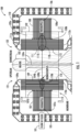
- FIG. 1 a schematic diagram depicting an example layout for an example thermopile-based flow sensing apparatus 100 in accordance with various embodiments of the present disclosure is provided.
- the example thermopile-based flow sensing apparatus 100 may be provided for sensing a flow of fluid 101 (e.g., a flow of a gas or liquid).
- the example thermopile-based flow sensing apparatus 100 may comprise a membrane structure 102.
- the membrane structure 102 may define a heated area 102a on a bulk silicon die 150.
- the example thermopile-based flow sensing apparatus 100 may further comprise a heating structure 103 having a centerline 104a and an axis 104b arranged perpendicular or substantially perpendicular to the centerline 104a.
- the membrane structure 102 may be a thermally isolated structure and may define a heated area 102a.
- the heating structure 103 may be disposed over or otherwise about the membrane structure 102 and is configured to heat the heated area 102a of the membrane structure 102.
- the example thermopile-based flow sensing apparatus 100 may further comprise a first thermopile 105 disposed upstream of the centerline 104a and a second thermopile 106 disposed downstream of the centerline 104a.
- upstream of the centerline 104a is a side of the centerline 104a opposite to a flow direction of the flow of fluid 101.
- downstream of the centerline 104a is a side of the centerline 104a in the flow direction of the flow of fluid 101.
- thermopile 105 may be disposed over or otherwise about the membrane structure 102. In some embodiments, at least a portion of the second thermopile 106 may be disposed over or otherwise about the membrane structure 102.
- the first thermopile 105 may comprise a plurality of first thermocouples 107 disposed upstream of the centerline 104a of the heating structure 103.
- the plurality of first thermocouples 107 are aligned substantially perpendicular to the centerline 104a of the heating structure 103, such that the plurality of first thermocouples 107 have a plurality of first thermocouple junctions 107a (e.g., eleven thermocouple junctions) and a plurality of second thermocouple junctions 107b (e.g., twelve thermocouple junctions).
- the plurality of first thermocouple junctions 107a are disposed out of the heated area 102a and the plurality of second thermocouple junctions 107b are disposed on or substantially adjacent the heated area 102a.
- the second thermopile 106 may comprise a plurality of second thermocouples 108 disposed downstream of the centerline 104a of the heating structure 103.
- the plurality of second thermocouples 108 are aligned substantially perpendicular to the centerline 104a of the heating structure 103, such that the plurality of second thermocouples 108 have a plurality of third thermocouple junctions 108a (e.g., eleven thermocouple junctions) and a plurality of fourth thermocouple junctions 108b (e.g., twelve thermocouple junctions).
- the plurality of third thermocouple junctions 108a are disposed out of the heated area 102a and the plurality of fourth thermocouple junctions 108b are disposed on or substantially adjacent the heated area 102a.
- the first thermopile 105 may further comprise a plurality of third thermocouples 109 disposed on a first side of the axis 104b and upstream of the centerline 104a of the heating structure 103, and a plurality of fourth thermocouples 110 disposed on a second side of the axis 104b and upstream of the centerline 104a of the heating structure 103.
- the plurality of third thermocouples 109 are aligned substantially parallel to the centerline 104a of the heating structure 103, such that the plurality of third thermocouples 109 have a plurality of fifth thermocouple junctions 109a (e.g., six thermocouple junctions) and a plurality of sixth thermocouple junctions 109b (e.g., seven thermocouple junctions).
- a plurality of fifth thermocouple junctions 109a e.g., six thermocouple junctions
- a plurality of sixth thermocouple junctions 109b e.g., seven thermocouple junctions
- the plurality of fourth thermocouples 110 are aligned substantially parallel to the centerline 104a of the heating structure 103, such that the plurality of fourth thermocouples 110 have a plurality of seventh thermocouple junctions 110a (e.g., six thermocouple junctions) and a plurality of eighth thermocouple junctions 110b (e.g., seven thermocouple junctions).
- the plurality of fifth thermocouple junctions 109a are disposed out of the heated area 102a and the plurality of sixth thermocouple junctions 109b are disposed on the heated area 102a.
- the plurality of seventh thermocouple junctions 110a are disposed out of the heated area 102a and the plurality of eighth thermocouple junctions 110b are disposed on the heated area 102a.
- the second thermopile 106 may further comprise a plurality of fifth thermocouples 111 disposed on a first side of the axis 104b and upstream of the centerline 104a of the heating structure 103, and a plurality of sixth thermocouples 112 disposed on a second side of the axis 104b and downstream of the centerline 104a of the heating structure 103.
- the plurality of fifth thermocouples 111 are aligned substantially parallel to the centerline 104a of the heating structure 103, such that the plurality of fifth thermocouples 111 have a plurality of ninth thermocouple junctions 111a (e.g., six thermocouple junctions) and a plurality of tenth thermocouple junctions 111b (e.g., seven thermocouple junctions).
- a plurality of ninth thermocouple junctions 111a e.g., six thermocouple junctions
- a plurality of tenth thermocouple junctions 111b e.g., seven thermocouple junctions
- the plurality of sixth thermocouples 112 are aligned substantially parallel to the centerline 104a of the heating structure 103, such that the plurality of fifth thermocouples 112 have a plurality of eleventh thermocouple junctions 112a (e.g., six thermocouple junctions) and a plurality of twelfth thermocouple junctions 112b (e.g., seven thermocouple junctions).
- eleventh thermocouple junctions 112a e.g., six thermocouple junctions
- twelfth thermocouple junctions 112b e.g., seven thermocouple junctions
- the plurality of ninth thermocouple junctions 111a are disposed out of the heated area 102a and the plurality of tenth thermocouple junctions 111b are disposed on the heated area 102a. In some embodiments, the plurality of eleventh thermocouple junctions 112a are disposed out of the heated area 102a and the plurality of twelfth thermocouple junctions 112b are disposed on the heated area 102a.
- the heating structure 103 may be located between at least two sets of thermocouples (e.g., two thermopiles 105 and 106), with one set of thermocouples located upstream of the heating structure and the other set of thermocouples located downstream of the heating structure.
- each set of thermocouples has one side on the bulk silicon die 150, which can float in temperature.
- T 1 may be measured on the membrane structure 102 using the fourth thermocouple junctions 108b, and T ref (e.g. an ambient temperature of the bulk silicon die 150 positioned out of the heated area 102a) may be measured on the bulk silicon die 150 using the third thermocouple junctions 108a.
- T ref e.g. an ambient temperature of the bulk silicon die 150 positioned out of the heated area 102a
- T ref e.g. an ambient temperature of the bulk silicon die 150 positioned out of the heated area 102a
- T ref e.g. an ambient temperature of the bulk silicon die 150 positioned out of the heated area 102a
- T ref e.g. an ambient temperature of the bulk silicon die 150 positioned out of the heated area 102a
- the bulk silicon die 150 positioned out of the heated area 102a of the membrane structure 102 and the bulk silicon die 150 positioned on the heated area 102a of the membrane structure 102 may have different temperatures due to the heating of the heating structure 103.
- the first thermopile 105 may output a first potential difference that depends on the temperature difference between the bulk silicon die 150 off the membrane structure 102 and on the heated area 102a of the membrane structure 102 in the upstream region 121.
- the second thermopile 106 may output a second potential difference that depends on the temperature difference between the bulk silicon die 150 off the membrane structure 102 and on the heated area 102a of the membrane structure 102 in the downstream region 122.
- the difference between the first potential difference and the second potential difference depends directly, in some examples, on the flow of the fluid 101.
- a flow rate of the flow of the fluid 101 may be measured by calculating the difference between the first potential difference and the second potential difference.
- the number of thermocouple junctions in the thermopile of an example thermopile-based flow sensing apparatus disclosed herein may depend on (e.g., may be a function of) the Seebeck coefficients of the thermocouple materials in the thermocouples of the thermopile and the desired output voltage.
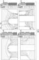
- FIG. 2 a schematic diagram depicting a simulation of temperature distributions and temperature difference distributions on the membrane structure in accordance with various embodiments of the present disclosure is provided.
- example temperature isolines 220 e.g., including, but not limited to, temperature isoline 220A, temperature isoline 220B, and temperature isoline 220C
- example temperature difference isolines 223 disposed around the temperature location 222 and temperature difference isolines 225 disposed around the temperature location 224 are illustrated.
- the temperature distributions and temperature difference distributions on the membrane structure 102 may change with changes in the membrane structure 102 (e.g., shape, thickness), heating structure 103 (e.g., shape, thickness, material(s)), voltage applied to the heating structure 103, and other structures.
- the temperature distributions and temperature difference distributions on the membrane structure 102 may be used to calculate the flow rate of the flow of the fluid 101.
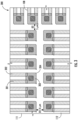
- FIG. 3 a schematic diagram depicting a close-up view 300 of an example thermopile of an example thermopile-based flow sensing apparatus 100 in accordance with various embodiments of the present disclosure is provided.
- an example thermopile 106 (e.g., including, but not limited to, the first thermopile 105 and the second thermopile 106), for an example, may be disposed downstream of the centerline 104a of the heating structure 103.
- the example thermopile 106 may comprise a plurality of second thermocouples 108 aligned substantially perpendicular to the centerline 104a of the heating structure 103, a plurality of fifth thermocouples 111 aligned substantially parallel to the centerline 104a of the heating structure 103, and a plurality of sixth thermocouples 112 aligned substantially parallel to the centerline 104a of the heating structure 103.
- a thermocouple e.g. each of the thermocouples 108, 111, and 112 may comprise a first thermocouple material 301, a second thermocouple material 302, and a thermocouple junction 303, where the first thermocouple material 301 and a second thermocouple material 302 are in contact with each other.
- the thermocouple junction 303 may be shaped as a rectangle. As shown in FIG. 3 , at least one of the corners 304 of the rectangle may be rounded. In some embodiments, the thermocouple junction 303 may be shaped in other forms, such as, including but not limited to, a square. For example, the thermocouple junction 303 may be shaped in a square with at least one rounded corners or at least one rounded edges. For example, the thermocouple junction 303 may be shaped in a circle.
- thermocouple junction 303 may be shaped as a rectangle or a square with all corners rounded.
- thermocouple junction 303 may comprise an interface between the first thermocouple material 301 and the second thermocouple material 302.
- the first thermocouple material may comprise polysilicon
- the second thermocouple material may comprise aluminum.
- the first thermocouple material and the second thermocouple material may comprise differently doped polysilicon (e.g., n-type and p-type polysilicon).
- the first thermocouple material may comprise n-type polysilicon (nPoly Si)
- the second thermocouple material may comprise p-type polysilicon (pPoly Si).
- the first thermocouple material may comprise p-type polysilicon (pPoly Si)
- the second thermocouple material may comprise n-type polysilicon (nPoly Si).
- the first thermocouple material may comprise a nickel-iron alloy (e.g., 60:40 NiFe, 80:20 NiFe), and the second thermocouple material may comprise chromium (Cr), where the difference between the Seebeck coefficients of the thermocouple materials (dS) is about 65 uV/C for 60:40 NiFe and Cr or about 53 uV/C for 80:20 NiFe and Cr.
- a nickel-iron alloy e.g. 60:40 NiFe, 80:20 NiFe
- Cr chromium
- the first thermocouple material may comprise a nickel-iron alloy (e.g., 60:40 NiFe, 80:20 NiFe), and the second thermocouple material may comprise chromium disilicide (CrSi2), where dS is about 105 uV/C for 60:40 NiFe and CrSi2 or about 93 uV/C for 80:20 NiFe and CrSi2.
- the first thermocouple material may comprise a nickel-iron alloy (e.g., 60:40 NiFe, 80:20 NiFe), and the second thermocouple material may comprise rhenium disilicide (ReSi2).
- the first thermocouple material may comprise chromium nitride (e.g., CrN), and the second thermocouple material may comprise copper (Cu), where dS is about 146 uV/C for CrN and Cu.
- the first thermocouple material may comprise chromium nitride (e.g., CrN), and the second thermocouple material may comprise aluminum (Al), where dS is about 138 uV/C for CrN and Al.
- the first thermocouple material may comprise a chromium nitride (e.g., CrN), and the second thermocouple material may comprise p-type polysilicon (pPoly Si), where dS is about 270 uV/C for CrN and pPoly Si.
- CrN chromium nitride
- pPoly Si p-type polysilicon
- the plurality of fifth thermocouples 111 and the plurality of sixth thermocouples 112 are spaced from each other, such that an electrostatic discharge between the plurality of fifth thermocouples 111 and the plurality of sixth thermocouples 112 is reduced.
- a distance D1 between the plurality of fifth thermocouples 111 and the plurality of sixth thermocouples 112 may be in a range from 1 micrometers to 10 micrometers, preferably in a range from 4 micrometers to 8 micrometers, and more preferably at 6 micrometers.
- the plurality of third thermocouples 109 and the plurality of fourth thermocouples 110 are spaced from each other, such that an electrostatic discharge between the plurality of third thermocouples 109 and the plurality of fourth thermocouples 110 is reduced.
- a distance between the plurality of fifth thermocouples 111 and the plurality of sixth thermocouples 112 may be in a range from 1 micrometers to 10 micrometers, preferably in a range from 4 micrometers to 8 micrometers, and more preferably at 6 micrometers.
- the plurality of fifth thermocouples 111 (or the plurality of fifth thermocouples 112) and the plurality of second thermocouples 108 are spaced from each other, such that an electrostatic discharge between the plurality of fifth thermocouples 111 (or the plurality of fifth thermocouples 112) and the plurality of second thermocouples 108 is reduced.
- a distance D2 between the plurality of fifth thermocouples 111 (or the plurality of fifth thermocouples 112) and the plurality of second thermocouples 108 may be in a range from 1 micrometers to 10 micrometers, preferably in a range from 3 micrometers to 7 micrometers, and more preferably at 5 micrometers.
- the plurality of third thermocouples 109 (or the plurality of fourth thermocouples 110) and the plurality of first thermocouples 107 are spaced from each other, such that an electrostatic discharge between the plurality of third thermocouples 109 (or the plurality of fourth thermocouples 110) and the plurality of first thermocouples 107 is reduced.
- a distance between the plurality of third thermocouples 109 (or the plurality of fourth thermocouples 110) and the plurality of first thermocouples 107 may be in a range from 1 micrometers to 10 micrometers, preferably in a range from 3 micrometers to 7 micrometers, and more preferably at 5 micrometers.
- the example thermopile-based flow sensing apparatus 400 may comprise a membrane structure 102 defining a heated area 102a and a heating structure 103 disposed over or otherwise about the membrane structure 102.
- the heating structure 103 may comprise a ribbon, a plate, a wire strip, and/or a layer that may be connected to an electrical power source.
- an electric current may flow through the ribbon, the plate, the wire strip, and/or the layer, which may in turn convert electrical energy to heat energy.
- the electric current may flow through a first portion 103a, the second portion 103b, and the third portion 103c of the heating structure 103.
- the heating structure 103 may impart the heat energy, increase its temperature, and/or elevate the temperature of the heated area 102a of the membrane structure 102.
- the heating structure 103 may comprise a heater with curved, rounded, and non-sharp corners, such that the current density and the heat produced in the corners may be reduced and any breakdown on the heating structure 103 may be prevented.
- the heating structure 103 may have a curved corner 401 at a joint between the first portion 103a and the second portion 103b of the heating structure 103.
- the heating structure 103 may have a curved corner 404 at a joint between the third portion 103c and the second portion 103b of the heating structure 103.
- the heating structure 103 may have a curved corner 403 at a joint between the first portion 103a and a first external connection to the electrical power source.
- a radius of the curved corners 401, 403, 404, or 405 may be in a range from 10 micrometers to 100 micrometers, preferably in a range from 15 micrometers to 50 micrometers, and more preferably in a range from 20 micrometers to 40 micrometers.
- a radius of the curved edge 402 may be in a range from 10 micrometers to 100 micrometers, preferably in a range from 15 micrometers to 50 micrometers, and more preferably in a range from 20 micrometers to 40 micrometers.
- FIG. 5 a schematic diagram depicting a simulation of ohmic loss on a heating structure with sharp corners and curved corners in accordance with various embodiments of the present disclosure is provided.
- the heating structure have sharp corners and the highest power and current density on the heating structure at position A and position C.
- the ohmic losses at position A and position C are approximately 2*10 6 W/cm 3 .
- the heating structure have curved corners 401, 402 and 403.
- the ohmic loss at curved corners 401 and 403 are approximately 1*10 6 W/cm 3 , which are much smaller than the ohmic loss on the heating structure with sharp corners.
- FIG. 6 schematic diagrams depicting example curves of peaking power/current density vs the Fillet radium in accordance with various embodiments of the present disclosure is provided.
- the peaking power density and the peak current density are minimized, in this example, when the Fillet radius of the curved corners 401, 402, and 403 are in a range from 20 micrometers to 40 micrometers.
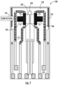
- the example thermopile-based flow sensing apparatus 700 may be provided for sensing a flow of fluid 101 (e.g., a flow of a gas or liquid).
- the example thermopile-based flow sensing apparatus 700 may comprise a membrane structure 102 on a bulk silicon die 150, and a heating structure 103 disposed over or otherwise about the membrane structure 102 and configured to heat a heat area of the membrane structure.
- the example thermopile-based flow sensing apparatus 700 may further comprise a first thermopile 105 disposed upstream of the centerline 104a and a second thermopile 106 disposed downstream of the centerline 104a.
- the example thermopile-based flow sensing apparatus 700 may further comprise at least one resistor 701 disposed around the membrane structure 102.
- the at least one resistor 701 may be configured to control and/or measure a temperature of the bulk silicon die 150 off the membrane structure 102.
- the at least one resistor 701 may be thin-film resistors.
- a cross-section area of the thin-film resistor may have a width in a range from 0.1 micrometers to 50 micrometers, preferably in a range from 1 micrometers to 10 micrometers, and more preferably around 6 micrometers.
- a cross-section area of the heater 103 may have a width in a range from 1 micrometers to 50 micrometers, preferably in a range from 10 micrometers to 20 micrometers, and more preferably around 15 micrometers.
- thermopile-based flow sensing apparatus 800 in accordance with various embodiments of the present disclosure is provided.
- the example thermopile-based flow sensing apparatus 800 may be provided for sensing a flow of fluid 101 (e.g., a flow of a gas or liquid).
- the example thermopile-based flow sensing apparatus 800 may comprise a membrane structure 102 on a bulk silicon die 150, and a heating structure 103 disposed over or otherwise about the membrane structure 102 and configured to heat a heat area of the membrane structure.
- the example thermopile-based flow sensing apparatus 800 may further comprise a first thermopile 105 disposed upstream of the centerline 104a and a second thermopile 106 disposed downstream of the centerline 104a.
- the example thermopile-based flow sensing apparatus 800 may further comprise at least one resistor 701 disposed around the membrane structure 102.
- the at least one resistor 701 may be configured to control and/or measure a temperature of the bulk silicon die 150 off the membrane structure 102.
- the example thermopile-based flow sensing apparatus 800 may further comprise a first electrostatic discharge (ESD) protection circuit 801.
- ESD electrostatic discharge
- the first ESD protection circuit 801 may be placed between the heating structure 103 and an electrical power source for the heating structure 103.
- the first ESD protection circuit 801 is electrically connected with the heating structure in parallel, such that the heating structure 103 of the example thermopile-based flow sensing apparatus 800 may be protected from ESD.
- the first ESD protection circuit 801 may comprise at least one ESD diode.
- the at least one ESD diode may break down and create a low impedance pathway which limits peak voltage/current to the heating structure 103 of the example thermopile-based flow sensing apparatus 800 by diverting the current flow to ground.
- thermopile-based flow sensing apparatus 900 in accordance with various embodiments of the present disclosure is provided.
- the example thermopile-based flow sensing apparatus 900 may be provided for sensing a flow of fluid 101 (e.g., a flow of a gas or liquid).
- the example thermopile-based flow sensing apparatus 900 may comprise a membrane structure 102 on a bulk silicon die 150, and a heating structure 103 disposed over or otherwise about the membrane structure 102 and configured to heat a heat area of the membrane structure.
- the example thermopile-based flow sensing apparatus 900 may further comprise a first thermopile 105 disposed upstream of the centerline 104a and a second thermopile 106 disposed downstream of the centerline 104a.
- the example thermopile-based flow sensing apparatus 900 may further comprise at least one resistor 701 disposed around the membrane structure 102.
- the at least one resistor 701 may be configured to control and/or measure a temperature of the bulk silicon die 150 off the membrane structure 102.
- the example thermopile-based flow sensing apparatus 900 may further comprise a first ESD protection circuit 801.
- the first ESD protection circuit 801 may be placed between the heating structure 103 and an electrical power source for the heating structure 103.
- the first ESD protection circuit 801 is electrically connected with the heating structure in parallel, such that the heating structure 103 of the example thermopile-based flow sensing apparatus 900 may be protected from ESD.
- the example thermopile-based flow sensing apparatus 900 may further comprise a second ESD protection circuit 901.
- the second ESD protection circuit 901 may be placed between the first thermopile 105 and an electrical power source for the first thermopile 105.
- the second ESD protection circuit 901 is electrically connected with the first thermopile 105 in parallel, such that the first thermopile 105 of the example thermopile-based flow sensing apparatus 900 may be protected from ESD.
- the example thermopile-based flow sensing apparatus 900 may further comprise a third ESD protection circuit 902.
- the third ESD protection circuit 902 may be placed between the second thermopile 106 and an electrical power source for the second thermopile 106.
- the third ESD protection circuit 902 is electrically connected with the second thermopile 106 in parallel, such that the second thermopile 106 of the example thermopile-based flow sensing apparatus 900 may be protected from ESD.
- the first ESD protection circuit 801 may comprise at least one ESD diode.
- the at least one ESD diode may break down and create a low impedance pathway which limits peak voltage/current to the heating structure 103 of the example thermopile-based flow sensing apparatus 900 by diverting the current flow to ground.
- the second ESD protection circuit 901 may comprise at least one ESD diode.
- the at least one ESD diode may break down and create a low impedance pathway which limits peak voltage/current to the first thermopile 105 of the example thermopile-based flow sensing apparatus 900 by diverting the current flow to ground.
- the third ESD protection circuit 902 may comprise at least one ESD diode.
- the at least one ESD diode may break down and create a low impedance pathway which limits peak voltage/current to the second thermopile 106 of the example thermopile-based flow sensing apparatus 900 by diverting the current flow to ground.
- thermopile-based flow sensing apparatus 1000 in accordance with various embodiments of the present disclosure is provided.
- the example thermopile-based flow sensing apparatus 1000 may be provided for sensing a flow of fluid 101 (e.g., a flow of a gas or liquid).
- the example thermopile-based flow sensing apparatus 1000 may comprise a membrane structure 102 on a bulk silicon die 150, and a heating structure 103 disposed over or otherwise about the membrane structure 102 and configured to heat a heat area of the membrane structure.
- the example thermopile-based flow sensing apparatus 1000 may further comprise a first thermopile 105 disposed upstream of the centerline 104a and a second thermopile 106 disposed downstream of the centerline 104a.
- the example thermopile-based flow sensing apparatus 1000 may further comprise a first ESD protection circuit 801.
- the first ESD protection circuit 801 may be placed between the heating structure 103 and an electrical power source for the heating structure 103.
- the first ESD protection circuit 801 is electrically connected with the heating structure in parallel, such that the heating structure 103 of the example thermopile-based flow sensing apparatus 1000 may be protected from ESD.
- the first ESD protection circuit 801 may comprise at least one ESD diode.
- the at least one ESD diode may break down and create a low impedance pathway which limits peak voltage/current to the heating structure 103 of the example thermopile-based flow sensing apparatus 1000 by diverting the current flow to ground.
- the example thermopile-based flow sensing apparatus 1000 may further comprise a fourth ESD protection circuit 1001.
- the fourth ESD protection circuit 1001 may be configured to control and/or measure a temperature of the bulk silicon die 150 off the membrane structure 102.
- the fourth ESD protection circuit 1001 may comprise at least one ESD diode.
- FIG. 11 a schematic diagram depicting cross-sectional views for an example ESD diode in accordance with various embodiments of the present disclosure is provided.
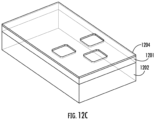
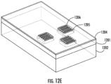
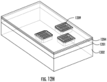
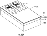
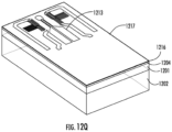
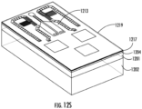
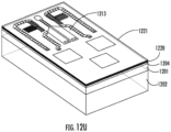
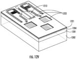
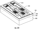
- FIGS. 12A , 12B , 12C , 12D , 12E , 12F , 12G , 12H , 12I , 12J , 12K , 12L , 12M , 12N , 12O , 12P , 12Q , 12R , 12S , 12T , 12U , 12V , 12W , 12X , 12Y , 12Z , 12AA , and 12BB schematic diagrams depicting an example process flow for fabricating an example thermopile-based flow sensing apparatus in accordance with some example embodiments are provided.
- the example process flow may begin with fabricating an N-type epitaxial layer 1201 on a top surface of a substrate 1202 (e.g., a silicon die or wafer).
- a substrate 1202 e.g., a silicon die or wafer.
- the example process flow may comprise fabricating (e.g., by thermal oxidation) a thermal oxidation layer 1203 on a top surface of the N-type epitaxial layer 1201.
- the example process flow may comprise fabricating (e.g., by etching with a mask) a P-well masked layer 1204 by removing a portion of the thermal oxidation layer 1203.
- the example process flow may comprise fabricating (e.g., by implantation/diffusion) a P-well implantation/diffusion layer 1205.
- the example process flow may comprise fabricating (e.g., by etching with a mask) an N-plus masked oxidation layer 1206.
- the example process flow may comprise fabricating (e.g., by diffusion) an N-plus POCL3 diffusion layer 1207.
- the example process flow may comprise fabricating (e.g., by deposition) a low pressure chemical vapor deposition (LPCVD) nitride layer 1208 on the p-well masked layer 1204.
- LPCVD low pressure chemical vapor deposition
- the example process flow may comprise fabricating (e.g., by etching with a mask) the P-plus masked nitride layer 1209 by removing a portion of the LPCVD nitride layer 1208.
- the example process flow may comprise fabricating (e.g., by diffusion) a P-plus BBR3 diffusion layer 1210.
- the example process flow may comprise striping the LPCVD nitride layer 1208.
- the example process flow may comprise sputtering deposition of a low stress nitride layer 1211.
- the example process flow may comprise fabricating (e.g., by deposition) a metal film deposition layer 1212 for the heating structure on the low stress nitride layer 1211.
- the example process flow may comprise fabricating (e.g., by etching with a mask) a masked definition layer 1213 for the heating structure.
- the example process flow may comprise sputtering a low stress nitride layer 1214 on a top surface of the masked definition layer 1213.
- the example process flow may comprise fabricating (e.g., by deposition) a first thermopile material layer 1215 on a top surface of the low stress nitride layer 1214.
- the example process flow may comprise fabricating (e.g., by etching with a mask) a masked first thermopile material layer 1216.
- the example process flow may comprise sputtering a low stress nitride layer 1217 on a top surface of the masked first thermopile material layer 1216.
- the example process flow may comprise etching masked vias 1218.
- the example process flow may comprise fabricating (e.g., by deposition) a second thermopile material layer 1219 on a top surface of the low stress nitride layer 1217.
- the example process flow may comprise fabricating (e.g., by etching with a mask) a masked second thermopile material layer 1220.
- the example process flow may comprise sputtering a low stress nitride layer 1221 on a top surface of the masked second thermopile material layer 1220.
- the example process flow may comprise etching the low stress nitride layer 1221 for contacts 1222.
- the example process flow may comprise etching the N-plus masked oxidation layer 1206 for contacts 1222.
- the example process flow may comprise depositing a metal layer 1223 on a top surface of the low stress nitride layer 1221.
- the example process flow may comprise fabricating (e.g., by etching with a mask) a masked metal layer 1224.
- the example process flow may comprise fabricating (e.g., by deposition) a plasma-enhanced chemical vapor deposition (PECVD) passivation nitride layer 1225 on the masked metal layer 1224.
- PECVD plasma-enhanced chemical vapor deposition
- the example process flow may comprise etching the PECVD passivation nitride layer 1225 to expose bond pads 1226.
- the example process flow may comprise etching the backside diaphragm 1226 of the substrate 1202 to form the example thermopile-based flow sensing apparatus.
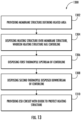
- FIG. 13 an example flowchart diagram illustrating an example method 1300 for manufacturing or otherwise providing an apparatus (e.g., apparatus 100, 400, 700, 800, 900, and 1000) for sensing a flow of fluid according to some example embodiments described herein is provided.
- apparatus e.g., apparatus 100, 400, 700, 800, 900, and 1000
- a membrane structure defining a heated area is provided.
- a membrane structure 102 is provided to define a heated area 102a on a bulk silicon die 150.
- a heating structure is disposed over or otherwise about the membrane structure.
- a heating structure 103 with a centerline 104a is disposed over or otherwise about the membrane structure 102.
- the heating structure 103 may comprise a heater with curved, rounded, and/or non-sharp corners, such that the current density and the heat produced in the corners may be reduced and any breakdown on the heating structure 103 may be prevented.
- the heating structure 103 may have a curved corner 401 at a j oint between the first portion 103a and 103b of the heating structure 103.
- the heating structure 103 may have a curved corner at a joint between the third portion 103ac and 103b of the heating structure 103.
- the heating structure 103 may have a curved corner 403 at a joint between the first portion 103a and a first external connection to the electrical power source. Similarly, in some examples, the heating structure 103 may have a curved corner at a joint between the third portion 103c and a second external connection to the electrical power source. In additional examples, the heating structure 103 may have a curved edge 402 connecting the first portion 103a and the third portion 103c.
- a first thermopile is disposed upstream of the centerline.
- a first thermopile 105 is disposed upstream of the centerline 104a.
- the first thermopile 105 may comprise a plurality of first thermocouples 107 and at least a portion of the plurality of first thermocouples 107 are disposed over or otherwise about the membrane structure 102. In some embodiments, each junction of the plurality of first thermocouples 107 has rounded corners.
- a second thermopile is disposed downstream of the centerline.
- a second thermopile 106 is disposed downstream of the centerline 104a.
- the second thermopile 106 may comprise a plurality of second thermocouples 108 and at least a portion of the plurality of second thermocouples 108 are disposed over or otherwise about the membrane structure 102. In some embodiments, each junction of the plurality of second thermocouples 108 has rounded corners.
- the first ESD protection circuit 801 may be placed between the heating structure 103 and an electrical power source for the heating structure 103. In some examples, the first ESD protection circuit 801 is electrically connected with the heating structure 103 in parallel, such that the heating structure 103 of the example thermopile-based flow sensing apparatus 800 may be protected from ESD.
- the first ESD protection circuit 801 may comprise at least one ESD diode.
- the at least one ESD diode may break down and create a low impedance pathway which limits peak voltage/current to the electric components of the example thermopile-based flow sensing apparatus 800 by diverting the current flow to ground.
- operations 1302, 1304, 1306, 1308, and 1310 may not necessarily occur in the order depicted in FIG. 13 .
- one or more of the operations depicted in FIG. 13 may occur substantially simultaneously.
- one or more additional operations may be involved before, after, or between any of the operations shown in FIG. 13 .
- FIG. 13 thus illustrate an example flowchart describing operations performed in accordance with example embodiments of the present disclosure. It will be understood that each operation of the flowcharts, and combinations of operations in the flowcharts, may be implemented by various means, such as devices comprising hardware, firmware, one or more processors, and/or circuitry associated with execution of software comprising one or more computer program instructions.
- one or more of the procedures described above may be performed by execution of program code instructions.
- material handling equipment e.g., a robotic arm, servo motor, motion controllers, and the like
- computer program instructions residing on a non-transitory computer-readable storage memory.
- the program code instructions that, when executed, cause performance of the procedures described above may be stored by a non-transitory computer-readable storage medium (e.g., memory) of a computing apparatus and executed by a processor of the computing apparatus.
- the computer program instructions which embody the procedures described above may be stored by a memory of an apparatus employing an embodiment of the present disclosure and executed by a processor of the apparatus.
- any such computer program instructions may be loaded onto a computer or other programmable apparatus (e.g., hardware) to produce a machine, such that the resulting computer or other programmable apparatus provides for implementation of the functions specified in the method 1300.
- the instructions stored in the computer-readable storage memory produce an article of manufacture configured to implement the various functions specified in the method 1300.
- the program code instructions may also be loaded onto a computer or other programmable apparatus to cause a series of operations to be performed on the computer or other programmable apparatus to produce a computer-implemented process such that the instructions executed on the computer or other programmable apparatus provide operations for implementing the functions specified in the operations of method 1300.
- execution of a computer or other processing circuitry to perform various functions converts the computer or other processing circuitry into a particular machine configured to perform an example embodiment of the present disclosure.
- the flowchart operations described with reference to FIG. 13 support combinations of means for performing the specified functions and combinations of operations for performing the specified functions. It will be understood that one or more operations of the flowcharts, and combinations of operations in the flowcharts, may be implemented by special purpose hardware-based computer systems which perform the specified functions, or combinations of special purpose hardware and computer instructions.
- certain ones of the operations herein may be modified or further amplified as described below. Moreover, in some embodiments additional optional operations may also be included. It should be appreciated that each of the modifications, optional additions or amplifications described herein may be included with the operations herein either alone or in combination with any others among the features described herein.
Landscapes
- Physics & Mathematics (AREA)
- Fluid Mechanics (AREA)
- General Physics & Mathematics (AREA)
- Measuring Volume Flow (AREA)
Abstract
Description
- Exemplary embodiments of the present disclosure relate generally to flow sensing apparatuses, and more particularly, to thermopile-based flow sensing apparatuses.
- Thermopile-based flow sensors may be used to measure a flow rate and/or quantity of a flowing media (e.g., moving liquid or gaseous substance) and may be implemented in various applications. Such flow sensing apparatuses are plagued by technical challenges and limitations. Through applied effort, ingenuity, and innovation, many of these identified problems have been solved by developing solutions that are included in embodiments of the present disclosure, many examples of which are described in detail herein.
- Various embodiments described herein relate to methods, apparatuses, and systems for improving sensitivity and performance of an apparatus such as, for example, a flow sensing apparatus.
- In accordance with various examples of the present disclosure, an apparatus for sensing a flow of fluid is provided. The apparatus includes, but not limited to: a membrane structure defining a heated area; a heating structure disposed over the membrane structure and configured to heat the heated area, where the heating structure has a centerline; a first thermopile including a plurality of first thermocouples disposed upstream of the centerline, where at least a portion of the plurality of first thermocouples are disposed over the membrane structure and each junction of the plurality of first thermocouples has rounded corners; and a second thermopile including a plurality of second thermocouples disposed downstream of the centerline, where at least a portion of the plurality of second thermocouples are disposed over the membrane structure and each junction of the plurality of second thermocouples has rounded corners.
- In some embodiments, the heating structure comprises a heater with curved and non-sharp corners.
- In some embodiments, the apparatus further includes, but not limited to an electrostatic discharge (ESD) circuit with a diode to protect the heating structure during an ESD pulse, wherein the ESD circuit is electrically connected with the heating structure in parallel.
- In some embodiments, the diode is an ESD diode that breaks down and creates a pathway to divert a current away from the heating structure.
- In some embodiments, the apparatus further includes, but not limited to an electrostatic discharge (ESD) circuit with a diode to protect the first thermopile during an ESD pulse.
- In some embodiments, the diode is an ESD diode that breaks down and creates a pathway to divert a current away from the first thermopile.
- In some embodiments, the apparatus further includes, but not limited to an electrostatic discharge (ESD) circuit with a diode to protect the second thermopile during an ESD pulse.
- In some embodiments, the diode is an ESD diode that breaks down and creates a pathway to divert a current away from the second thermopile.
- In some embodiments, the apparatus further includes, but not limited to at least one thin-film resistor configured to measure an ambient temperature out of the heated area.
- In some embodiments, the apparatus further includes, but not limited to a diode configured to measure an ambient temperature out of the heated area.
- In some embodiments, the plurality of first thermocouples are aligned perpendicular to the centerline, and the plurality of second thermocouples are aligned perpendicular to the centerline.
- In some embodiments, the heating structure has an axis perpendicular to the centerline, wherein: the first thermopile including a plurality of third thermocouples disposed upstream of the centerline and on a first side of the axis and a plurality of fourth thermocouples disposed upstream of the centerline and on a second side of the axis, and the second thermopile including a plurality of fifth thermocouples disposed downstream of the centerline and on the first side of the axis and a plurality of sixth thermocouples disposed downstream of the centerline and on the second side of the axis.
- In some embodiments, each of the plurality of first thermocouples includes, but not limited to a first interface between a first thermocouple material and a second thermocouple material, and each of the plurality of second thermocouples includes, but not limited to a second interface between the first thermocouple material and the second thermocouple material.
- In some embodiments, the first thermocouple material includes, but not limited to n-type polysilicon, and the second thermocouple material includes, but not limited to p-type polysilicon.
- In some embodiments, the first thermocouple material includes, but not limited to a nickel-iron alloy, and wherein the second thermocouple material includes, but not limited to chromium, chromium disilicide, or rhenium disilicide.
- In some embodiments, the first thermocouple material includes, but not limited to chromium nitride, and wherein the second thermocouple material includes, but not limited to copper or aluminum.
- In accordance with various examples of the present disclosure, a method for manufacturing an apparatus for sensing a flow of fluid is provided. The method includes, but not limited to: providing a membrane structure defining a heated area; disposing a heating structure over the membrane structure, wherein the heating structure has a centerline; disposing a first thermopile upstream of the centerline, wherein the first thermopile includes a plurality of first thermocouples, at least a portion of the plurality of first thermocouples are disposed over the membrane structure, and each junction of the plurality of first thermocouples has rounded corners; and disposing a second thermopile disposed downstream of the centerline, wherein the second thermopile includes a plurality of second thermocouples, at least a portion of the plurality of second thermocouples are disposed over the membrane structure, and each junction of the plurality of second thermocouples has rounded corners.
- In some embodiments, the heating structure includes, but not limited to a heater with curved and non-sharp corners.
- In some embodiments, the method further includes, but not limited to providing an electrostatic discharge (ESD) circuit with a diode to protect the heating structure during an ESD pulse.
- In some embodiments, the diode is an ESD diode that breaks down and creates a pathway to divert a current away from the heating structure, wherein the ESD circuit is electrically connected with the heating structure in parallel.
- The description of the illustrative embodiments may be read in conjunction with the accompanying figures. It will be appreciated that, for simplicity and clarity of illustration, elements illustrated in the figures have not necessarily been drawn to scale, unless described otherwise. For example, the dimensions of some of the elements may be exaggerated relative to other elements, unless described otherwise. Embodiments incorporating teachings of the present disclosure are shown and described with respect to the figures presented herein, in which:
-
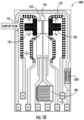
FIG. 1 illustrates a schematic diagram depicting an example layout for an example thermopile-based flow sensing apparatus in accordance with various embodiments of the present disclosure; -
FIG. 2 illustrates a schematic diagram depicting a simulation of temperature distributions and temperature difference distributions on the membrane structure in accordance with various embodiments of the present disclosure; -
FIG. 3 illustrates a schematic diagram depicting a close-up view of a thermopile of an example thermopile-based flow sensing apparatus in accordance with various embodiments of the present disclosure; -
FIG. 4 illustrates a schematic diagram depicting an example layout of an example thermopile-based flow sensing apparatus in accordance with various embodiments of the present disclosure; -
FIG. 5 illustrates a schematic diagram depicting a simulation of the ohmic loss on a heating structure with sharp corners in accordance with various embodiments of the present disclosure; -
FIG. 6 illustrates a schematic diagram depicting example curves of peaking power/current density vs the Fillet radium in accordance with various embodiments of the present disclosure; -
FIG. 7 illustrates a schematic diagram depicting an example layout for an example thermopile-based flow sensing apparatus in accordance with various embodiments of the present disclosure; -
FIG. 8 illustrates a schematic diagram depicting an example layout for an example thermopile-based flow sensing apparatus in accordance with various embodiments of the present disclosure; -
FIG. 9 illustrates a schematic diagram depicting an example layout for an example thermopile-basedflow sensing apparatus 900 in accordance with various embodiments of the present disclosure; -
FIG. 10 illustrates a schematic diagram depicting an example layout for an example thermopile-basedflow sensing apparatus 1000 in accordance with various embodiments of the present disclosure; -
FIG. 11 illustrates a schematic diagram depicting cross-sectional views for an example ESD diode in accordance with various embodiments of the present disclosure; -
FIGS. 12A ,12B ,12C ,12D ,12E ,12F ,12G ,12H ,12I ,12J ,12K ,12L ,12M ,12N ,12O ,12P ,12Q ,12R ,12S ,12T ,12U ,12V ,12W ,12X ,12Y ,12Z ,12AA , and 12BB illustrate an example process flow for fabricating an example thermopile-based flow sensing apparatus in accordance with various embodiments of the present disclosure; and -
FIG. 13 illustrates an example flowchart diagram depicting an example method for manufacturing or otherwise providing an apparatus for sensing a flow of fluid in accordance with various embodiments of the present disclosure. - Some embodiments of the present disclosure will now be described more fully hereinafter with reference to the accompanying drawings, in which some, but not all embodiments of the disclosure are shown. Indeed, these disclosures may be embodied in many different forms and should not be construed as limited to the embodiments set forth herein; rather, these embodiments are provided so that this disclosure will satisfy applicable legal requirements. Like numbers refer to like elements throughout.
- The components illustrated in the figures represent components that may or may not be present in various embodiments of the present disclosure described herein such that embodiments may include fewer or more components than those shown in the figures while not departing from the scope of the present disclosure. Some components may be omitted from one or more figures or shown in a dashed line for visibility of the underlying components.
- The phrases "in an example embodiment," "some embodiments," "various embodiments," and the like generally mean that the particular feature, structure, or characteristic following the phrase may be included in at least one embodiment of the present disclosure, and may be included in more than one embodiment of the present disclosure (importantly, such phrases do not necessarily refer to the same embodiment).
- The word "example" or "exemplary" is used herein to mean "serving as an example, instance, or illustration." Any implementation described herein as "exemplary" is not necessarily to be construed as preferred or advantageous over other implementations.
- If the specification states a component or feature "may," "can," "could," "should," "would," "preferably," "possibly," "typically," "optionally," "for example," "often," or "might" (or other such language) be included or have a characteristic, that a specific component or feature is not required to be included or to have the characteristic. Such components or features may be optionally included in some embodiments, or may be excluded.
- The term "electronically coupled" or "in electronic communication with" in the present disclosure refers to two or more electrical elements (for example, but not limited to, an example processing circuitry, communication module, input/output module memory, humidity sensing component, cooling element, gas detection component) and/or electric circuit(s) being connected through wired means (for example but not limited to, conductive wires or traces) and/or wireless means (for example but not limited to, wireless network, electromagnetic field), such that data and/or information (for example, electronic indications, signals) may be transmitted to and/or received from the electrical elements and/or electric circuit(s) that are electronically coupled.
- The term "flow sensing apparatus" may refer to an apparatus that may detect, measure, and/or identify flow rate(s) (including, but not limited to, linear flow velocity, nonlinear flow velocity, mass flow rate, and/or volumetric flow rate) of a flowing media or medium. In the present disclosure, the term "flowing media" refers to a substance (such as, but not limited to, a liquid substance and/or a gaseous substance, such as air).
- The term "thermopile" may refer to an electrical device comprising a plurality of thermocouples connected in series or parallel to convert thermal energy into electrical energy. In the present disclosure, the term "thermocouple" refers to an electrical device containing two wires made of different metals joined together to produce an electrical current at differing temperatures.
- Thermopile-based flow sensing apparatuses may be utilized in a variety of applications including medical and industrial applications. For example, thermopile-based flow sensing apparatuses may be utilized in drug delivery, respirators, ventilators, anesthesia machines, and/or the like. For example, a thermopile-based flow sensing apparatus may be implemented in a patient requiring treatment such as, but are not limited to, for drug delivery, dialysis or hematology.
- In some examples, precise measurement and/or control for the thermopile-based flow sensing apparatuses may be required. In some examples, the thermopile-based flow sensing apparatuses may include thermopiles and a heating structure. In such examples, electrostatic discharges (ESD) may affect transducer in the thermopile-based flow sensing apparatuses. For example, thermopiles of the thermopile-based flow sensing apparatuses are highly sensitive to the ESD. For example, the heat structure may also be susceptible to the ESD at some locations of the heating structure. For example, a disposable flow sensor or any other flow sensor with external electrical connections that may be touched by someone handling them may need the ESD protection.
- In some additional examples, an ESD may pass current to the patient if the thermopile-based flow sensing apparatuses are damaged due to the ESD. Additionally or alternatively, performance of thermopile-based flow sensing apparatuses may be negatively impacted, in some examples, by an ESD.
- Using the systems, apparatuses and techniques disclosed herein, example thermopile-based flow sensing apparatuses configured to be protected from an ESD thereof are provided. The example thermopile-based flow sensing apparatuses, in some embodiments, may comprise thermopiles with thermocouples having rounded or otherwise dulled (e.g., not sharp or angled) corners. In some embodiments, an example thermopile-based flow sensing apparatus may comprise a heating structure having curved, rounded, and/or non-sharp corners. In some embodiments, an example thermopile-based flow sensing apparatus may further comprise an electrostatic discharge (ESD) protection circuit to protect electric components of the example thermopile-based flow sensing apparatuses from the ESD.
- To address exemplary challenges and limitations associated with measuring flow rates, various examples of the present disclosure may be provided. For example, various examples of the present disclosure may provide example thermopile-based flow sensing apparatuses, methods, computer program products, and systems.
- Referring now to
FIG. 1 , a schematic diagram depicting an example layout for an example thermopile-basedflow sensing apparatus 100 in accordance with various embodiments of the present disclosure is provided. - In some embodiments, the example thermopile-based
flow sensing apparatus 100 may be provided for sensing a flow of fluid 101 (e.g., a flow of a gas or liquid). In some embodiments, the example thermopile-basedflow sensing apparatus 100 may comprise amembrane structure 102. For example, themembrane structure 102 may define aheated area 102a on a bulk silicon die 150. The example thermopile-basedflow sensing apparatus 100 may further comprise aheating structure 103 having acenterline 104a and anaxis 104b arranged perpendicular or substantially perpendicular to thecenterline 104a. In some examples, themembrane structure 102 may be a thermally isolated structure and may define aheated area 102a. In some examples, theheating structure 103 may be disposed over or otherwise about themembrane structure 102 and is configured to heat theheated area 102a of themembrane structure 102. - In some embodiments, the example thermopile-based
flow sensing apparatus 100 may further comprise afirst thermopile 105 disposed upstream of thecenterline 104a and asecond thermopile 106 disposed downstream of thecenterline 104a. For example, upstream of thecenterline 104a is a side of thecenterline 104a opposite to a flow direction of the flow offluid 101. For example, downstream of thecenterline 104a is a side of thecenterline 104a in the flow direction of the flow offluid 101. - In some embodiments, at least a portion of the
first thermopile 105 may be disposed over or otherwise about themembrane structure 102. In some embodiments, at least a portion of thesecond thermopile 106 may be disposed over or otherwise about themembrane structure 102. - In some embodiments, the
first thermopile 105 may comprise a plurality offirst thermocouples 107 disposed upstream of thecenterline 104a of theheating structure 103. In some embodiments, the plurality offirst thermocouples 107 are aligned substantially perpendicular to thecenterline 104a of theheating structure 103, such that the plurality offirst thermocouples 107 have a plurality offirst thermocouple junctions 107a (e.g., eleven thermocouple junctions) and a plurality ofsecond thermocouple junctions 107b (e.g., twelve thermocouple junctions). - In some embodiments, the plurality of
first thermocouple junctions 107a are disposed out of theheated area 102a and the plurality ofsecond thermocouple junctions 107b are disposed on or substantially adjacent theheated area 102a. - In some embodiments, the
second thermopile 106 may comprise a plurality ofsecond thermocouples 108 disposed downstream of thecenterline 104a of theheating structure 103. In some embodiments, the plurality ofsecond thermocouples 108 are aligned substantially perpendicular to thecenterline 104a of theheating structure 103, such that the plurality ofsecond thermocouples 108 have a plurality ofthird thermocouple junctions 108a (e.g., eleven thermocouple junctions) and a plurality offourth thermocouple junctions 108b (e.g., twelve thermocouple junctions). - In some embodiments, the plurality of
third thermocouple junctions 108a are disposed out of theheated area 102a and the plurality offourth thermocouple junctions 108b are disposed on or substantially adjacent theheated area 102a. - In some embodiments, the
first thermopile 105 may further comprise a plurality ofthird thermocouples 109 disposed on a first side of theaxis 104b and upstream of thecenterline 104a of theheating structure 103, and a plurality offourth thermocouples 110 disposed on a second side of theaxis 104b and upstream of thecenterline 104a of theheating structure 103. In some embodiments, the plurality ofthird thermocouples 109 are aligned substantially parallel to thecenterline 104a of theheating structure 103, such that the plurality ofthird thermocouples 109 have a plurality offifth thermocouple junctions 109a (e.g., six thermocouple junctions) and a plurality ofsixth thermocouple junctions 109b (e.g., seven thermocouple junctions). In some embodiments, the plurality offourth thermocouples 110 are aligned substantially parallel to thecenterline 104a of theheating structure 103, such that the plurality offourth thermocouples 110 have a plurality of seventh thermocouple junctions 110a (e.g., six thermocouple junctions) and a plurality ofeighth thermocouple junctions 110b (e.g., seven thermocouple junctions). - In some embodiments, the plurality of
fifth thermocouple junctions 109a are disposed out of theheated area 102a and the plurality ofsixth thermocouple junctions 109b are disposed on theheated area 102a. In some embodiments, the plurality of seventh thermocouple junctions 110a are disposed out of theheated area 102a and the plurality ofeighth thermocouple junctions 110b are disposed on theheated area 102a. - In some embodiments, the
second thermopile 106 may further comprise a plurality offifth thermocouples 111 disposed on a first side of theaxis 104b and upstream of thecenterline 104a of theheating structure 103, and a plurality ofsixth thermocouples 112 disposed on a second side of theaxis 104b and downstream of thecenterline 104a of theheating structure 103. In some embodiments, the plurality offifth thermocouples 111 are aligned substantially parallel to thecenterline 104a of theheating structure 103, such that the plurality offifth thermocouples 111 have a plurality ofninth thermocouple junctions 111a (e.g., six thermocouple junctions) and a plurality of tenth thermocouple junctions 111b (e.g., seven thermocouple junctions). In some embodiments, the plurality ofsixth thermocouples 112 are aligned substantially parallel to thecenterline 104a of theheating structure 103, such that the plurality offifth thermocouples 112 have a plurality ofeleventh thermocouple junctions 112a (e.g., six thermocouple junctions) and a plurality oftwelfth thermocouple junctions 112b (e.g., seven thermocouple junctions). - In some embodiments, the plurality of
ninth thermocouple junctions 111a are disposed out of theheated area 102a and the plurality of tenth thermocouple junctions 111b are disposed on theheated area 102a. In some embodiments, the plurality ofeleventh thermocouple junctions 112a are disposed out of theheated area 102a and the plurality oftwelfth thermocouple junctions 112b are disposed on theheated area 102a. - In some embodiments, as discussed with reference to
FIG. 1 , theheating structure 103 may be located between at least two sets of thermocouples (e.g., twothermopiles 105 and 106), with one set of thermocouples located upstream of the heating structure and the other set of thermocouples located downstream of the heating structure. In these arrangements, each set of thermocouples has one side on the bulk silicon die 150, which can float in temperature. - In some embodiments, the following equation may be used to characterize the thermopile-based flow sensing apparatus disclosed herein:

FIG. 1 , T 1 may be measured on themembrane structure 102 using thefourth thermocouple junctions 108b, and T ref (e.g. an ambient temperature of the bulk silicon die 150 positioned out of theheated area 102a) may be measured on the bulk silicon die 150 using thethird thermocouple junctions 108a. In other instances, such as is shown inFIG. 1 , the relative temperature difference T 1 may be measured on themembrane structure 102 using thesecond thermocouple junctions 107b and T ref may be measured on the bulk silicon die 150 using thefirst thermocouple junctions 107a. - In some embodiments, as shown in
FIG. 1 , the bulk silicon die 150 positioned out of theheated area 102a of themembrane structure 102 and the bulk silicon die 150 positioned on theheated area 102a of themembrane structure 102 may have different temperatures due to the heating of theheating structure 103. For example, thefirst thermopile 105 may output a first potential difference that depends on the temperature difference between the bulk silicon die 150 off themembrane structure 102 and on theheated area 102a of themembrane structure 102 in theupstream region 121. For example, thesecond thermopile 106 may output a second potential difference that depends on the temperature difference between the bulk silicon die 150 off themembrane structure 102 and on theheated area 102a of themembrane structure 102 in thedownstream region 122. - In some embodiments, the difference between the first potential difference and the second potential difference depends directly, in some examples, on the flow of the
fluid 101. In some embodiments, a flow rate of the flow of the fluid 101 may be measured by calculating the difference between the first potential difference and the second potential difference. - In some embodiments, the number of thermocouple junctions in the thermopile of an example thermopile-based flow sensing apparatus disclosed herein may depend on (e.g., may be a function of) the Seebeck coefficients of the thermocouple materials in the thermocouples of the thermopile and the desired output voltage.
- Referring now to
FIG. 2 , a schematic diagram depicting a simulation of temperature distributions and temperature difference distributions on the membrane structure in accordance with various embodiments of the present disclosure is provided. - As shown on the left of
FIG. 2 , locations of hot thermocouples are demonstrated. On the right top ofFIG. 2 , example temperature isolines 220 (e.g., including, but not limited to,temperature isoline 220A,temperature isoline 220B, and temperature isoline 220C) for an example thermopile-based flow sensing apparatus are illustrated. On the right bottom ofFIG. 2 , exampletemperature difference isolines 223 disposed around thetemperature location 222 andtemperature difference isolines 225 disposed around thetemperature location 224 are illustrated. - In some embodiments, the temperature distributions and temperature difference distributions on the
membrane structure 102 may change with changes in the membrane structure 102 (e.g., shape, thickness), heating structure 103 (e.g., shape, thickness, material(s)), voltage applied to theheating structure 103, and other structures. In some embodiments, the temperature distributions and temperature difference distributions on themembrane structure 102 may be used to calculate the flow rate of the flow of thefluid 101. - Referring now to
FIG. 3 , a schematic diagram depicting a close-upview 300 of an example thermopile of an example thermopile-basedflow sensing apparatus 100 in accordance with various embodiments of the present disclosure is provided. - In some embodiments, as shown in
FIG. 3 , an example thermopile 106 (e.g., including, but not limited to, thefirst thermopile 105 and the second thermopile 106), for an example, may be disposed downstream of thecenterline 104a of theheating structure 103. Theexample thermopile 106 may comprise a plurality ofsecond thermocouples 108 aligned substantially perpendicular to thecenterline 104a of theheating structure 103, a plurality offifth thermocouples 111 aligned substantially parallel to thecenterline 104a of theheating structure 103, and a plurality ofsixth thermocouples 112 aligned substantially parallel to thecenterline 104a of theheating structure 103. - In some embodiments, as shown in
FIG. 3 , a thermocouple ( e.g. each of thethermocouples first thermocouple material 301, asecond thermocouple material 302, and athermocouple junction 303, where thefirst thermocouple material 301 and asecond thermocouple material 302 are in contact with each other. - In some embodiments, the
thermocouple junction 303 may be shaped as a rectangle. As shown inFIG. 3 , at least one of thecorners 304 of the rectangle may be rounded. In some embodiments, thethermocouple junction 303 may be shaped in other forms, such as, including but not limited to, a square. For example, thethermocouple junction 303 may be shaped in a square with at least one rounded corners or at least one rounded edges. For example, thethermocouple junction 303 may be shaped in a circle. - In some embodiments, the
thermocouple junction 303 may be shaped as a rectangle or a square with all corners rounded. - In some embodiments, the
thermocouple junction 303 may comprise an interface between thefirst thermocouple material 301 and thesecond thermocouple material 302. - In some embodiments, the first thermocouple material may comprise polysilicon, and the second thermocouple material may comprise aluminum. In some embodiments, the first thermocouple material and the second thermocouple material may comprise differently doped polysilicon (e.g., n-type and p-type polysilicon). For example, the first thermocouple material may comprise n-type polysilicon (nPoly Si), and the second thermocouple material may comprise p-type polysilicon (pPoly Si). In another example, the first thermocouple material may comprise p-type polysilicon (pPoly Si), and the second thermocouple material may comprise n-type polysilicon (nPoly Si).
- In some embodiments, the first thermocouple material may comprise a nickel-iron alloy (e.g., 60:40 NiFe, 80:20 NiFe), and the second thermocouple material may comprise chromium (Cr), where the difference between the Seebeck coefficients of the thermocouple materials (dS) is about 65 uV/C for 60:40 NiFe and Cr or about 53 uV/C for 80:20 NiFe and Cr. In some embodiments, the first thermocouple material may comprise a nickel-iron alloy (e.g., 60:40 NiFe, 80:20 NiFe), and the second thermocouple material may comprise chromium disilicide (CrSi2), where dS is about 105 uV/C for 60:40 NiFe and CrSi2 or about 93 uV/C for 80:20 NiFe and CrSi2. In some embodiments, the first thermocouple material may comprise a nickel-iron alloy (e.g., 60:40 NiFe, 80:20 NiFe), and the second thermocouple material may comprise rhenium disilicide (ReSi2).
- In some embodiments, the first thermocouple material may comprise chromium nitride (e.g., CrN), and the second thermocouple material may comprise copper (Cu), where dS is about 146 uV/C for CrN and Cu. In some embodiments, the first thermocouple material may comprise chromium nitride (e.g., CrN), and the second thermocouple material may comprise aluminum (Al), where dS is about 138 uV/C for CrN and Al. In some embodiments, the first thermocouple material may comprise a chromium nitride (e.g., CrN), and the second thermocouple material may comprise p-type polysilicon (pPoly Si), where dS is about 270 uV/C for CrN and pPoly Si.
- In some embodiments, as shown in
FIG. 3 , the plurality offifth thermocouples 111 and the plurality ofsixth thermocouples 112 are spaced from each other, such that an electrostatic discharge between the plurality offifth thermocouples 111 and the plurality ofsixth thermocouples 112 is reduced. For example, a distance D1 between the plurality offifth thermocouples 111 and the plurality ofsixth thermocouples 112 may be in a range from 1 micrometers to 10 micrometers, preferably in a range from 4 micrometers to 8 micrometers, and more preferably at 6 micrometers. - Similarly, in some embodiments, the plurality of
third thermocouples 109 and the plurality offourth thermocouples 110 are spaced from each other, such that an electrostatic discharge between the plurality ofthird thermocouples 109 and the plurality offourth thermocouples 110 is reduced. For example, a distance between the plurality offifth thermocouples 111 and the plurality ofsixth thermocouples 112 may be in a range from 1 micrometers to 10 micrometers, preferably in a range from 4 micrometers to 8 micrometers, and more preferably at 6 micrometers. - In some embodiments, as shown in
FIG. 3 , the plurality of fifth thermocouples 111 (or the plurality of fifth thermocouples 112) and the plurality ofsecond thermocouples 108 are spaced from each other, such that an electrostatic discharge between the plurality of fifth thermocouples 111 (or the plurality of fifth thermocouples 112) and the plurality ofsecond thermocouples 108 is reduced. For example, a distance D2 between the plurality of fifth thermocouples 111 (or the plurality of fifth thermocouples 112) and the plurality ofsecond thermocouples 108 may be in a range from 1 micrometers to 10 micrometers, preferably in a range from 3 micrometers to 7 micrometers, and more preferably at 5 micrometers. - Similarly, in some embodiments, the plurality of third thermocouples 109 (or the plurality of fourth thermocouples 110) and the plurality of
first thermocouples 107 are spaced from each other, such that an electrostatic discharge between the plurality of third thermocouples 109 (or the plurality of fourth thermocouples 110) and the plurality offirst thermocouples 107 is reduced. For example, a distance between the plurality of third thermocouples 109 (or the plurality of fourth thermocouples 110) and the plurality offirst thermocouples 107 may be in a range from 1 micrometers to 10 micrometers, preferably in a range from 3 micrometers to 7 micrometers, and more preferably at 5 micrometers. - Referring now to
FIG. 4 , a schematic diagram depicting an example layout of an example thermopile-basedflow sensing apparatus 400 in accordance with various embodiments of the present disclosure is provided. - In some embodiments, as shown in
FIG. 4 , the example thermopile-basedflow sensing apparatus 400 may comprise amembrane structure 102 defining aheated area 102a and aheating structure 103 disposed over or otherwise about themembrane structure 102. - In some embodiments, the
heating structure 103 may comprise a ribbon, a plate, a wire strip, and/or a layer that may be connected to an electrical power source. In some embodiments, for example, when the electrical power source is turned on, an electric current may flow through the ribbon, the plate, the wire strip, and/or the layer, which may in turn convert electrical energy to heat energy. For example, the electric current may flow through afirst portion 103a, thesecond portion 103b, and thethird portion 103c of theheating structure 103. - In some embodiments, the
heating structure 103 may impart the heat energy, increase its temperature, and/or elevate the temperature of theheated area 102a of themembrane structure 102. - In some embodiments, the
heating structure 103 may comprise a heater with curved, rounded, and non-sharp corners, such that the current density and the heat produced in the corners may be reduced and any breakdown on theheating structure 103 may be prevented. For example, theheating structure 103 may have acurved corner 401 at a joint between thefirst portion 103a and thesecond portion 103b of theheating structure 103. Similarly, for example, theheating structure 103 may have acurved corner 404 at a joint between thethird portion 103c and thesecond portion 103b of theheating structure 103. In some examples, theheating structure 103 may have acurved corner 403 at a joint between thefirst portion 103a and a first external connection to the electrical power source. Similarly, in some examples, theheating structure 103 may have acurved corner 405 at a joint between thethird portion 103c and a second external connection to the electrical power source. In additional examples, theheating structure 103 may have acurved edge 402 connecting thefirst portion 103a and thethird portion 103c. - In some embodiments, for example, a radius of the
curved corners curved edge 402 may be in a range from 10 micrometers to 100 micrometers, preferably in a range from 15 micrometers to 50 micrometers, and more preferably in a range from 20 micrometers to 40 micrometers. - Referring now to
FIG. 5 , a schematic diagram depicting a simulation of ohmic loss on a heating structure with sharp corners and curved corners in accordance with various embodiments of the present disclosure is provided. - As shown on the left two images of
FIG. 5 , locations of highest power and current density are demonstrated. For example, the heating structure have sharp corners and the highest power and current density on the heating structure at position A and position C. For example, the ohmic losses at position A and position C are approximately 2*106 W/cm3. - As shown on the right two images of
FIG. 5 , locations of highest power and current density are also demonstrated. For example, the heating structure havecurved corners curved corners curved corners - Referring now to
FIG. 6 , schematic diagrams depicting example curves of peaking power/current density vs the Fillet radium in accordance with various embodiments of the present disclosure is provided. - As shown in
FIG. 6 , for example, at positions A, B, and C, the peaking power density and the peak current density are minimized, in this example, when the Fillet radius of thecurved corners - Referring now to
FIG. 7 , a schematic diagram depicting an example layout for an example thermopile-basedflow sensing apparatus 700 in accordance with various embodiments of the present disclosure is provided. - In some embodiments, the example thermopile-based
flow sensing apparatus 700 may be provided for sensing a flow of fluid 101 (e.g., a flow of a gas or liquid). In some embodiments, the example thermopile-basedflow sensing apparatus 700 may comprise amembrane structure 102 on a bulk silicon die 150, and aheating structure 103 disposed over or otherwise about themembrane structure 102 and configured to heat a heat area of the membrane structure. In some embodiments, the example thermopile-basedflow sensing apparatus 700 may further comprise afirst thermopile 105 disposed upstream of thecenterline 104a and asecond thermopile 106 disposed downstream of thecenterline 104a. - In some embodiments, the example thermopile-based
flow sensing apparatus 700 may further comprise at least oneresistor 701 disposed around themembrane structure 102. In some embodiments, the at least oneresistor 701 may be configured to control and/or measure a temperature of the bulk silicon die 150 off themembrane structure 102. - In some examples, the at least one
resistor 701 may be thin-film resistors. In some examples, a cross-section area of the thin-film resistor may have a width in a range from 0.1 micrometers to 50 micrometers, preferably in a range from 1 micrometers to 10 micrometers, and more preferably around 6 micrometers. - In some examples, a cross-section area of the
heater 103 may have a width in a range from 1 micrometers to 50 micrometers, preferably in a range from 10 micrometers to 20 micrometers, and more preferably around 15 micrometers. - Referring now to
FIG. 8 , a schematic diagram depicting an example layout for an example thermopile-basedflow sensing apparatus 800 in accordance with various embodiments of the present disclosure is provided. - In some embodiments, the example thermopile-based
flow sensing apparatus 800 may be provided for sensing a flow of fluid 101 (e.g., a flow of a gas or liquid). In some embodiments, the example thermopile-basedflow sensing apparatus 800 may comprise amembrane structure 102 on a bulk silicon die 150, and aheating structure 103 disposed over or otherwise about themembrane structure 102 and configured to heat a heat area of the membrane structure. In some embodiments, the example thermopile-basedflow sensing apparatus 800 may further comprise afirst thermopile 105 disposed upstream of thecenterline 104a and asecond thermopile 106 disposed downstream of thecenterline 104a. - In some embodiments, the example thermopile-based
flow sensing apparatus 800 may further comprise at least oneresistor 701 disposed around themembrane structure 102. In some embodiments, the at least oneresistor 701 may be configured to control and/or measure a temperature of the bulk silicon die 150 off themembrane structure 102. - In some embodiments, the example thermopile-based
flow sensing apparatus 800 may further comprise a first electrostatic discharge (ESD)protection circuit 801. In some embodiments, the firstESD protection circuit 801 may be placed between theheating structure 103 and an electrical power source for theheating structure 103. In some examples, the firstESD protection circuit 801 is electrically connected with the heating structure in parallel, such that theheating structure 103 of the example thermopile-basedflow sensing apparatus 800 may be protected from ESD. - In some embodiments, the first
ESD protection circuit 801 may comprise at least one ESD diode. For example, in an instance that an ESD pulse is presented, the at least one ESD diode may break down and create a low impedance pathway which limits peak voltage/current to theheating structure 103 of the example thermopile-basedflow sensing apparatus 800 by diverting the current flow to ground. - Referring now to
FIG. 9 , a schematic diagram depicting an example layout for an example thermopile-basedflow sensing apparatus 900 in accordance with various embodiments of the present disclosure is provided. - In some embodiments, the example thermopile-based
flow sensing apparatus 900 may be provided for sensing a flow of fluid 101 (e.g., a flow of a gas or liquid). In some embodiments, the example thermopile-basedflow sensing apparatus 900 may comprise amembrane structure 102 on a bulk silicon die 150, and aheating structure 103 disposed over or otherwise about themembrane structure 102 and configured to heat a heat area of the membrane structure. In some embodiments, the example thermopile-basedflow sensing apparatus 900 may further comprise afirst thermopile 105 disposed upstream of thecenterline 104a and asecond thermopile 106 disposed downstream of thecenterline 104a. - In some embodiments, the example thermopile-based
flow sensing apparatus 900 may further comprise at least oneresistor 701 disposed around themembrane structure 102. In some embodiments, the at least oneresistor 701 may be configured to control and/or measure a temperature of the bulk silicon die 150 off themembrane structure 102. - In some embodiments, the example thermopile-based
flow sensing apparatus 900 may further comprise a firstESD protection circuit 801. In some embodiments, the firstESD protection circuit 801 may be placed between theheating structure 103 and an electrical power source for theheating structure 103. In some examples, the firstESD protection circuit 801 is electrically connected with the heating structure in parallel, such that theheating structure 103 of the example thermopile-basedflow sensing apparatus 900 may be protected from ESD. - In some embodiments, the example thermopile-based
flow sensing apparatus 900 may further comprise a secondESD protection circuit 901. In some embodiments, the secondESD protection circuit 901 may be placed between thefirst thermopile 105 and an electrical power source for thefirst thermopile 105. In some examples, the secondESD protection circuit 901 is electrically connected with thefirst thermopile 105 in parallel, such that thefirst thermopile 105 of the example thermopile-basedflow sensing apparatus 900 may be protected from ESD. - In some embodiments, the example thermopile-based
flow sensing apparatus 900 may further comprise a thirdESD protection circuit 902. In some embodiments, the thirdESD protection circuit 902 may be placed between thesecond thermopile 106 and an electrical power source for thesecond thermopile 106. In some examples, the thirdESD protection circuit 902 is electrically connected with thesecond thermopile 106 in parallel, such that thesecond thermopile 106 of the example thermopile-basedflow sensing apparatus 900 may be protected from ESD. - In some embodiments, the first
ESD protection circuit 801 may comprise at least one ESD diode. For example, in an instance that an ESD pulse is presented, the at least one ESD diode may break down and create a low impedance pathway which limits peak voltage/current to theheating structure 103 of the example thermopile-basedflow sensing apparatus 900 by diverting the current flow to ground. - In some embodiments, the second
ESD protection circuit 901 may comprise at least one ESD diode. For example, in an instance that an ESD pulse is presented, the at least one ESD diode may break down and create a low impedance pathway which limits peak voltage/current to thefirst thermopile 105 of the example thermopile-basedflow sensing apparatus 900 by diverting the current flow to ground. - In some embodiments, the third
ESD protection circuit 902 may comprise at least one ESD diode. For example, in an instance that an ESD pulse is presented, the at least one ESD diode may break down and create a low impedance pathway which limits peak voltage/current to thesecond thermopile 106 of the example thermopile-basedflow sensing apparatus 900 by diverting the current flow to ground. - Referring now to
FIG. 10 , a schematic diagram depicting an example layout for an example thermopile-basedflow sensing apparatus 1000 in accordance with various embodiments of the present disclosure is provided. - In some embodiments, the example thermopile-based
flow sensing apparatus 1000 may be provided for sensing a flow of fluid 101 (e.g., a flow of a gas or liquid). In some embodiments, the example thermopile-basedflow sensing apparatus 1000 may comprise amembrane structure 102 on a bulk silicon die 150, and aheating structure 103 disposed over or otherwise about themembrane structure 102 and configured to heat a heat area of the membrane structure. In some embodiments, the example thermopile-basedflow sensing apparatus 1000 may further comprise afirst thermopile 105 disposed upstream of thecenterline 104a and asecond thermopile 106 disposed downstream of thecenterline 104a. - In some embodiments, the example thermopile-based
flow sensing apparatus 1000 may further comprise a firstESD protection circuit 801. In some embodiments, the firstESD protection circuit 801 may be placed between theheating structure 103 and an electrical power source for theheating structure 103. In some examples, the firstESD protection circuit 801 is electrically connected with the heating structure in parallel, such that theheating structure 103 of the example thermopile-basedflow sensing apparatus 1000 may be protected from ESD. - In some embodiments, the first
ESD protection circuit 801 may comprise at least one ESD diode. For example, in an instance that an ESD pulse is presented, the at least one ESD diode may break down and create a low impedance pathway which limits peak voltage/current to theheating structure 103 of the example thermopile-basedflow sensing apparatus 1000 by diverting the current flow to ground. - In some embodiments, the example thermopile-based
flow sensing apparatus 1000 may further comprise a fourthESD protection circuit 1001. In some embodiments, the fourthESD protection circuit 1001 may be configured to control and/or measure a temperature of the bulk silicon die 150 off themembrane structure 102. In some embodiments, the fourthESD protection circuit 1001 may comprise at least one ESD diode. - Referring now to
FIG. 11 , a schematic diagram depicting cross-sectional views for an example ESD diode in accordance with various embodiments of the present disclosure is provided. - Referring now to
FIGS. 12A ,12B ,12C ,12D ,12E ,12F ,12G ,12H ,12I ,12J ,12K ,12L ,12M ,12N ,12O ,12P ,12Q ,12R ,12S ,12T ,12U ,12V ,12W ,12X ,12Y ,12Z ,12AA , and 12BB, schematic diagrams depicting an example process flow for fabricating an example thermopile-based flow sensing apparatus in accordance with some example embodiments are provided. - As shown in
FIG. 12A , at step 120A, the example process flow may begin with fabricating an N-type epitaxial layer 1201 on a top surface of a substrate 1202 (e.g., a silicon die or wafer). - As shown in
FIG. 12B , at step 120B, the example process flow may comprise fabricating (e.g., by thermal oxidation) athermal oxidation layer 1203 on a top surface of the N-type epitaxial layer 1201. - As shown in
FIG. 12C , at step 120C, the example process flow may comprise fabricating (e.g., by etching with a mask) a P-wellmasked layer 1204 by removing a portion of thethermal oxidation layer 1203. - As shown in
FIG. 12D , at step 120D, the example process flow may comprise fabricating (e.g., by implantation/diffusion) a P-well implantation/diffusion layer 1205. - As shown in
FIG. 12E , at step 120E, the example process flow may comprise fabricating (e.g., by etching with a mask) an N-plusmasked oxidation layer 1206. - As shown in
FIG. 12F , at step 120F, the example process flow may comprise fabricating (e.g., by diffusion) an N-plusPOCL3 diffusion layer 1207. - As shown in
FIG. 12G , at step 120G, the example process flow may comprise fabricating (e.g., by deposition) a low pressure chemical vapor deposition (LPCVD)nitride layer 1208 on the p-wellmasked layer 1204. - As shown in
FIG. 12H , at step 120H, the example process flow may comprise fabricating (e.g., by etching with a mask) the P-plusmasked nitride layer 1209 by removing a portion of theLPCVD nitride layer 1208. - As shown in
FIG. 12I , at step 120I, the example process flow may comprise fabricating (e.g., by diffusion) a P-plusBBR3 diffusion layer 1210. - As shown in
FIG. 12J , at step 120J, the example process flow may comprise striping theLPCVD nitride layer 1208. - As shown in
FIG. 12K , at step 120K, the example process flow may comprise sputtering deposition of a lowstress nitride layer 1211. - As shown in
FIG. 12L , at step 120L, the example process flow may comprise fabricating (e.g., by deposition) a metalfilm deposition layer 1212 for the heating structure on the lowstress nitride layer 1211. - As shown in
FIG. 12M , at step 120M, the example process flow may comprise fabricating (e.g., by etching with a mask) amasked definition layer 1213 for the heating structure. - As shown in
FIG. 12N , at step 120N, the example process flow may comprise sputtering a lowstress nitride layer 1214 on a top surface of themasked definition layer 1213. - As shown in
FIG. 12O , at step 120O, the example process flow may comprise fabricating (e.g., by deposition) a firstthermopile material layer 1215 on a top surface of the lowstress nitride layer 1214. - As shown in
FIG. 12P , at step 120P, the example process flow may comprise fabricating (e.g., by etching with a mask) a masked firstthermopile material layer 1216. - As shown in
FIG. 12Q , at step 120Q, the example process flow may comprise sputtering a lowstress nitride layer 1217 on a top surface of the masked firstthermopile material layer 1216. - As shown in
FIG. 12R , at step 120R, the example process flow may comprise etchingmasked vias 1218. - As shown in
FIG. 12S , at step 120S, the example process flow may comprise fabricating (e.g., by deposition) a secondthermopile material layer 1219 on a top surface of the lowstress nitride layer 1217. - As shown in
FIG. 12T , at step 120T, the example process flow may comprise fabricating (e.g., by etching with a mask) a masked secondthermopile material layer 1220. - As shown in
FIG. 12U , at step 120U, the example process flow may comprise sputtering a lowstress nitride layer 1221 on a top surface of the masked secondthermopile material layer 1220. - As shown in
FIG. 12V , at step 120V, the example process flow may comprise etching the lowstress nitride layer 1221 forcontacts 1222. - As shown in
FIG. 12W , at step 120W, the example process flow may comprise etching the N-plusmasked oxidation layer 1206 forcontacts 1222. - As shown in
FIG. 12X , at step 120X, the example process flow may comprise depositing ametal layer 1223 on a top surface of the lowstress nitride layer 1221. - As shown in
FIG. 12Y , at step 120Y, the example process flow may comprise fabricating (e.g., by etching with a mask) amasked metal layer 1224. - As shown in
FIG. 12Z , at step 120Z, the example process flow may comprise fabricating (e.g., by deposition) a plasma-enhanced chemical vapor deposition (PECVD)passivation nitride layer 1225 on themasked metal layer 1224. - As shown in
FIG. 12AA , at step 120AA, the example process flow may comprise etching the PECVDpassivation nitride layer 1225 to exposebond pads 1226. - As shown in
FIG. 12AB , at step 120AB, the example process flow may comprise etching thebackside diaphragm 1226 of thesubstrate 1202 to form the example thermopile-based flow sensing apparatus. - In some embodiments,
FIGS. 12 thus illustrate the general flow for fabricating the example thermopile-based flow sensing apparatus. In some embodiments, operations from 120A to 120AB may not necessarily occur in the order depicted inFIGS. 12 . - Referring now to
FIG. 13 , an example flowchart diagram illustrating anexample method 1300 for manufacturing or otherwise providing an apparatus (e.g.,apparatus - At step/
operation 1302 of theexample method 1300, a membrane structure defining a heated area is provided. For example, as shown inFIG. 1 , amembrane structure 102 is provided to define aheated area 102a on a bulk silicon die 150. - At step/
operation 1304 of theexample method 1300, a heating structure is disposed over or otherwise about the membrane structure. For example, as shown inFIG. 1 , aheating structure 103 with acenterline 104a is disposed over or otherwise about themembrane structure 102. - In some embodiments, referring back to
FIG. 1 , theheating structure 103 may comprise a heater with curved, rounded, and/or non-sharp corners, such that the current density and the heat produced in the corners may be reduced and any breakdown on theheating structure 103 may be prevented. For example, theheating structure 103 may have acurved corner 401 at a j oint between thefirst portion heating structure 103. Similarly, for example, theheating structure 103 may have a curved corner at a joint between the third portion 103ac and 103b of theheating structure 103. In some examples, theheating structure 103 may have acurved corner 403 at a joint between thefirst portion 103a and a first external connection to the electrical power source. Similarly, in some examples, theheating structure 103 may have a curved corner at a joint between thethird portion 103c and a second external connection to the electrical power source. In additional examples, theheating structure 103 may have acurved edge 402 connecting thefirst portion 103a and thethird portion 103c. - At step/
operation 1306 of theexample method 1300, a first thermopile is disposed upstream of the centerline. For example, referring back toFIG. 1 , afirst thermopile 105 is disposed upstream of thecenterline 104a. - In some embodiments, the
first thermopile 105 may comprise a plurality offirst thermocouples 107 and at least a portion of the plurality offirst thermocouples 107 are disposed over or otherwise about themembrane structure 102. In some embodiments, each junction of the plurality offirst thermocouples 107 has rounded corners. - At step/
operation 1308 of theexample method 1300, a second thermopile is disposed downstream of the centerline. For example, referring back toFIG. 1 , asecond thermopile 106 is disposed downstream of thecenterline 104a. - In some embodiments, the
second thermopile 106 may comprise a plurality ofsecond thermocouples 108 and at least a portion of the plurality ofsecond thermocouples 108 are disposed over or otherwise about themembrane structure 102. In some embodiments, each junction of the plurality ofsecond thermocouples 108 has rounded corners. - At step/
operation 1310 of theexample method 1300, a first electrostatic discharge (ESD) protection circuit with a diode to protect the heating structure during an ESD pulse is provided. For example, referring back toFIG. 8 , a firstESD protection circuit 801 is provided to protect theheating structure 103. - In some embodiments, the first
ESD protection circuit 801 may be placed between theheating structure 103 and an electrical power source for theheating structure 103. In some examples, the firstESD protection circuit 801 is electrically connected with theheating structure 103 in parallel, such that theheating structure 103 of the example thermopile-basedflow sensing apparatus 800 may be protected from ESD. - In some embodiments, the first
ESD protection circuit 801 may comprise at least one ESD diode. For example, in an instance that an ESD pulse is presented, the at least one ESD diode may break down and create a low impedance pathway which limits peak voltage/current to the electric components of the example thermopile-basedflow sensing apparatus 800 by diverting the current flow to ground. - In some embodiments,
operations FIG. 13 . In some embodiments, one or more of the operations depicted inFIG. 13 may occur substantially simultaneously. In some embodiments, one or more additional operations may be involved before, after, or between any of the operations shown inFIG. 13 . -
FIG. 13 thus illustrate an example flowchart describing operations performed in accordance with example embodiments of the present disclosure. It will be understood that each operation of the flowcharts, and combinations of operations in the flowcharts, may be implemented by various means, such as devices comprising hardware, firmware, one or more processors, and/or circuitry associated with execution of software comprising one or more computer program instructions. In some embodiments, one or more of the procedures described above may be performed by execution of program code instructions. For example, one or more of the procedures described above may be performed by material handling equipment (e.g., a robotic arm, servo motor, motion controllers, and the like) and computer program instructions residing on a non-transitory computer-readable storage memory. In this regard, the program code instructions that, when executed, cause performance of the procedures described above may be stored by a non-transitory computer-readable storage medium (e.g., memory) of a computing apparatus and executed by a processor of the computing apparatus. In this regard, the computer program instructions which embody the procedures described above may be stored by a memory of an apparatus employing an embodiment of the present disclosure and executed by a processor of the apparatus. As will be appreciated, any such computer program instructions may be loaded onto a computer or other programmable apparatus (e.g., hardware) to produce a machine, such that the resulting computer or other programmable apparatus provides for implementation of the functions specified in themethod 1300. When executed, the instructions stored in the computer-readable storage memory produce an article of manufacture configured to implement the various functions specified in themethod 1300. The program code instructions may also be loaded onto a computer or other programmable apparatus to cause a series of operations to be performed on the computer or other programmable apparatus to produce a computer-implemented process such that the instructions executed on the computer or other programmable apparatus provide operations for implementing the functions specified in the operations ofmethod 1300. Moreover, execution of a computer or other processing circuitry to perform various functions converts the computer or other processing circuitry into a particular machine configured to perform an example embodiment of the present disclosure. - The flowchart operations described with reference to
FIG. 13 support combinations of means for performing the specified functions and combinations of operations for performing the specified functions. It will be understood that one or more operations of the flowcharts, and combinations of operations in the flowcharts, may be implemented by special purpose hardware-based computer systems which perform the specified functions, or combinations of special purpose hardware and computer instructions. - In some example embodiments, certain ones of the operations herein may be modified or further amplified as described below. Moreover, in some embodiments additional optional operations may also be included. It should be appreciated that each of the modifications, optional additions or amplifications described herein may be included with the operations herein either alone or in combination with any others among the features described herein.
- Many modifications and other embodiments of the present disclosure set forth herein will come to mind to one skilled in the art to which these embodiments pertain having the benefit of the teachings presented in the foregoing descriptions and the associated drawings. Therefore, it is to be understood that the disclosure is not to be limited to the specific embodiments disclosed and that modifications and other embodiments are intended to be included within the scope of the appended claims. Moreover, although the foregoing descriptions and the associated drawings describe example embodiments in the context of certain example combinations of elements and/or functions, it should be appreciated that different combinations of elements and/or functions may be provided by alternative embodiments without departing from the scope of the appended claims. In this regard, for example, different combinations of elements and/or functions than those explicitly described above are also contemplated as may be set forth in some of the appended claims. Although specific terms are employed herein, they are used in a generic and descriptive sense only and not for purposes of limitation.
Claims (15)
- An apparatus for sensing a flow of fluid, comprising:a membrane structure defining a heated area.a heating structure disposed over the membrane structure and configured to heat the heated area, wherein the heating structure has a centerline;a first thermopile including a plurality of first thermocouples disposed upstream of the centerline, wherein at least a portion of the plurality of first thermocouples are disposed over the membrane structure and at least one junction of the plurality of first thermocouples has rounded corners; anda second thermopile including a plurality of second thermocouples disposed downstream of the centerline, wherein at least a portion of the plurality of second thermocouples are disposed over the membrane structure and at least one junction of the plurality of second thermocouples has rounded corners.
- The apparatus of claim 1, wherein the heating structure comprises a heater with curved and non-sharp corners.
- The apparatus of claim 1, further comprising an electrostatic discharge (ESD) circuit with a diode to protect the heating structure during an ESD pulse, wherein the ESD circuit is electrically connected with the heating structure in parallel.
- The apparatus of claim 3, wherein the diode is an ESD diode that breaks down and creates a pathway to divert a current away from the heating structure.
- The apparatus of claim 1, further comprising an electrostatic discharge (ESD) circuit with a diode to protect the first thermopile during an ESD pulse.
- The apparatus of claim 5, wherein the diode is an ESD diode that breaks down and creates a pathway to divert a current away from the first thermopile.
- The apparatus of claim 1, further comprising an electrostatic discharge (ESD) circuit with a diode to protect the second thermopile during an ESD pulse.
- The apparatus of claim 7, wherein the diode is an ESD diode that breaks down and creates a pathway to divert a current away from the second thermopile.
- The apparatus of claim 1, further comprising:
at least one thin-film resistor configured to measure an ambient temperature out of the heated area. - The apparatus of claim 1, further comprising:
a diode configured to measure an ambient temperature out of the heated area. - The apparatus of claim 1, wherein:the plurality of first thermocouples are aligned perpendicular to the centerline, andthe plurality of second thermocouples are aligned perpendicular to the centerline.
- The apparatus of claim 1, wherein the heating structure has an axis perpendicular to the centerline, wherein:the first thermopile including a plurality of third thermocouples disposed upstream of the centerline and on a first side of the axis and a plurality of fourth thermocouples disposed upstream of the centerline and on a second side of the axis, andthe second thermopile including a plurality of fifth thermocouples disposed downstream of the centerline and on the first side of the axis and a plurality of sixth thermocouples disposed downstream of the centerline and on the second side of the axis.
- The apparatus of claim 1, whereineach of the plurality of first thermocouples comprises a first interface between a first thermocouple material and a second thermocouple material, andeach of the plurality of second thermocouples comprises a second interface between the first thermocouple material and the second thermocouple material.
- The apparatus of claim 11, wherein the first thermocouple material comprises n-type polysilicon, and the second thermocouple material comprises p-type polysilicon.
- The apparatus of claim 11, wherein the first thermocouple material comprises a nickel-iron alloy, and wherein the second thermocouple material comprises chromium, chromium disilicide, or rhenium disilicide.
Applications Claiming Priority (1)
| Application Number | Priority Date | Filing Date | Title |
|---|---|---|---|
| US18/198,225 US12529585B2 (en) | 2023-05-16 | 2023-05-16 | Thermopile-based flow sensing apparatus with electrostatic protection |
Publications (2)
| Publication Number | Publication Date |
|---|---|
| EP4464990A2 true EP4464990A2 (en) | 2024-11-20 |
| EP4464990A3 EP4464990A3 (en) | 2024-11-27 |
Family
ID=90735164
Family Applications (1)
| Application Number | Title | Priority Date | Filing Date |
|---|---|---|---|
| EP24170456.8A Pending EP4464990A3 (en) | 2023-05-16 | 2024-04-16 | Thermopile-based flow sensing apparatus with electrostatic protection |
Country Status (3)
| Country | Link |
|---|---|
| US (1) | US12529585B2 (en) |
| EP (1) | EP4464990A3 (en) |
| CN (1) | CN118999712A (en) |
Family Cites Families (13)
| Publication number | Priority date | Publication date | Assignee | Title |
|---|---|---|---|---|
| US6987223B2 (en) | 2002-08-28 | 2006-01-17 | Delphi Technologies, Inc. | Heat sink for silicon thermopile |
| US7009253B2 (en) | 2003-08-06 | 2006-03-07 | Esd Pulse, Inc. | Method and apparatus for preventing microcircuit thermo-mechanical damage during an ESD event |
| US7765679B2 (en) * | 2004-03-11 | 2010-08-03 | Siargo, Inc. | Method of manufacturing a flow rate sensor |
| US20070251938A1 (en) * | 2006-04-26 | 2007-11-01 | Watlow Electric Manufacturing Company | Ceramic heater and method of securing a thermocouple thereto |
| KR100931702B1 (en) | 2007-11-20 | 2009-12-14 | 재단법인서울대학교산학협력재단 | Thermopile Flow Rate Sensor |
| EP3206027B1 (en) | 2016-02-11 | 2019-09-11 | Sensirion AG | Sensor chip comprising electrostatic discharge protection element |
| GB2558895B (en) * | 2017-01-17 | 2019-10-09 | Cambridge Entpr Ltd | A thermal fluid flow sensor |
| EP3404373B1 (en) | 2017-05-17 | 2020-03-04 | Sensirion AG | Flow sensor with thermocouples |
| US10775217B1 (en) | 2019-04-19 | 2020-09-15 | Honeywell International Inc. | Thermophile-based flow sensing device |
| GB2588398B (en) | 2019-10-21 | 2024-05-15 | Flusso Ltd | Flow sensor |
| US11262224B2 (en) | 2020-06-19 | 2022-03-01 | Honeywell International Inc. | Flow sensing device |
| JP7422249B2 (en) * | 2020-12-11 | 2024-01-25 | 日立Astemo株式会社 | flow rate detection device |
| CN215811050U (en) | 2021-10-09 | 2022-02-11 | 博思发科技(深圳)有限公司 | Gas flow sensor main control circuit based on MEMS (micro-electromechanical systems) thermal flow chip |
-
2023
- 2023-05-16 US US18/198,225 patent/US12529585B2/en active Active
-
2024
- 2024-04-16 EP EP24170456.8A patent/EP4464990A3/en active Pending
- 2024-04-22 CN CN202410480952.1A patent/CN118999712A/en active Pending
Also Published As
| Publication number | Publication date |
|---|---|
| US12529585B2 (en) | 2026-01-20 |
| US20240385019A1 (en) | 2024-11-21 |
| EP4464990A3 (en) | 2024-11-27 |
| CN118999712A (en) | 2024-11-22 |
Similar Documents
| Publication | Publication Date | Title |
|---|---|---|
| US4888988A (en) | Silicon based mass airflow sensor and its fabrication method | |
| US12078519B2 (en) | Thermopile-based flow sensing device | |
| JPH05508915A (en) | Thin film air flow sensor using temperature biased resistive element | |
| TW200401881A (en) | Flow sensor | |
| EP3995789B1 (en) | Flow sensing device | |
| US11959787B2 (en) | Flow sensing device | |
| EP3926307B1 (en) | Flow sensing device | |
| JP2000146652A (en) | Mass flow sensor | |
| WO2022030039A1 (en) | Thermopile sensor | |
| US20240385019A1 (en) | Thermopile-based flow sensing apparatus with electrostatic protection | |
| KR100292799B1 (en) | Micro Flow / Flow Sensors with Membrane Structure, and Flow / Flow Measurement Methods Using Them | |
| JP2562076B2 (en) | Flow sensor | |
| JPH04295768A (en) | Fluid detector | |
| JP7720351B2 (en) | Flow Sensing Device | |
| JP2001183202A (en) | Flow sensor and manufacturing method thereof | |
| JPH0222516A (en) | Flow sensor | |
| JP2001317977A (en) | Flow measurement device | |
| JP2003106884A (en) | Airflow sensor | |
| JPS5937419A (en) | Heat sensitive type flow rate detector | |
| JPH04218777A (en) | Micro flow sensor and manufacture thereof | |
| JPH0593732A (en) | Flow sensor | |
| JP2003106883A (en) | Airflow sensor | |
| JPH04295767A (en) | Fluid detector | |
| JPH04291118A (en) | flow sensor | |
| JPH0830709B2 (en) | Flow velocity sensor |
Legal Events
| Date | Code | Title | Description |
|---|---|---|---|
| PUAI | Public reference made under article 153(3) epc to a published international application that has entered the european phase |
Free format text: ORIGINAL CODE: 0009012 |
|
| STAA | Information on the status of an ep patent application or granted ep patent |
Free format text: STATUS: REQUEST FOR EXAMINATION WAS MADE |
|
| PUAL | Search report despatched |
Free format text: ORIGINAL CODE: 0009013 |
|
| 17P | Request for examination filed |
Effective date: 20240416 |
|
| AK | Designated contracting states |
Kind code of ref document: A2 Designated state(s): AL AT BE BG CH CY CZ DE DK EE ES FI FR GB GR HR HU IE IS IT LI LT LU LV MC ME MK MT NL NO PL PT RO RS SE SI SK SM TR |
|
| AK | Designated contracting states |
Kind code of ref document: A3 Designated state(s): AL AT BE BG CH CY CZ DE DK EE ES FI FR GB GR HR HU IE IS IT LI LT LU LV MC ME MK MT NL NO PL PT RO RS SE SI SK SM TR |
|
| RIC1 | Information provided on ipc code assigned before grant |
Ipc: G01F 1/684 20060101AFI20241023BHEP Ipc: G01F 1/688 20060101ALI20241023BHEP |