EP4462971A1 - Radio frequency filter for aircraft nacelle access door gap - Google Patents
Radio frequency filter for aircraft nacelle access door gap Download PDFInfo
- Publication number
- EP4462971A1 EP4462971A1 EP24163278.5A EP24163278A EP4462971A1 EP 4462971 A1 EP4462971 A1 EP 4462971A1 EP 24163278 A EP24163278 A EP 24163278A EP 4462971 A1 EP4462971 A1 EP 4462971A1
- Authority
- EP
- European Patent Office
- Prior art keywords
- shielding
- assembly
- interior
- gap
- deflector plate
- Prior art date
- Legal status (The legal status is an assumption and is not a legal conclusion. Google has not performed a legal analysis and makes no representation as to the accuracy of the status listed.)
- Pending
Links
Images



Classifications
-
- H—ELECTRICITY
- H05—ELECTRIC TECHNIQUES NOT OTHERWISE PROVIDED FOR
- H05K—PRINTED CIRCUITS; CASINGS OR CONSTRUCTIONAL DETAILS OF ELECTRIC APPARATUS; MANUFACTURE OF ASSEMBLAGES OF ELECTRICAL COMPONENTS
- H05K9/00—Screening of apparatus or components against electric or magnetic fields
- H05K9/0007—Casings
- H05K9/002—Casings with localised screening
- H05K9/0022—Casings with localised screening of components mounted on printed circuit boards [PCB]
- H05K9/0024—Shield cases mounted on a PCB, e.g. cans or caps or conformal shields
-
- H—ELECTRICITY
- H05—ELECTRIC TECHNIQUES NOT OTHERWISE PROVIDED FOR
- H05K—PRINTED CIRCUITS; CASINGS OR CONSTRUCTIONAL DETAILS OF ELECTRIC APPARATUS; MANUFACTURE OF ASSEMBLAGES OF ELECTRICAL COMPONENTS
- H05K9/00—Screening of apparatus or components against electric or magnetic fields
- H05K9/0007—Casings
-
- B—PERFORMING OPERATIONS; TRANSPORTING
- B64—AIRCRAFT; AVIATION; COSMONAUTICS
- B64D—EQUIPMENT FOR FITTING IN OR TO AIRCRAFT; FLIGHT SUITS; PARACHUTES; ARRANGEMENT OR MOUNTING OF POWER PLANTS OR PROPULSION TRANSMISSIONS IN AIRCRAFT
- B64D45/00—Aircraft indicators or protectors not otherwise provided for
-
- H—ELECTRICITY
- H01—ELECTRIC ELEMENTS
- H01Q—ANTENNAS, i.e. RADIO AERIALS
- H01Q1/00—Details of, or arrangements associated with, antennas
- H01Q1/52—Means for reducing coupling between antennas; Means for reducing coupling between an antenna and another structure
- H01Q1/526—Electromagnetic shields
-
- H—ELECTRICITY
- H01—ELECTRIC ELEMENTS
- H01Q—ANTENNAS, i.e. RADIO AERIALS
- H01Q15/00—Devices for reflection, refraction, diffraction or polarisation of waves radiated from an antenna, e.g. quasi-optical devices
- H01Q15/0006—Devices acting selectively as reflecting surface, as diffracting or as refracting device, e.g. frequency filtering or angular spatial filtering devices
- H01Q15/006—Selective devices having photonic band gap materials or materials of which the material properties are frequency dependent, e.g. perforated substrates, high-impedance surfaces
-
- H—ELECTRICITY
- H01—ELECTRIC ELEMENTS
- H01Q—ANTENNAS, i.e. RADIO AERIALS
- H01Q15/00—Devices for reflection, refraction, diffraction or polarisation of waves radiated from an antenna, e.g. quasi-optical devices
- H01Q15/0006—Devices acting selectively as reflecting surface, as diffracting or as refracting device, e.g. frequency filtering or angular spatial filtering devices
- H01Q15/006—Selective devices having photonic band gap materials or materials of which the material properties are frequency dependent, e.g. perforated substrates, high-impedance surfaces
- H01Q15/008—Selective devices having photonic band gap materials or materials of which the material properties are frequency dependent, e.g. perforated substrates, high-impedance surfaces said selective devices having Sievenpipers' mushroom elements
-
- H—ELECTRICITY
- H05—ELECTRIC TECHNIQUES NOT OTHERWISE PROVIDED FOR
- H05K—PRINTED CIRCUITS; CASINGS OR CONSTRUCTIONAL DETAILS OF ELECTRIC APPARATUS; MANUFACTURE OF ASSEMBLAGES OF ELECTRICAL COMPONENTS
- H05K1/00—Printed circuits
- H05K1/02—Details
- H05K1/0213—Electrical arrangements not otherwise provided for
- H05K1/0216—Reduction of cross-talk, noise or electromagnetic interference
- H05K1/0236—Electromagnetic band-gap structures
-
- H—ELECTRICITY
- H05—ELECTRIC TECHNIQUES NOT OTHERWISE PROVIDED FOR
- H05K—PRINTED CIRCUITS; CASINGS OR CONSTRUCTIONAL DETAILS OF ELECTRIC APPARATUS; MANUFACTURE OF ASSEMBLAGES OF ELECTRICAL COMPONENTS
- H05K9/00—Screening of apparatus or components against electric or magnetic fields
- H05K9/0007—Casings
- H05K9/0009—Casings with provisions to reduce EMI leakage through the joining parts
-
- H—ELECTRICITY
- H05—ELECTRIC TECHNIQUES NOT OTHERWISE PROVIDED FOR
- H05K—PRINTED CIRCUITS; CASINGS OR CONSTRUCTIONAL DETAILS OF ELECTRIC APPARATUS; MANUFACTURE OF ASSEMBLAGES OF ELECTRICAL COMPONENTS
- H05K9/00—Screening of apparatus or components against electric or magnetic fields
- H05K9/0064—Earth or grounding circuit
-
- B—PERFORMING OPERATIONS; TRANSPORTING
- B64—AIRCRAFT; AVIATION; COSMONAUTICS
- B64D—EQUIPMENT FOR FITTING IN OR TO AIRCRAFT; FLIGHT SUITS; PARACHUTES; ARRANGEMENT OR MOUNTING OF POWER PLANTS OR PROPULSION TRANSMISSIONS IN AIRCRAFT
- B64D29/00—Power-plant nacelles, fairings or cowlings
- B64D29/08—Inspection panels for power plants
Definitions
- This disclosure relates to aircraft and more particularly to improved protection of aircraft electronics against electromagnetic interference.
- Various electronic equipment is located inside throughout an aircraft. Some electronic equipment is located proximate to openings to the outside of the aircraft. These openings are closed with movable covers to provide access for service and repair. In some locations of the aircraft, the gaps around the openings are sealed and tightly covered. In other locations, narrow gaps and slots around the openings allow for thermal expansion and contraction, provide tolerance for mechanical vibration, and serve as locations for sensors and other systems.
- One such location is an aircraft nacelle.
- the nacelle which houses the aircraft engine, turbine, and control electronics, has large access doors.
- Electronic equipment, such as a full authority digital engine controller (FADEC) in such locations is particularly susceptible to electromagnetic interference (EMI). EMI can penetrate gaps and can cause avionic equipment performance to degrade or even malfunction.
- FADEC full authority digital engine controller
- EMI can come from various sources, both internal and external to the aircraft, such as lightning, solar flares, and electrostatic discharge.
- RFID radio frequency interference
- RFI sources external to the aircraft include high-intensity radiated field (HIRF) from radar, radio, television and other ground-based, shipborne or airborne radio frequency transmitters, electromagnetic pulse (EMP) and high power microwave (HPM) irradiation, all of which, can penetrate the aircraft at these gap locations and impact aircraft electronic systems.
- HIRF high-intensity radiated field
- EMP electromagnetic pulse
- HPPM high power microwave
- an assembly for electromagnetic interference shielding of an interior of an aircraft includes the features described at claim 1.
- the dependent claims outline advantageous forms of embodiment of the assembly.
- An assembly for EMI shielding to prevent incident radiation from penetrating through a gap to an interior of an aircraft comprises an electromagnetic band gap (EBG) structure.
- the EMI shielding may be located on interior airframe structures near gaps.
- the assembly filters out penetrating electromagnetic energy and prevents highly resonant cavity mode build-ups of electromagnetic energy inside a nacelle or other enclosure effectively protecting electrical equipment located in the interior.
- FIG. 1 is a schematic diagram of an exemplary section of an aircraft skin 100 showing a first external aircraft surface 102 and a second external aircraft surface 104 defining a gap 106 therebetween.
- the aircraft skin 100 is made from aluminum or aluminum alloy.
- FIG. 1 illustrates two external aircraft surfaces 102, 104 of the same material.
- the illustrated aircraft section of FIG. 1 may be any location on the surface of an aircraft or an interface location of the same material or different material.
- the exemplary gap 106 is illustrative of any aperture, seam, joint, opening, orifice, slot or any other interface location found on an aircraft including but not limited to an aircraft body panel, an access door, a sensor aperture, a window, a port, a nacelle and cowl door.
- FIG. 1 illustrates a plane wave 108 incident upon the aircraft section 100 indirectly illuminating the gap 106 and generating a surface current 110 represented by the arrows.
- This surface current 110 will flow along an outer surface 112 of the first external surface 102 and penetrate to an interior 114 of the aircraft via the gap 106 and flow along an inner surface 116.
- a surface current 110 will flow along an outer surface 118 of the second external surface 104 and penetrate to the interior 114 of the aircraft via the gap 106 and flow along an inner surface 120.
- the low impedance of the aluminum aircraft skin allows current to flow over the entire metal surface.
- the electromagnetic field levels inside the interior 114 will increase as a result of surface current and any transmitted wave 122 penetration via the gap 106 and may cause interference with avionic systems that are located in the interior 114.
- FIGs. 2A and 2B shows an electromagnetic band gap (EBG) structure 200.
- the EBG structure 200 includes unit cells 202 repeated many times in a two-dimensional pattern to form a broadband high-impedance surface (HIS).
- Each unit cell 202 includes a bottom metal ground plane layer 204, a metal patch 206, and a conducting via 208 having a diameter, 2r, extending and interconnected between the two.
- Each unit cell 202 forms a mushroom-like unit extending from the ground.
- FIG. 2A illustrates an EBG structure 200 having a 6x6 array of unit cells 202. Any size array may be employed.
- a substrate 210 may be included between the ground plane layer 204 and the patch 206.
- the ground plane layer 204 is a common ground for all the unit cells 202.
- the ground plane layer 204 may be divided.
- the ground plane layer 204 can be made of any conductive metal such as aluminum or copper.
- the patch 206 is square having a side length of w; however, any suitable patch shape may be employed such as circular or polygonal.
- the patch 206 can be made of any conductive metal such as aluminum or copper.
- the dimensions of the patch 206 are selected such that there is a specific separation distance, g, in between neighboring patches 206 in all directions. Each unit cell's along-the-plane dimensions are a small fraction of a wavelength in an operating range in order for the surface as a whole to appear electromagnetically homogeneous.
- Exemplary unit cell 202 dimensions are approximately 1.0-10.0 mm for the patch 206 length and width, w, approximately 0.1-5.0 mm for the separation distance, g, and approximately 3.0-15 mm for the substrate 210 thickness (patch height), h.
- the substrate 210 may be made of a dielectric material having a dielectric constant ⁇ r of approximately 1.0-3.0.
- FIG. 3 illustrates the EBG structure 200 connected to a conducting airframe surface 300.
- the EBG structure 200 includes an adhesive layer 302.
- the adhesive layer 302 is conductive such that the ground plane layer 204 can be electrically connected to a conducting airframe surface 300.
- the adhesive layer 302 is configured such that the EBG structure 200 is electrically connected to the adhesive layer 302 which may be in the form of an adhesive tape having a conductive substrate backing with conductive adhesive arranged on two sides of the substrate backing with one side adhered to the ground plane layer 204 and another side for adhering to an airframe surface 300.
- Any type of conventional, pressure-sensitive conductive adhesive or conductive adhesive tape may comprise the adhesive layer 302.
- the EBG structure 200 is flexible so that it may be easily and conformingly attached to curved surfaces commonly found on airframe surfaces.
- the EBG structure 200 is thin and flat and may be formed into a tape having dimensions suitable for a particular application. In one embodiment, the length is longer than its width and may be formed into a rolled strip for easy installation.
- the EBG structure 200 may also include a passivation layer 304 along the outer surface adjacent to the patches 206. The passivation layer 304 fills any gaps between the patches 206 and substrate 210 and serves as a blanket layer that provides environmental protection for the EBG structure 200.
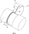
- FIG. 4 illustrates a schematic representation of a nacelle 400 with an open cowl access door 402 exposing an access opening 404.
- the nacelle 400 provides an annular housing within which a substantial portion of an aircraft engine is located.
- a nacelle 400 and access door 402 interface is illustrated as one embodiment, use in other locations of the nacelle 400 are also within the scope of the present disclosure.
- other examples including applications to different locations of the aircraft or other types of vehicles such as ships or other platforms and land-based applications are within the scope of the present disclosure.
- the access door 402 has an outer surface 406 and an inner surface 408 and, when closed, the outer surface 406 of the access door 402 is contiguous with the skin of the nacelle 400.
- EMI shielding 410a, 410b comprising the EBG structure 200 is shown in two locations; however, EMI shielding 410 may be provided on one of the two locations.
- the EMI shielding 410a is located on a deflector plate 412.
- the deflector plate 412 is made of conductive material.
- the deflector plate 412 is parallel to and recessed with respect to an outer surface 414 of the nacelle 400.
- the deflector plate 412 extends longitudinally from a radial interior surface 416 and is adjacent to the inner surface 408 of the access door 402.
- the EMI shielding 410a is connected to the deflector plate 412, such as with the aforementioned adhesive layer 302 or by other means, and extends circumferentially along the curved deflector plate 412 along one or more portion of the perimeter of the access opening 404. It is understood that the access door 402 may represent another panel, cover, window or the like and that the access opening 404 may represent any opening, aperture, slot or gap in the vehicle or platform.
- the EMI shielding 410b is located on the inner surface 408 of the access door 402 adjacent to the edge of the access door 402 and in opposing parallel juxtaposition to the deflector plate 412.
- the EMI shielding 410b extends along one or more portion of the perimeter of the access door 402.
- FIG. 4 shows the EMI shielding 410a, 410b located at the distal end of interface. EMI shielding 410a, 410b may also be employed at a proximal end and/or at lateral sides of the perimetral interface.
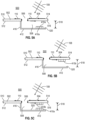
- FIG. 5A illustrates an electromagnetic wave 108 incident from an exterior 500 upon a vehicle section having EMI shielding 410a at an interface between an external first surface 502 and an external second surface 504 defining a gap 506
- the gap 506 may be very small but sufficient to permit a surface current 110 to flow around an edge to an interior 508.
- the external first surface 502 may be an aircraft skin having an outer surface 510 and an inner surface 512.
- the external second surface 504 may be a skin, nacelle access door, cover, window, panel, or the like, having an outer surface 514 and an inner surface 516.
- the external second surface 504 may be configured to cover or close an opening formed in the external first surface 502.
- a first perimeter is defined along the entire edge of the external first surface 502 and a second perimeter is defined along the entire edge of the external second surface 504.
- An interior surface 416 extends from the inner surface 512 of the external first surface 502 toward the interior 508. In one embodiment the interior surface 416 extends inwardly at the edge of at least a portion of the first perimeter. The interior surface 416 may be perpendicular to the external first surface 502 and, for a curved skin, the interior surface 416 will extend radially inwardly.
- a deflector plate 412 is connected to and extends laterally from the interior surface 416 extending below the gap 506 and below the external second surface 504. The deflector plate 412 may be parallel to the external second surface 504 defining a distance 518 therebetween.
- the distance 518 is constant and, if the external second surface 504 is curved, the deflector plate 412 is conformingly curved to maintain a constant distance 518 along the length and width of the deflector plate 412.
- the deflector plate 412 may extend along at least a portion of one or more edges of the first perimeter.
- the deflector plate 412 has a gap-facing surface 520 that faces the gap 506 and that faces the inner surface 516 of the external second surface 504.
- the EMI shielding 410a comprising the EBG structure 200 is attached to the gap-facing surface 520 of the deflector plate 412 via the adhesive layer 302 or by other means. A first edge of the EMI shielding 410a is laterally near the edge of the second perimeter.
- the second edge of the EMI shielding 410a terminates beneath the external second surface 504.
- the distance between the first edge and second edge of the EMI shielding 410 defines its width.
- the EMI shielding 410a extends along at least a portion of the length and width of the deflector plate 412. In one embodiment, the entire length and width of the EMI shielding 410a is positioned directly beneath the external second surface 504 such that the EMI shielding 410a is not located beneath the gap 506.
- FIG. 5B illustrates the same vehicle section as in FIG. 5A .
- the EMI shielding 410b is attached to the inner surface 516 of the external second surface 504 via the adhesive layer 302 or other means.
- the EMI shielding 410b is proximate to the gap 40 such that a first edge of the EMI shielding 410b is near or at the edge of the external second surface 504.
- a second edge of the EMI shielding 410b terminates opposite the deflector plate 412.
- the distance between the first and the second edge of the EMI shielding 410b defines its width.
- the EMI shielding 410b extends along at least a portion of the length and width of the external second surface 504 and along at least a portion of second perimeter.
- FIG. 5C illustrates the same vehicle section as in FIG. 5A .
- EMI shielding 410a, 410b is provided in both of the locations as described with respect to FIG. 5A and FIG. 5B .
- a first EMI shielding 410a is located on the deflector plate 412 and a second EMI shielding 410b is located on the external second surface 504.
- the first EMI shielding 410a is directly opposite and aligned with the second EMI shielding 410b.
- the first and second EMI shielding 410a, 410b are offset from each other.
- One of the first and second EMI shielding 410a, 410b may be longer than the other.
- the electromagnetic wave 108 incident upon the external surfaces 502, 504 will generate an electric surface current 110 along the metallic surface of the aircraft skin that will pass through the gap 506 to the interior 508 where sensitive avionics may be disrupted. Direct illumination of the gap 506 may result in a transmitted wave entering the interior 508.
- electromagnetic radiation is directed into the space between the external second surface 504 and the deflector plate 412 where it will encounter the EMI shielding 410a, 410b positioned in one of the three configurations described above.
- the EBG structure 200 incorporated into the EMI shielding 410 will block and attenuate transmission of the electromagnetic radiation further into the interior 508 protecting electronics located therein.
- electromagnetic radiation blockage is possible over a limited band gap frequency range.
- the separation distance between unit cells 202 acts as a capacitance to the oncoming wave, and the via 208 to ground 204 provides an inductance. When the inductance and capacitance are tuned, the wave sees high-surface impedance as in a band-stop filter.
- An EBG structure 200 is designed to block a set of modes of electric currents and magnetic fields propagating in a particular platform.
- the EBG structure 200 may consist of different unit cell 202 or block designs to synthesize an optimal filter performance.
- the deflector plate 412 converts impinging electromagnetic waves to form a parallel plate mode so that the EBG structure 200 filters out penetrating electromagnetic energy and prevents highly resonant cavity mode build-ups of electromagnetic energy inside the nacelle or other enclosure.
- the shielding assembly effectively prevents electromagnetic couplings through the open apertures.
- FIG. 6 illustrates a test case used to determine how well the EMI shielding assembly described herein performs.
- FIG. 6 is an electric field intensity map at a cross-section of a 3D cavity model having a deflector plate 412 with no EMI shielding 410 on the left side of FIG. 6 and EMI shielding 410a provided on the deflector plate 412, according to the assembly described with respect to FIG. 5A , on the right side of FIG. 6 .
- a 9x9 unit cell array EBG structure 200 was employed in the model under a plane wave illumination at a stop band frequency.
- electrical field intensity of approximately 1.0 V/m at the exterior of the assembly dropped to approximately 0.001 V/m at the interior.
- the EMI shielding assembly is effective at blocking surface waves from propagating over its band gap range of frequencies.
- the EBG unit cell 202 may be scaled in size to operate at any desired frequency band.
- primary EMI shielding 410a can be deployed together with secondary EMI shielding 410b as shown in FIG. 5C for higher filter attenuation levels.
- the EMI shielding 410 can be easily applied to any open aperture or slot functionally required in aircraft, ships, or other platforms that need efficient protection of on-board electronic/electrical systems against hostile irradiations.
- Example one includes an assembly for EMI shielding of an interior of an aircraft comprising a first external surface and a second external surface having an inner surface, the first external surface being contiguous with the second external surface and defining a gap therebetween, a deflector plate located in the interior, the deflector plate having a gap-facing surface parallel and adjacent to the inner surface of the second external surface, and a first shielding located on the gap-facing surface, the first shielding including a first electromagnetic band gap structure.
- Example two includes the assembly for EMI shielding of Example one and further comprises a second shielding located on the inner surface of the second external surface opposite from the first shielding, the second shielding including a second electromagnetic band gap structure.
- Example three includes the assembly for EMI shielding of Example one and further comprises an interior surface connected to the first external surface and extending toward the interior from the first external surface, the deflector plate being connected to the interior surface.
- Example four includes the assembly for EMI shielding of Example three, wherein the deflector plate is conductive and located beneath the gap and the second external surface.
- Example five includes the assembly for EMI shielding of Example one, wherein the electromagnetic band gap structure includes unit cells, each unit cell comprising a conductive patch and via connected to a ground layer.
- Example six includes the assembly for EMI shielding of Example one, wherein the electromagnetic band gap structure is configured to block electromagnetic radiation over a limited band gap frequency range.
- Example seven includes the assembly for EMI shielding of Example one, wherein the first shielding includes a conductive adhesive layer.
- Example eight includes the assembly for EMI shielding of Example one, wherein the first shielding includes a passivation layer along an outer surface of the electromagnetic band gap structure.
- Example nine includes the assembly for EMI shielding of Example one, wherein the interior is an interior of a nacelle and the second external surface is a nacelle access door.
- Example ten includes the assembly for EMI shielding of Example one and further includes avionics equipment in the interior.
- Example eleven includes the assembly for EMI shielding of Example one, wherein the gap-facing surface of the deflector plate and the inner surface of the second external surface define a distance therebetween configured to establish a parallel plate mode in electromagnetic waves entering the interior through the gap.
- Example twelve includes an assembly for EMI shielding of an interior of an aircraft comprising a first external surface and a second external surface having an inner surface, the first external surface being contiguous with the second external surface and defining a gap therebetween, a deflector plate located in the interior and having a gap-facing surface parallel to and opposite from the inner surface of the second external surface, and a first shielding located on the inner surface of the second external surface, the first shielding including a first electromagnetic band gap structure.
- Example thirteen includes the assembly for EMI shielding of Example twelve wherein the first shielding includes a first edge and a second edge defining a width of the first shielding, the first edge located near the gap and the second edge located distally from the gap.
- Example fourteen includes the assembly for EMI shielding of Example thirteen, wherein the first shielding includes a length perpendicular to the width, the length extending along at least a portion of a perimeter of the second external surface.
- Example fifteen includes the assembly for EMI shielding of Example fourteen, wherein the first shielding includes unit cells arrayed along the length and the width of the first shielding, each unit cell comprising a conductive patch and via connected to a ground layer and a dielectric substrate layer extending from the conductive patch to the ground layer.
- Example sixteen includes EMI shielding comprising an electromagnetic band gap structure including an array of unit cells across a length and a width, each unit cell comprising a flat conductive patch parallel to the length and width, each patch having an inner surface, and a conductive via connected to the inner surface of the patch, a conductive ground layer having an inner surface and an outer surface, the conductive via extending from the patch to the inner surface of ground layer, a substrate layer of dielectric material located between the patches and the ground layer, and a conductive adhesive layer connected to the outer surface of the ground layer.
- EMI shielding comprising an electromagnetic band gap structure including an array of unit cells across a length and a width, each unit cell comprising a flat conductive patch parallel to the length and width, each patch having an inner surface, and a conductive via connected to the inner surface of the patch, a conductive ground layer having an inner surface and an outer surface, the conductive via extending from the patch to the inner surface of ground layer, a substrate layer of dielectric material located between the patches and the ground layer, and
- Example seventeen includes the EMI shielding of Example sixteen, wherein the shielding is flexible.
- Example eighteen includes the EMI shielding of Example sixteen, wherein the patch has a polygonal shape.
- Example nineteen includes the EMI shielding of Example sixteen and further includes a passivation layer on a top surface of the electromagnetic band gap structure.
- Example twenty includes the EMI shielding of Example sixteen wherein the electromagnetic band gap structure is configured to block electromagnetic radiation over a limited band gap frequency range.
Landscapes
- Engineering & Computer Science (AREA)
- Microelectronics & Electronic Packaging (AREA)
- Physics & Mathematics (AREA)
- Electromagnetism (AREA)
- Optics & Photonics (AREA)
- Aviation & Aerospace Engineering (AREA)
- Shielding Devices Or Components To Electric Or Magnetic Fields (AREA)
Abstract
An assembly for electromagnetic interference (EMI) shielding to prevent incident radiation from penetrating through a gap to an interior of an aircraft comprises an electromagnetic band gap (EBG) structure. The EBG structure has a patch-and-via array connected to a ground layer. The EMI shielding includes a conductive adhesive and is flexible for conforming attachment to curved aircraft surfaces. The shielding may be located on a deflector plate that is parallel to an adjacent aircraft surface, on the airframe surface opposite to the deflector plate, or in both locations. The assembly filters out penetrating electromagnetic energy and prevents highly resonant cavity mode buildups of electromagnetic energy inside a nacelle or other enclosure effectively protecting electrical equipment in the interior.
Description
- This disclosure relates to aircraft and more particularly to improved protection of aircraft electronics against electromagnetic interference.
- Various electronic equipment is located inside throughout an aircraft. Some electronic equipment is located proximate to openings to the outside of the aircraft. These openings are closed with movable covers to provide access for service and repair. In some locations of the aircraft, the gaps around the openings are sealed and tightly covered. In other locations, narrow gaps and slots around the openings allow for thermal expansion and contraction, provide tolerance for mechanical vibration, and serve as locations for sensors and other systems. One such location is an aircraft nacelle. The nacelle, which houses the aircraft engine, turbine, and control electronics, has large access doors. Electronic equipment, such as a full authority digital engine controller (FADEC), in such locations is particularly susceptible to electromagnetic interference (EMI). EMI can penetrate gaps and can cause avionic equipment performance to degrade or even malfunction. EMI can come from various sources, both internal and external to the aircraft, such as lightning, solar flares, and electrostatic discharge. Also, one type of EMI is radio frequency interference (RFI). RFI sources external to the aircraft include high-intensity radiated field (HIRF) from radar, radio, television and other ground-based, shipborne or airborne radio frequency transmitters, electromagnetic pulse (EMP) and high power microwave (HPM) irradiation, all of which, can penetrate the aircraft at these gap locations and impact aircraft electronic systems. While protective conductive seals are currently used in the vicinity of gap locations, they are not effective against all possible electromagnetic penetrations and are also costly and troublesome to maintain. Therefore, improved and effective protection against EMI/RFI is needed.
- In accordance with one or more examples, an assembly for electromagnetic interference shielding of an interior of an aircraft includes the features described at claim 1. The dependent claims outline advantageous forms of embodiment of the assembly.
- The features, functions, and advantages that have been discussed can be achieved independently in various examples or may be combined in yet other examples further details of which can be seen with reference to the following description and drawings.
- The various advantages of the examples of the present disclosure will become apparent to one skilled in the art by reading the following specification and appended claims, and by referencing the following drawings in which:
-
FIG. 1 is a schematic diagram showing an aircraft section having an opening; -
FIG. 2A is a schematic diagram showing a top view of an electromagnetic band gap structure, according to one or more examples; -
FIG. 2B is a schematic diagram showing a side-elevational view of the electromagnetic band gap structure ofFIG. 2A , according to one or more examples; -
FIG. 3 is a schematic diagram showing a side-elevational view of an EMI shielding, according to one or more examples; -
FIG. 4 is a schematic diagram showing a top perspective view of an aircraft nacelle with access doors open and EMI shielding, according to one or more examples; -
FIG. 5A is a schematic diagram showing an aircraft section having an opening shielded with EMI shielding in a first location, according to one or more examples; -
FIG. 5B is a schematic diagram showing an aircraft section having an opening shielded with EMI shielding in a second location, according to one or more examples; -
FIG. 5C is a schematic diagram showing an aircraft section having an opening shielded with EMI shielding in a first and second location, according to one or more examples; and -
FIG. 6 is an electric field intensity map at a cross-section of a cavity model with no EMI shielding on the left side and with EMI shielding on the right side, according to one or more examples. - An assembly for EMI shielding to prevent incident radiation from penetrating through a gap to an interior of an aircraft comprises an electromagnetic band gap (EBG) structure. The EMI shielding may be located on interior airframe structures near gaps. The assembly filters out penetrating electromagnetic energy and prevents highly resonant cavity mode build-ups of electromagnetic energy inside a nacelle or other enclosure effectively protecting electrical equipment located in the interior.
-
FIG. 1 is a schematic diagram of an exemplary section of anaircraft skin 100 showing a firstexternal aircraft surface 102 and a secondexternal aircraft surface 104 defining agap 106 therebetween. Theaircraft skin 100 is made from aluminum or aluminum alloy.FIG. 1 illustrates twoexternal aircraft surfaces FIG. 1 may be any location on the surface of an aircraft or an interface location of the same material or different material. Theexemplary gap 106 is illustrative of any aperture, seam, joint, opening, orifice, slot or any other interface location found on an aircraft including but not limited to an aircraft body panel, an access door, a sensor aperture, a window, a port, a nacelle and cowl door. -
FIG. 1 illustrates aplane wave 108 incident upon theaircraft section 100 indirectly illuminating thegap 106 and generating asurface current 110 represented by the arrows. Thissurface current 110 will flow along anouter surface 112 of the firstexternal surface 102 and penetrate to aninterior 114 of the aircraft via thegap 106 and flow along aninner surface 116. Similarly, asurface current 110 will flow along anouter surface 118 of the secondexternal surface 104 and penetrate to theinterior 114 of the aircraft via thegap 106 and flow along aninner surface 120. The low impedance of the aluminum aircraft skin allows current to flow over the entire metal surface. The electromagnetic field levels inside theinterior 114 will increase as a result of surface current and any transmittedwave 122 penetration via thegap 106 and may cause interference with avionic systems that are located in theinterior 114. -
FIGs. 2A and 2B shows an electromagnetic band gap (EBG)structure 200. TheEBG structure 200 includesunit cells 202 repeated many times in a two-dimensional pattern to form a broadband high-impedance surface (HIS). Eachunit cell 202 includes a bottom metalground plane layer 204, ametal patch 206, and a conducting via 208 having a diameter, 2r, extending and interconnected between the two. Eachunit cell 202 forms a mushroom-like unit extending from the ground.FIG. 2A illustrates anEBG structure 200 having a 6x6 array ofunit cells 202. Any size array may be employed. Additionally, asubstrate 210 may be included between theground plane layer 204 and thepatch 206. Theground plane layer 204 inFIG. 2A is a common ground for all theunit cells 202. In another embodiment, theground plane layer 204 may be divided. Theground plane layer 204 can be made of any conductive metal such as aluminum or copper. Thepatch 206 is square having a side length of w; however, any suitable patch shape may be employed such as circular or polygonal. Thepatch 206 can be made of any conductive metal such as aluminum or copper. The dimensions of thepatch 206 are selected such that there is a specific separation distance, g, in between neighboringpatches 206 in all directions. Each unit cell's along-the-plane dimensions are a small fraction of a wavelength in an operating range in order for the surface as a whole to appear electromagnetically homogeneous.Exemplary unit cell 202 dimensions are approximately 1.0-10.0 mm for thepatch 206 length and width, w, approximately 0.1-5.0 mm for the separation distance, g, and approximately 3.0-15 mm for thesubstrate 210 thickness (patch height), h. Thesubstrate 210 may be made of a dielectric material having a dielectric constant εr of approximately 1.0-3.0. -
FIG. 3 illustrates theEBG structure 200 connected to a conductingairframe surface 300. TheEBG structure 200 includes anadhesive layer 302. Theadhesive layer 302 is conductive such that theground plane layer 204 can be electrically connected to a conductingairframe surface 300. Theadhesive layer 302 is configured such that theEBG structure 200 is electrically connected to theadhesive layer 302 which may be in the form of an adhesive tape having a conductive substrate backing with conductive adhesive arranged on two sides of the substrate backing with one side adhered to theground plane layer 204 and another side for adhering to anairframe surface 300. Any type of conventional, pressure-sensitive conductive adhesive or conductive adhesive tape may comprise theadhesive layer 302. In one embodiment of theEBG structure 200 that includes theadhesive layer 302, theEBG structure 200 is flexible so that it may be easily and conformingly attached to curved surfaces commonly found on airframe surfaces. TheEBG structure 200 is thin and flat and may be formed into a tape having dimensions suitable for a particular application. In one embodiment, the length is longer than its width and may be formed into a rolled strip for easy installation. TheEBG structure 200 may also include apassivation layer 304 along the outer surface adjacent to thepatches 206. Thepassivation layer 304 fills any gaps between thepatches 206 andsubstrate 210 and serves as a blanket layer that provides environmental protection for theEBG structure 200. -
FIG. 4 illustrates a schematic representation of anacelle 400 with an opencowl access door 402 exposing anaccess opening 404. Thenacelle 400 provides an annular housing within which a substantial portion of an aircraft engine is located. Although anacelle 400 andaccess door 402 interface is illustrated as one embodiment, use in other locations of thenacelle 400 are also within the scope of the present disclosure. Also, other examples including applications to different locations of the aircraft or other types of vehicles such as ships or other platforms and land-based applications are within the scope of the present disclosure. Theaccess door 402 has anouter surface 406 and aninner surface 408 and, when closed, theouter surface 406 of theaccess door 402 is contiguous with the skin of thenacelle 400. EMI shielding 410a, 410b comprising theEBG structure 200 is shown in two locations; however, EMI shielding 410 may be provided on one of the two locations. In a first location, the EMI shielding 410a is located on adeflector plate 412. Thedeflector plate 412 is made of conductive material. Thedeflector plate 412 is parallel to and recessed with respect to anouter surface 414 of thenacelle 400. Thedeflector plate 412 extends longitudinally from a radialinterior surface 416 and is adjacent to theinner surface 408 of theaccess door 402. TheEMI shielding 410a is connected to thedeflector plate 412, such as with the aforementionedadhesive layer 302 or by other means, and extends circumferentially along thecurved deflector plate 412 along one or more portion of the perimeter of theaccess opening 404. It is understood that theaccess door 402 may represent another panel, cover, window or the like and that the access opening 404 may represent any opening, aperture, slot or gap in the vehicle or platform. In a second location, the EMI shielding 410b is located on theinner surface 408 of theaccess door 402 adjacent to the edge of theaccess door 402 and in opposing parallel juxtaposition to thedeflector plate 412. The EMI shielding 410b extends along one or more portion of the perimeter of theaccess door 402.FIG. 4 shows the EMI shielding 410a, 410b located at the distal end of interface. EMI shielding 410a, 410b may also be employed at a proximal end and/or at lateral sides of the perimetral interface. -
FIG. 5A illustrates anelectromagnetic wave 108 incident from an exterior 500 upon a vehicle section having EMI shielding 410a at an interface between an externalfirst surface 502 and an externalsecond surface 504 defining agap 506 Thegap 506 may be very small but sufficient to permit a surface current 110 to flow around an edge to an interior 508. The externalfirst surface 502 may be an aircraft skin having anouter surface 510 and aninner surface 512. The externalsecond surface 504 may be a skin, nacelle access door, cover, window, panel, or the like, having anouter surface 514 and aninner surface 516. The externalsecond surface 504 may be configured to cover or close an opening formed in the externalfirst surface 502. A first perimeter is defined along the entire edge of the externalfirst surface 502 and a second perimeter is defined along the entire edge of the externalsecond surface 504. Aninterior surface 416 extends from theinner surface 512 of the externalfirst surface 502 toward the interior 508. In one embodiment theinterior surface 416 extends inwardly at the edge of at least a portion of the first perimeter. Theinterior surface 416 may be perpendicular to the externalfirst surface 502 and, for a curved skin, theinterior surface 416 will extend radially inwardly. Adeflector plate 412 is connected to and extends laterally from theinterior surface 416 extending below thegap 506 and below the externalsecond surface 504. Thedeflector plate 412 may be parallel to the externalsecond surface 504 defining adistance 518 therebetween. Thedistance 518 is constant and, if the externalsecond surface 504 is curved, thedeflector plate 412 is conformingly curved to maintain aconstant distance 518 along the length and width of thedeflector plate 412. Thedeflector plate 412 may extend along at least a portion of one or more edges of the first perimeter. Thedeflector plate 412 has a gap-facingsurface 520 that faces thegap 506 and that faces theinner surface 516 of the externalsecond surface 504. The EMI shielding 410a comprising theEBG structure 200 is attached to the gap-facingsurface 520 of thedeflector plate 412 via theadhesive layer 302 or by other means. A first edge of the EMI shielding 410a is laterally near the edge of the second perimeter. The second edge of the EMI shielding 410a terminates beneath the externalsecond surface 504. The distance between the first edge and second edge of the EMI shielding 410 defines its width. TheEMI shielding 410a extends along at least a portion of the length and width of thedeflector plate 412. In one embodiment, the entire length and width of the EMI shielding 410a is positioned directly beneath the externalsecond surface 504 such that the EMI shielding 410a is not located beneath thegap 506. -
FIG. 5B illustrates the same vehicle section as inFIG. 5A . In the embodiment ofFIG. 5B , the EMI shielding 410b is attached to theinner surface 516 of the externalsecond surface 504 via theadhesive layer 302 or other means. The EMI shielding 410b is proximate to the gap 40 such that a first edge of the EMI shielding 410b is near or at the edge of the externalsecond surface 504. In one embodiment, a second edge of the EMI shielding 410b terminates opposite thedeflector plate 412. The distance between the first and the second edge of the EMI shielding 410b defines its width. The EMI shielding 410b extends along at least a portion of the length and width of the externalsecond surface 504 and along at least a portion of second perimeter. -
FIG. 5C illustrates the same vehicle section as inFIG. 5A . In the embodiment ofFIG. 5C , EMI shielding 410a, 410b is provided in both of the locations as described with respect toFIG. 5A and FIG. 5B . A first EMI shielding 410a is located on thedeflector plate 412 and a second EMI shielding 410b is located on the externalsecond surface 504. In one embodiment, the first EMI shielding 410a is directly opposite and aligned with the second EMI shielding 410b. In another embodiment, the first and second EMI shielding 410a, 410b are offset from each other. One of the first and second EMI shielding 410a, 410b may be longer than the other. - The
electromagnetic wave 108 incident upon theexternal surfaces gap 506 to the interior 508 where sensitive avionics may be disrupted. Direct illumination of thegap 506 may result in a transmitted wave entering the interior 508. With the EMI shielding assembly described herein, electromagnetic radiation is directed into the space between the externalsecond surface 504 and thedeflector plate 412 where it will encounter the EMI shielding 410a, 410b positioned in one of the three configurations described above. TheEBG structure 200 incorporated into the EMI shielding 410 will block and attenuate transmission of the electromagnetic radiation further into the interior 508 protecting electronics located therein. For selected geometry combinations of separation distance, height, and via diameter, electromagnetic radiation blockage is possible over a limited band gap frequency range. The separation distance betweenunit cells 202 acts as a capacitance to the oncoming wave, and the via 208 toground 204 provides an inductance. When the inductance and capacitance are tuned, the wave sees high-surface impedance as in a band-stop filter. AnEBG structure 200 is designed to block a set of modes of electric currents and magnetic fields propagating in a particular platform. TheEBG structure 200 may consist ofdifferent unit cell 202 or block designs to synthesize an optimal filter performance. Thedeflector plate 412 converts impinging electromagnetic waves to form a parallel plate mode so that theEBG structure 200 filters out penetrating electromagnetic energy and prevents highly resonant cavity mode build-ups of electromagnetic energy inside the nacelle or other enclosure. The shielding assembly effectively prevents electromagnetic couplings through the open apertures. -
FIG. 6 illustrates a test case used to determine how well the EMI shielding assembly described herein performs.FIG. 6 is an electric field intensity map at a cross-section of a 3D cavity model having adeflector plate 412 with no EMI shielding 410 on the left side ofFIG. 6 and EMI shielding 410a provided on thedeflector plate 412, according to the assembly described with respect toFIG. 5A , on the right side ofFIG. 6 . A 9x9 unit cellarray EBG structure 200 was employed in the model under a plane wave illumination at a stop band frequency. As can be seen inFIG. 6 , electrical field intensity of approximately 1.0 V/m at the exterior of the assembly dropped to approximately 0.001 V/m at the interior. The EMI shielding assembly is effective at blocking surface waves from propagating over its band gap range of frequencies. TheEBG unit cell 202 may be scaled in size to operate at any desired frequency band. Also, primary EMI shielding 410a can be deployed together with secondary EMI shielding 410b as shown inFIG. 5C for higher filter attenuation levels. The EMI shielding 410 can be easily applied to any open aperture or slot functionally required in aircraft, ships, or other platforms that need efficient protection of on-board electronic/electrical systems against hostile irradiations. - Example one includes an assembly for EMI shielding of an interior of an aircraft comprising a first external surface and a second external surface having an inner surface, the first external surface being contiguous with the second external surface and defining a gap therebetween, a deflector plate located in the interior, the deflector plate having a gap-facing surface parallel and adjacent to the inner surface of the second external surface, and a first shielding located on the gap-facing surface, the first shielding including a first electromagnetic band gap structure.
- Example two includes the assembly for EMI shielding of Example one and further comprises a second shielding located on the inner surface of the second external surface opposite from the first shielding, the second shielding including a second electromagnetic band gap structure.
- Example three includes the assembly for EMI shielding of Example one and further comprises an interior surface connected to the first external surface and extending toward the interior from the first external surface, the deflector plate being connected to the interior surface.
- Example four includes the assembly for EMI shielding of Example three, wherein the deflector plate is conductive and located beneath the gap and the second external surface.
- Example five includes the assembly for EMI shielding of Example one, wherein the electromagnetic band gap structure includes unit cells, each unit cell comprising a conductive patch and via connected to a ground layer.
- Example six includes the assembly for EMI shielding of Example one, wherein the electromagnetic band gap structure is configured to block electromagnetic radiation over a limited band gap frequency range.
- Example seven includes the assembly for EMI shielding of Example one, wherein the first shielding includes a conductive adhesive layer.
- Example eight includes the assembly for EMI shielding of Example one, wherein the first shielding includes a passivation layer along an outer surface of the electromagnetic band gap structure.
- Example nine includes the assembly for EMI shielding of Example one, wherein the interior is an interior of a nacelle and the second external surface is a nacelle access door.
- Example ten includes the assembly for EMI shielding of Example one and further includes avionics equipment in the interior.
- Example eleven includes the assembly for EMI shielding of Example one, wherein the gap-facing surface of the deflector plate and the inner surface of the second external surface define a distance therebetween configured to establish a parallel plate mode in electromagnetic waves entering the interior through the gap.
- Example twelve includes an assembly for EMI shielding of an interior of an aircraft comprising a first external surface and a second external surface having an inner surface, the first external surface being contiguous with the second external surface and defining a gap therebetween, a deflector plate located in the interior and having a gap-facing surface parallel to and opposite from the inner surface of the second external surface, and a first shielding located on the inner surface of the second external surface, the first shielding including a first electromagnetic band gap structure.
- Example thirteen includes the assembly for EMI shielding of Example twelve wherein the first shielding includes a first edge and a second edge defining a width of the first shielding, the first edge located near the gap and the second edge located distally from the gap.
- Example fourteen includes the assembly for EMI shielding of Example thirteen, wherein the first shielding includes a length perpendicular to the width, the length extending along at least a portion of a perimeter of the second external surface.
- Example fifteen includes the assembly for EMI shielding of Example fourteen, wherein the first shielding includes unit cells arrayed along the length and the width of the first shielding, each unit cell comprising a conductive patch and via connected to a ground layer and a dielectric substrate layer extending from the conductive patch to the ground layer.
- Example sixteen includes EMI shielding comprising an electromagnetic band gap structure including an array of unit cells across a length and a width, each unit cell comprising a flat conductive patch parallel to the length and width, each patch having an inner surface, and a conductive via connected to the inner surface of the patch, a conductive ground layer having an inner surface and an outer surface, the conductive via extending from the patch to the inner surface of ground layer, a substrate layer of dielectric material located between the patches and the ground layer, and a conductive adhesive layer connected to the outer surface of the ground layer.
- Example seventeen includes the EMI shielding of Example sixteen, wherein the shielding is flexible.
- Example eighteen includes the EMI shielding of Example sixteen, wherein the patch has a polygonal shape.
- Example nineteen includes the EMI shielding of Example sixteen and further includes a passivation layer on a top surface of the electromagnetic band gap structure.
- Example twenty includes the EMI shielding of Example sixteen wherein the electromagnetic band gap structure is configured to block electromagnetic radiation over a limited band gap frequency range.
- Those skilled in the art will appreciate from the foregoing description that the broad techniques of the examples of the present disclosure can be implemented in a variety of forms. Therefore, while the examples of this disclosure have been described in connection with particular examples thereof, the true scope of the examples of the disclosure should not be so limited since other modifications will become apparent to the skilled practitioner upon a study of the drawings, specification, and following claims.
Claims (15)
- An assembly for electromagnetic interference shielding of an interior (508) of an aircraft, comprising:a first external surface (502) a second external surface (504) having an inner surface (516), the first external surface (502) being contiguous with the second external surface (504) and defining a gap (506) therebetween;a deflector plate (412) located in the interior (508), the deflector plate (412) having a gap-facing surface (520) parallel and opposite to the inner surface (516) of the second external surface (504); anda first shielding (410a) located on the gap-facing surface (520) of the deflector plate (412), the first shielding (410a) including a first electromagnetic band gap structure (200), and/or a second shielding (410b) located on the inner surface (516) of the second external surface (504), the second shielding (410b) including a second electromagnetic band gap structure (200).
- The assembly of claim 1, further comprising an interior surface (416) connected to the first external surface (502) and extending toward the interior (508) from the first external surface (502), the deflector plate (412) being connected to the interior surface (416).
- The assembly of any one of claims 1-2, wherein the deflector plate (412) is conductive and located beneath the gap (506) and the second external surface (504).
- The assembly of any one of the preceding claims, wherein the electromagnetic band gap structure (200) includes unit cells (202), each unit cell (202) comprising a conductive patch (206) and via (208) connected to a ground layer (204).
- The assembly of any one of the preceding claims, wherein the electromagnetic band gap structure (200) is configured to block electromagnetic radiation over a limited band gap frequency range.
- The assembly of any one of the preceding claims, wherein the first shielding (410a) and/or the second shielding (410b) include a conductive adhesive layer (302).
- The assembly of any one of the preceding claims, wherein the first shielding (410a) and/or the second shielding (410b) include a passivation layer (304) along an outer surface of the electromagnetic band gap structure (200).
- The assembly of any one of the preceding claims, wherein the interior (508) is an interior of a nacelle (400) and the second external surface (504) is a nacelle access door (402).
- The assembly of any one of the preceding claims, further including avionics equipment in the interior (508).
- The assembly of any one of the preceding claims, wherein the gap-facing surface (520) of the deflector plate (412) and the inner surface (516) of the second external surface (504) define a distance therebetween configured to establish a parallel plate mode in electromagnetic waves entering the interior through the gap (506).
- The assembly of any one of the preceding claims, wherein the first shielding (410a) and/or the second shielding (410b) include a first edge and a second edge defining a width of the first shielding (410a) and/or the second shielding (410b), the first edge located near the gap (506) and the second edge located distally from the gap (506).
- The assembly of any one of the preceding claims, wherein the first shielding (410a) and/or the second shielding (410b) include a length perpendicular to the width; the length extending along at least a portion of a perimeter of the second external surface (504) and/or along at least a portion of a perimeter of the deflector plate (412).
- The assembly of any one of the preceding claims, wherein the first shielding (410a) and/or the second shielding (410b) include unit cells (202) arrayed along the length and the width of the first shielding (410b), each unit cell (202) comprising a conductive patch (206) and via (208) connected to a ground layer (204) and a dielectric substrate layer (210) extending from the conductive patch (206) to the ground layer (204).
- The assembly of any one of the preceding claims, wherein the electromagnetic band gap structure (200) includes:an array of unit cells (202) across a length and a width, each unit cell (202) comprising:a flat conductive patch (206) parallel to the length and width; each patch (206) having an inner surface; anda conductive via (208) connected to the inner surface of the patch (206);a conductive ground layer (204) having an inner surface and an outer surface; the conductive via (208) extending from the patch (206) to the inner surface of ground layer (204);a substrate layer (210) of dielectric material located between the patches (206) and the ground layer (204); anda conductive adhesive layer (302) connected to the outer surface of the ground layer (204).
- The assembly of claim 14, wherein the structure (200) is flexible.
Applications Claiming Priority (1)
| Application Number | Priority Date | Filing Date | Title |
|---|---|---|---|
| US18/313,724 US12016164B1 (en) | 2023-05-08 | 2023-05-08 | RF filter device for aircraft nacelle access door gap |
Publications (1)
| Publication Number | Publication Date |
|---|---|
| EP4462971A1 true EP4462971A1 (en) | 2024-11-13 |
Family
ID=90365292
Family Applications (1)
| Application Number | Title | Priority Date | Filing Date |
|---|---|---|---|
| EP24163278.5A Pending EP4462971A1 (en) | 2023-05-08 | 2024-03-13 | Radio frequency filter for aircraft nacelle access door gap |
Country Status (3)
| Country | Link |
|---|---|
| US (1) | US12016164B1 (en) |
| EP (1) | EP4462971A1 (en) |
| CN (1) | CN118921974A (en) |
Citations (3)
| Publication number | Priority date | Publication date | Assignee | Title |
|---|---|---|---|---|
| US20130107491A1 (en) * | 2010-07-12 | 2013-05-02 | Masaharu Imazato | Electronic apparatus |
| US20140022139A1 (en) * | 2012-07-19 | 2014-01-23 | The Mitre Corporation | Conformal Electro-Textile Antenna and Electronic Band Gap Ground Plane for Suppression of Back Radiation From GPS Antennas Mounted on Aircraft |
| US20180277946A1 (en) * | 2017-03-24 | 2018-09-27 | Panasonic Corporation | Antenna apparatus |
Family Cites Families (5)
| Publication number | Priority date | Publication date | Assignee | Title |
|---|---|---|---|---|
| JPH098490A (en) * | 1995-06-21 | 1997-01-10 | Nippon Paint Co Ltd | Electronic device housing and unnecessary radiation wave reduction method |
| US8159832B2 (en) * | 2007-09-21 | 2012-04-17 | Nokia Corporation | Electromagnetic band gap structures and method for making same |
| US8013258B2 (en) * | 2008-06-11 | 2011-09-06 | Mediatek Inc. | Shielding device |
| US9515387B2 (en) * | 2012-08-17 | 2016-12-06 | Mediatek Inc. | Multi-input multi-output antenna with electromagnetic band-gap structure |
| CN113165339A (en) * | 2018-11-30 | 2021-07-23 | 积水化学工业株式会社 | Conductive nonwoven fabric |
-
2023
- 2023-05-08 US US18/313,724 patent/US12016164B1/en active Active
-
2024
- 2024-03-13 EP EP24163278.5A patent/EP4462971A1/en active Pending
- 2024-04-09 CN CN202410419314.9A patent/CN118921974A/en active Pending
Patent Citations (3)
| Publication number | Priority date | Publication date | Assignee | Title |
|---|---|---|---|---|
| US20130107491A1 (en) * | 2010-07-12 | 2013-05-02 | Masaharu Imazato | Electronic apparatus |
| US20140022139A1 (en) * | 2012-07-19 | 2014-01-23 | The Mitre Corporation | Conformal Electro-Textile Antenna and Electronic Band Gap Ground Plane for Suppression of Back Radiation From GPS Antennas Mounted on Aircraft |
| US20180277946A1 (en) * | 2017-03-24 | 2018-09-27 | Panasonic Corporation | Antenna apparatus |
Also Published As
| Publication number | Publication date |
|---|---|
| CN118921974A (en) | 2024-11-08 |
| US12016164B1 (en) | 2024-06-18 |
Similar Documents
| Publication | Publication Date | Title |
|---|---|---|
| US8159407B2 (en) | Radome with integrated plasma shutter | |
| US7212147B2 (en) | Method of agile reduction of radar cross section using electromagnetic channelization | |
| US9038949B2 (en) | Radio frequency shielding system | |
| US7837443B2 (en) | Wind turbine comprising enclosure structure formed as a Faraday cage | |
| US5861860A (en) | Protector for one or more electromagnetic sensors | |
| US6140575A (en) | Shielded electronic circuit assembly | |
| WO2018111394A1 (en) | Isolation barrier | |
| US12016164B1 (en) | RF filter device for aircraft nacelle access door gap | |
| EP1690440B1 (en) | Electronic apparatus and enclosure employing substantially co-planar portions with mating crenellations | |
| US11381002B2 (en) | Coating for the concealment of objects from the electromagnetic radiation of antennas | |
| Wang et al. | Study on capability verification test of electromagnetic pulse protection for aircraft | |
| JPS61290803A (en) | Microstrip antenna for automobile | |
| US5592186A (en) | Sectional filter assembly | |
| RU2596859C2 (en) | Agent reducing radar visibility of aircraft | |
| CN212963039U (en) | Unmanned aerial vehicle defense system | |
| US6262363B1 (en) | Electromagnetic shielding method and apparatus | |
| RU2742585C1 (en) | Motor vehicle equipped with an onboard radio-technical complex | |
| EP4723376A1 (en) | Frequency selective surface (fss) for radio altimeter 5g interference mitigation | |
| CN224205402U (en) | Control box with electromagnetic shielding structure | |
| KR102287830B1 (en) | Apparatus for electromagnetic shielding of penetration electromagnetic waves | |
| EP0902612B1 (en) | Seam structure for enclosures | |
| US20080136717A1 (en) | Electromagnetic compatability with window-choke rings | |
| US12027763B1 (en) | Shielding systems for a platform experiencing unplanned electromagnetic energy radiation | |
| JPS58201406A (en) | Radome | |
| Huang et al. | A Design of Pluggable High Power Microwave Protection Device in Waveguide |
Legal Events
| Date | Code | Title | Description |
|---|---|---|---|
| PUAI | Public reference made under article 153(3) epc to a published international application that has entered the european phase |
Free format text: ORIGINAL CODE: 0009012 |
|
| STAA | Information on the status of an ep patent application or granted ep patent |
Free format text: STATUS: THE APPLICATION HAS BEEN PUBLISHED |
|
| AK | Designated contracting states |
Kind code of ref document: A1 Designated state(s): AL AT BE BG CH CY CZ DE DK EE ES FI FR GB GR HR HU IE IS IT LI LT LU LV MC ME MK MT NL NO PL PT RO RS SE SI SK SM TR |
|
| STAA | Information on the status of an ep patent application or granted ep patent |
Free format text: STATUS: REQUEST FOR EXAMINATION WAS MADE |
|
| 17P | Request for examination filed |
Effective date: 20250414 |