US6140575A - Shielded electronic circuit assembly - Google Patents
Shielded electronic circuit assembly Download PDFInfo
- Publication number
- US6140575A US6140575A US08/959,607 US95960797A US6140575A US 6140575 A US6140575 A US 6140575A US 95960797 A US95960797 A US 95960797A US 6140575 A US6140575 A US 6140575A
- Authority
- US
- United States
- Prior art keywords
- enclosure
- circuit assembly
- sub
- conductive
- electronic
- Prior art date
- Legal status (The legal status is an assumption and is not a legal conclusion. Google has not performed a legal analysis and makes no representation as to the accuracy of the status listed.)
- Expired - Fee Related
Links
Images


Classifications
-
- H—ELECTRICITY
- H05—ELECTRIC TECHNIQUES NOT OTHERWISE PROVIDED FOR
- H05K—PRINTED CIRCUITS; CASINGS OR CONSTRUCTIONAL DETAILS OF ELECTRIC APPARATUS; MANUFACTURE OF ASSEMBLAGES OF ELECTRICAL COMPONENTS
- H05K9/00—Screening of apparatus or components against electric or magnetic fields
- H05K9/0007—Casings
- H05K9/0015—Gaskets or seals
-
- H—ELECTRICITY
- H05—ELECTRIC TECHNIQUES NOT OTHERWISE PROVIDED FOR
- H05K—PRINTED CIRCUITS; CASINGS OR CONSTRUCTIONAL DETAILS OF ELECTRIC APPARATUS; MANUFACTURE OF ASSEMBLAGES OF ELECTRICAL COMPONENTS
- H05K9/00—Screening of apparatus or components against electric or magnetic fields
- H05K9/0007—Casings
- H05K9/0045—Casings being rigid plastic containers having a coating of shielding material
Definitions
- the present invention relates to improvements in electromagnetic shielding and in particular to shielding of electrical circuit assemblies and subassemblies.
- Isolation of circuit components from electromagnetic interference is particularly important in communications equipment, such as cable modems, cellular telephone units and related relay-station equipment having components that operate in the 10 MHz to 4 GHz frequency range.
- the typical RF isolation shield for electronic components in such units consists of a rectangular metallic enclosure.
- typical shields are often pressure-fit with conductive gaskets, using a large number of screws or soldering.
- Metallic shields may be attached and grounded by soldering; however, soldering can significantly increase the manufacturing expense of the product. Furthermore, soldering may not be reliable, especially if the shield is to be removed and reattached for repair or replacement of circuit components. After reattachment, air gaps in the seal caused by the roughness of the solder from which the shield was removed may remain. Moreover, such shields may be difficult to unsolder and the unsoldering operation itself is risky, possibly causing heat damage to electronic components or delamination of portions of the assembly. Furthermore, the use of conductive gaskets and screws for attaching such shields is expensive and labor-intensive due to the large number of screws needed to prevent EMI leakage and provide an adequate seal.
- Circuits may be sensitive to electromagnetic interference for a variety of reasons, including high gain, operation at high frequencies, and the use of components and structures conducive to inductive or capacitive coupling. The same qualities also characterize circuits that emit offending high-frequency electromagnetic radiation.
- conductive material may be arranged in a complete conductive enclosure. The surface of the enclosure ideally is in close proximity to the surface of the circuit. Typical metal enclosures, however, are rectangular, the height of the enclosure being chosen to allow clearance for the tallest component on the circuit being shielded. Complex geometries are often avoided due to the relatively high cost of casting, soldering, welding, or machining such structures.
- shielding for electromagnetic interference purposes attenuates radiation at least by 50 to 60 dB over a frequency range from 10 MHz to 4.0 GHz or more.
- the shield ideally is substantially continuous and encloses the shielded circuits closely and completely, i.e., forming a closed, highly conductive enclosure.
- Electromagnetic shielding for attenuating electromagnetic interference typically has a resistivity of 0.57 m ⁇ /mm 2 .
- the shield it would also be advantageous for the shield to allow the circuit assembly to be easily and repeatably accessed by opening the shield enclosure, without compromising the integrity of the closed shield.
- the shielded electronic circuit assembly comprises an enclosure and an electronic circuit assembly.
- the enclosure is formed of a composite material comprised of a nonmetallic structural material and a conductive material.
- the enclosure closes along a perimeter so as to provide conductive contact along the perimeter, surrounding the electronic circuit assembly and providing shielding from electromagnetic interference.
- the enclosure is conductively coupled to ground.
- the shielded electronic circuit assembly comprises a structural nonmetallic material and a conductive material, the conductive material providing electromagnetic-interference shielding.
- the structural nonmetallic material and the conductive material form an enclosure surrounding an electronic circuit assembly.
- the enclosure includes a top portion, a bottom portion, and a closing mechanism holding the top portion in conductive contact with the bottom portion.
- the enclosure further contains at least one opening through which conductive wires can pass, allowing electronic signals to be input to and output from the electronic circuit assembly.
- the enclosure is conductively coupled to ground.
- the shielded electronic circuit assembly comprises a structural nonmetallic material and a conductive material.
- the conductive material provides electromagnetic interference shielding.
- the structural nonmetallic material and the conductive material form an enclosure surrounding an electronic tuner assembly.
- the enclosure includes a top portion, a bottom portion, and a locking mechanism allowing the top portion to be held in conductive contact with the bottom portion.
- the enclosure further contains at least one opening through which conductive wires can pass, allowing electronic signals to be input to and output from the electronic tuner assembly.
- a mounting bracket is coupled to the enclosure. The bracket couples the electronic tuner assembly to the enclosure such that the conductive material does not short-circuit the electronic tuner assembly.
- the shape of the enclosure matches the shape of the electronic tuner assembly, so that a small insulating gap is maintained between the inside surface of the enclosure and the surface of the electronic tuner assembly.
- the enclosure reduces electromagnetic interference by at least 60 dB over a frequency range from 10 MHz to 4 GHz and the enclosure is conductively coupled to ground.
- FIG. 1A is a top plan view of an embodiment of the shielded electronic circuit assembly of the present invention.
- FIG. 1B is a cross-section view of an embodiment of the shielded electronic circuit assembly of the present invention along line 1--1 of FIG. 1A.
- FIG. 1C is a side elevation view facing the hinged edge of an embodiment of the shielded electronic circuit assembly of the present invention.
- FIG. 1D is a top plan view of the bottom portion of the electronic shielding enclosure of an embodiment of the present invention.
- FIG. 2 is a schematic representation of an embodiment of the present invention in which the shielded electronic circuit assembly is implemented within a cable modem.
- FIG. 1A a top plan view of an embodiment of the shielded electronic circuit assembly of the present invention is shown.
- a shielding material described below, is molded or shaped by well-known methods into an electromagnetic isolation shield enclosure 100, as shown in FIGS. 1A, 1B, 1C and 1D.
- Enclosure 100 is comprised of bottom portion 104, top portion 102, and hinges 114 positioned along hinged-edge 116 of enclosure 100.
- Enclosure 100 is shaped to contain circuit assembly 132, leaving only a small insulating gap between edge 138 of enclosure 100 and the edge of circuit assembly 132.
- Circuit assembly 132 can, for example, be a cable modem tuner or other electronic circuit device.
- Hinges 114 are constructed to allow top portion 102 of enclosure 100 to be folded over circuit assembly 132 and conductively fastened to bottom portion 104 along perimeter 138, thereby completely surrounding circuit assembly 132 with electromagnetic isolation shield enclosure 100.
- the shielding material can be comprised of a composite material formed of an insulating polymer or plastic embedded with a conductive material in the form of a mesh or coupled fiber network or the like.
- the composite material is sufficiently rigid to hold form and support circuit assembly 132, while being easily produced in complex shapes so as to allow the shape of enclosure 100 to closely match that of circuit assembly 132, and further allowing the formation of sub-enclosures to isolate subregions of circuit assembly 132.
- the structural material is also flexible enough to ensure that it can fasten around its perimeter over the circuit assembly without requiring expensive manufacturing tolerances.
- the embedded conductive material is cross-linked and sufficiently dense to provide a resistivity of 0.57 ⁇ m ⁇ /mm 2 or not more than 0.75 m ⁇ /mm 2 .
- the composite material can be laminated or coated on one or both sides, using well-known methods, with a conductive material such as aluminum, copper, silver, gold, or other conductive material to increase the conductivity and shielding effectiveness of the composite material.
- the shielding material can comprise a nonembedded polymer or plastic material laminated or coated with a conductive material.
- the composite material consists of a polyvinylchloride (PVC) or polyester structural material.
- PVC polyvinylchloride
- polyester structural material The PVC or polyester structure is coated on the inside with a urethane binder embedded with a conductive copper/silver material.
- FIG. 1D the top plan view of bottom portion 104 of electronic shielding enclosure 100 of an embodiment of the present invention is shown.
- Comer mounting brackets 134, and side mounting brackets 138, for mounting circuit assembly 132 in bottom portion 104 of enclosure 100 are also shown.
- Mounting brackets 134 include a securing means, not shown, which can be screws, pins, snap locks, epoxy, hooks, or other securing means to securely mount circuit assembly 132 to bottom portion 104 of enclosure 100.
- Mounting brackets 134 and 138 are designed to secure circuit assembly 132 so that an insulating gap is maintained between circuit assembly 132 and enclosure 100, thus preventing a short circuit of circuit assembly 132.
- mounting brackets 132 and 134 are possible including a single continuous mounting bracket positioned around the perimeter of bottom portion 104, multiple posts within bottom portion 104 away from the perimeter, or other configurations. These configurations are within the scope of the present invention.
- openings 110 are positioned on hinged-edge 116 to allow wires 112 to pass through enclosure 100. Openings for wire clearance may be generous in size or may take the form of one or several large openings through which multiple wires may pass.
- Wires 112 can be comprised of any type of conductive material, including leads, pins, and the like, and are used to transmit signals to and from circuit assembly 132. Wires 112 are insulated so that they do not make conductive contact with enclosure 100.
- Openings 110 also serve to provide airflow and cooling of enclosure 100. Additional openings may be added to increase airflow and cooling.
- Circuit assembly 132 contains sub-isolation regions 142, 144, 146, and 148. Each region is surrounded by a portion of ground trace 118. Gaps in the surrounding ground trace allow for non-grounded traces to provide input and output lines for sub-isolation regions 142, 144, 146, and 148.
- enclosure 100 is folded closed along hinges 114, walls 122 of top portion 102 are pressed against ground trace 118, providing conductive contact between ground trace 118 and walls 122 of enclosure 100.
- each sub-isolation region 142, 144, 146, and 148 is surrounded by a corresponding sub-enclosure 150, 120, 152, and 154.
- the sub-enclosures provide electromagnetic shielding for the sub-isolation regions.
- the flexibility of the composite material comprising enclosure 100 allows for walls 122 to press firmly against ground trace 118 when enclosure 100 is closed. Walls 122 can thus form a tight conductive seal with ground trace 118. Additionally, an elastomeric bead, not shown, can be placed along ground trace 118.
- the elastomeric bead is comprised of a compressible conductive material which bridges any gaps to ensure that a consistent, tight conductive seal is maintained between walls 122 and ground trace 118.
- the elastomeric bead can be formed of a variety of materials, such as PVC, polyester, or the like.
- a compression fit or interlocked joint may be used.
- a conductive metal bar 124 is mounted to ground trace 118 along hinged-edge 114.
- Bar 124 provides conductive contact to ground trace 118 and protrudes through enclosure 100 at three places evenly spaced along hinged-edge 116.
- Protruding regions of bar 124 provide a structural mount for securely attaching enclosure 100 and circuit assembly 132 within a larger electronic device such as a cable modem.
- the protruding regions of bar 124 are also coupled to ground, so as to provide solid grounding for ground trace 118.
- Enclosure 100 folds closed along hinges 114 and locks shut by the mating of locking snaps 106 along edge 140 of top portion 102 with holes 108 along edge 138 of bottom portion 104.
- An elastomeric bead as described above, can also be compressed between edges 138 and 140 to provide a consistent, tight, conductive seal between top portion 102 and bottom portion 104 of enclosure 100.
- the snaps 106 are locked into holes 108 by applying pressure, thus allowing simple inexpensive assembly without the risk of heat damage to circuit assembly 132.
- the snap locks 106 can easily be unlocked, providing easy access to circuit assembly 132.
- Other locking mechanisms such as clamps, screws, latches and the like, can be used to conductively couple edges 138 and 140, and are covered within the scope of the present invention.
- FIG. 1B a cross-sectional view of an embodiment of the shielded electronic circuit assembly of the present invention along line 1--1 of FIG. 1A is shown.
- Enclosure 100 is molded so that top portion 102 conforms to or matches the surface of circuit assembly 132, leaving an insulating gap between the inner surface of top portion 102 and the outer surface of circuit assembly 132.
- the size of the insulating gap is just large enough to prevent enclosure 100 from short-circuiting circuit assembly 132.
- a typical gap size is 5 mm or less; however, a considerably larger gap size can be used depending on a variety of factors, including the degree of shielding required and the operating frequency of the circuit.
- Edge 140 of top portion 102 is conductively coupled to edge 138 of bottom portion 104. Edge 140 bends slightly upward at a distal end and flattens out to form wall 122 which is in conductive contact with ground trace 118. Wall 122 bends upward and flattens to cap sub-enclosure 120 of sub-isolation region 144. Top portion 102 then bends down to form wall 122, conductively contacting ground trace 118 and surrounding circuit component 128 in sub-isolation region 144.
- Circuit component 128 can be a single-circuit component or a plurality of components. Furthermore, circuit component 128 can have a more complex geometry, requiring more contours in top portion 102 in order to maintain an insulating gap between top portion 102 and circuit assembly 132.
- Top portion 102 bends upward from wall 122 on the distal end of sub-enclosure 120 to form the cap of sub-enclosure 152. Top portion 102 then bends down to form wall 122 on the distal end of sub-enclosure 152 which is in conductive contact with ground trace 118. Thus sub-isolation region 146 is surrounded by sub-enclosure 152. Sub-enclosure 152 is shaped so as to maintain an insulating gap between top portion 102 and circuit assembly 132. Sub-enclosure 152 can be of varied and complex shape to accommodate the circuit component or components found in sub-isolation region 146.
- Top portion 102 then bends upward and flattens coupling at top hinge 114 to hinged edge 116, forming an additional sub-enclosure surrounding bar 124.
- Hinged-edge 116 is coupled to bottom portion at bottom hinge 114 to bottom portion 104 which extends underneath circuit assembly 132, bending up at the proximal end to form edge 138.
- enclosure 100 helps to provide improved shielding over a wider range of frequencies than would a rectangular-geometry shield in which the height of the shield is determined by the height of the tallest components on circuit assembly 132.
- sub-enclosure of sub-isolation regions 144 and 146 provides additional protection against interference between circuit elements within these regions.
- FIG. 1C a side elevation view facing the hinged edge of an embodiment of the shielded electronic circuit assembly of the present invention is shown. Holes 100 for wires 112 on hinged-edge 116 of enclosure 100 are shown, along with mounting bar 124 protruding from hinged-edge 116 in three places as described above.
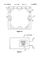
- FIG. 2 a schematic representation of an embodiment of the present invention in which the shielded electronic circuit assembly is implemented within a cable modem 200 is shown.
- Leads 202 and 204 provide input and output signals to cable modem 200.
- Enclosed within cable modem 200 is shielded electronic tuner assembly 206.
Abstract
Description
Claims (31)
Priority Applications (1)
| Application Number | Priority Date | Filing Date | Title |
|---|---|---|---|
| US08/959,607 US6140575A (en) | 1997-10-28 | 1997-10-28 | Shielded electronic circuit assembly |
Applications Claiming Priority (1)
| Application Number | Priority Date | Filing Date | Title |
|---|---|---|---|
| US08/959,607 US6140575A (en) | 1997-10-28 | 1997-10-28 | Shielded electronic circuit assembly |
Publications (1)
| Publication Number | Publication Date |
|---|---|
| US6140575A true US6140575A (en) | 2000-10-31 |
Family
ID=25502205
Family Applications (1)
| Application Number | Title | Priority Date | Filing Date |
|---|---|---|---|
| US08/959,607 Expired - Fee Related US6140575A (en) | 1997-10-28 | 1997-10-28 | Shielded electronic circuit assembly |
Country Status (1)
| Country | Link |
|---|---|
| US (1) | US6140575A (en) |
Cited By (17)
| Publication number | Priority date | Publication date | Assignee | Title |
|---|---|---|---|---|
| US20010033478A1 (en) * | 2000-04-21 | 2001-10-25 | Shielding For Electronics, Inc. | EMI and RFI shielding for printed circuit boards |
| DE10134152A1 (en) * | 2001-07-13 | 2003-01-30 | Knorr Bremse Systeme | Microprocessor controller has cover with constriction near microprocessor |
| EP1311146A2 (en) * | 2001-11-07 | 2003-05-14 | Alcatel | Electrical shield |
| US20040048077A1 (en) * | 1994-06-06 | 2004-03-11 | Shielding For Electronis, Inc. | Electromagnetic interference shield for electronic devices |
| US6706964B2 (en) * | 2001-09-04 | 2004-03-16 | Konica Corporation | Electronic device and method for manufacturing the same, and method for shielding printed circuit board |
| US6711032B2 (en) * | 2001-11-20 | 2004-03-23 | Mitsubishi Wireless Communications, Inc. | Shield and method for shielding an electronic device |
| US20040185280A1 (en) * | 2003-03-17 | 2004-09-23 | Pioneer Corporation | Heat-resistant insulating film and insulating method |
| US20040234752A1 (en) * | 2000-09-18 | 2004-11-25 | Wavezero, Inc. | Multi-layered structures and methods for manufacturing the multi-layered structures |
| US20050237663A1 (en) * | 2004-04-21 | 2005-10-27 | Riospring, Inc. | Insulator with pocket features |
| US20060154526A1 (en) * | 2005-01-07 | 2006-07-13 | Funai Electric Co., Ltd. | Printed circuit board and electronic apparatus equipped with the same |
| CN1295951C (en) * | 2002-04-23 | 2007-01-17 | 日本电气株式会社 | Electromagnetically shielded circuit device and shielding method therefor |
| CN100341389C (en) * | 2001-02-26 | 2007-10-03 | 戈尔企业控股股份有限公司 | Removable electromagnetic interference shield |
| US20080055878A1 (en) * | 2006-08-29 | 2008-03-06 | Texas Instruments Incorporated | Radiofrequency and electromagnetic interference shielding |
| EP2474770A1 (en) * | 2011-01-11 | 2012-07-11 | PII Limited | Apparatus for pipeline inspection |
| US20140247565A1 (en) * | 2013-03-01 | 2014-09-04 | Seiko Epson Corporation | Module, electronic apparatus and moving object |
| US20150070851A1 (en) * | 2013-09-12 | 2015-03-12 | Taiyo Yuden Co., Ltd. | Circuit module and method of producing the same |
| US20210137327A1 (en) * | 2019-11-13 | 2021-05-13 | Emerson Electric Co. | Vacuum cleaner motor assemblies and methods of operating same |
Citations (16)
| Publication number | Priority date | Publication date | Assignee | Title |
|---|---|---|---|---|
| US4037009A (en) * | 1976-08-11 | 1977-07-19 | Metex Corporation | Conductive elastomeric elements |
| US4384165A (en) * | 1981-09-14 | 1983-05-17 | Motorola, Inc. | Radio frequency shield with force multiplier interconnection fingers for an electromagnetic gasket |
| US4658334A (en) * | 1986-03-19 | 1987-04-14 | Rca Corporation | RF signal shielding enclosure of electronic systems |
| US4853790A (en) * | 1988-05-05 | 1989-08-01 | Dickie Robert G | Electromagnetic and electrostatic shielding for electronic equipment |
| US5068493A (en) * | 1988-11-10 | 1991-11-26 | Vanguard Products Corporation | Dual elastomer gasket shield for electronic equipment |
| US5072070A (en) * | 1989-12-01 | 1991-12-10 | Peter J. Balsells | Device for sealing electromagnetic waves |
| US5105056A (en) * | 1990-10-26 | 1992-04-14 | Schlegel Corporation | Electromagentic shielding with discontinuous adhesive |
| US5141770A (en) * | 1988-11-10 | 1992-08-25 | Vanguard Products Corporation | Method of making dual elastomer gasket shield for electromagnetic shielding |
| US5196712A (en) * | 1991-12-20 | 1993-03-23 | Raynet Corporation | Printed circuit board apparatus with optical switching |
| US5311408A (en) * | 1991-08-09 | 1994-05-10 | Tandem Computers, Incorporated | Electronic assembly with improved grounding and EMI shielding |
| US5414597A (en) * | 1994-05-04 | 1995-05-09 | Ford Motor Company | Shielded circuit module |
| US5473111A (en) * | 1992-10-07 | 1995-12-05 | Mitsubishi Denki Kabushiki Kaisha | Shielded enclosure for housing electronic components and manufacturing method thereof |
| US5557063A (en) * | 1994-01-03 | 1996-09-17 | Lucent Technologies Inc. | Electronic component enclosure for RF shielding |
| US5559677A (en) * | 1994-04-29 | 1996-09-24 | Motorola, Inc. | Method of forming a device by selectively thermal spraying a metallic conductive material thereon |
| US5586011A (en) * | 1994-08-29 | 1996-12-17 | At&T Global Information Solutions Company | Side plated electromagnetic interference shield strip for a printed circuit board |
| US5597979A (en) * | 1995-05-12 | 1997-01-28 | Schlegel Corporation | EMI shielding having flexible condustive sheet and I/O Gasket |
-
1997
- 1997-10-28 US US08/959,607 patent/US6140575A/en not_active Expired - Fee Related
Patent Citations (16)
| Publication number | Priority date | Publication date | Assignee | Title |
|---|---|---|---|---|
| US4037009A (en) * | 1976-08-11 | 1977-07-19 | Metex Corporation | Conductive elastomeric elements |
| US4384165A (en) * | 1981-09-14 | 1983-05-17 | Motorola, Inc. | Radio frequency shield with force multiplier interconnection fingers for an electromagnetic gasket |
| US4658334A (en) * | 1986-03-19 | 1987-04-14 | Rca Corporation | RF signal shielding enclosure of electronic systems |
| US4853790A (en) * | 1988-05-05 | 1989-08-01 | Dickie Robert G | Electromagnetic and electrostatic shielding for electronic equipment |
| US5068493A (en) * | 1988-11-10 | 1991-11-26 | Vanguard Products Corporation | Dual elastomer gasket shield for electronic equipment |
| US5141770A (en) * | 1988-11-10 | 1992-08-25 | Vanguard Products Corporation | Method of making dual elastomer gasket shield for electromagnetic shielding |
| US5072070A (en) * | 1989-12-01 | 1991-12-10 | Peter J. Balsells | Device for sealing electromagnetic waves |
| US5105056A (en) * | 1990-10-26 | 1992-04-14 | Schlegel Corporation | Electromagentic shielding with discontinuous adhesive |
| US5311408A (en) * | 1991-08-09 | 1994-05-10 | Tandem Computers, Incorporated | Electronic assembly with improved grounding and EMI shielding |
| US5196712A (en) * | 1991-12-20 | 1993-03-23 | Raynet Corporation | Printed circuit board apparatus with optical switching |
| US5473111A (en) * | 1992-10-07 | 1995-12-05 | Mitsubishi Denki Kabushiki Kaisha | Shielded enclosure for housing electronic components and manufacturing method thereof |
| US5557063A (en) * | 1994-01-03 | 1996-09-17 | Lucent Technologies Inc. | Electronic component enclosure for RF shielding |
| US5559677A (en) * | 1994-04-29 | 1996-09-24 | Motorola, Inc. | Method of forming a device by selectively thermal spraying a metallic conductive material thereon |
| US5414597A (en) * | 1994-05-04 | 1995-05-09 | Ford Motor Company | Shielded circuit module |
| US5586011A (en) * | 1994-08-29 | 1996-12-17 | At&T Global Information Solutions Company | Side plated electromagnetic interference shield strip for a printed circuit board |
| US5597979A (en) * | 1995-05-12 | 1997-01-28 | Schlegel Corporation | EMI shielding having flexible condustive sheet and I/O Gasket |
Cited By (26)
| Publication number | Priority date | Publication date | Assignee | Title |
|---|---|---|---|---|
| US20040048077A1 (en) * | 1994-06-06 | 2004-03-11 | Shielding For Electronis, Inc. | Electromagnetic interference shield for electronic devices |
| US7358447B2 (en) | 1994-06-06 | 2008-04-15 | Wavezero, Inc. | Electromagnetic interference shields for electronic devices |
| US20070199738A1 (en) * | 1994-06-06 | 2007-08-30 | Wavezero, Inc. | Electromagnetic Interference Shields for Electronic Devices |
| US20010033478A1 (en) * | 2000-04-21 | 2001-10-25 | Shielding For Electronics, Inc. | EMI and RFI shielding for printed circuit boards |
| WO2001082672A1 (en) * | 2000-04-21 | 2001-11-01 | Shielding For Electronics, Inc. | Emi and rfi shielding for printed circuit boards |
| US20040234752A1 (en) * | 2000-09-18 | 2004-11-25 | Wavezero, Inc. | Multi-layered structures and methods for manufacturing the multi-layered structures |
| CN100341389C (en) * | 2001-02-26 | 2007-10-03 | 戈尔企业控股股份有限公司 | Removable electromagnetic interference shield |
| DE10134152A1 (en) * | 2001-07-13 | 2003-01-30 | Knorr Bremse Systeme | Microprocessor controller has cover with constriction near microprocessor |
| US6706964B2 (en) * | 2001-09-04 | 2004-03-16 | Konica Corporation | Electronic device and method for manufacturing the same, and method for shielding printed circuit board |
| EP1311146A2 (en) * | 2001-11-07 | 2003-05-14 | Alcatel | Electrical shield |
| EP1311146A3 (en) * | 2001-11-07 | 2005-11-23 | Alcatel | Electrical shield |
| US6711032B2 (en) * | 2001-11-20 | 2004-03-23 | Mitsubishi Wireless Communications, Inc. | Shield and method for shielding an electronic device |
| CN1295951C (en) * | 2002-04-23 | 2007-01-17 | 日本电气株式会社 | Electromagnetically shielded circuit device and shielding method therefor |
| US20040185280A1 (en) * | 2003-03-17 | 2004-09-23 | Pioneer Corporation | Heat-resistant insulating film and insulating method |
| US20050237663A1 (en) * | 2004-04-21 | 2005-10-27 | Riospring, Inc. | Insulator with pocket features |
| US20060154526A1 (en) * | 2005-01-07 | 2006-07-13 | Funai Electric Co., Ltd. | Printed circuit board and electronic apparatus equipped with the same |
| US20080055878A1 (en) * | 2006-08-29 | 2008-03-06 | Texas Instruments Incorporated | Radiofrequency and electromagnetic interference shielding |
| US8004860B2 (en) * | 2006-08-29 | 2011-08-23 | Texas Instruments Incorporated | Radiofrequency and electromagnetic interference shielding |
| EP2474770A1 (en) * | 2011-01-11 | 2012-07-11 | PII Limited | Apparatus for pipeline inspection |
| US20140247565A1 (en) * | 2013-03-01 | 2014-09-04 | Seiko Epson Corporation | Module, electronic apparatus and moving object |
| US9426892B2 (en) * | 2013-03-01 | 2016-08-23 | Seiko Epson Corporation | Module, electronic apparatus and moving object |
| US20150070851A1 (en) * | 2013-09-12 | 2015-03-12 | Taiyo Yuden Co., Ltd. | Circuit module and method of producing the same |
| US9807916B2 (en) * | 2013-09-12 | 2017-10-31 | Taiyo Yuden Co., Ltd. | Circuit module and method of producing the same |
| US20210137327A1 (en) * | 2019-11-13 | 2021-05-13 | Emerson Electric Co. | Vacuum cleaner motor assemblies and methods of operating same |
| US11647878B2 (en) | 2019-11-13 | 2023-05-16 | Emerson Electric Co. | Vacuum cleaner motor assemblies and methods of operating same |
| US11672390B2 (en) * | 2019-11-13 | 2023-06-13 | Emerson Electric Co. | Vacuum cleaner motor assemblies and methods of operating same |
Similar Documents
| Publication | Publication Date | Title |
|---|---|---|
| US6140575A (en) | Shielded electronic circuit assembly | |
| EP0729294B1 (en) | Arrangement for preventing eletromagnetic interference | |
| US5266054A (en) | Sealed and filtered header receptacle | |
| US4829432A (en) | Apparatus for shielding an electrical circuit from electromagnetic interference | |
| US5899755A (en) | Integrated circuit test socket with enhanced noise imminity | |
| US5597979A (en) | EMI shielding having flexible condustive sheet and I/O Gasket | |
| AU674454B2 (en) | EMI shielding having flexible conductive envelope | |
| US5557063A (en) | Electronic component enclosure for RF shielding | |
| CN102820590A (en) | Integrated connector shield ring for shielded enclosures | |
| US5748449A (en) | Electrical enclosure for radio | |
| JP3208076B2 (en) | Shield case | |
| JP4282473B2 (en) | Shield assembly for connector and connector assembly | |
| US6243274B1 (en) | Shields for electronic components with ready access to shielded components | |
| US5610368A (en) | Clip plate bulkhead mounting for EMI filters | |
| JP3112825B2 (en) | Microwave equipment | |
| JPH08204377A (en) | Shielding body | |
| CA2015756A1 (en) | Shielded electrical connector | |
| FI91931B (en) | An EMC enclosure | |
| US6188017B1 (en) | Electromagnetic interference (EMI) shielding apparatus | |
| KR19990077109A (en) | Protection against electronic connection and electrostatic discharge | |
| JP3815528B2 (en) | Electronics | |
| US6775154B1 (en) | Electromagnetic baffle for printed circuit boards | |
| JP3447436B2 (en) | EMI Countermeasure Package Equipment | |
| JP3346510B2 (en) | Board connector and shield shell used for it | |
| JPS58123201A (en) | Shield structure of microwave circuit |
Legal Events
| Date | Code | Title | Description |
|---|---|---|---|
| AS | Assignment |
Owner name: 3COM CORPORATION, CALIFORNIA Free format text: ASSIGNMENT OF ASSIGNORS INTEREST;ASSIGNOR:VAN GUNTEN, LAMAR;REEL/FRAME:008799/0062 Effective date: 19970923 Owner name: 3COM CORPORATION, CALIFORNIA Free format text: ASSIGNMENT OF ASSIGNORS INTEREST;ASSIGNOR:PATEL, SANDEEP;REEL/FRAME:008798/0892 Effective date: 19971024 |
|
| FPAY | Fee payment |
Year of fee payment: 4 |
|
| FEPP | Fee payment procedure |
Free format text: PAYOR NUMBER ASSIGNED (ORIGINAL EVENT CODE: ASPN); ENTITY STATUS OF PATENT OWNER: LARGE ENTITY Free format text: PAYER NUMBER DE-ASSIGNED (ORIGINAL EVENT CODE: RMPN); ENTITY STATUS OF PATENT OWNER: LARGE ENTITY |
|
| FPAY | Fee payment |
Year of fee payment: 8 |
|
| REMI | Maintenance fee reminder mailed | ||
| AS | Assignment |
Owner name: HEWLETT-PACKARD COMPANY, CALIFORNIA Free format text: MERGER;ASSIGNOR:3COM CORPORATION;REEL/FRAME:024630/0820 Effective date: 20100428 |
|
| AS | Assignment |
Owner name: HEWLETT-PACKARD COMPANY, CALIFORNIA Free format text: CORRECTIVE ASSIGNMENT TO CORRECT THE SEE ATTACHED;ASSIGNOR:3COM CORPORATION;REEL/FRAME:025039/0844 Effective date: 20100428 |
|
| AS | Assignment |
Owner name: HEWLETT-PACKARD DEVELOPMENT COMPANY, L.P., TEXAS Free format text: ASSIGNMENT OF ASSIGNORS INTEREST;ASSIGNOR:HEWLETT-PACKARD COMPANY;REEL/FRAME:027329/0044 Effective date: 20030131 |
|
| AS | Assignment |
Owner name: HEWLETT-PACKARD DEVELOPMENT COMPANY, L.P., TEXAS Free format text: CORRECTIVE ASSIGNMENT PREVIUOSLY RECORDED ON REEL 027329 FRAME 0001 AND 0044;ASSIGNOR:HEWLETT-PACKARD COMPANY;REEL/FRAME:028911/0846 Effective date: 20111010 |
|
| REMI | Maintenance fee reminder mailed | ||
| LAPS | Lapse for failure to pay maintenance fees | ||
| STCH | Information on status: patent discontinuation |
Free format text: PATENT EXPIRED DUE TO NONPAYMENT OF MAINTENANCE FEES UNDER 37 CFR 1.362 |
|
| FP | Lapsed due to failure to pay maintenance fee |
Effective date: 20121031 |