EP4462965A1 - Printed wiring board - Google Patents
Printed wiring board Download PDFInfo
- Publication number
- EP4462965A1 EP4462965A1 EP22918830.5A EP22918830A EP4462965A1 EP 4462965 A1 EP4462965 A1 EP 4462965A1 EP 22918830 A EP22918830 A EP 22918830A EP 4462965 A1 EP4462965 A1 EP 4462965A1
- Authority
- EP
- European Patent Office
- Prior art keywords
- conductive pattern
- hole
- plating layer
- layer
- dielectric layer
- Prior art date
- Legal status (The legal status is an assumption and is not a legal conclusion. Google has not performed a legal analysis and makes no representation as to the accuracy of the status listed.)
- Pending
Links
Images






Classifications
-
- H—ELECTRICITY
- H05—ELECTRIC TECHNIQUES NOT OTHERWISE PROVIDED FOR
- H05K—PRINTED CIRCUITS; CASINGS OR CONSTRUCTIONAL DETAILS OF ELECTRIC APPARATUS; MANUFACTURE OF ASSEMBLAGES OF ELECTRICAL COMPONENTS
- H05K1/00—Printed circuits
- H05K1/02—Details
- H05K1/11—Printed elements for providing electric connections to or between printed circuits
- H05K1/115—Via connections; Lands around holes or via connections
-
- H—ELECTRICITY
- H05—ELECTRIC TECHNIQUES NOT OTHERWISE PROVIDED FOR
- H05K—PRINTED CIRCUITS; CASINGS OR CONSTRUCTIONAL DETAILS OF ELECTRIC APPARATUS; MANUFACTURE OF ASSEMBLAGES OF ELECTRICAL COMPONENTS
- H05K3/00—Apparatus or processes for manufacturing printed circuits
- H05K3/40—Forming printed elements for providing electric connections to or between printed circuits
- H05K3/42—Plated through-holes or plated via connections
- H05K3/429—Plated through-holes specially for multilayer circuits, e.g. having connections to inner circuit layers
-
- H—ELECTRICITY
- H05—ELECTRIC TECHNIQUES NOT OTHERWISE PROVIDED FOR
- H05K—PRINTED CIRCUITS; CASINGS OR CONSTRUCTIONAL DETAILS OF ELECTRIC APPARATUS; MANUFACTURE OF ASSEMBLAGES OF ELECTRICAL COMPONENTS
- H05K1/00—Printed circuits
- H05K1/02—Details
- H05K1/0296—Conductive pattern lay-out details not covered by sub groups H05K1/02 - H05K1/0295
- H05K1/0298—Multilayer circuits
-
- H—ELECTRICITY
- H05—ELECTRIC TECHNIQUES NOT OTHERWISE PROVIDED FOR
- H05K—PRINTED CIRCUITS; CASINGS OR CONSTRUCTIONAL DETAILS OF ELECTRIC APPARATUS; MANUFACTURE OF ASSEMBLAGES OF ELECTRICAL COMPONENTS
- H05K3/00—Apparatus or processes for manufacturing printed circuits
- H05K3/40—Forming printed elements for providing electric connections to or between printed circuits
- H05K3/42—Plated through-holes or plated via connections
- H05K3/423—Plated through-holes or plated via connections characterised by electroplating method
- H05K3/424—Plated through-holes or plated via connections characterised by electroplating method by direct electroplating
-
- H—ELECTRICITY
- H05—ELECTRIC TECHNIQUES NOT OTHERWISE PROVIDED FOR
- H05K—PRINTED CIRCUITS; CASINGS OR CONSTRUCTIONAL DETAILS OF ELECTRIC APPARATUS; MANUFACTURE OF ASSEMBLAGES OF ELECTRICAL COMPONENTS
- H05K3/00—Apparatus or processes for manufacturing printed circuits
- H05K3/46—Manufacturing multilayer circuits
- H05K3/4644—Manufacturing multilayer circuits by building the multilayer layer by layer, i.e. build-up multilayer circuits
- H05K3/4652—Adding a circuit layer by laminating a metal foil or a preformed metal foil pattern
- H05K3/4655—Adding a circuit layer by laminating a metal foil or a preformed metal foil pattern by using a laminate characterized by the insulating layer
-
- H—ELECTRICITY
- H05—ELECTRIC TECHNIQUES NOT OTHERWISE PROVIDED FOR
- H05K—PRINTED CIRCUITS; CASINGS OR CONSTRUCTIONAL DETAILS OF ELECTRIC APPARATUS; MANUFACTURE OF ASSEMBLAGES OF ELECTRICAL COMPONENTS
- H05K2201/00—Indexing scheme relating to printed circuits covered by H05K1/00
- H05K2201/01—Dielectrics
- H05K2201/0137—Materials
- H05K2201/015—Fluoropolymer, e.g. polytetrafluoroethylene [PTFE]
-
- H—ELECTRICITY
- H05—ELECTRIC TECHNIQUES NOT OTHERWISE PROVIDED FOR
- H05K—PRINTED CIRCUITS; CASINGS OR CONSTRUCTIONAL DETAILS OF ELECTRIC APPARATUS; MANUFACTURE OF ASSEMBLAGES OF ELECTRICAL COMPONENTS
- H05K2201/00—Indexing scheme relating to printed circuits covered by H05K1/00
- H05K2201/02—Fillers; Particles; Fibers; Reinforcement materials
- H05K2201/0203—Fillers and particles
- H05K2201/0206—Materials
- H05K2201/0209—Inorganic, non-metallic particles
-
- H—ELECTRICITY
- H05—ELECTRIC TECHNIQUES NOT OTHERWISE PROVIDED FOR
- H05K—PRINTED CIRCUITS; CASINGS OR CONSTRUCTIONAL DETAILS OF ELECTRIC APPARATUS; MANUFACTURE OF ASSEMBLAGES OF ELECTRICAL COMPONENTS
- H05K3/00—Apparatus or processes for manufacturing printed circuits
- H05K3/02—Apparatus or processes for manufacturing printed circuits in which the conductive material is applied to the surface of the insulating support and is thereafter removed from such areas of the surface which are not intended for current conducting or shielding
- H05K3/06—Apparatus or processes for manufacturing printed circuits in which the conductive material is applied to the surface of the insulating support and is thereafter removed from such areas of the surface which are not intended for current conducting or shielding the conductive material being removed chemically or electrolytically, e.g. by photo-etch process
-
- H—ELECTRICITY
- H05—ELECTRIC TECHNIQUES NOT OTHERWISE PROVIDED FOR
- H05K—PRINTED CIRCUITS; CASINGS OR CONSTRUCTIONAL DETAILS OF ELECTRIC APPARATUS; MANUFACTURE OF ASSEMBLAGES OF ELECTRICAL COMPONENTS
- H05K3/00—Apparatus or processes for manufacturing printed circuits
- H05K3/10—Apparatus or processes for manufacturing printed circuits in which conductive material is applied to the insulating support in such a manner as to form the desired conductive pattern
- H05K3/108—Apparatus or processes for manufacturing printed circuits in which conductive material is applied to the insulating support in such a manner as to form the desired conductive pattern by semi-additive methods; masks therefor
-
- H—ELECTRICITY
- H05—ELECTRIC TECHNIQUES NOT OTHERWISE PROVIDED FOR
- H05K—PRINTED CIRCUITS; CASINGS OR CONSTRUCTIONAL DETAILS OF ELECTRIC APPARATUS; MANUFACTURE OF ASSEMBLAGES OF ELECTRICAL COMPONENTS
- H05K3/00—Apparatus or processes for manufacturing printed circuits
- H05K3/40—Forming printed elements for providing electric connections to or between printed circuits
- H05K3/42—Plated through-holes or plated via connections
- H05K3/421—Blind plated via connections
-
- H—ELECTRICITY
- H05—ELECTRIC TECHNIQUES NOT OTHERWISE PROVIDED FOR
- H05K—PRINTED CIRCUITS; CASINGS OR CONSTRUCTIONAL DETAILS OF ELECTRIC APPARATUS; MANUFACTURE OF ASSEMBLAGES OF ELECTRICAL COMPONENTS
- H05K3/00—Apparatus or processes for manufacturing printed circuits
- H05K3/40—Forming printed elements for providing electric connections to or between printed circuits
- H05K3/42—Plated through-holes or plated via connections
- H05K3/425—Plated through-holes or plated via connections characterised by the sequence of steps for plating the through-holes or via connections in relation to the conductive pattern
- H05K3/427—Plated through-holes or plated via connections characterised by the sequence of steps for plating the through-holes or via connections in relation to the conductive pattern initial plating of through-holes in metal-clad substrates
Definitions
- the present disclosure relates to a printed wiring board.
- This application claims priority based on Japanese Patent Application No. 2022-000261 filed on January 4, 2022 .
- the entire contents of the Japanese patent application are incorporated herein by reference.
- Japanese Patent Laying-Open No. 2004-087550 (PTL 1) describes a printed wiring board.
- a base material is prepared.
- the base material has a first main surface and a second main surface, and copper foil is disposed on the first main surface and the second main surface.
- a hole is formed in the base material.
- a first conductive pattern disposed in the base material is exposed from the hole.
- a plating layer is formed on the copper foil, an inner wall surface of the hole, and the first conductive pattern.
- the copper foil and the plating layer on the copper foil are patterned by etching that uses a resist pattern as a mask, thereby serving as a second conductive pattern.
- a printed wiring board includes: a first conductive pattern; a dielectric layer that is disposed to cover the first conductive pattern; a second conductive pattern that is disposed on the dielectric layer; and a plating layer.
- a thickness of the dielectric layer is 50 ⁇ m or more and 500 ⁇ m or less.
- a hole from which the first conductive pattern is exposed is formed in the dielectric layer.
- An aspect ratio of the hole is 0.5 or more and 2.0 or less.
- the plating layer is disposed on at least an inner wall surface of the hole and the first conductive pattern exposed from the hole, and electrically connected to the second conductive pattern.
- a thickness of the plating layer disposed on the first conductive pattern exposed from the hole is greater than a thickness of the second conductive pattern.
- a printed wiring board described in PTL 1 has a long etching time because it is necessary to etch copper foil and a plating layer on the copper foil when a second conductive pattern is formed. As the etching time is longer, the cross-sectional rectangularity of the second conductive pattern decreases and the width (cross-sectional area) of the second conductive pattern varies from place to place. The decreased cross-sectional rectangularity of the second conductive pattern and the more varying width (cross-sectional area) of the second conductive pattern decrease the transmission characteristics with respect to a high-frequency signal flowing in the second conductive pattern.
- the present disclosure has been devised in view of the problem of the conventional technology as described above. More specifically, the present disclosure provides a printed wiring board that makes it possible to improve the transmission characteristics with respect to a high-frequency signal flowing in the conductive pattern.
- the printed wiring board according to the present disclosure makes it possible to improve the transmission characteristics with respect to a high-frequency signal flowing in the conductive pattern.
- the printed wiring board according to the embodiment will be referred to as a printed wiring board 100.
- the following describes a configuration of printed wiring board 100.
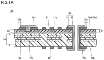
- Fig. 1A is a cross-sectional view of printed wiring board 100.
- Fig. 1B is a partially enlarged view of Fig. 1A .
- printed wiring board 100 includes a base material 10, a conductive pattern 21 and a conductive pattern 22, and a plating layer 30.
- Base material 10 has a main surface 10a and a main surface 10b.
- Main surface 10a and main surface 10b are end faces of base material 10 in the thickness direction.
- Main surface 10b is the opposite surface to main surface 10a.
- a through hole 10c is formed in base material 10. Through hole 10c extends through base material 10 along the thickness direction.
- Base material 10 includes a dielectric layer 11 and a substrate 12.
- Dielectric layer 11 is disposed above substrate 12 to cover a conductive pattern 12a described below.
- Dielectric layer 11 and substrate 12 are respectively located closer to main surface 10a and main surface 10b of base material 10.
- Substrate 12 is, for example, a rigid substrate.
- Substrate 12 may be, however, a flexible substrate.
- Dielectric layer 11 has a main surface 11a and a main surface 11b.
- Main surface 11a and main surface 11b are end faces of dielectric layer 11 in the thickness direction.
- Main surface 11a is included in main surface 10a.
- Main surface 11b is the opposite surface to main surface 11a and faces substrate 12.
- a hole 11c is formed in dielectric layer 11. Hole 11c extends through dielectric layer 11 along the thickness direction. Conductive pattern 12a described below is exposed from hole 11c.
- the thickness of dielectric layer 11 will be referred to as thickness T1.
- Thickness T1 is 50 ⁇ m or more and 500 ⁇ m or less.
- the aspect ratio of hole 11c is 0.5 or more and 2.0 or less. The aspect ratio of hole 11c is calculated by dividing thickness T1 by the maximum value of the opening width of hole 11c.
- Thickness T1 and the aspect ratio of hole 11c are measured by the following method.
- Thickness T1 is obtained by calculating the average value of the measured values at these ten points.
- the opening width of hole 11c is measured in the cross-sectional image described above.
- the aspect ratio of hole 11c is obtained by dividing thickness T1 obtained as described above by this measured value.
- Dielectric layer 11 is a layer formed by using a dielectric.
- Dielectric layer 11 includes, for example, fluororesin and filler that is mixed in the fluororesin.
- the fluororesin is, for example, polytetrafluoroethylene.
- the filler is formed by using, for example, silica.
- the silica may be a natural product or a synthetic product.
- the silica may be crystalline silica or amorphous silica.
- the silica may be formed by a dry process or a wet process. It is preferable from the perspectives of availability and quality that the silica be a synthetic product formed by a dry process.
- the mass ratio of the filler to the fluororesin is obtained by dividing the mass of the filler included in dielectric layer 11 per unit volume by the mass of the fluororesin included in dielectric layer 11 per unit volume.
- the mass ratio of the filler to the fluororesin is, for example, 1.3 or more. Setting the mass ratio of the filler to the fluororesin to 1.3 or more decreases the thermal expansion coefficient of dielectric layer 11 and improves the dimensional stability of dielectric layer 11. It is preferable that the mass ratio of the filler to the fluororesin be 1.5 or more. It is more preferable that the mass ratio of the filler to the fluororesin be 1.6 or more.
- the mass ratio of the filler to the fluororesin is, for example, 2.2 or less. Setting the mass ratio of the filler to the fluororesin to 2.2 or less makes it possible to suppress decreases in handleability and peel strength caused by the embrittlement of dielectric layer 11. It is preferable that the mass ratio of the filler to the fluororesin be 2.0 or less.
- the mass ratio of the filler to the fluororesin is measured by the following method. First, a cross-sectional image of dielectric layer 11 is acquired by using an SEM. Second, EDX (Energy Dispersive X-ray spectroscopy) analyses are done at any 30 points on the acquired cross-sectional image, thereby obtaining the mass ratios between the filler composition atoms and the fluorine atoms at the respective points.
- EDX Electronic Dispersive X-ray spectroscopy
- the mass ratio of the filler to the fluororesin is obtained by calculating the mass ratios between the filler and the fluororesin at the respective points based on the mass ratios between the filler composition atoms and the fluorine atoms and averaging the calculated mass ratios between the filler and the fluororesin with respect to the 30 points.
- the average particle diameter of the filler is, for example, 0.3 ⁇ m or more. It is preferable that the average particle diameter of the filler be 0.5 ⁇ m or more. It is more preferable that the average particle diameter of the filler be 1.0 ⁇ m or more. The average particle diameter of the filler is, for example, 4.0 ⁇ m or less. Setting the average particle diameter of the filler to 4.0 ⁇ m or less makes it possible to secure the uniformity of the thickness of dielectric layer 11. It is preferable that the average particle diameter of the filler be 3.0 ⁇ m or less. It is more preferable that the average particle diameter of the filler be 2.0 ⁇ m or less.
- the average particle diameter of the filler is the particle diameter of a primary particle and is represented by the median diameter D50 of the particle size distribution.
- the average particle diameter of the filler is measured by using a particle diameter distribution measurement device (e.g., MT3300II of MicrotracBEL Corporation). Some types of fillers different from each other in average particle diameter may be used in combination as long as the average particle diameters fall within the range described above. It is preferable that the filler have a spherical shape to facilitate through hole 10c to be formed.
- Dielectric layer 11 may further include fluororesin other than polytetrafluoroethylene.
- the amount of the fluororesin other than polytetrafluoroethylene contained in dielectric layer 11 is, for example, 10 wt% or less.
- the amount of the fluororesin other than polytetrafluoroethylene contained in dielectric layer 11 is preferably 5 wt% or less.
- the composition ratio (atomic ratio) of the silicon on the inner wall surface of hole 11c is preferably 20% or more and 80% or less. It is to be noted that the composition ratio (atomic ratio) of the silicon on the inner wall surface of hole 11c is the ratio of the silicon atoms to the entire atoms included in the inner wall surface of hole 11c.
- the mass ratio of the silicon on the inner wall surface of hole 11c is measured by removing plating layer 30 and then doing an EDX (Energy Dispersive X-ray) analysis on the inner wall surface of hole 11c.
- the filler may include filler formed by using a material other than silica in addition to the filler formed by using silica.
- a material other than silica include aluminum oxide, magnesium oxide, calcium oxide, talc, barium sulfate, boron nitride, zinc oxide, potassium titanate, glass, titanium oxide, mica, and the like.
- the content rate (the value obtained by dividing the mass of the filler formed by using silica by the sum of the mass of the filler formed by using silica and the mass of the filler formed by using the material other than silica, and multiplying 100) of the filler formed by using silica is, for example, 60 wt% or more. It is preferable that the content rate of the filler formed by using silica be 70 wt% or more. It is more preferable that the content rate of the filler formed by using silica be 80 wt% or more.
- the content rate of the filler formed by using silica is measured by the following method. First, a cross-sectional image of dielectric layer 11 is acquired by using an SEM. Second, EDX analyses are done on 50 fillers included in the acquired cross-sectional image to identify the composition of each of the fillers and the content rate of the filler formed by using silica is obtained based on the composition.
- a liquid crystal polymer or polyphenylene ether may be used for dielectric layer 11 instead of the fluororesin.
- An olefin-based material such as polystyrene or polypropylene may be used for dielectric layer 11 instead of the fluororesin.
- the relative dielectric constant of dielectric layer 11 is, for example, 2.0 or more and 4.0 or less.
- the relative dielectric constant of dielectric layer 11 is preferably 2.2 or more and 3.3 or less.
- the dielectric dissipation factor of dielectric layer 11 is, for example, 0.003 or less. It is preferable that the dielectric dissipation factor of dielectric layer 11 be 0.002 or less. It is more preferable that the dielectric dissipation factor of dielectric layer 11 be 0.0014 or less.
- the relative dielectric constant and the dielectric dissipation factor of dielectric layer 11 are measured under conditions of 25°C and 80 GHz on the basis of IPC TM-650 2.5.5.13 by using the split-cylinder resonator method.
- Substrate 12 has conductive pattern 12a and a conductive pattern 12b.
- Conductive pattern 12a is disposed on the main surface of substrate 12 closer to dielectric layer 11.
- Conductive pattern 12b is disposed inside substrate 12.
- Conductive pattern 12a and conductive pattern 12b are partially exposed from the inner wall surface of through hole 10c.
- Conductive pattern 21 and conductive pattern 22 are respectively disposed on main surface 10a and main surface 10b. Conductive pattern 21 and conductive pattern 22 are each formed by using, for example, copper. A high-frequency signal flows in conductive pattern 21.
- the thickness of conductive pattern 21 will be referred to as thickness T2. Thickness T2 is, for example, 5 ⁇ m or more and 20 ⁇ m or less.
- Thickness T2 is measured by the following method. First, a cross-sectional image of conductive pattern 21 is acquired by using an electron microscope in any cross section orthogonal to the direction in which conductive pattern 21 extends. Second, the thickness of conductive pattern 21 is measured at any ten points on the cross-sectional image described above. Thickness T2 is obtained by calculating the average value of the measured values at these ten points. Thickness T2 is, however, measured in a place other than the places around through hole 10c and hole 11c.
- width W1 and width W2 The width of the bottom surface of conductive pattern 21 and the width of the upper surface of conductive pattern 21 in a cross-sectional view orthogonal to the direction in which conductive pattern 21 extends will be respectively referred to as width W1 and width W2. It is preferable that the value obtained by dividing width W2 by width W1 be 0.7 or more and 1.0 or less. It is to be noted that, as the value obtained by dividing width W2 by width W1 is closer to 1.0, the shape of conductive pattern 21 is closer to a rectangle (the rectangularity of the cross-sectional shape is higher) in the cross-sectional view orthogonal to the direction in which conductive pattern 21 extends.
- Width W1 and width W2 are measured by the following method.
- Plating layer 30 is also disposed on the inner wall surface of through hole 10c. It is to be noted that plating layer 30 may also be disposed on the side surface of conductive pattern 21 continuous with the inner wall surface of through hole 10c, the upper surface of conductive pattern 21 around through hole 10c, the side surface of conductive pattern 22 continuous with the inner wall surface of through hole 10c, and the upper surface of conductive pattern 22 around through hole 10c. Conductive pattern 21 and conductive pattern 22 are electrically connected to each other by plating layer 30.
- Plating layer 30 is also disposed on the inner wall surface of hole 11c and conductive pattern 12a exposed from hole 11c. It is to be noted that plating layer 30 may also be disposed on the side surface of conductive pattern 21 continuous with the inner wall surface of hole 11c and the upper surface of conductive pattern 21 around hole 11c. Conductive pattern 21 is electrically connected to conductive pattern 12a by plating layer 30.
- Plating layer 30 includes, for example, an electroless plating layer 31 and an electrolytic plating layer 32 disposed on electroless plating layer 31.
- Electroless plating layer 31 is a layer formed by electroless plating and electrolytic plating layer 32 is a layer formed by electrolytic plating.
- Electroless plating layer 31 is an underlying conductive layer for forming electrolytic plating layer 32.
- Plating layer 30 (electroless plating layer 31 and electrolytic plating layer 32) is formed by using, for example, copper. It is to be noted that a sputtering layer (a layer formed by sputtering) or a conductive particulate layer (a layer including a conductive particle) may be formed as the underlying conductive layer instead of electroless plating layer 31.
- the thickness of plating layer 30 disposed on conductive pattern 12a exposed from hole 11c will be referred to as thickness T3.
- Thickness T3 is measured by the following method. First, a cross-sectional image of plating layer 30 disposed on conductive pattern 12a exposed from hole 11c is acquired by using an SEM in any cross section parallel with the thickness direction of dielectric layer 11. Second, the minimum value of the thickness of plating layer 30 is measured by using the cross-sectional image described above.
- Thickness T3 is greater than thickness T2. That is, the value obtained by dividing thickness T3 by thickness T2 is greater than 1.0. If this is expressed from another perspective, electrolytic plating layer 32 is not disposed on conductive pattern 21 and conductive pattern 22 except for the region around through hole 10c and the region around hole 11c. Thickness T3 is, for example, 10 ⁇ m or more. Steps are formed between electroless plating layer 31 and electrolytic plating layer 32 around through hole 10c and hole 11c. Distance DIS between electroless plating layer 31 and electrolytic plating layer 32 on the front surface of electroless plating layer 31 exposed by this step may be 10 ⁇ m or more, or 10 ⁇ m or more and 20 ⁇ m or less.
- the following describes a method of manufacturing printed wiring board 100.
- Fig. 2 is a process chart of manufacturing printed wiring board 100.
- the method of manufacturing printed wiring board 100 includes preparation step S1, hole making step S2, first plating step S3, first resist pattern forming step S4, second plating step S5, first resist pattern removing step S6, second resist pattern forming step S7, etching step S8, and second resist pattern removing step S9.
- Hole making step S2 is performed after preparation step S1.
- First plating step S3 is performed after hole making step S2.
- First resist pattern forming step S4 is performed after first plating step S3.
- Second plating step S5 is performed after first resist pattern forming step S4.
- First resist pattern removing step S6 is performed after second plating step S5.
- Second resist pattern forming step S7 is performed after first resist pattern removing step S6.
- Etching step S8 is performed after second resist pattern forming step S7.
- Second resist pattern removing step S9 is performed after etching step S8.
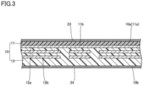
- Fig. 3 is a cross-sectional view describing preparation step S1.
- base material 10 is prepared in preparation step S1.
- copper foil 23 and copper foil 24 are respectively disposed on main surface 10a and main surface 10b of base material 10 prepared in preparation step S1.
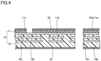
- Fig. 4 is a cross-sectional view describing hole making step S2. As illustrated in Fig. 4 , through hole 10c is formed in base material 10 and hole 11c is formed in dielectric layer 11 in hole making step S2. Through hole 10c and hole 11c are formed, for example, by drilling.
- Fig. 5 is a cross-sectional view describing first plating step S3.
- electroless plating layer 31 is formed on copper foil 23 and copper foil 24 in first plating step S3.
- Electroless plating layer 31 is also formed on the inner wall surface of through hole 10c, the side surface of copper foil 23 continuous with the inner wall surface of through hole 10c, the side surface of copper foil 24 continuous with the inner wall surface of through hole 10c, the inner wall surface of hole 11c, the side surface of copper foil 23 continuous with the inner wall surface of hole 11c, the side surface of copper foil 24 continuous with the inner wall surface of hole 11c, and conductive pattern 12a exposed from hole 11c.
- Fig. 6 is a cross-sectional view describing first resist pattern forming step S4.
- a resist pattern 41 and a resist pattern 42 are respectively formed above copper foil 23 and copper foil 24 with electroless plating layer 31 interposed in between in first resist pattern forming step S4.
- Resist pattern 41 has an opening 41a and an opening 41b. Opening 41a is located around through hole 10c. Opening 41b is located around hole 11c.
- Resist pattern 42 has an opening 42a. Opening 42a is located around through hole 10c.
- first resist pattern forming step S4 dry film resists are bonded onto copper foil 23 and copper foil 24. Second, exposure and development partially remove the dry film resists to make opening 41a, opening 41b, and opening 42a. In addition, the portion of the dry film resist on which opening 41a and opening 41b are not formed serves as resist pattern 41 and the portion of the dry film resist on which opening 42a is not formed serves as resist pattern 42.
- Fig. 7 is a cross-sectional view describing second plating step S5.
- electrolytic plating layer 32 is formed on electroless plating layer 31 in second plating step S5.
- electrolytic plating is performed by energizing electroless plating layer 31 to form electrolytic plating layer 32 on electroless plating layer 31. That is, button plating is performed in second plating step S5.
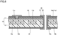
- Fig. 8 is a cross-sectional view describing first resist pattern removing step S6. As illustrated in Fig. 8 , resist pattern 41 is removed from copper foil 23 and resist pattern 42 is removed from copper foil 24 in first resist pattern removing step S6.
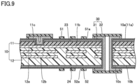
- Fig. 9 is a cross-sectional view describing second resist pattern forming step S7.
- a resist pattern 51 and a resist pattern 52 are respectively formed above copper foil 23 and copper foil 24 with electroless plating layer 31 interposed in between in second resist pattern forming step S7.
- Resist pattern 51 has an opening 51a and resist pattern 52 has an opening 52a.
- Copper foil 23 and electroless plating layer 31 thereon are exposed from opening 51a and copper foil 24 and electroless plating layer 31 thereon are exposed from opening 52a.
- resist pattern 51 and resist pattern 52 are formed by bonding dry film resists onto copper foil 23 and copper foil 24, and exposing and developing the dry films.
- Fig. 10 is a cross-sectional view describing etching step S8.
- Copper foil 23 and copper foil 24 are etched by using resist pattern 51 and resist pattern 52 as masks in etching step S8. This removes copper foil 23 and the portion of electroless plating layer 31 exposed from opening 51a and copper foil 24 and the portion of electroless plating layer 31 exposed from opening 52a to form conductive pattern 21 and conductive pattern 22.
- Resist pattern 51 is removed from conductive pattern 21 and resist pattern 52 is removed from conductive pattern 22 in second resist pattern removing step S9.
- Printed wiring board 100 having the structure illustrated in each of Figs. 1A and 1B is thus manufactured.
- electrolytic plating layer 32 is formed on the whole of electroless plating layer 31 in second plating step S5.
- electrolytic plating layer 32 is formed on the whole of electroless plating layer 31 in second plating step S5.
- electrolytic plating layer 32 has to be etched in etching step S8 in addition to copper foil 23, copper foil 24, and electroless plating layer 31.
- thick plating layer 30 when thickness T1 is 50 ⁇ m or more and the aspect ratio of hole 11c is 0.5 or more to secure the transmission characteristics of conductive pattern 21 in which a high-frequency signal flows, it is difficult to form plating layer 30 on conductive pattern 12a exposed from hole 11c. To secure reliability, it is thus preferable to form thick plating layer 30. However, the formation of thick plating layer 30 further increases the time necessary for etching step S8 and further decreases the transmission characteristics of conductive pattern 21 in which a high-frequency signal flows.
- First resist pattern forming step S4 is performed in printed wiring board 100 and it is thus sufficient if only copper foil 23, copper foil 24, and electroless plating layer 31 are etched in etching step S8. As a result, it takes a shorter time to perform etching step S8, and the width (cross-sectional area) of conductive pattern 21 varies less and the rectangularity of conductive pattern 21 increases. In this way, according to printed wiring board 100, the transmission characteristics of conductive pattern 21 in which a high-frequency signal flows are improved.
- the adhesiveness between plating layer 30 and the inner wall surface of hole 11c decreases and thick plating layer 30 is thus formed to improve reliability.
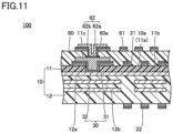
- Fig. 11 is a cross-sectional view of printed wiring board 100 according to a modification example. As illustrated in Fig. 11 , it is preferable that the filling ratio of hole 11c with plating layer 30 be 100%.
- Fig. 12 is a cross-sectional view for describing the filling ratio of hole 11c with plating layer 30. As illustrated in Fig. 12 , the distance between the upper surface of plating layer 30 and the upper surface of conductive pattern 12a around hole 11c will be referred to as distance DIS1. The minimum value of the distance between the upper surface of plating layer 30 disposed on conductive pattern 12a exposed from hole 11c and the upper surface of conductive pattern 12a will be referred to as distance DIS2. Distance DIS2 is divided by distance DIS1 and then multiplied by 100 to calculate the filling ratio of hole 11c with plating layer 30.
- a dielectric layer 60 may be disposed on dielectric layer 11 to cover plating layer 30 and conductive pattern 21.
- a conductive pattern 61 may be disposed on dielectric layer 60.
- a hole 60a from which plating layer 30 that fills hole 11c is exposed is formed in dielectric layer 60.
- Conductive pattern 61 is electrically connected to plating layer 30 by a plating layer 62 disposed on the inner wall surface of hole 60a, plating layer 30 exposed from hole 60a, the side surface of conductive pattern 61 continuous with the inner wall surface of hole 60a, and the upper surface of conductive pattern 61 around hole 60a.
- plating layer 62 includes an electroless plating layer 62a and an electrolytic plating layer 62b disposed on electroless plating layer 62a as with plating layer 30.
- the filling ratio is 100%, that is, when the upper surface of plating layer 30 disposed on conductive pattern 12a exposed from hole 11c has no dent, it is possible to stack still another dielectric layer on dielectric layer 11 and further build up a conductive pattern.
- the filling ratio is 100%, it is possible to mount a part on plating layer 30 that fills hole 11c.
Landscapes
- Engineering & Computer Science (AREA)
- Microelectronics & Electronic Packaging (AREA)
- Manufacturing & Machinery (AREA)
- Printing Elements For Providing Electric Connections Between Printed Circuits (AREA)
- Structure Of Printed Boards (AREA)
- Parts Printed On Printed Circuit Boards (AREA)
Abstract
Description
- The present disclosure relates to a printed wiring board. This application claims priority based on
Japanese Patent Application No. 2022-000261 filed on January 4, 2022 - For example,
Japanese Patent Laying-Open No. 2004-087550 PTL 1, first, a base material is prepared. The base material has a first main surface and a second main surface, and copper foil is disposed on the first main surface and the second main surface. Second, a hole is formed in the base material. A first conductive pattern disposed in the base material is exposed from the hole. - Third, a plating layer is formed on the copper foil, an inner wall surface of the hole, and the first conductive pattern. Fourth, the copper foil and the plating layer on the copper foil are patterned by etching that uses a resist pattern as a mask, thereby serving as a second conductive pattern.
- PTL 1:
Japanese Patent Laying-Open No. 2004-087550 - A printed wiring board according to the present disclosure includes: a first conductive pattern; a dielectric layer that is disposed to cover the first conductive pattern; a second conductive pattern that is disposed on the dielectric layer; and a plating layer. A thickness of the dielectric layer is 50 µm or more and 500 µm or less. A hole from which the first conductive pattern is exposed is formed in the dielectric layer. An aspect ratio of the hole is 0.5 or more and 2.0 or less. The plating layer is disposed on at least an inner wall surface of the hole and the first conductive pattern exposed from the hole, and electrically connected to the second conductive pattern. A thickness of the plating layer disposed on the first conductive pattern exposed from the hole is greater than a thickness of the second conductive pattern.
-
-
Fig. 1A is a cross-sectional view of a printedwiring board 100. -
Fig. 1B is a partially enlarged view ofFig. 1A . -
Fig. 2 is a process chart of manufacturing printedwiring board 100. -
Fig. 3 is a cross-sectional view describing preparation step S1. -
Fig. 4 is a cross-sectional view describing hole making step S2. -
Fig. 5 is a cross-sectional view describing first plating step S3. -
Fig. 6 is a cross-sectional view describing first resist pattern forming step S4. -
Fig. 7 is a cross-sectional view describing second plating step S5. -
Fig. 8 is a cross-sectional view describing first resist pattern removing step S6. -
Fig. 9 is a cross-sectional view describing second resist pattern forming step S7. -
Fig. 10 is a cross-sectional view describing etching step S8. -
Fig. 11 is a cross-sectional view of printedwiring board 100 according to a modification example. -
Fig. 12 is a cross-sectional view for describing a filling ratio of ahole 11c with aplating layer 30. - A printed wiring board described in
PTL 1 has a long etching time because it is necessary to etch copper foil and a plating layer on the copper foil when a second conductive pattern is formed. As the etching time is longer, the cross-sectional rectangularity of the second conductive pattern decreases and the width (cross-sectional area) of the second conductive pattern varies from place to place. The decreased cross-sectional rectangularity of the second conductive pattern and the more varying width (cross-sectional area) of the second conductive pattern decrease the transmission characteristics with respect to a high-frequency signal flowing in the second conductive pattern. - The present disclosure has been devised in view of the problem of the conventional technology as described above. More specifically, the present disclosure provides a printed wiring board that makes it possible to improve the transmission characteristics with respect to a high-frequency signal flowing in the conductive pattern.
- The printed wiring board according to the present disclosure makes it possible to improve the transmission characteristics with respect to a high-frequency signal flowing in the conductive pattern.
- First, an embodiment of the present disclosure will be listed and described.
- (1) A printed wiring board according to the embodiment includes a first conductive pattern, a dielectric layer that is disposed to cover the first conductive pattern, a second conductive pattern that is disposed on the dielectric layer, and a plating layer. A thickness of the dielectric layer is 50 µm or more and 500 µm or less. A hole from which the first conductive pattern is exposed is formed in the dielectric layer. An aspect ratio of the hole is 0.5 or more and 2.0 or less. The plating layer is disposed on at least an inner wall surface of the hole and the first conductive pattern exposed from the hole, and electrically connected to the second conductive pattern. A thickness of the plating layer disposed on the first conductive pattern exposed from the hole is greater than a thickness of the second conductive pattern.
The printed wiring board according to (1) described above makes it possible to improve the transmission characteristics with respect to a high-frequency signal flowing in the conductive pattern. - (2) In the printed wiring board according to (1), the dielectric layer may include fluororesin and filler that is mixed in the fluororesin. The filler may be formed by using silica.
- (3) In the printed wiring board according to (2), a composition ratio of silicon on the inner wall surface of the hole may be 20% or more and 80% or less.
The printed wiring board according to (3) makes it possible to improve the transmission characteristics with respect to a high-frequency signal flowing in the conductive pattern even when there is no choice but to form a thick plating layer on the inner wall surface of a through hole. - (4) In the printed wiring board according to (1) to (3), the plating layer may include an underlying conductive layer and an electrolytic plating layer that is disposed on the underlying conductive layer. A step may be formed between the underlying conductive layer and the electrolytic plating layer around the hole.
- (5) In the printed wiring board according to (4), a distance between an end of the underlying conductive layer and the electrolytic plating layer on a front surface of the underlying conductive layer exposed by the step may be 10 µm or more.
- With reference to the drawings, details of the embodiment of the present disclosure will be described. In the following drawings, the same or corresponding portions will be denoted by the same reference numerals and duplicate description will not be repeated. The printed wiring board according to the embodiment will be referred to as a printed
wiring board 100. - The following describes a configuration of printed
wiring board 100. -
Fig. 1A is a cross-sectional view of printedwiring board 100.Fig. 1B is a partially enlarged view ofFig. 1A . As illustrated inFigs. 1A and1B , printedwiring board 100 includes abase material 10, aconductive pattern 21 and aconductive pattern 22, and aplating layer 30. -
Base material 10 has amain surface 10a and amain surface 10b.Main surface 10a andmain surface 10b are end faces ofbase material 10 in the thickness direction.Main surface 10b is the opposite surface tomain surface 10a. A throughhole 10c is formed inbase material 10. Throughhole 10c extends throughbase material 10 along the thickness direction. -
Base material 10 includes adielectric layer 11 and asubstrate 12.Dielectric layer 11 is disposed abovesubstrate 12 to cover aconductive pattern 12a described below.Dielectric layer 11 andsubstrate 12 are respectively located closer tomain surface 10a andmain surface 10b ofbase material 10.Substrate 12 is, for example, a rigid substrate.Substrate 12 may be, however, a flexible substrate. -
Dielectric layer 11 has amain surface 11a and amain surface 11b.Main surface 11a andmain surface 11b are end faces ofdielectric layer 11 in the thickness direction.Main surface 11a is included inmain surface 10a.Main surface 11b is the opposite surface tomain surface 11a and facessubstrate 12. Ahole 11c is formed indielectric layer 11.Hole 11c extends throughdielectric layer 11 along the thickness direction.Conductive pattern 12a described below is exposed fromhole 11c. - The thickness of
dielectric layer 11 will be referred to as thickness T1. Thickness T1 is 50 µm or more and 500 µm or less. The aspect ratio ofhole 11c is 0.5 or more and 2.0 or less. The aspect ratio ofhole 11c is calculated by dividing thickness T1 by the maximum value of the opening width ofhole 11c. - Thickness T1 and the aspect ratio of
hole 11c are measured by the following method. First, a cross-sectional image is acquired by using an electron microscope (SEM: Scanning Electron Microscope) in a cross section parallel with the thickness direction ofdielectric layer 11 in which the opening width ofhole 11c is maximized. Second, the thickness ofdielectric layer 11 is measured at any ten points on the cross-sectional image described above. Thickness T1 is obtained by calculating the average value of the measured values at these ten points. - Third, the opening width of
hole 11c is measured in the cross-sectional image described above. The aspect ratio ofhole 11c is obtained by dividing thickness T1 obtained as described above by this measured value. -
Dielectric layer 11 is a layer formed by using a dielectric.Dielectric layer 11 includes, for example, fluororesin and filler that is mixed in the fluororesin. The fluororesin is, for example, polytetrafluoroethylene. The filler is formed by using, for example, silica. - The silica may be a natural product or a synthetic product. The silica may be crystalline silica or amorphous silica. In the case of a synthetic product, the silica may be formed by a dry process or a wet process. It is preferable from the perspectives of availability and quality that the silica be a synthetic product formed by a dry process.
- The mass ratio of the filler to the fluororesin is obtained by dividing the mass of the filler included in
dielectric layer 11 per unit volume by the mass of the fluororesin included indielectric layer 11 per unit volume. - The mass ratio of the filler to the fluororesin is, for example, 1.3 or more. Setting the mass ratio of the filler to the fluororesin to 1.3 or more decreases the thermal expansion coefficient of
dielectric layer 11 and improves the dimensional stability ofdielectric layer 11. It is preferable that the mass ratio of the filler to the fluororesin be 1.5 or more. It is more preferable that the mass ratio of the filler to the fluororesin be 1.6 or more. - The mass ratio of the filler to the fluororesin is, for example, 2.2 or less. Setting the mass ratio of the filler to the fluororesin to 2.2 or less makes it possible to suppress decreases in handleability and peel strength caused by the embrittlement of
dielectric layer 11. It is preferable that the mass ratio of the filler to the fluororesin be 2.0 or less. - The mass ratio of the filler to the fluororesin is measured by the following method. First, a cross-sectional image of
dielectric layer 11 is acquired by using an SEM. Second, EDX (Energy Dispersive X-ray spectroscopy) analyses are done at any 30 points on the acquired cross-sectional image, thereby obtaining the mass ratios between the filler composition atoms and the fluorine atoms at the respective points. Third, the mass ratio of the filler to the fluororesin is obtained by calculating the mass ratios between the filler and the fluororesin at the respective points based on the mass ratios between the filler composition atoms and the fluorine atoms and averaging the calculated mass ratios between the filler and the fluororesin with respect to the 30 points. - The average particle diameter of the filler is, for example, 0.3 µm or more. It is preferable that the average particle diameter of the filler be 0.5 µm or more. It is more preferable that the average particle diameter of the filler be 1.0 µm or more. The average particle diameter of the filler is, for example, 4.0 µm or less. Setting the average particle diameter of the filler to 4.0 µm or less makes it possible to secure the uniformity of the thickness of
dielectric layer 11. It is preferable that the average particle diameter of the filler be 3.0 µm or less. It is more preferable that the average particle diameter of the filler be 2.0 µm or less. The average particle diameter of the filler is the particle diameter of a primary particle and is represented by the median diameter D50 of the particle size distribution. The average particle diameter of the filler is measured by using a particle diameter distribution measurement device (e.g., MT3300II of MicrotracBEL Corporation). Some types of fillers different from each other in average particle diameter may be used in combination as long as the average particle diameters fall within the range described above. It is preferable that the filler have a spherical shape to facilitate throughhole 10c to be formed. -
Dielectric layer 11 may further include fluororesin other than polytetrafluoroethylene. The amount of the fluororesin other than polytetrafluoroethylene contained indielectric layer 11 is, for example, 10 wt% or less. The amount of the fluororesin other than polytetrafluoroethylene contained indielectric layer 11 is preferably 5 wt% or less. - The composition ratio (atomic ratio) of the silicon on the inner wall surface of
hole 11c is preferably 20% or more and 80% or less. It is to be noted that the composition ratio (atomic ratio) of the silicon on the inner wall surface ofhole 11c is the ratio of the silicon atoms to the entire atoms included in the inner wall surface ofhole 11c. The mass ratio of the silicon on the inner wall surface ofhole 11c is measured by removingplating layer 30 and then doing an EDX (Energy Dispersive X-ray) analysis on the inner wall surface ofhole 11c. - The filler may include filler formed by using a material other than silica in addition to the filler formed by using silica. Specific examples of the material other than silica include aluminum oxide, magnesium oxide, calcium oxide, talc, barium sulfate, boron nitride, zinc oxide, potassium titanate, glass, titanium oxide, mica, and the like.
- The content rate (the value obtained by dividing the mass of the filler formed by using silica by the sum of the mass of the filler formed by using silica and the mass of the filler formed by using the material other than silica, and multiplying 100) of the filler formed by using silica is, for example, 60 wt% or more. It is preferable that the content rate of the filler formed by using silica be 70 wt% or more. It is more preferable that the content rate of the filler formed by using silica be 80 wt% or more.
- The content rate of the filler formed by using silica is measured by the following method. First, a cross-sectional image of
dielectric layer 11 is acquired by using an SEM. Second, EDX analyses are done on 50 fillers included in the acquired cross-sectional image to identify the composition of each of the fillers and the content rate of the filler formed by using silica is obtained based on the composition. - A liquid crystal polymer or polyphenylene ether may be used for
dielectric layer 11 instead of the fluororesin. An olefin-based material such as polystyrene or polypropylene may be used fordielectric layer 11 instead of the fluororesin. - The relative dielectric constant of
dielectric layer 11 is, for example, 2.0 or more and 4.0 or less. The relative dielectric constant ofdielectric layer 11 is preferably 2.2 or more and 3.3 or less. The dielectric dissipation factor ofdielectric layer 11 is, for example, 0.003 or less. It is preferable that the dielectric dissipation factor ofdielectric layer 11 be 0.002 or less. It is more preferable that the dielectric dissipation factor ofdielectric layer 11 be 0.0014 or less. The relative dielectric constant and the dielectric dissipation factor ofdielectric layer 11 are measured under conditions of 25°C and 80 GHz on the basis of IPC TM-650 2.5.5.13 by using the split-cylinder resonator method. -
Substrate 12 hasconductive pattern 12a and aconductive pattern 12b.Conductive pattern 12a is disposed on the main surface ofsubstrate 12 closer todielectric layer 11.Conductive pattern 12b is disposed insidesubstrate 12.Conductive pattern 12a andconductive pattern 12b are partially exposed from the inner wall surface of throughhole 10c. -
Conductive pattern 21 andconductive pattern 22 are respectively disposed onmain surface 10a andmain surface 10b.Conductive pattern 21 andconductive pattern 22 are each formed by using, for example, copper. A high-frequency signal flows inconductive pattern 21. The thickness ofconductive pattern 21 will be referred to as thickness T2. Thickness T2 is, for example, 5 µm or more and 20 µm or less. - Thickness T2 is measured by the following method. First, a cross-sectional image of
conductive pattern 21 is acquired by using an electron microscope in any cross section orthogonal to the direction in whichconductive pattern 21 extends. Second, the thickness ofconductive pattern 21 is measured at any ten points on the cross-sectional image described above. Thickness T2 is obtained by calculating the average value of the measured values at these ten points. Thickness T2 is, however, measured in a place other than the places around throughhole 10c andhole 11c. - The width of the bottom surface of
conductive pattern 21 and the width of the upper surface ofconductive pattern 21 in a cross-sectional view orthogonal to the direction in whichconductive pattern 21 extends will be respectively referred to as width W1 and width W2. It is preferable that the value obtained by dividing width W2 by width W1 be 0.7 or more and 1.0 or less. It is to be noted that, as the value obtained by dividing width W2 by width W1 is closer to 1.0, the shape ofconductive pattern 21 is closer to a rectangle (the rectangularity of the cross-sectional shape is higher) in the cross-sectional view orthogonal to the direction in whichconductive pattern 21 extends. - Width W1 and width W2 are measured by the following method. First, cross-sectional images of
conductive pattern 21 are acquired by using an SEM in any ten cross sections orthogonal to the direction in whichconductive pattern 21 extends. Second, the width of the bottom surface ofconductive pattern 21 and the width of the upper surface ofconductive pattern 21 are measured in each of the cross-sectional images described above. Width W1 and width W2 are obtained by averaging these measured values with respect to the ten cross-sectional images. - Plating
layer 30 is also disposed on the inner wall surface of throughhole 10c. It is to be noted that platinglayer 30 may also be disposed on the side surface ofconductive pattern 21 continuous with the inner wall surface of throughhole 10c, the upper surface ofconductive pattern 21 around throughhole 10c, the side surface ofconductive pattern 22 continuous with the inner wall surface of throughhole 10c, and the upper surface ofconductive pattern 22 around throughhole 10c.Conductive pattern 21 andconductive pattern 22 are electrically connected to each other by platinglayer 30. - Plating
layer 30 is also disposed on the inner wall surface ofhole 11c andconductive pattern 12a exposed fromhole 11c. It is to be noted that platinglayer 30 may also be disposed on the side surface ofconductive pattern 21 continuous with the inner wall surface ofhole 11c and the upper surface ofconductive pattern 21 aroundhole 11c.Conductive pattern 21 is electrically connected toconductive pattern 12a by platinglayer 30. - Plating
layer 30 includes, for example, anelectroless plating layer 31 and anelectrolytic plating layer 32 disposed onelectroless plating layer 31.Electroless plating layer 31 is a layer formed by electroless plating andelectrolytic plating layer 32 is a layer formed by electrolytic plating.Electroless plating layer 31 is an underlying conductive layer for formingelectrolytic plating layer 32. Plating layer 30 (electroless plating layer 31 and electrolytic plating layer 32) is formed by using, for example, copper. It is to be noted that a sputtering layer (a layer formed by sputtering) or a conductive particulate layer (a layer including a conductive particle) may be formed as the underlying conductive layer instead ofelectroless plating layer 31. - The thickness of plating
layer 30 disposed onconductive pattern 12a exposed fromhole 11c will be referred to as thickness T3. Thickness T3 is measured by the following method. First, a cross-sectional image of platinglayer 30 disposed onconductive pattern 12a exposed fromhole 11c is acquired by using an SEM in any cross section parallel with the thickness direction ofdielectric layer 11. Second, the minimum value of the thickness of platinglayer 30 is measured by using the cross-sectional image described above. - Thickness T3 is greater than thickness T2. That is, the value obtained by dividing thickness T3 by thickness T2 is greater than 1.0. If this is expressed from another perspective,
electrolytic plating layer 32 is not disposed onconductive pattern 21 andconductive pattern 22 except for the region around throughhole 10c and the region aroundhole 11c. Thickness T3 is, for example, 10 µm or more. Steps are formed betweenelectroless plating layer 31 andelectrolytic plating layer 32 around throughhole 10c andhole 11c. Distance DIS betweenelectroless plating layer 31 andelectrolytic plating layer 32 on the front surface ofelectroless plating layer 31 exposed by this step may be 10 µm or more, or 10 µm or more and 20 µm or less. - The following describes a method of manufacturing printed
wiring board 100. -
Fig. 2 is a process chart of manufacturing printedwiring board 100. As illustrated inFig. 2 , the method of manufacturing printedwiring board 100 includes preparation step S1, hole making step S2, first plating step S3, first resist pattern forming step S4, second plating step S5, first resist pattern removing step S6, second resist pattern forming step S7, etching step S8, and second resist pattern removing step S9. - Hole making step S2 is performed after preparation step S1. First plating step S3 is performed after hole making step S2. First resist pattern forming step S4 is performed after first plating step S3. Second plating step S5 is performed after first resist pattern forming step S4. First resist pattern removing step S6 is performed after second plating step S5. Second resist pattern forming step S7 is performed after first resist pattern removing step S6. Etching step S8 is performed after second resist pattern forming step S7. Second resist pattern removing step S9 is performed after etching step S8.
-
Fig. 3 is a cross-sectional view describing preparation step S1. As illustrated inFig. 3 ,base material 10 is prepared in preparation step S1. It is to be noted thatcopper foil 23 andcopper foil 24 are respectively disposed onmain surface 10a andmain surface 10b ofbase material 10 prepared in preparation step S1. -
Fig. 4 is a cross-sectional view describing hole making step S2. As illustrated inFig. 4 , throughhole 10c is formed inbase material 10 andhole 11c is formed indielectric layer 11 in hole making step S2. Throughhole 10c andhole 11c are formed, for example, by drilling. -
Fig. 5 is a cross-sectional view describing first plating step S3. As illustrated inFig. 5 ,electroless plating layer 31 is formed oncopper foil 23 andcopper foil 24 in first plating step S3.Electroless plating layer 31 is also formed on the inner wall surface of throughhole 10c, the side surface ofcopper foil 23 continuous with the inner wall surface of throughhole 10c, the side surface ofcopper foil 24 continuous with the inner wall surface of throughhole 10c, the inner wall surface ofhole 11c, the side surface ofcopper foil 23 continuous with the inner wall surface ofhole 11c, the side surface ofcopper foil 24 continuous with the inner wall surface ofhole 11c, andconductive pattern 12a exposed fromhole 11c. -
Fig. 6 is a cross-sectional view describing first resist pattern forming step S4. As illustrated inFig. 6 , a resistpattern 41 and a resistpattern 42 are respectively formed abovecopper foil 23 andcopper foil 24 withelectroless plating layer 31 interposed in between in first resist pattern forming step S4. Resistpattern 41 has anopening 41a and anopening 41b.Opening 41a is located around throughhole 10c.Opening 41b is located aroundhole 11c. Resistpattern 42 has anopening 42a.Opening 42a is located around throughhole 10c. - In first resist pattern forming step S4, first, dry film resists are bonded onto
copper foil 23 andcopper foil 24. Second, exposure and development partially remove the dry film resists to makeopening 41a, opening 41b, andopening 42a. In addition, the portion of the dry film resist on whichopening 41a andopening 41b are not formed serves as resistpattern 41 and the portion of the dry film resist on whichopening 42a is not formed serves as resistpattern 42. -
Fig. 7 is a cross-sectional view describing second plating step S5. As illustrated inFig. 7 ,electrolytic plating layer 32 is formed onelectroless plating layer 31 in second plating step S5. In second plating step S5, electrolytic plating is performed by energizingelectroless plating layer 31 to formelectrolytic plating layer 32 onelectroless plating layer 31. That is, button plating is performed in second plating step S5. -
Fig. 8 is a cross-sectional view describing first resist pattern removing step S6. As illustrated inFig. 8 , resistpattern 41 is removed fromcopper foil 23 and resistpattern 42 is removed fromcopper foil 24 in first resist pattern removing step S6. -
Fig. 9 is a cross-sectional view describing second resist pattern forming step S7. As illustrated inFig. 9 , a resistpattern 51 and a resistpattern 52 are respectively formed abovecopper foil 23 andcopper foil 24 withelectroless plating layer 31 interposed in between in second resist pattern forming step S7. Resistpattern 51 has anopening 51a and resistpattern 52 has anopening 52a.Copper foil 23 andelectroless plating layer 31 thereon are exposed from opening 51a andcopper foil 24 andelectroless plating layer 31 thereon are exposed from opening 52a. It is to be noted that resistpattern 51 and resistpattern 52 are formed by bonding dry film resists ontocopper foil 23 andcopper foil 24, and exposing and developing the dry films. -
Fig. 10 is a cross-sectional view describing etching step S8.Copper foil 23 andcopper foil 24 are etched by using resistpattern 51 and resistpattern 52 as masks in etching step S8. This removescopper foil 23 and the portion ofelectroless plating layer 31 exposed from opening 51a andcopper foil 24 and the portion ofelectroless plating layer 31 exposed from opening 52a to formconductive pattern 21 andconductive pattern 22. - Resist
pattern 51 is removed fromconductive pattern 21 and resistpattern 52 is removed fromconductive pattern 22 in second resist pattern removing step S9. Printedwiring board 100 having the structure illustrated in each ofFigs. 1A and1B is thus manufactured. - The following describes an advantageous effect of printed
wiring board 100. - When first resist pattern forming step S4 is not performed,
electrolytic plating layer 32 is formed on the whole ofelectroless plating layer 31 in second plating step S5. In this case, to formconductive pattern 21 andconductive pattern 22, evenelectrolytic plating layer 32 has to be etched in etching step S8 in addition tocopper foil 23,copper foil 24, andelectroless plating layer 31. As a result, it takes a longer time to perform etching step S8, the width (cross-sectional area) ofconductive pattern 21 varies more and the rectangularity ofconductive pattern 21 decreases, and the transmission characteristics ofconductive pattern 21 in which a high-frequency signal flows decrease. - In particular, when thickness T1 is 50 µm or more and the aspect ratio of
hole 11c is 0.5 or more to secure the transmission characteristics ofconductive pattern 21 in which a high-frequency signal flows, it is difficult to form platinglayer 30 onconductive pattern 12a exposed fromhole 11c. To secure reliability, it is thus preferable to formthick plating layer 30. However, the formation ofthick plating layer 30 further increases the time necessary for etching step S8 and further decreases the transmission characteristics ofconductive pattern 21 in which a high-frequency signal flows. - First resist pattern forming step S4 is performed in printed
wiring board 100 and it is thus sufficient ifonly copper foil 23,copper foil 24, andelectroless plating layer 31 are etched in etching step S8. As a result, it takes a shorter time to perform etching step S8, and the width (cross-sectional area) ofconductive pattern 21 varies less and the rectangularity ofconductive pattern 21 increases. In this way, according to printedwiring board 100, the transmission characteristics ofconductive pattern 21 in which a high-frequency signal flows are improved. - For example, when much filler formed by using silica is exposed on the inner wall surface of
hole 11c in dielectric layer 11 (more specifically, the composition ratio of the silicon on the inner wall surface ofhole 11c indielectric layer 11 is 20% or more and 80% or less), the adhesiveness betweenplating layer 30 and the inner wall surface ofhole 11c decreases andthick plating layer 30 is thus formed to improve reliability. - It is sufficient in printed
wiring board 100 ifonly copper foil 23,copper foil 24, andelectroless plating layer 31 are etched in etching step S8. This suppresses an increase in the time necessary for etching step S8 even whenthick plating layer 30 is formed. Thus, according to printedwiring board 100, the transmission characteristics ofconductive pattern 21 in which a high-frequency signal flows are improved even whenthick plating layer 30 is formed. -
Fig. 11 is a cross-sectional view of printedwiring board 100 according to a modification example. As illustrated inFig. 11 , it is preferable that the filling ratio ofhole 11c with platinglayer 30 be 100%.Fig. 12 is a cross-sectional view for describing the filling ratio ofhole 11c with platinglayer 30. As illustrated inFig. 12 , the distance between the upper surface of platinglayer 30 and the upper surface ofconductive pattern 12a aroundhole 11c will be referred to as distance DIS1. The minimum value of the distance between the upper surface of platinglayer 30 disposed onconductive pattern 12a exposed fromhole 11c and the upper surface ofconductive pattern 12a will be referred to as distance DIS2. Distance DIS2 is divided by distance DIS1 and then multiplied by 100 to calculate the filling ratio ofhole 11c with platinglayer 30. - As illustrated in
Fig. 11 , adielectric layer 60 may be disposed ondielectric layer 11 to coverplating layer 30 andconductive pattern 21. Aconductive pattern 61 may be disposed ondielectric layer 60. Ahole 60a from whichplating layer 30 that fillshole 11c is exposed is formed indielectric layer 60.Conductive pattern 61 is electrically connected to platinglayer 30 by aplating layer 62 disposed on the inner wall surface ofhole 60a, platinglayer 30 exposed fromhole 60a, the side surface ofconductive pattern 61 continuous with the inner wall surface ofhole 60a, and the upper surface ofconductive pattern 61 aroundhole 60a. It is to be noted that platinglayer 62 includes anelectroless plating layer 62a and anelectrolytic plating layer 62b disposed onelectroless plating layer 62a as with platinglayer 30. - In this way, when the filling ratio is 100%, that is, when the upper surface of plating
layer 30 disposed onconductive pattern 12a exposed fromhole 11c has no dent, it is possible to stack still another dielectric layer ondielectric layer 11 and further build up a conductive pattern. Although not illustrated, when the filling ratio is 100%, it is possible to mount a part on platinglayer 30 that fillshole 11c. - The embodiment disclosed herein should be understood as an example in all respects and should not be understood as being restrictive. The scope of the present invention is demonstrated by not the embodiment described above, but CLAIMS. The scope of the present invention is intended to embrace all the modifications within the meaning and range equivalent to CLAIMS.
- 10 Base material; 10a Main surface; 10b Main surface; 10c Through hole; 11 Dielectric layer; 11a Main surface; 11b Main surface; 11c Hole; 12 Substrate; 12a Conductive pattern; 12b Conductive pattern; 21 Conductive pattern; 22 Conductive pattern; 23 Copper foil; 24 Copper foil; 30 Plating layer; 31 Electroless plating layer; 32 Electrolytic plating layer; 41 Resist pattern; 41a, 41b Opening; 42 Resist pattern; 42a Opening; 51 Resist pattern; 51a Opening; 52 Resist pattern; 52a Opening; 60 Dielectric layer; 61 Conductive pattern; 62 Plating layer; 62a Electroless plating layer; 62b Electrolytic plating layer; 100 Printed wiring board; P Measurement position; S1 Preparation step; S2 Hole making step; S3 First plating step; S4 First resist pattern forming step; S5 Second plating step; S6 First resist pattern removing step; S7 Second resist pattern forming step; S8 Etching step; S9 Second resist pattern removing step; DIS Distance; DIS1 Distance; DIS2 Distance; T1, T2, T3 Thickness; W1 Width; W2 Width.
Claims (5)
- A printed wiring board comprising:a first conductive pattern;a dielectric layer that is disposed to cover the first conductive pattern;a second conductive pattern that is disposed on the dielectric layer; anda plating layer, whereina thickness of the dielectric layer is 50 µm or more and 500 µm or less,a hole from which the first conductive pattern is exposed is formed in the dielectric layer,an aspect ratio of the hole is 0.5 or more and 2.0 or less,the plating layer is disposed on at least an inner wall surface of the hole and the first conductive pattern exposed from the hole, and electrically connected to the second conductive pattern, anda thickness of the plating layer disposed on the first conductive pattern exposed from the hole is greater than a thickness of the second conductive pattern.
- The printed wiring board according to claim 1, whereinthe dielectric layer includes fluororesin and filler that is mixed in the fluororesin, andthe filler is formed by using silica.
- The printed wiring board according to claim 2, wherein a composition ratio of silicon on the inner wall surface of the hole is 20% or more and 80% or less.
- The printed wiring board according to any one of claims 1 to 3, whereinthe plating layer includes an underlying conductive layer and an electrolytic plating layer that is disposed on the underlying conductive layer, anda step is formed between the underlying conductive layer and the electrolytic plating layer around the hole.
- The printed wiring board according to claim 4, wherein a distance between an end of the underlying conductive layer and the electrolytic plating layer on a front surface of the underlying conductive layer exposed by the step is 10 µm or more.
Applications Claiming Priority (2)
| Application Number | Priority Date | Filing Date | Title |
|---|---|---|---|
| JP2022000261 | 2022-01-04 | ||
| PCT/JP2022/047157 WO2023132246A1 (en) | 2022-01-04 | 2022-12-21 | Printed wiring board |
Publications (2)
| Publication Number | Publication Date |
|---|---|
| EP4462965A1 true EP4462965A1 (en) | 2024-11-13 |
| EP4462965A4 EP4462965A4 (en) | 2025-04-23 |
Family
ID=87073533
Family Applications (1)
| Application Number | Title | Priority Date | Filing Date |
|---|---|---|---|
| EP22918830.5A Pending EP4462965A4 (en) | 2022-01-04 | 2022-12-21 | PRINTED CIRCUIT BOARD |
Country Status (5)
| Country | Link |
|---|---|
| US (1) | US20250063661A1 (en) |
| EP (1) | EP4462965A4 (en) |
| JP (1) | JPWO2023132246A1 (en) |
| CN (1) | CN118511660A (en) |
| WO (1) | WO2023132246A1 (en) |
Family Cites Families (9)
| Publication number | Priority date | Publication date | Assignee | Title |
|---|---|---|---|---|
| MY144503A (en) * | 1998-09-14 | 2011-09-30 | Ibiden Co Ltd | Printed circuit board and method for its production |
| JP2002026515A (en) * | 2000-07-07 | 2002-01-25 | Toshiba Corp | Printed wiring board and method of manufacturing the same |
| JP2003304067A (en) * | 2002-04-11 | 2003-10-24 | Cmk Corp | Multilayer printed wiring board and manufacturing method thereof |
| JP2004087550A (en) | 2002-08-23 | 2004-03-18 | Toppan Printing Co Ltd | Printed wiring board |
| JP2007266606A (en) * | 2006-03-28 | 2007-10-11 | Endicott Interconnect Technologies Inc | Fluoropolymer insulating composition for circuit board, and circuit board including same |
| JP6350062B2 (en) * | 2013-10-09 | 2018-07-04 | 日立化成株式会社 | Manufacturing method of multilayer wiring board |
| JP6601814B2 (en) * | 2014-05-21 | 2019-11-06 | 住友電工プリントサーキット株式会社 | Printed wiring board and printed wiring board manufacturing method |
| JP7114893B2 (en) | 2017-12-14 | 2022-08-09 | 株式会社三洋物産 | game machine |
| WO2020145133A1 (en) * | 2019-01-11 | 2020-07-16 | ダイキン工業株式会社 | Fluororesin composition, fluororesin sheet, multilayer body and substrate for circuits |
-
2022
- 2022-12-21 JP JP2023572420A patent/JPWO2023132246A1/ja active Pending
- 2022-12-21 CN CN202280087606.6A patent/CN118511660A/en active Pending
- 2022-12-21 WO PCT/JP2022/047157 patent/WO2023132246A1/en not_active Ceased
- 2022-12-21 US US18/725,200 patent/US20250063661A1/en active Pending
- 2022-12-21 EP EP22918830.5A patent/EP4462965A4/en active Pending
Also Published As
| Publication number | Publication date |
|---|---|
| WO2023132246A1 (en) | 2023-07-13 |
| CN118511660A (en) | 2024-08-16 |
| JPWO2023132246A1 (en) | 2023-07-13 |
| EP4462965A4 (en) | 2025-04-23 |
| US20250063661A1 (en) | 2025-02-20 |
Similar Documents
| Publication | Publication Date | Title |
|---|---|---|
| TW436970B (en) | Photodefined integral capacitor with self-aligned dielectric and electrodes and method therefor | |
| CN102046853B (en) | Copper foil roughening treatment method and printed wiring board copper foil obtained by the roughening treatment method | |
| US20200358161A1 (en) | Substrate integrated waveguide and method for manufacturing the same | |
| KR100827524B1 (en) | Manufacturing Method of Semiconductor Device | |
| US20110283535A1 (en) | Wiring board and method of manufacturing the same | |
| US20150200164A1 (en) | Semiconductor Devices and Methods of Manufacture Thereof | |
| EP1145317A1 (en) | Coaxial type signal line and manufacturing method thereof | |
| KR101912765B1 (en) | Copper foil, copper clad laminated plate, and substrate | |
| EP4462965A1 (en) | Printed wiring board | |
| US6313030B1 (en) | Method of making a conductive layer covering a hole of decreasing diameter in an insulation layer in a semiconductor device | |
| US9872394B2 (en) | Substrate via filling | |
| EP4462966A1 (en) | Printed wiring board | |
| Rojas-Nastrucci et al. | Propagation characteristics and modeling of meshed ground coplanar waveguide | |
| CN110612783A (en) | Printed wiring board and method of manufacturing the same | |
| JP6301003B2 (en) | Metal wiring formation method | |
| CN107658264A (en) | A kind of vertical interconnected method of three-dimensional silicon hole based on multi-layer graphene auxiliary layer | |
| JP2009076785A (en) | Manufacturing method of semiconductor device | |
| Civale et al. | Highly-conformal plasma-enhanced atomic-layer deposition silicon dioxide liner for high aspect-ratio through-silicon via 3D interconnections | |
| JP7193133B2 (en) | wiring board | |
| US20250063651A1 (en) | Printed wiring board and method of manufacturing printed wiring board | |
| US20190355516A1 (en) | Capacitor | |
| WO2007039992A1 (en) | Two-layer flexible substrate | |
| JP2021136395A (en) | Coil component and electronic apparatus | |
| TW202420900A (en) | Wiring board and mounting structure using the same | |
| US20260129754A1 (en) | Circuit board and method of manufacturing circuit board |
Legal Events
| Date | Code | Title | Description |
|---|---|---|---|
| STAA | Information on the status of an ep patent application or granted ep patent |
Free format text: STATUS: THE INTERNATIONAL PUBLICATION HAS BEEN MADE |
|
| PUAI | Public reference made under article 153(3) epc to a published international application that has entered the european phase |
Free format text: ORIGINAL CODE: 0009012 |
|
| STAA | Information on the status of an ep patent application or granted ep patent |
Free format text: STATUS: REQUEST FOR EXAMINATION WAS MADE |
|
| 17P | Request for examination filed |
Effective date: 20240701 |
|
| AK | Designated contracting states |
Kind code of ref document: A1 Designated state(s): AL AT BE BG CH CY CZ DE DK EE ES FI FR GB GR HR HU IE IS IT LI LT LU LV MC ME MK MT NL NO PL PT RO RS SE SI SK SM TR |
|
| DAV | Request for validation of the european patent (deleted) | ||
| DAX | Request for extension of the european patent (deleted) | ||
| A4 | Supplementary search report drawn up and despatched |
Effective date: 20250321 |
|
| RIC1 | Information provided on ipc code assigned before grant |
Ipc: H05K 3/06 20060101ALN20250317BHEP Ipc: H05K 3/10 20060101ALN20250317BHEP Ipc: H05K 3/46 20060101ALI20250317BHEP Ipc: H05K 3/42 20060101AFI20250317BHEP |