EP4460164A1 - Solar cell and method for forming same - Google Patents
Solar cell and method for forming same Download PDFInfo
- Publication number
- EP4460164A1 EP4460164A1 EP22916541.0A EP22916541A EP4460164A1 EP 4460164 A1 EP4460164 A1 EP 4460164A1 EP 22916541 A EP22916541 A EP 22916541A EP 4460164 A1 EP4460164 A1 EP 4460164A1
- Authority
- EP
- European Patent Office
- Prior art keywords
- electrode
- solar cell
- unit cells
- substrate
- cell according
- Prior art date
- Legal status (The legal status is an assumption and is not a legal conclusion. Google has not performed a legal analysis and makes no representation as to the accuracy of the status listed.)
- Pending
Links
Images




Classifications
-
- H—ELECTRICITY
- H10—SEMICONDUCTOR DEVICES; ELECTRIC SOLID-STATE DEVICES NOT OTHERWISE PROVIDED FOR
- H10F—INORGANIC SEMICONDUCTOR DEVICES SENSITIVE TO INFRARED RADIATION, LIGHT, ELECTROMAGNETIC RADIATION OF SHORTER WAVELENGTH OR CORPUSCULAR RADIATION
- H10F19/00—Integrated devices, or assemblies of multiple devices, comprising at least one photovoltaic cell covered by group H10F10/00, e.g. photovoltaic modules
- H10F19/30—Integrated devices, or assemblies of multiple devices, comprising at least one photovoltaic cell covered by group H10F10/00, e.g. photovoltaic modules comprising thin-film photovoltaic cells
- H10F19/31—Integrated devices, or assemblies of multiple devices, comprising at least one photovoltaic cell covered by group H10F10/00, e.g. photovoltaic modules comprising thin-film photovoltaic cells having multiple laterally adjacent thin-film photovoltaic cells deposited on the same substrate
-
- H—ELECTRICITY
- H10—SEMICONDUCTOR DEVICES; ELECTRIC SOLID-STATE DEVICES NOT OTHERWISE PROVIDED FOR
- H10K—ORGANIC ELECTRIC SOLID-STATE DEVICES
- H10K39/00—Integrated devices, or assemblies of multiple devices, comprising at least one organic radiation-sensitive element covered by group H10K30/00
- H10K39/10—Organic photovoltaic [PV] modules; Arrays of single organic PV cells
- H10K39/18—Interconnections, e.g. terminals
-
- H—ELECTRICITY
- H10—SEMICONDUCTOR DEVICES; ELECTRIC SOLID-STATE DEVICES NOT OTHERWISE PROVIDED FOR
- H10K—ORGANIC ELECTRIC SOLID-STATE DEVICES
- H10K30/00—Organic devices sensitive to infrared radiation, light, electromagnetic radiation of shorter wavelength or corpuscular radiation
- H10K30/50—Photovoltaic [PV] devices
-
- H—ELECTRICITY
- H02—GENERATION; CONVERSION OR DISTRIBUTION OF ELECTRIC POWER
- H02S—GENERATION OF ELECTRIC POWER BY CONVERSION OF INFRARED RADIATION, VISIBLE LIGHT OR ULTRAVIOLET LIGHT, e.g. USING PHOTOVOLTAIC [PV] MODULES
- H02S40/00—Components or accessories in combination with PV modules, not provided for in groups H02S10/00 - H02S30/00
- H02S40/30—Electrical components
- H02S40/38—Energy storage means, e.g. batteries, structurally associated with PV modules
-
- H—ELECTRICITY
- H10—SEMICONDUCTOR DEVICES; ELECTRIC SOLID-STATE DEVICES NOT OTHERWISE PROVIDED FOR
- H10F—INORGANIC SEMICONDUCTOR DEVICES SENSITIVE TO INFRARED RADIATION, LIGHT, ELECTROMAGNETIC RADIATION OF SHORTER WAVELENGTH OR CORPUSCULAR RADIATION
- H10F19/00—Integrated devices, or assemblies of multiple devices, comprising at least one photovoltaic cell covered by group H10F10/00, e.g. photovoltaic modules
- H10F19/30—Integrated devices, or assemblies of multiple devices, comprising at least one photovoltaic cell covered by group H10F10/00, e.g. photovoltaic modules comprising thin-film photovoltaic cells
- H10F19/31—Integrated devices, or assemblies of multiple devices, comprising at least one photovoltaic cell covered by group H10F10/00, e.g. photovoltaic modules comprising thin-film photovoltaic cells having multiple laterally adjacent thin-film photovoltaic cells deposited on the same substrate
- H10F19/35—Structures for the connecting of adjacent photovoltaic cells, e.g. interconnections or insulating spacers
-
- H—ELECTRICITY
- H10—SEMICONDUCTOR DEVICES; ELECTRIC SOLID-STATE DEVICES NOT OTHERWISE PROVIDED FOR
- H10K—ORGANIC ELECTRIC SOLID-STATE DEVICES
- H10K30/00—Organic devices sensitive to infrared radiation, light, electromagnetic radiation of shorter wavelength or corpuscular radiation
-
- H—ELECTRICITY
- H10—SEMICONDUCTOR DEVICES; ELECTRIC SOLID-STATE DEVICES NOT OTHERWISE PROVIDED FOR
- H10K—ORGANIC ELECTRIC SOLID-STATE DEVICES
- H10K30/00—Organic devices sensitive to infrared radiation, light, electromagnetic radiation of shorter wavelength or corpuscular radiation
- H10K30/10—Organic devices sensitive to infrared radiation, light, electromagnetic radiation of shorter wavelength or corpuscular radiation comprising heterojunctions between organic semiconductors and inorganic semiconductors
- H10K30/15—Sensitised wide-bandgap semiconductor devices, e.g. dye-sensitised TiO2
- H10K30/151—Sensitised wide-bandgap semiconductor devices, e.g. dye-sensitised TiO2 the wide bandgap semiconductor comprising titanium oxide, e.g. TiO2
-
- H—ELECTRICITY
- H10—SEMICONDUCTOR DEVICES; ELECTRIC SOLID-STATE DEVICES NOT OTHERWISE PROVIDED FOR
- H10K—ORGANIC ELECTRIC SOLID-STATE DEVICES
- H10K30/00—Organic devices sensitive to infrared radiation, light, electromagnetic radiation of shorter wavelength or corpuscular radiation
- H10K30/40—Organic devices sensitive to infrared radiation, light, electromagnetic radiation of shorter wavelength or corpuscular radiation comprising a p-i-n structure, e.g. having a perovskite absorber between p-type and n-type charge transport layers
-
- H—ELECTRICITY
- H10—SEMICONDUCTOR DEVICES; ELECTRIC SOLID-STATE DEVICES NOT OTHERWISE PROVIDED FOR
- H10K—ORGANIC ELECTRIC SOLID-STATE DEVICES
- H10K30/00—Organic devices sensitive to infrared radiation, light, electromagnetic radiation of shorter wavelength or corpuscular radiation
- H10K30/80—Constructional details
-
- H—ELECTRICITY
- H10—SEMICONDUCTOR DEVICES; ELECTRIC SOLID-STATE DEVICES NOT OTHERWISE PROVIDED FOR
- H10K—ORGANIC ELECTRIC SOLID-STATE DEVICES
- H10K30/00—Organic devices sensitive to infrared radiation, light, electromagnetic radiation of shorter wavelength or corpuscular radiation
- H10K30/80—Constructional details
- H10K30/81—Electrodes
- H10K30/82—Transparent electrodes, e.g. indium tin oxide [ITO] electrodes
-
- H—ELECTRICITY
- H10—SEMICONDUCTOR DEVICES; ELECTRIC SOLID-STATE DEVICES NOT OTHERWISE PROVIDED FOR
- H10K—ORGANIC ELECTRIC SOLID-STATE DEVICES
- H10K30/00—Organic devices sensitive to infrared radiation, light, electromagnetic radiation of shorter wavelength or corpuscular radiation
- H10K30/80—Constructional details
- H10K30/87—Light-trapping means
-
- H—ELECTRICITY
- H10—SEMICONDUCTOR DEVICES; ELECTRIC SOLID-STATE DEVICES NOT OTHERWISE PROVIDED FOR
- H10K—ORGANIC ELECTRIC SOLID-STATE DEVICES
- H10K39/00—Integrated devices, or assemblies of multiple devices, comprising at least one organic radiation-sensitive element covered by group H10K30/00
- H10K39/10—Organic photovoltaic [PV] modules; Arrays of single organic PV cells
- H10K39/12—Electrical configurations of PV cells, e.g. series connections or parallel connections
-
- H—ELECTRICITY
- H10—SEMICONDUCTOR DEVICES; ELECTRIC SOLID-STATE DEVICES NOT OTHERWISE PROVIDED FOR
- H10K—ORGANIC ELECTRIC SOLID-STATE DEVICES
- H10K71/00—Manufacture or treatment specially adapted for the organic devices covered by this subclass
- H10K71/20—Changing the shape of the active layer in the devices, e.g. patterning
- H10K71/231—Changing the shape of the active layer in the devices, e.g. patterning by etching of existing layers
-
- Y—GENERAL TAGGING OF NEW TECHNOLOGICAL DEVELOPMENTS; GENERAL TAGGING OF CROSS-SECTIONAL TECHNOLOGIES SPANNING OVER SEVERAL SECTIONS OF THE IPC; TECHNICAL SUBJECTS COVERED BY FORMER USPC CROSS-REFERENCE ART COLLECTIONS [XRACs] AND DIGESTS
- Y02—TECHNOLOGIES OR APPLICATIONS FOR MITIGATION OR ADAPTATION AGAINST CLIMATE CHANGE
- Y02E—REDUCTION OF GREENHOUSE GAS [GHG] EMISSIONS, RELATED TO ENERGY GENERATION, TRANSMISSION OR DISTRIBUTION
- Y02E10/00—Energy generation through renewable energy sources
- Y02E10/50—Photovoltaic [PV] energy
- Y02E10/549—Organic PV cells
Definitions
- the present invention relates to a solar cell and a method of forming the same, and more specifically, to a solar cell having an insulating structure or a non-power generation area in which unit cells are spaced from each other and a substrate is exposed, and a method of forming the same.
- a solar cell is a device that directly converts solar energy into electrical energy by applying the photovoltaic effect.
- Such a solar cell may be divided into an inorganic solar cell and an organic solar cell depending on materials of a thin film.
- an electrode structure that collects electrons and holes is more important in a module structure in which multiple cells are connected than in a single unit cell.
- each cell to form the module is formed by a plurality of scribing (e.g., LASER scribing) processes.
- FIG. 1 is a diagram schematically showing a structure of a plurality of cell electrodes of a conventional solar cell.
- the conventional structure needs a scribing process for each layer due to the step structure, and a series-connection electrode 150 that connects a lower first electrode 120 and an upper second electrode 140 is disposed between cells.
- the step structure of the conventional solar cell increases leakage current between the cells as well as the increase of the dead space, resulting in a negative impact on device properties.
- the present invention has been made in view of the above problems, and it is an object of the present invention to provide a solar cell having an insulating structure or a non-power generation area in which unit cells are spaced from each other and a substrate is exposed, and a method of forming the same.
- a solar cell including: a substrate; and a plurality of unit cells that are formed on the substrate and include a first electrode, an active layer, and a second electrode, in which the unit cells are spaced from each other.
- the unit cells may be spaced from each other at intervals ranging from 0.1 mm to 2 mm.
- At least one of the first electrode or the second electrode may be a transparent electrode.
- the solar cell may be provided for low illuminance of 100 to 10,000 lux.
- the solar cell may further include a connection electrode that connects the unit cells.
- connection electrode may extend from the second electrode, and may be connected to the first electrode of a neighboring unit cell.
- the second electrode and the connection electrode may be made of the same material.
- the second electrode and the connection electrode may be formed in an integrated structure.
- the first electrode and the second electrode may be each made of one or more of indium tin oxide (ITO), fluorine tin oxide (FTO), antimony tin oxide (ATO), zinc oxide, tin oxide, ZnoGa 2 O 3 , ZnO-Al 2 O 3 , platinum, ruthenium, palladium, iridium, rhodium (Rh), osmium (Os), carbon (C), WO 3 , TiO 2 , Au, Cu, Ag, In, Ru, Pd, Ir, graphene, and conductive polymer.
- ITO indium tin oxide
- FTO fluorine tin oxide
- ATO antimony tin oxide
- ZnoGa 2 O 3 ZnO-Al 2 O 3
- platinum ruthenium, palladium, iridium, rhodium (Rh), osmium (Os), carbon (C), WO 3 , TiO 2 , Au, Cu, Ag
- connection electrode may be made of one or more of indium tin oxide (ITO), fluorine tin oxide (FTO), antimony tin oxide (ATO), zinc oxide, tin oxide, ZnoGa 2 O 3 , ZnO-Al 2 O 3 , platinum, ruthenium, palladium, iridium, rhodium (Rh), osmium (Os), carbon (C), WO 3 , TiO 2 , Au, Cu, Ag, In, Ru, Pd, Ir, graphene, and conductive polymer.
- ITO indium tin oxide
- FTO fluorine tin oxide
- ATO antimony tin oxide
- ZnoGa 2 O 3 ZnO-Al 2 O 3
- platinum ruthenium, palladium, iridium, rhodium (Rh), osmium (Os), carbon (C), WO 3 , TiO 2 , Au, Cu, Ag, In, Ru, P
- the active layer may include at least one of an activating layer, an electron transporting layer, or a hole transporting layer.
- the activating layer may include a perovskite light absorption layer.
- the solar cell may further include a battery disposed in a spaced portion between the unit cells.
- a method of forming a solar cell including providing a substrate, and forming a plurality of unit cells on the substrate to be spaced from each other so that the substrate is exposed, in which the unit cell includes a first electrode, an active layer, and a second electrode.
- the forming the unit cells includes a single scribing process.
- the method may further include forming a connection electrode that connects the plurality of unit cells.
- the forming the unit cells may include forming the first electrode on the substrate, forming the active layer on the first electrode, and forming the second electrode on the active layer.
- the solar cell and the method of forming the same according to the present invention it is possible to minimize leakage current by disposing unit cells to be spaced from each other to expose a substrate and providing insulation between unit cells.
- a solar cell refers to a module structure in which a plurality of unit cells is connected in a narrow sense, but refers to a device including the module structure and other components such as a battery in a broad sense.
- the solar cell according to the embodiments of the present invention may refer to a photovoltaics system, which may include a component that receives light and converts the light into electricity (a solar cell in a narrow sense), and may further include a device such as a battery capable of converting generated electricity into a specific form or storing the generated electricity (a solar cell in a broad sense).
- an insulating structure or a non-power generation area refers to a structure or an area where a substrate is exposed between unit cells. Unlike the conventional solar cell in which a connection electrode is disposed between unit cells, the solar cell according to the present invention has an insulating structure in which a substrate is exposed to minimize leakage current and minimize a non-power generation area.
- the solar cell may be a monolithic solar cell.
- a monolithic device refers to a device in which various devices are integrated and stacked on one substrate.
- FIG. 2 is a diagram showing a schematic diagram of a solar cell according to an embodiment of the present invention.
- FIG. 2 mainly shows a module structure of an electrode structure, but may include other components not shown.
- a solar cell includes a substrate 210 and a plurality of unit cells.
- the substrate of the solar cell may be a silicon wafer, and the solar cell is manufactured by forming junctions and electrodes thereon.
- the substrate of the solar cell may be a support on which a thin film grows, which may be made of glass, plastics, stainless steel, etc.
- the substrate is a plate member that maintains a mechanical strength of a photovoltaic generation module.
- the substrate 210 may be a semiconductor substrate made of a compound such as GaN.
- the substrate 210 is generally transparent to allow incidence of external light, but may be opaque depending on a counter electrode.
- the substrate may be made of transparent glass or plastics.
- plastics include polyethylene terephthalate (PET), polyethylene naphthalate (PEN), polycarbonate (PC), polypropylene (PP), polyimide (PI), tri acetyl cellulose (TAC), or the like.
- the substrate of the solar cell according to the present embodiment may be a flexible substrate, instead of a rigid substrate such as a semiconductor wafer or glass.
- the flexible substrate may include a metal flexible substrate, an ultra-thin glass substrate, a plastic substrate, or the like.
- the unit cell may include a first electrode 220, an active layer 230, and a second electrode 240.
- the basic unit of the solar cell is a unit cell. Since voltage output from one cell is very small, within about 1 Volt, a power generator manufactured by connecting multiple unit cells in series and parallel and packaging them in one piece to obtain voltage and output within a practical range may be provided.
- an aspect ratio of the unit cell is 8 or less.
- the horizontal width (short side in FIG. 3 ) refers to a side of the unit cell where the connection electrode is formed
- the vertical length refers to a side on which scribing is performed in the unit cell.
- the aspect ratio is set to 8 or less, there is an advantage that the power generation efficiency of the solar cell increases to the same level or higher than that of the conventional solar cell in the case of 1 sun (outdoor) measurement.
- Respective unit cells of the solar cell according to the present invention are disposed to be spaced from each other to expose the substrate.
- the width of an exposure portion 250 of the substrate between the unit cells may be in the range of 0.1 mm to 2 mm or 0.1 mm to 1 mm. By adjusting the width of the exposure portion 250 to the above range, the power generation area per unit area may be increased, compared to the conventional solar cell.
- the insulating structure between the unit cells may be formed by, ideally, a single scribing process (for example, laser or physical scribing).
- the unit cells may be completely physically shortcircuited, thereby minimizing leakage current.
- the width of the insulating structure between the unit cells may be the same.
- the widths of the insulating structures between the unit cells are not the same and may differ from each other within an allowable error range.
- the insulating structure may be formed to be exposed to the air, or may be covered with an insulating material.
- the insulating structure may be covered with the insulating material.
- the non-power generation area where the connection electrodes are disposed in manufacturing the module through multi-layer scribing must be secured to be equal to or greater than approximately 1 mm.
- the width of the insulating structure where the substrate is exposed between the unit cells according to the present embodiment is at least 0.1 mm.
- the width of the insulating structure or the non-power generation area is reduced to 1/10 compared to the conventional solar cell.
- the insulating structure between the unit cells may have a width of 2 mm or less.
- the insulating structure between the unit cells may be formed by performing patterning to form fine gaps between the unit cells.
- the patterning is performed to partially remove thin films formed on a glass substrate, and is mainly achieved by laser scribing.
- the scribing method is not limited to the laser scribing, and may also be achieved by other physical scribing methods.
- the width of the insulating structure may be determined by the resolution of a laser beam at the wavelength used.
- the solar cell of the present embodiment may have batteries individually disposed in spaced portions.
- the advantage of the solar cell-battery integrated device is that the battery can be continuously used under sunlight without a separate charging method.
- the solar cell according to the present embodiment may have a configuration in which the battery is disposed in the insulating structure in which the substrate is exposed between the unit cells.
- the width of the spaced portion may increase.
- the active layer 230 of the solar cell according to the present embodiment includes at least one of an activating layer, an electron transporting layer, or a hole transporting layer.
- the active layer 230 may include the activating layer, the electron transporting layer, and the hole transporting layer. As another example, the active layer 230 may include the electron transporting layer and the activating layer. As still another example, the active layer 230 may include the activating layer.
- the hole transporting layer is a layer that helps smooth transport of holes between the first electrode and the activating layer.
- the hole transporting layer may be made of a single molecule hole transport material (spiro-MeoTAD [2,2',7,7'-tetrakis (N,N-p-dimethoxy-phenylamino)-9,9'-spirobifluorene]) or a polymer hole transport material (P3HT [poly (3-hexylthiophene)].
- spiro-MeoTAD 2,2',7,7'-tetrakis (N,N-p-dimethoxy-phenylamino)-9,9'-spirobifluorene]
- P3HT polymer hole transport material
- the electron transporting layer is a layer that helps smooth transport of electrons between the second electrode and the activating layer.
- the electron transporting layer may be made of metal oxide semiconductor (TiO 2 , SnO 2 ) or PCBM (phenyl-C61-butyric acid methyl ester).
- metal oxide semiconductor TiO 2 , SnO 2
- PCBM phenyl-C61-butyric acid methyl ester
- the activating layer may include a perovskite light absorption layer, and in this case, it is possible to achieve high photoelectric conversion efficiency.
- the light absorption layer serves to absorb external light on the surface of metal oxide particles to generate electrons.
- a material that shows excellent photoelectric conversion efficiency as the light absorption layer may be methyl ammonium lead iodide (CH 3 NH 3 PbI 3 ) compound, which is known to absorb light between approximately 400 nm and 800 nm.
- a material with a perovskite crystal structure that serves as the light absorption layer is a mixture of inorganic and organic materials and has a molecular formula AMX 3 .
- Representative examples thereof may include the above-mentioned methyl ammonium lead iodide (CH 3 NH 3 PbI 3 , MAPbI 3 ) or formamidinium lead iodide (CH(NH 2 ) 2 PbI 3 , FAPbI 3 ).
- A represents an organic cation
- M represents a metal cation
- X represents a halogen anion.
- An organic/organic hybrid halide containing the above ingredients shows high photoelectric conversion efficiency when used as the light absorption layer in the solar cell due to its unique crystallization behavior and photoelectric properties.
- Organic/inorganic hybrid perovskite materials have excellent photoelectric properties such as a high visible light absorption coefficient, ease of bandgap control, excellent charge mobility, and a long charge diffusion length, and may show high efficiency of 25% or higher when used as light absorption materials for solar cells.
- the perovskite materials having these excellent properties may effectively absorb visible light of indoor lighting and photoelectrically convert the light, thereby showing excellent efficiency even in low-illuminance environments.
- the solar cell may have a thickness less than 10 um.
- the solar cell according to the present embodiment may have a thickness of 500 nm or greater and less than 5 um.
- the thickness of the solar cell is too thin, there is no problem when forming electrodes, but the thickness of the light absorption layer may become thin, which may result in decrease in photoelectric efficiency.
- the light absorption layer may have a thickness of 300 nm to 500 nm. Therefore, considering the thickness of the counter electrode and the electron/hole absorption layer, the lower limit of the thickness is preferably about 500 nm or greater.
- the solar cell according to the present embodiment is advantageous in that it can provide a solar cell with a thinner thickness.
- FIG. 3 shows a solar cell including connection electrodes according to an embodiment of the present invention.
- the solar cell of the present embodiment may further include a connection electrode 360 that connects unit cells.
- the connection electrode may extend from the second electrode 340 of the unit cell, and may be connected to the first electrode of a neighboring unit cell.
- the solar cell of the present embodiment may include a contact metal that is patterned and then heat-treated to minimize contact resistance when connecting the connection electrode with the first electrode of the neighboring unit cell.
- the second electrode 340 and the connection electrode may be made of the same material, so that contact resistance is minimized.
- the second electrode and the connection electrode may be formed as an integrated structure, and the integrated structure may be formed by depositing the second electrode and the connection electrode at the same time, thereby shortening the process.
- the second electrode and the connection electrode may be formed as the integrated structure through a patterning process.
- At least one of the first electrode or the second electrode may be provided as a transparent electrode. That is, at least one of the first electrode or the second electrode must be a transparent electrode.
- both the first and second electrodes are transparent electrodes, it is possible to provide a semi-transparent solar cell, and in a case where only one of the first and second electrodes is a transparent electrode, it is possible to provide a highly efficient solar cell with minimized efficiency loss.
- the transparent electrode refers to an electrode formed on the surface of a solar cell on which light is incident and having high light transmittance and high electrical conductivity.
- the first electrode 320 and the second electrode 340 are each made of one or more of indium tin oxide (ITO), fluorine tin oxide (FTO), antimony tin oxide (ATO), zinc oxide, tin oxide, ZnoGa 2 O 3 , ZnO-Al 2 O 3 , platinum, ruthenium, palladium, iridium, rhodium (Rh), osmium (Os), carbon (C), WO 3 , TiO 2 , Au, Cu, Ag, In, Ru, Pd, Ir, graphene, and conductive polymer.
- ITO indium tin oxide
- FTO fluorine tin oxide
- ATO antimony tin oxide
- ZnoGa 2 O 3 ZnO-Al 2 O 3
- platinum ruthenium, palladium, iridium, rhodium (Rh), osmium (Os), carbon (C), WO 3 , TiO 2 , Au,
- connection electrode is made of one or more of indium tin oxide (ITO), fluorine tin oxide (FTO), antimony tin oxide (ATO), zinc oxide, tin oxide, ZnoGa 2 O 3 , ZnO-Al 2 O 3 , platinum, ruthenium, palladium, iridium, rhodium (Rh), osmium (Os), carbon (C), WO 3 , TiO 2 , Au, Cu, Ag, In, Ru, Pd, Ir, graphene, and conductive polymer.
- ITO indium tin oxide
- FTO fluorine tin oxide
- ATO antimony tin oxide
- ZnoGa 2 O 3 ZnO-Al 2 O 3
- platinum ruthenium, palladium, iridium, rhodium (Rh), osmium (Os), carbon (C), WO 3 , TiO 2 , Au, Cu, Ag, In, Ru, Pd
- the first electrode may be made of fluorine tin oxide (FTO), and the second electrode and the connection electrode may be made of metal, for example, gold (Au).
- FTO fluorine tin oxide
- Au gold
- FIG. 4 shows measurement results of the solar cell of the present embodiment in a low-illuminance environment.
- the solar cell may show excellent characteristics with an FF (fill factor) of 64% or higher at low illuminance (1,000 lux or less).
- indoor lighting illuminance of residential and commercial buildings is equal to or lower than 5.0*10 -2 mW/cm 2 (200 to 1000 lux), which is very lower than the standard light intensity driven by a solar cell (1 Sun, 100 mW/cm 2 ). Accordingly, power loss due to interfacial defects and charge traps, which does not appear under solar cell standard test conditions (STC), may appear as serious problems under low-illuminance light sources, and thus, the solar cell device structure optimized under the solar cell standard test conditions (STC) may not guarantee high efficiency in the indoor low-illuminance environment.
- STC solar cell standard test conditions
- the solar cell according to the embodiment of the present invention can minimize leakage current by providing insulation between unit cells, which may be a desirable alternative to a low-illuminance solar cell that can generate power in the indoor low-illuminance environment.
- the solar cell is intended for low illuminance of 100 to 10,000 lux. Specifically, in a case where the solar cell is used for low illuminance of 100 to 1,500 lux, and more specifically, for low illuminance of 200 to 800 lux.
- FIG. 5 shows 1 sun (outdoor) measurement results of the solar cell according to an embodiment of the present invention.
- the solar cell of the present embodiment it is possible to minimize leakage current by providing insulation between unit cells. Accordingly, it is possible to provide an optimization principle and mechanism of a device structure for solar cell development under a low-illuminance indoor lighting condition.
- the FF is 29% in 1 sun (outdoor) measurement, which shows a bad result.
- the solar cell having the insulating structure between the unit cells according to the present embodiment is suitable for low-illuminance environments, and may not be suitable for use in 1 sun (outdoor), that is, outdoors.
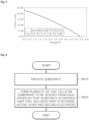
- FIG. 6 is a flowchart showing a method of forming a solar cell according to an embodiment of the present invention.
- the solar cell according to the present embodiment provides the solar cell structure suitable for low-illuminance environments.
- the efficiency loss of the solar cell increases in proportion to the amount of current generated and the moving distance of carriers. According to the present embodiment, it is possible to propose a structure capable of solving the problems of the dead space and leakage current of the conventional solar cell in a low-illuminance environment, and provide a solar cell design capable of minimizing efficiency loss due to voltage drop.
- a substrate is provided (S610).
- a plurality of unit cells is formed on the substrate to be spaced from each other so that the substrate is exposed (S620).
- connection electrode that connects a plurality of unit cells may be formed.
- the connection electrode contacts an electrode of a unit cell with the opposite electrode of a neighboring unit cell to connect the unit cells.
- connection electrode according to the present embodiment is not disposed in an insulating structure or a non-power generation area between the unit cells, but extends from the second electrode and is connected to the neighboring unit cell.
- the unit cell includes a first electrode, an active layer, and a second electrode.
- the first electrode is formed on a substrate
- the active layer is formed on the first electrode
- the second electrode is formed on the active layer.
- a one-time scribing process may be performed.
- FIG. 7 is a diagram showing in detail a first process of the method of forming the unit cells of the solar cell, according to an embodiment of the present invention.
- the first electrode is deposited on the substrate (S710).
- the first electrode may be a transparent electrode.
- the active layer is formed on the first electrode (S720).
- the active layer is formed using a transfer, deposition or coating method.
- the second electrode is formed on the active layer (S730).
- each unit cell includes the first electrode, the active layer, and the second electrode.
- connection electrode is formed (S750).
- FIG. 8 is a diagram showing in detail a second process of the method of forming the unit cell of the solar cell, according to an embodiment of the present invention.
- the first electrode is deposited on the substrate (S810) .
- the active layer is formed on the first electrode (S820).
- the active layer is formed using a transfer, deposition or coating method.
- each unit cell includes the first electrode and the active layer.
- the second electrode and the connection electrode are formed on the active layer (S840) .
- the second electrode is formed through patterning.
- the connection electrode is also formed through patterning.
- FIG. 9 is a diagram showing in detail a third process of the method of forming the unit cells of the solar cell, according to an embodiment of the present invention.
- the first electrode is deposited on the substrate (S910).
- each unit cell includes the first electrode.
- the active layer is formed on the first electrode (S930).
- the active layer is formed through patterning.
- the second electrode and the connection electrode are formed on the active layer (S940).
- the second electrode is formed through patterning.
- the connection electrode is also formed through patterning.
Landscapes
- Physics & Mathematics (AREA)
- Electromagnetism (AREA)
- Engineering & Computer Science (AREA)
- Manufacturing & Machinery (AREA)
- Chemical & Material Sciences (AREA)
- Inorganic Chemistry (AREA)
- Materials Engineering (AREA)
- Photovoltaic Devices (AREA)
- Electroluminescent Light Sources (AREA)
Abstract
Description
- The present invention relates to a solar cell and a method of forming the same, and more specifically, to a solar cell having an insulating structure or a non-power generation area in which unit cells are spaced from each other and a substrate is exposed, and a method of forming the same.
- A solar cell is a device that directly converts solar energy into electrical energy by applying the photovoltaic effect. Such a solar cell may be divided into an inorganic solar cell and an organic solar cell depending on materials of a thin film.
- In the organic/inorganic solar cells, an electrode structure that collects electrons and holes is more important in a module structure in which multiple cells are connected than in a single unit cell.
- In particular, in the case of various solar cell modules (e.g., OPV, CIGS, PSC, etc.) that adopt a monolithic process, each cell to form the module is formed by a plurality of scribing (e.g., LASER scribing) processes.
-
FIG. 1 is a diagram schematically showing a structure of a plurality of cell electrodes of a conventional solar cell. - In the conventional solar cell, as shown in
FIG. 1 , respective layers that form an electrode layer and an activating layer are connected in a step form. - The conventional structure needs a scribing process for each layer due to the step structure, and a series-
connection electrode 150 that connects a lowerfirst electrode 120 and anupper second electrode 140 is disposed between cells. - However, due to the connection electrode disposed between the cells, a problem occurs in that a dead space increases.
- The step structure of the conventional solar cell increases leakage current between the cells as well as the increase of the dead space, resulting in a negative impact on device properties.
- Therefore, the present invention has been made in view of the above problems, and it is an object of the present invention to provide a solar cell having an insulating structure or a non-power generation area in which unit cells are spaced from each other and a substrate is exposed, and a method of forming the same.
- In accordance with an aspect of the present invention, the above and other objects can be accomplished by the provision of a solar cell including: a substrate; and a plurality of unit cells that are formed on the substrate and include a first electrode, an active layer, and a second electrode, in which the unit cells are spaced from each other.
- The unit cells may be spaced from each other at intervals ranging from 0.1 mm to 2 mm.
- At least one of the first electrode or the second electrode may be a transparent electrode.
- The solar cell may be provided for low illuminance of 100 to 10,000 lux.
- The solar cell may further include a connection electrode that connects the unit cells.
- The connection electrode may extend from the second electrode, and may be connected to the first electrode of a neighboring unit cell.
- The second electrode and the connection electrode may be made of the same material.
- The second electrode and the connection electrode may be formed in an integrated structure.
- The first electrode and the second electrode may be each made of one or more of indium tin oxide (ITO), fluorine tin oxide (FTO), antimony tin oxide (ATO), zinc oxide, tin oxide, ZnoGa2O3, ZnO-Al2O3, platinum, ruthenium, palladium, iridium, rhodium (Rh), osmium (Os), carbon (C), WO3, TiO2, Au, Cu, Ag, In, Ru, Pd, Ir, graphene, and conductive polymer.
- The connection electrode may be made of one or more of indium tin oxide (ITO), fluorine tin oxide (FTO), antimony tin oxide (ATO), zinc oxide, tin oxide, ZnoGa2O3, ZnO-Al2O3, platinum, ruthenium, palladium, iridium, rhodium (Rh), osmium (Os), carbon (C), WO3, TiO2, Au, Cu, Ag, In, Ru, Pd, Ir, graphene, and conductive polymer.
- The active layer may include at least one of an activating layer, an electron transporting layer, or a hole transporting layer.
- The activating layer may include a perovskite light absorption layer.
- The solar cell may further include a battery disposed in a spaced portion between the unit cells.
- In accordance with another aspect of the present invention, there is provided a method of forming a solar cell, including providing a substrate, and forming a plurality of unit cells on the substrate to be spaced from each other so that the substrate is exposed, in which the unit cell includes a first electrode, an active layer, and a second electrode.
- The forming the unit cells includes a single scribing process.
- The method may further include forming a connection electrode that connects the plurality of unit cells.
- The forming the unit cells may include forming the first electrode on the substrate, forming the active layer on the first electrode, and forming the second electrode on the active layer.
- According to the solar cell and the method of forming the same according to the present invention, it is possible to minimize leakage current by disposing unit cells to be spaced from each other to expose a substrate and providing insulation between unit cells.
- Further, it is possible to increase the power generation efficiency of a solar cell device through minimizing an insulating structure or a non-power generation area.
- Further, it is possible to achieve process simplification by forming an insulating structure through a single scribing process, thereby reducing process costs.
- In addition, it is possible to decreasing power and efficiency losses, especially during low-illuminance power generation.
-
-
FIG. 1 is a diagram schematically showing a structure of a plurality of cell electrodes of a conventional solar cell. -
FIG. 2 is a diagram showing a schematic diagram of a solar cell according to an embodiment of the present invention. -
FIG. 3 is a perspective view showing connection electrodes in a solar cell according to an embodiment of the present invention. -
FIG. 4 is a diagram showing measurement results in a low-illuminance environment of a solar cell according to an embodiment of the present invention. -
FIG. 5 is a diagram showing 1 sun (outdoor) measurement results of the solar cell according to an embodiment of the present invention. -
FIG. 6 is a flowchart showing a method of forming a solar cell according to an embodiment of the present invention. -
FIG. 7 is a diagram showing a first process in the method of forming unit cells of the solar cell inFIG. 6 . -
FIG. 8 is a diagram showing a second process in the method of forming the unit cells of the solar cell inFIG. 6 . -
FIG. 9 is a diagram showing a third process in the method of forming the unit cells of the solar cell inFIG. 6 . - Hereinafter, preferred embodiments of the present invention will be described with reference to the accompanying drawings. Embodiments of the present invention may be modified into various other forms, and the scope of the invention is not limited to the embodiments described below. The embodiments of the present invention are provided to more specifically describe the invention to those skilled in the art. Accordingly, shapes and sizes of elements in the drawings may be exaggerated for clear description, and elements represented by the same reference numerals in the drawings are the same elements.
- In the present description, a solar cell refers to a module structure in which a plurality of unit cells is connected in a narrow sense, but refers to a device including the module structure and other components such as a battery in a broad sense. In other words, the solar cell according to the embodiments of the present invention may refer to a photovoltaics system, which may include a component that receives light and converts the light into electricity (a solar cell in a narrow sense), and may further include a device such as a battery capable of converting generated electricity into a specific form or storing the generated electricity (a solar cell in a broad sense).
- In the present invention, an insulating structure or a non-power generation area refers to a structure or an area where a substrate is exposed between unit cells. Unlike the conventional solar cell in which a connection electrode is disposed between unit cells, the solar cell according to the present invention has an insulating structure in which a substrate is exposed to minimize leakage current and minimize a non-power generation area.
- As an example, the solar cell may be a monolithic solar cell. A monolithic device refers to a device in which various devices are integrated and stacked on one substrate.
-
FIG. 2 is a diagram showing a schematic diagram of a solar cell according to an embodiment of the present invention. - For clarity of description,
FIG. 2 mainly shows a module structure of an electrode structure, but may include other components not shown. - Referring to
FIG. 2 , a solar cell according to the present embodiment includes asubstrate 210 and a plurality of unit cells. In the case of a crystalline silicon solar cell, the substrate of the solar cell may be a silicon wafer, and the solar cell is manufactured by forming junctions and electrodes thereon. In the case of a thin film solar cell, the substrate of the solar cell may be a support on which a thin film grows, which may be made of glass, plastics, stainless steel, etc. The substrate is a plate member that maintains a mechanical strength of a photovoltaic generation module. As another example, thesubstrate 210 may be a semiconductor substrate made of a compound such as GaN. - The
substrate 210 is generally transparent to allow incidence of external light, but may be opaque depending on a counter electrode. As an example, the substrate may be made of transparent glass or plastics. Specific examples of plastics include polyethylene terephthalate (PET), polyethylene naphthalate (PEN), polycarbonate (PC), polypropylene (PP), polyimide (PI), tri acetyl cellulose (TAC), or the like. - The substrate of the solar cell according to the present embodiment may be a flexible substrate, instead of a rigid substrate such as a semiconductor wafer or glass. The flexible substrate may include a metal flexible substrate, an ultra-thin glass substrate, a plastic substrate, or the like.
- The unit cell may include a
first electrode 220, anactive layer 230, and asecond electrode 240. - The basic unit of the solar cell is a unit cell. Since voltage output from one cell is very small, within about 1 Volt, a power generator manufactured by connecting multiple unit cells in series and parallel and packaging them in one piece to obtain voltage and output within a practical range may be provided.
- Specifically, an aspect ratio of the unit cell, the ratio of a horizontal width to a vertical length, is 8 or less. Here, the horizontal width (short side in
FIG. 3 ) refers to a side of the unit cell where the connection electrode is formed, and the vertical length (long side inFIG. 3 ) refers to a side on which scribing is performed in the unit cell. In a case where the aspect ratio is set to 8 or less, there is an advantage that the power generation efficiency of the solar cell increases to the same level or higher than that of the conventional solar cell in the case of 1 sun (outdoor) measurement. - Respective unit cells of the solar cell according to the present invention are disposed to be spaced from each other to expose the substrate. The width of an
exposure portion 250 of the substrate between the unit cells may be in the range of 0.1 mm to 2 mm or 0.1 mm to 1 mm. By adjusting the width of theexposure portion 250 to the above range, the power generation area per unit area may be increased, compared to the conventional solar cell. - The insulating structure between the unit cells may be formed by, ideally, a single scribing process (for example, laser or physical scribing).
- Here, by arranging the insulating structure on the exposure portion of the substrate between the unit cells, the unit cells may be completely physically shortcircuited, thereby minimizing leakage current.
- Here, the width of the insulating structure between the unit cells may be the same.
- Alternatively, the widths of the insulating structures between the unit cells are not the same and may differ from each other within an allowable error range.
- Here, the insulating structure may be formed to be exposed to the air, or may be covered with an insulating material. In particular, in a case where a vacuum cannot be maintained for a final product, the insulating structure may be covered with the insulating material.
- In the conventional solar cell in which connection electrodes are disposed between the unit cells shown in
FIG. 1 , in the case of a module with a unit cell width of 1 cm, the non-power generation area where the connection electrodes are disposed in manufacturing the module through multi-layer scribing must be secured to be equal to or greater than approximately 1 mm. In contrast, the width of the insulating structure where the substrate is exposed between the unit cells according to the present embodiment is at least 0.1 mm. As a result, the width of the insulating structure or the non-power generation area is reduced to 1/10 compared to the conventional solar cell. As the width of the non-power generation area decreases, the amount of power generation per unit area increases. In the solar cell according to the present embodiment, the insulating structure between the unit cells may have a width of 2 mm or less. - The insulating structure between the unit cells may be formed by performing patterning to form fine gaps between the unit cells. The patterning is performed to partially remove thin films formed on a glass substrate, and is mainly achieved by laser scribing. The scribing method is not limited to the laser scribing, and may also be achieved by other physical scribing methods.
- In a case where the patterning is performed using the laser scribing, the width of the insulating structure may be determined by the resolution of a laser beam at the wavelength used.
- In a modified embodiment, the solar cell of the present embodiment may have batteries individually disposed in spaced portions.
- The advantage of the solar cell-battery integrated device is that the battery can be continuously used under sunlight without a separate charging method.
- Specifically, in order to increase the power generation efficiency, the solar cell according to the present embodiment may have a configuration in which the battery is disposed in the insulating structure in which the substrate is exposed between the unit cells. In the case of this battery disposition, the width of the spaced portion may increase.
- The
active layer 230 of the solar cell according to the present embodiment includes at least one of an activating layer, an electron transporting layer, or a hole transporting layer. - As an example, the
active layer 230 may include the activating layer, the electron transporting layer, and the hole transporting layer. As another example, theactive layer 230 may include the electron transporting layer and the activating layer. As still another example, theactive layer 230 may include the activating layer. - The hole transporting layer is a layer that helps smooth transport of holes between the first electrode and the activating layer.
- The hole transporting layer may be made of a single molecule hole transport material (spiro-MeoTAD [2,2',7,7'-tetrakis (N,N-p-dimethoxy-phenylamino)-9,9'-spirobifluorene]) or a polymer hole transport material (P3HT [poly (3-hexylthiophene)].
- The electron transporting layer is a layer that helps smooth transport of electrons between the second electrode and the activating layer.
- The electron transporting layer may be made of metal oxide semiconductor (TiO2, SnO2) or PCBM (phenyl-C61-butyric acid methyl ester).
- The activating layer may include a perovskite light absorption layer, and in this case, it is possible to achieve high photoelectric conversion efficiency.
- The light absorption layer serves to absorb external light on the surface of metal oxide particles to generate electrons. A material that shows excellent photoelectric conversion efficiency as the light absorption layer may be methyl ammonium lead iodide (CH3NH3PbI3) compound, which is known to absorb light between approximately 400 nm and 800 nm.
- A material with a perovskite crystal structure that serves as the light absorption layer is a mixture of inorganic and organic materials and has a molecular formula AMX3. Representative examples thereof may include the above-mentioned methyl ammonium lead iodide (CH3NH3PbI3, MAPbI3) or formamidinium lead iodide (CH(NH2)2PbI3, FAPbI3). In the molecular formula of AMX3, "A" represents an organic cation, "M" represents a metal cation, and "X" represents a halogen anion. An organic/organic hybrid halide containing the above ingredients shows high photoelectric conversion efficiency when used as the light absorption layer in the solar cell due to its unique crystallization behavior and photoelectric properties.
- Organic/inorganic hybrid perovskite materials have excellent photoelectric properties such as a high visible light absorption coefficient, ease of bandgap control, excellent charge mobility, and a long charge diffusion length, and may show high efficiency of 25% or higher when used as light absorption materials for solar cells. The perovskite materials having these excellent properties may effectively absorb visible light of indoor lighting and photoelectrically convert the light, thereby showing excellent efficiency even in low-illuminance environments.
- According to the present embodiment, the solar cell may have a thickness less than 10 um. Specifically, the solar cell according to the present embodiment may have a thickness of 500 nm or greater and less than 5 um. In a case where the thickness of the solar cell is too thin, there is no problem when forming electrodes, but the thickness of the light absorption layer may become thin, which may result in decrease in photoelectric efficiency. In the case of PSC, the light absorption layer may have a thickness of 300 nm to 500 nm. Therefore, considering the thickness of the counter electrode and the electron/hole absorption layer, the lower limit of the thickness is preferably about 500 nm or greater.
- Compared to the thickness of a conventional dye-sensitized solar cell (DSC) of about 10 to 20 um, the solar cell according to the present embodiment is advantageous in that it can provide a solar cell with a thinner thickness.
-
FIG. 3 shows a solar cell including connection electrodes according to an embodiment of the present invention. - In a case where solar cells are connected in series, the voltage increases in proportion to the number of cells, and in a case where the solar cells are connected in parallel, the current increases. Using this principle, it is possible to manufacture a module with desired voltage and current.
- Referring to the drawings, the solar cell of the present embodiment may further include a
connection electrode 360 that connects unit cells. The connection electrode may extend from thesecond electrode 340 of the unit cell, and may be connected to the first electrode of a neighboring unit cell. The solar cell of the present embodiment may include a contact metal that is patterned and then heat-treated to minimize contact resistance when connecting the connection electrode with the first electrode of the neighboring unit cell. - In this embodiment, the
second electrode 340 and the connection electrode may be made of the same material, so that contact resistance is minimized. - Further, the second electrode and the connection electrode may be formed as an integrated structure, and the integrated structure may be formed by depositing the second electrode and the connection electrode at the same time, thereby shortening the process.
- The second electrode and the connection electrode may be formed as the integrated structure through a patterning process.
- In this embodiment, at least one of the first electrode or the second electrode may be provided as a transparent electrode. That is, at least one of the first electrode or the second electrode must be a transparent electrode.
- In a case where both the first and second electrodes are transparent electrodes, it is possible to provide a semi-transparent solar cell, and in a case where only one of the first and second electrodes is a transparent electrode, it is possible to provide a highly efficient solar cell with minimized efficiency loss.
- Here, the transparent electrode refers to an electrode formed on the surface of a solar cell on which light is incident and having high light transmittance and high electrical conductivity.
- The
first electrode 320 and thesecond electrode 340 are each made of one or more of indium tin oxide (ITO), fluorine tin oxide (FTO), antimony tin oxide (ATO), zinc oxide, tin oxide, ZnoGa2O3, ZnO-Al2O3, platinum, ruthenium, palladium, iridium, rhodium (Rh), osmium (Os), carbon (C), WO3, TiO2, Au, Cu, Ag, In, Ru, Pd, Ir, graphene, and conductive polymer. - The connection electrode is made of one or more of indium tin oxide (ITO), fluorine tin oxide (FTO), antimony tin oxide (ATO), zinc oxide, tin oxide, ZnoGa2O3, ZnO-Al2O3, platinum, ruthenium, palladium, iridium, rhodium (Rh), osmium (Os), carbon (C), WO3, TiO2, Au, Cu, Ag, In, Ru, Pd, Ir, graphene, and conductive polymer.
- In this embodiment, the first electrode may be made of fluorine tin oxide (FTO), and the second electrode and the connection electrode may be made of metal, for example, gold (Au). In this case, it is possible to implement a solar cell with superior efficiency.
-
FIG. 4 shows measurement results of the solar cell of the present embodiment in a low-illuminance environment. - Referring to
FIG. 4 , in a case where the insulating structure is disposed between the unit cells according to the embodiment of the present invention, the solar cell may show excellent characteristics with an FF (fill factor) of 64% or higher at low illuminance (1,000 lux or less). - Recently, as the demand for indoor Internet of Things (IoT) sensors that can be driven with low power (average 20 to 50 uW) has increased exponentially, the need to develop a wireless power system that can generate and supply power in an indoor low-illuminance environment has emerged.
- In general, indoor lighting illuminance of residential and commercial buildings is equal to or lower than 5.0*10-2 mW/cm2 (200 to 1000 lux), which is very lower than the standard light intensity driven by a solar cell (1 Sun, 100 mW/cm2). Accordingly, power loss due to interfacial defects and charge traps, which does not appear under solar cell standard test conditions (STC), may appear as serious problems under low-illuminance light sources, and thus, the solar cell device structure optimized under the solar cell standard test conditions (STC) may not guarantee high efficiency in the indoor low-illuminance environment.
- As described above, the solar cell according to the embodiment of the present invention can minimize leakage current by providing insulation between unit cells, which may be a desirable alternative to a low-illuminance solar cell that can generate power in the indoor low-illuminance environment.
- In this embodiment, the solar cell is intended for low illuminance of 100 to 10,000 lux. Specifically, in a case where the solar cell is used for low illuminance of 100 to 1,500 lux, and more specifically, for low illuminance of 200 to 800 lux.
-
FIG. 5 shows 1 sun (outdoor) measurement results of the solar cell according to an embodiment of the present invention. - According to the solar cell of the present embodiment, it is possible to minimize leakage current by providing insulation between unit cells. Accordingly, it is possible to provide an optimization principle and mechanism of a device structure for solar cell development under a low-illuminance indoor lighting condition.
- However, in the solar cell having the insulating structure between the unit cells according to the present embodiment, in a case where the activating layer includes a perovskite light absorption layer of 10 cm2 in
FIG. 5 , the FF is 29% in 1 sun (outdoor) measurement, which shows a bad result. - This is largely influenced by the voltage drop resulting from the sheet resistance of the first and second electrodes. In fact, high density carriers (electrons, holes) generated at high illuminance show a high current value, and result in large power loss in a case where the sheet resistance is the same at Ploss = I2R. However, since the current value is relatively low in low illuminance, power loss has relatively less impact on the solar cell structure.
- Referring to
FIGs. 4 and5 , the solar cell having the insulating structure between the unit cells according to the present embodiment is suitable for low-illuminance environments, and may not be suitable for use in 1 sun (outdoor), that is, outdoors. -
FIG. 6 is a flowchart showing a method of forming a solar cell according to an embodiment of the present invention. - As described with reference to
FIG. 4 , the solar cell according to the present embodiment provides the solar cell structure suitable for low-illuminance environments. - In fact, the efficiency loss of the solar cell increases in proportion to the amount of current generated and the moving distance of carriers. According to the present embodiment, it is possible to propose a structure capable of solving the problems of the dead space and leakage current of the conventional solar cell in a low-illuminance environment, and provide a solar cell design capable of minimizing efficiency loss due to voltage drop.
- In a method of forming the solar cell according to an embodiment of the present invention, first, a substrate is provided (S610).
- Then, a plurality of unit cells is formed on the substrate to be spaced from each other so that the substrate is exposed (S620).
- In addition, a connection electrode that connects a plurality of unit cells may be formed. The connection electrode contacts an electrode of a unit cell with the opposite electrode of a neighboring unit cell to connect the unit cells.
- The connection electrode according to the present embodiment is not disposed in an insulating structure or a non-power generation area between the unit cells, but extends from the second electrode and is connected to the neighboring unit cell.
- The unit cell includes a first electrode, an active layer, and a second electrode. In providing the unit cells, the first electrode is formed on a substrate, the active layer is formed on the first electrode, and the second electrode is formed on the active layer.
- In providing the unit cells in step S620, a one-time scribing process may be performed.
-
FIG. 7 is a diagram showing in detail a first process of the method of forming the unit cells of the solar cell, according to an embodiment of the present invention. - First, the first electrode is deposited on the substrate (S710). The first electrode may be a transparent electrode.
- Then, the active layer is formed on the first electrode (S720). The active layer is formed using a transfer, deposition or coating method.
- Then, the second electrode is formed on the active layer (S730).
- Subsequently, an insulating structure is formed in which the substrate is exposed between the unit cells through a scribing (laser or physical) process (S740). In step S740, each unit cell includes the first electrode, the active layer, and the second electrode.
- Then, a connection electrode is formed (S750).
-
FIG. 8 is a diagram showing in detail a second process of the method of forming the unit cell of the solar cell, according to an embodiment of the present invention. - First, the first electrode is deposited on the substrate (S810) .
- Then, the active layer is formed on the first electrode (S820). The active layer is formed using a transfer, deposition or coating method.
- Then, an insulating structure is formed in which the substrate is exposed between the unit cells through a scribing (laser or physical) process (S830). In step S830, each unit cell includes the first electrode and the active layer.
- Then, the second electrode and the connection electrode are formed on the active layer (S840) . Here, the second electrode is formed through patterning. The connection electrode is also formed through patterning.
-
FIG. 9 is a diagram showing in detail a third process of the method of forming the unit cells of the solar cell, according to an embodiment of the present invention. - First, the first electrode is deposited on the substrate (S910).
- Then, an insulating structure is formed in which the substrate is exposed between the unit cells through a scribing (laser or physical) process (S920). In step S920, each unit cell includes the first electrode.
- Then, the active layer is formed on the first electrode (S930). The active layer is formed through patterning.
- Then, the second electrode and the connection electrode are formed on the active layer (S940). Here, the second electrode is formed through patterning. The connection electrode is also formed through patterning.
- The terms used in the present description are intended to describe specific embodiments, and are not intended to limit the invention. Unless it is clear from the context, singular expressions should be considered to have a plural meaning. Terms such as "include", "comprise", "have", and the like should not be interpreted to exclude additional elements other than elements described in the specification.
- The invention is not limited by the above-described embodiments and the attached drawings, but should be defined by the attached claims. Accordingly, various forms of substitutions, modifications, and changes may be made by those skilled in the art without departing from the technical spirit of the invention as set forth in the claims, and these are also considered to fall within the scope of the invention.
Claims (17)
- A solar cell comprising:a substrate; anda plurality of unit cells that are formed on the substrate and include a first electrode, an active layer, and a second electrode,wherein the unit cells are spaced from each other.
- The solar cell according to claim 1, wherein the unit cells are spaced from each other at intervals ranging from 0.1 mm to 2 mm.
- The solar cell according to claim 1, wherein at least one of the first electrode or the second electrode is a transparent electrode.
- The solar cell according to claim 1, wherein the solar cell is provided for low illuminance of 100 lux to 10,000 lux.
- The solar cell according to claim 1, further comprising: a connection electrode that connects the unit cells.
- The solar cell according to claim 5, wherein the connection electrode extends from the second electrode, and is connected to the first electrode of a neighboring unit cell.
- The solar cell according to claim 5, wherein the second electrode and the connection electrode are made of the same material.
- The solar cell according to claim 6, wherein the second electrode and the connection electrode are formed in an integrated structure.
- The solar cell according to claim 1, wherein the first electrode and the second electrode are each made of one or more of indium tin oxide (ITO), fluorine tin oxide (FTO), antimony tin oxide (ATO), zinc oxide, tin oxide, ZnoGa2O3, ZnO-Al2O3, platinum, ruthenium, palladium, iridium, rhodium (Rh), osmium (Os), carbon (C), WO3, TiO2, Au, Cu, Ag, In, Ru, Pd, Ir, graphene, and conductive polymer.
- The solar cell according to claim 5, wherein the connection electrode is made of one or more of indium tin oxide (ITO), fluorine tin oxide (FTO), antimony tin oxide (ATO), zinc oxide, tin oxide, ZnoGa2O3, ZnO-Al2O3, platinum, ruthenium, palladium, iridium, rhodium (Rh), osmium (Os), carbon (C), WO3, TiO2, Au, Cu, Ag, In, Ru, Pd, Ir, graphene, and conductive polymer.
- The solar cell according to claim 1, wherein the active layer includes at least one of an activating layer, an electron transporting layer, or a hole transporting layer.
- The solar cell according to claim 11, wherein the activating layer includes a perovskite light absorption layer.
- The solar cell according to claim 1, further comprising: a battery disposed in a spaced portion between the unit cells.
- A method of forming a solar cell, comprising:providing a substrate; andforming a plurality of unit cells on the substrate to be spaced from each other so that the substrate is exposed,wherein each unit cell includes a first electrode, an active layer, and a second electrode.
- The method according to claim 14, wherein the forming the unit cells includes a single scribing process.
- The method according to claim 14, further comprising:
forming a connection electrode that connects the plurality of unit cells. - The method according to claim 14, wherein the forming the unit cells includes:forming the first electrode on the substrate;forming the active layer on the first electrode; andforming the second electrode on the active layer.
Applications Claiming Priority (2)
| Application Number | Priority Date | Filing Date | Title |
|---|---|---|---|
| KR1020210193377A KR102964118B1 (en) | 2021-12-30 | Solar cell and method of forming the same | |
| PCT/KR2022/020194 WO2023128396A1 (en) | 2021-12-30 | 2022-12-13 | Solar cell and method for forming same |
Publications (2)
| Publication Number | Publication Date |
|---|---|
| EP4460164A1 true EP4460164A1 (en) | 2024-11-06 |
| EP4460164A4 EP4460164A4 (en) | 2025-10-08 |
Family
ID=86999538
Family Applications (1)
| Application Number | Title | Priority Date | Filing Date |
|---|---|---|---|
| EP22916541.0A Pending EP4460164A4 (en) | 2021-12-30 | 2022-12-13 | SOLAR CELL AND METHOD FOR MANUFACTURING SAME |
Country Status (4)
| Country | Link |
|---|---|
| US (1) | US20240324258A1 (en) |
| EP (1) | EP4460164A4 (en) |
| JP (2) | JP2024545759A (en) |
| WO (1) | WO2023128396A1 (en) |
Family Cites Families (15)
| Publication number | Priority date | Publication date | Assignee | Title |
|---|---|---|---|---|
| JPS5935487A (en) * | 1982-08-24 | 1984-02-27 | Sanyo Electric Co Ltd | Method for manufacturing optical semiconductor devices |
| JPS59198775A (en) * | 1983-04-26 | 1984-11-10 | Fuji Electric Co Ltd | Solar battery |
| JP2010010606A (en) * | 2008-06-30 | 2010-01-14 | Hitachi Maxell Ltd | Optical conversion element cell, integrated optical conversion device, method of manufacturing optical conversion element cell, and method of manufacturing integratedoptical conversion device |
| SG178410A1 (en) * | 2009-08-20 | 2012-04-27 | Univ Nanyang Tech | Integrated electrode architectures for energy generation and storage |
| KR101055980B1 (en) * | 2010-05-17 | 2011-08-11 | 주성엔지니어링(주) | Thin film type solar cell and manufacturing method thereof |
| JP5991092B2 (en) * | 2012-09-04 | 2016-09-14 | 大日本印刷株式会社 | Method for producing organic solar cell module |
| JP2016051805A (en) * | 2014-08-29 | 2016-04-11 | ローム株式会社 | ORGANIC THIN FILM SOLAR CELL, ITS MANUFACTURING METHOD, ELECTRONIC DEVICE |
| JP2016058455A (en) * | 2014-09-05 | 2016-04-21 | 株式会社東芝 | Photoelectric conversion element, wiring board for photoelectric conversion element, manufacturing method of photoelectric conversion element, and photoelectric conversion structure |
| TWM556022U (en) * | 2017-09-04 | 2018-02-21 | Nanobit Tech Co Ltd | Photovoltaic cell structure |
| KR102130778B1 (en) * | 2018-07-10 | 2020-07-08 | 울산과학기술원 | Perovskite solar cell module |
| KR102192312B1 (en) * | 2019-01-30 | 2020-12-18 | 금오공과대학교 산학협력단 | Producing Method of Inverted Organic Solar Cell Module with Uniform Cell Performance |
| KR102779834B1 (en) * | 2019-06-04 | 2025-03-12 | 주성엔지니어링(주) | Substrate for Solar cell and Solar Cell and Method of Manufacturing Solar cell |
| CN113272987B (en) * | 2019-12-12 | 2024-07-23 | 株式会社安能科多科技 | Component manufacturing method |
| CN113646913A (en) * | 2020-03-10 | 2021-11-12 | 株式会社东芝 | Photoelectric conversion device |
| KR20210144104A (en) * | 2020-05-21 | 2021-11-30 | 한국전자통신연구원 | Perovskite solar cell module |
-
2022
- 2022-12-13 EP EP22916541.0A patent/EP4460164A4/en active Pending
- 2022-12-13 WO PCT/KR2022/020194 patent/WO2023128396A1/en not_active Ceased
- 2022-12-13 JP JP2024537012A patent/JP2024545759A/en active Pending
-
2024
- 2024-05-30 US US18/678,236 patent/US20240324258A1/en active Pending
-
2025
- 2025-11-25 JP JP2025203117A patent/JP2026020303A/en active Pending
Also Published As
| Publication number | Publication date |
|---|---|
| JP2024545759A (en) | 2024-12-11 |
| WO2023128396A1 (en) | 2023-07-06 |
| US20240324258A1 (en) | 2024-09-26 |
| EP4460164A4 (en) | 2025-10-08 |
| KR20230102906A (en) | 2023-07-07 |
| JP2026020303A (en) | 2026-02-06 |
Similar Documents
| Publication | Publication Date | Title |
|---|---|---|
| Bailie et al. | Semi-transparent perovskite solar cells for tandems with silicon and CIGS | |
| EP4432810A1 (en) | Perovskite silicon-based laminated solar cell and manufacturing method therefor | |
| KR101117127B1 (en) | Tandem solar cell using amorphous silicon solar cell and organic solar cell | |
| CN111430384B (en) | A solar cell module, a laminated solar cell and a manufacturing method thereof | |
| US20080121264A1 (en) | Thin film solar module and method of fabricating the same | |
| US20180315871A1 (en) | Vertically stacked photovoltaic and thermal solar cell | |
| JP2018517304A (en) | Method for depositing perovskite materials | |
| US12628490B2 (en) | Solar cell | |
| US20240251573A1 (en) | Methods of manufacturing a perovskite optoelectronic device | |
| US20090255585A1 (en) | Flexible photovoltaic device | |
| CN116913991B (en) | Heterojunction solar cell, preparation method thereof, photovoltaic module and photovoltaic system | |
| Nikbakht et al. | Upscaling Perovskite Photovoltaics: from 156 cm2 Modules to 0.73 M2 Panels | |
| US8981388B2 (en) | Solar cell and method of manufacturing the same | |
| CN111916561A (en) | Perovskite solar cell, tandem solar cell and battery pack | |
| WO2007138348A2 (en) | Photovoltaic cell with mesh electrode | |
| KR20220077980A (en) | Perovskite photovoltaic cell with high-efficiency and preparing method of the same | |
| US20240324258A1 (en) | Solar cell and method of forming the same | |
| KR102964118B1 (en) | Solar cell and method of forming the same | |
| KR101462356B1 (en) | Dye sensitized solar cell and method of fabricating the same | |
| US20220077412A1 (en) | Solar cell module | |
| JP4314847B2 (en) | Dye-sensitized solar cell module | |
| US20170141246A1 (en) | Titanium oxide having hexagonal column shape, method of fabricating the same, solar cell including the same, and method of fabricating solar cell including the same | |
| JP2009009851A (en) | Photoelectric conversion device | |
| CN120813159B (en) | A perovskite stacked assembly and its preparation method | |
| CN118338689B (en) | Solar cell and method for manufacturing the same |
Legal Events
| Date | Code | Title | Description |
|---|---|---|---|
| STAA | Information on the status of an ep patent application or granted ep patent |
Free format text: STATUS: THE INTERNATIONAL PUBLICATION HAS BEEN MADE |
|
| PUAI | Public reference made under article 153(3) epc to a published international application that has entered the european phase |
Free format text: ORIGINAL CODE: 0009012 |
|
| STAA | Information on the status of an ep patent application or granted ep patent |
Free format text: STATUS: REQUEST FOR EXAMINATION WAS MADE |
|
| 17P | Request for examination filed |
Effective date: 20240617 |
|
| AK | Designated contracting states |
Kind code of ref document: A1 Designated state(s): AL AT BE BG CH CY CZ DE DK EE ES FI FR GB GR HR HU IE IS IT LI LT LU LV MC ME MK MT NL NO PL PT RO RS SE SI SK SM TR |
|
| DAV | Request for validation of the european patent (deleted) | ||
| DAX | Request for extension of the european patent (deleted) | ||
| REG | Reference to a national code |
Ref country code: DE Ref legal event code: R079 Free format text: PREVIOUS MAIN CLASS: H10K0030000000 Ipc: H10K0039120000 |
|
| A4 | Supplementary search report drawn up and despatched |
Effective date: 20250909 |
|
| RIC1 | Information provided on ipc code assigned before grant |
Ipc: H10K 39/12 20230101AFI20250903BHEP Ipc: H10K 30/40 20230101ALI20250903BHEP Ipc: H10K 71/20 20230101ALI20250903BHEP |