EP4459682A1 - Verfahren zur herstellung einer photovoltaischen vorrichtung mit mehreren übergängen, die eine gaasbi unterzelle umfasst - Google Patents
Verfahren zur herstellung einer photovoltaischen vorrichtung mit mehreren übergängen, die eine gaasbi unterzelle umfasst Download PDFInfo
- Publication number
- EP4459682A1 EP4459682A1 EP23171311.6A EP23171311A EP4459682A1 EP 4459682 A1 EP4459682 A1 EP 4459682A1 EP 23171311 A EP23171311 A EP 23171311A EP 4459682 A1 EP4459682 A1 EP 4459682A1
- Authority
- EP
- European Patent Office
- Prior art keywords
- gaasbi
- subcell
- subcells
- contact layer
- photovoltaic device
- Prior art date
- Legal status (The legal status is an assumption and is not a legal conclusion. Google has not performed a legal analysis and makes no representation as to the accuracy of the status listed.)
- Pending
Links
- 238000000034 method Methods 0.000 title claims abstract description 29
- 239000000956 alloy Substances 0.000 claims abstract description 36
- 229910045601 alloy Inorganic materials 0.000 claims abstract description 35
- 229910000530 Gallium indium arsenide Inorganic materials 0.000 claims abstract description 27
- 239000000758 substrate Substances 0.000 claims abstract description 20
- 239000013078 crystal Substances 0.000 claims abstract description 11
- 239000004065 semiconductor Substances 0.000 claims abstract description 11
- 229910001218 Gallium arsenide Inorganic materials 0.000 claims description 28
- 229910052797 bismuth Inorganic materials 0.000 claims description 9
- 229910052733 gallium Inorganic materials 0.000 claims description 9
- 229910052738 indium Inorganic materials 0.000 claims description 9
- 229910000980 Aluminium gallium arsenide Inorganic materials 0.000 claims description 8
- 229910052782 aluminium Inorganic materials 0.000 claims description 6
- 229910052787 antimony Inorganic materials 0.000 claims description 6
- 229910052785 arsenic Inorganic materials 0.000 claims description 6
- 229910052757 nitrogen Inorganic materials 0.000 claims description 5
- 229910052732 germanium Inorganic materials 0.000 claims 5
- 229910052710 silicon Inorganic materials 0.000 claims 5
- 229910052698 phosphorus Inorganic materials 0.000 claims 4
- 229910052718 tin Inorganic materials 0.000 claims 4
- 229910005540 GaP Inorganic materials 0.000 claims 1
- 229910005542 GaSb Inorganic materials 0.000 claims 1
- 229910000673 Indium arsenide Inorganic materials 0.000 claims 1
- WPYVAWXEWQSOGY-UHFFFAOYSA-N indium antimonide Chemical compound [Sb]#[In] WPYVAWXEWQSOGY-UHFFFAOYSA-N 0.000 claims 1
- RPQDHPTXJYYUPQ-UHFFFAOYSA-N indium arsenide Chemical compound [In]#[As] RPQDHPTXJYYUPQ-UHFFFAOYSA-N 0.000 claims 1
- 230000007704 transition Effects 0.000 abstract 1
- 238000012545 processing Methods 0.000 description 6
- 238000010586 diagram Methods 0.000 description 5
- 238000005530 etching Methods 0.000 description 5
- 238000001228 spectrum Methods 0.000 description 5
- 230000015572 biosynthetic process Effects 0.000 description 4
- 229910052751 metal Inorganic materials 0.000 description 4
- 239000002184 metal Substances 0.000 description 4
- 239000006096 absorbing agent Substances 0.000 description 3
- JCXGWMGPZLAOME-UHFFFAOYSA-N bismuth atom Chemical compound [Bi] JCXGWMGPZLAOME-UHFFFAOYSA-N 0.000 description 3
- 230000008021 deposition Effects 0.000 description 3
- 238000005259 measurement Methods 0.000 description 3
- 229910000967 As alloy Inorganic materials 0.000 description 2
- IJGRMHOSHXDMSA-UHFFFAOYSA-N Atomic nitrogen Chemical compound N#N IJGRMHOSHXDMSA-UHFFFAOYSA-N 0.000 description 2
- VYPSYNLAJGMNEJ-UHFFFAOYSA-N Silicium dioxide Chemical compound O=[Si]=O VYPSYNLAJGMNEJ-UHFFFAOYSA-N 0.000 description 2
- GWEVSGVZZGPLCZ-UHFFFAOYSA-N Titan oxide Chemical compound O=[Ti]=O GWEVSGVZZGPLCZ-UHFFFAOYSA-N 0.000 description 2
- 238000000137 annealing Methods 0.000 description 2
- 238000013459 approach Methods 0.000 description 2
- 238000010348 incorporation Methods 0.000 description 2
- 239000000463 material Substances 0.000 description 2
- 150000002739 metals Chemical class 0.000 description 2
- 230000005693 optoelectronics Effects 0.000 description 2
- 230000003595 spectral effect Effects 0.000 description 2
- GYHNNYVSQQEPJS-UHFFFAOYSA-N Gallium Chemical compound [Ga] GYHNNYVSQQEPJS-UHFFFAOYSA-N 0.000 description 1
- 229910000927 Ge alloy Inorganic materials 0.000 description 1
- XAGFODPZIPBFFR-UHFFFAOYSA-N aluminium Chemical compound [Al] XAGFODPZIPBFFR-UHFFFAOYSA-N 0.000 description 1
- 239000006117 anti-reflective coating Substances 0.000 description 1
- WATWJIUSRGPENY-UHFFFAOYSA-N antimony atom Chemical compound [Sb] WATWJIUSRGPENY-UHFFFAOYSA-N 0.000 description 1
- RQNWIZPPADIBDY-UHFFFAOYSA-N arsenic atom Chemical compound [As] RQNWIZPPADIBDY-UHFFFAOYSA-N 0.000 description 1
- 238000006243 chemical reaction Methods 0.000 description 1
- 239000011248 coating agent Substances 0.000 description 1
- 238000000576 coating method Methods 0.000 description 1
- 229910052681 coesite Inorganic materials 0.000 description 1
- 239000000470 constituent Substances 0.000 description 1
- 229910052906 cristobalite Inorganic materials 0.000 description 1
- 230000001627 detrimental effect Effects 0.000 description 1
- 230000000694 effects Effects 0.000 description 1
- 230000005611 electricity Effects 0.000 description 1
- 230000002349 favourable effect Effects 0.000 description 1
- APFVFJFRJDLVQX-UHFFFAOYSA-N indium atom Chemical compound [In] APFVFJFRJDLVQX-UHFFFAOYSA-N 0.000 description 1
- 230000002452 interceptive effect Effects 0.000 description 1
- 238000011835 investigation Methods 0.000 description 1
- 239000002086 nanomaterial Substances 0.000 description 1
- 239000000377 silicon dioxide Substances 0.000 description 1
- 229910052682 stishovite Inorganic materials 0.000 description 1
- 239000010409 thin film Substances 0.000 description 1
- 229910052905 tridymite Inorganic materials 0.000 description 1
Images
Classifications
-
- H—ELECTRICITY
- H10—SEMICONDUCTOR DEVICES; ELECTRIC SOLID-STATE DEVICES NOT OTHERWISE PROVIDED FOR
- H10F—INORGANIC SEMICONDUCTOR DEVICES SENSITIVE TO INFRARED RADIATION, LIGHT, ELECTROMAGNETIC RADIATION OF SHORTER WAVELENGTH OR CORPUSCULAR RADIATION
- H10F10/00—Individual photovoltaic cells, e.g. solar cells
- H10F10/10—Individual photovoltaic cells, e.g. solar cells having potential barriers
- H10F10/14—Photovoltaic cells having only PN homojunction potential barriers
- H10F10/144—Photovoltaic cells having only PN homojunction potential barriers comprising only Group III-V materials, e.g. GaAs,AlGaAs, or InP photovoltaic cells
-
- H—ELECTRICITY
- H10—SEMICONDUCTOR DEVICES; ELECTRIC SOLID-STATE DEVICES NOT OTHERWISE PROVIDED FOR
- H10F—INORGANIC SEMICONDUCTOR DEVICES SENSITIVE TO INFRARED RADIATION, LIGHT, ELECTROMAGNETIC RADIATION OF SHORTER WAVELENGTH OR CORPUSCULAR RADIATION
- H10F10/00—Individual photovoltaic cells, e.g. solar cells
- H10F10/10—Individual photovoltaic cells, e.g. solar cells having potential barriers
- H10F10/14—Photovoltaic cells having only PN homojunction potential barriers
- H10F10/142—Photovoltaic cells having only PN homojunction potential barriers comprising multiple PN homojunctions, e.g. tandem cells
- H10F10/1425—Inverted metamorphic multi-junction [IMM] photovoltaic cells
-
- H—ELECTRICITY
- H10—SEMICONDUCTOR DEVICES; ELECTRIC SOLID-STATE DEVICES NOT OTHERWISE PROVIDED FOR
- H10F—INORGANIC SEMICONDUCTOR DEVICES SENSITIVE TO INFRARED RADIATION, LIGHT, ELECTROMAGNETIC RADIATION OF SHORTER WAVELENGTH OR CORPUSCULAR RADIATION
- H10F77/00—Constructional details of devices covered by this subclass
- H10F77/10—Semiconductor bodies
- H10F77/12—Active materials
- H10F77/124—Active materials comprising only Group III-V materials, e.g. GaAs
- H10F77/1248—Active materials comprising only Group III-V materials, e.g. GaAs having three or more elements, e.g. GaAlAs, InGaAs or InGaAsP
-
- Y—GENERAL TAGGING OF NEW TECHNOLOGICAL DEVELOPMENTS; GENERAL TAGGING OF CROSS-SECTIONAL TECHNOLOGIES SPANNING OVER SEVERAL SECTIONS OF THE IPC; TECHNICAL SUBJECTS COVERED BY FORMER USPC CROSS-REFERENCE ART COLLECTIONS [XRACs] AND DIGESTS
- Y02—TECHNOLOGIES OR APPLICATIONS FOR MITIGATION OR ADAPTATION AGAINST CLIMATE CHANGE
- Y02E—REDUCTION OF GREENHOUSE GAS [GHG] EMISSIONS, RELATED TO ENERGY GENERATION, TRANSMISSION OR DISTRIBUTION
- Y02E10/00—Energy generation through renewable energy sources
- Y02E10/50—Photovoltaic [PV] energy
- Y02E10/544—Solar cells from Group III-V materials
Definitions
- the present invention relates to semiconductor multijunction photovoltaic devices that incorporate a bismuth containing GaAsBi alloy as one of its subcells.
- Multijunction photovoltaic devices are used to convert solar energy directly into electricity. These devices are comprised of several subcells that are monolithically grown on top of one another and are themselves connected in series by tunnelling diodes to allow the current to flow through the subcells.
- the top subcell which is the one that receives the incident light first, absorbs the portion of the light that has the highest energy due to the largest bandgap of the top subcell [1].
- incident light we mean the solar spectrum reaching the ground, for example, the typical reference spectrum is global air mass 1.5 (AM1.5G).
- AM1.5G global air mass 1.5
- the reference solar spectrum above the Earth's atmosphere is AM0.
- the top subcell is transparent to the portion of the incident light which has energy lower than its bandgap, and a portion of this incident light that passed through is absorbed by the subcell below the top subcell having a lower bandgap than the top subcell.
- a triple junction solar cell is comprised of three subcells; the bottom subcell has the lowest bandgap energy and typically absorbs light in the infrared range.
- the triple junction solar cell comprised of GaInP / InGaAs / Ge alloys, whereby GaInP is the top subcell and Ge is the bottom, is generally considered to be mature technology and has been widely used in space power applications.
- the bandgap combination of the top two subcells in this device can be tuned by varying the relative content of gallium (Ga) and indium (In) in the alloys but is typically chosen such that the lattice constants of all three subcells are equal to Ge (called lattice-matched).
- the device is typically grown on a Ge substrate with (001) crystal planes as its top surface. The lattice matched condition allows to avoid crystal dislocations, which can degrade the photovoltaic performance of the device.
- the bandgap combination of the GaInP / InGaAs / Ge device when lattice-matched, is 1.81 / 1.41 / 0.67 electron-volts (eV). It is well known that such a bandgap combination is non-ideal to achieve the highest power conversion efficiency neither for ground-based nor for space-based applications.
- the efficiency in multijunction solar cells is primarily limited by the generated voltage and current values.
- the voltage generated by a multijunction solar cell is the sum of each of the subcell's generated voltage.
- the photocurrent of the whole device is equal to the photocurrent of the subcell which generates the least current. It is important to reach the highest current matching value between the subcells to achieve the highest efficiency. This can principally be done by changing the thickness of each subcell, thus allowing it to absorb a larger portion of the incident light, and/or by changing the bandgap energy values.
- the incorporation of an alternative bottom subcell that is of high crystal quality is problematic, because of the need to match the lattice constants.
- In 0.3 Ga 0.7 As alloy with 1.0 eV bandgap has been widely explored in the so-called inverted growth method.
- the multijunction solar cell is grown on GaAs substrate starting from the top subcell first and is finalized with the bottom subcell. The substrate is then removed by etching or epitaxial lift-off techniques so that the incident light once again can reach the top subcell first.
- the In 0.3 Ga 0.7 As alloy is highly lattice mismatched with the top two subcells GaInP and GaAs, with its lattice constant being significantly larger.
- To incorporate In 0.3 Ga 0.7 As several micrometers thick buffer layer is grown, composed of III-V semiconductor alloys by compositional grading to expand the lattice constant needed for the bottom subcell.
- Such a buffer allowing for the incorporation of another alloy on top is called a metamorphic buffer [3].
- bottom subcell material which has lower lattice mismatch than In 0.3 Ga 0.7 As with the top subcells.
- Bismuth (Bi)-containing alloy GaAs 1-x Bi x allows for achieving the 1.0 eV bandgap energy with a much lower lattice mismatch than In 0.3 Ga 0.7 As [4].
- a less complicated and thinner buffer layer is needed to incorporate GaAsBi in the multijunction solar cell [5].
- GaAsBi alloy is known to be metastable, which means that low growth-temperatures, typically below 400 °C, are needed to incorporate Bi atoms and make GaAsBi alloy uniform. If higher Bi concentrations are required, the growth temperature needs to be lowered.
- temperature from here on we refer to the temperature of a device within a growth chamber as measured using a pyrometer.
- the GaAsBi alloy tends to decompose if it is heated significantly higher than its growth temperature, for example, by ejecting Bi from the lattice, forming Bi droplets, and generally phase-separating [6].
- the multijunction solar cell incorporating GaAsBi as its subcell should also be preferably grown in the inverted method, so that higher temperatures that are typically needed to grow top subcells such as GaInP and GaAs, do not degrade GaAsBi subcell crystal structure.
- GaAsBi-based solar cells There are numerous published investigations of GaAsBi-based solar cells [7, 8, 9]. However, all these realizations, and similar literature considering GaAsBi as being one of the constituent device elements, have not suggested a method to incorporate it safely. Even in single junction GaAsBi-based solar cell applications a contact layer is needed to finalize the structure, to which the semiconductor-metal ohmic contact is formed. In these instances, a typically employed GaAs is not favourable since it requires high temperatures and alters GaAsBi crystal structure, and, therefore, its photovoltaic properties.
- the present invention is dedicated to overcoming the above shortcomings and for producing further advantages over prior art.
- the method for making a multijunction photovoltaic device comprising GaAsBi as one of subcells comprises growing a GaAsBi subcell as a bottom subcell of a multijunction photovoltaic device.
- the device is grown in the inverted approach, such that the GaAsBi subcell is grown last after growing one or more other subcells having larger bandgaps and on top of the other subcells.
- the multijunction photovoltaic device is initially grown on a substrate with a smaller lattice constant than GaAsBi, for example, on GaAs substrate.
- GaAsBi is incorporated using a buffer layer to achieve a larger lattice constant equal to that of a cubic GaAsBi with a desired bandgap energy.
- the buffer layer can be composed of combinations of III-V elements, such as aluminum (Al), Ga, arsenic (As), In, antimony (Sb), Bi, and nitrogen (N), as chosen according to the device requirements.
- III-V elements such as aluminum (Al), Ga, arsenic (As), In, antimony (Sb), Bi, and nitrogen (N), as chosen according to the device requirements.
- the bottom subcell GaAsBi is deposited at a desired growth temperature that allows for achieving optimal crystal structure and photovoltaic properties.
- the lattice constant of a back contact alloy layer is adjusted based on the lattice relaxation of GaAsBi and the buffer layer beneath GaAsBi by varying In and Ga content.
- the InGaAs back contact layer being the very last semiconductor contact layer in the device, is highly doped to achieve high carrier concentrations and can be grown at the same temperature as GaAsBi subcell. Furthermore, increasing the back contact layer growth temperature by no more than 80 °C above the growth temperature of GaAsBi subcell improves GaAsBi subcell photovoltaic properties. Such low-temperature annealing of GaAsBi can force further InGaAs buffer layer relaxation while avoiding Bi atom ejection from GaAsBi.
- the intended back contact layer thickness is slightly larger to accommodate the additional relaxation of the buffer layer to match as closely as possible GaAsBi lattice constant.
- High carrier concentration and lower bandgap energy of the InGaAs back contact layer allow for the formation of low resistivity ohmic contact with standard metals.
- the substrate can be removed by etching or epitaxial lift-off after the formation of the back contact, and standard processing steps are carried out to form the top solar cell contacts and complete the device.
- the present method can be applied to other optoelectronic devices, such as but not limited to solid-state lasers, diodes, and sensors, that require a high-quality GaAsBi subcell layer.
- Method for making multijunction photovoltaic device comprises growing GaAsBi subcell as a bottom subcell (2), i.e., the GaAsBi subcell in all embodiments of the invention is the last subcell of a multijunction photovoltaic device. If more subcells are to be incorporated in the multijunction photovoltaic device above the GaAsBi subcell (2), the deposition of the further layers, or other processing steps of the device, for example, bonding, must not exceed 80 °C above the growth temperature of the GaAsBi alloy of the GaAsBi subcell.
- the multijunction photovoltaic device is grown in inverted approach, i.e., the GaAsBi subcell (2) is grown last and on top of first subcells having larger bandgaps.
- the first subcells comprises one or more subcells, preferably two subcells.
- the device is initially grown on a substrate with a smaller lattice constant than GaAsBi, for example, on a GaAs substrate.
- GaAsBi is incorporated using a buffer layer to achieve a larger lattice constant equal to that of a cubic GaAsBi with a desired bandgap energy.
- the buffer layer comprises combinations of III-V elements, such as Al, Ga, As, In, Sb, Bi, N.
- the bottom GaAsBi subcell (2) is deposited at temperature that allows achieving optimal crystal structure and photovoltaic properties of the multijunction photovoltaic device.
- Lattice constant of a back contact alloy layer preferably consisting of InGaAs, is adjusted based on the lattice relaxation of GaAsBi and the buffer layer beneath GaAsBi by varying In and Ga content.
- the InGaAs back contact layer (1) being the very last semiconductor contact layer in the multijunction photovoltaic device is highly doped to achieve high carrier concentrations and can be grown at the same temperature as GaAsBi.
- the back contact (1) growth temperature by no more than 80 °C above the growth temperature of GaAsBi subcell improves GaAsBi photovoltaic properties of the multijunction photovoltaic device.
- Such low-temperature annealing of GaAsBi can force further InGaAs buffer layer relaxation while avoiding Bi atom ejection from GaAsBi. Therefore, the back contact layer (1) thickness is slightly larger to accommodate additional relaxation of the buffer layer to match as closely as possible GaAsBi lattice constant.
- High carrier concentration and lower bandgap energy of the InGaAs back contact (1) allow for the formation of low resistivity ohmic contact with standard metals.
- the substrate is removed by etching or epitaxial lift-off after the formation of the back contact (1), and standard processing steps are carried out to form the front contact and complete the multijunction photovoltaic device.
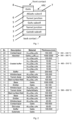
- Fig. 1 depicts a cross-section diagram of an example of multijunction photovoltaic device obtainable according to the method of the invention.
- the multijunction photovoltaic device is a complete solar cell.
- the multijunction photovoltaic device comprises a back contact (1), a bottom subcell (2) being GaAsBi subcell, a first tunnel junction (3), a middle subcell (4), a second tunnel junction (5), a top subcell (6), an antireflection coating (7), a front contact (8).
- the front contact (8) is formed in the shape of a grid, and the shape can vary and is optimized according to the device's requirements.
- the top subcell (6) is made of alloy, such as AlGaAs, with a bandgap energy in the range 1.82 -1.91 eV.
- the middle subcell (4) is made of alloy, such as GaAs, with a bandgap energy of 1.42 eV and is lattice matched to the top subcell (6).
- the bottom subcell (2) is made of GaAsBi alloy having larger lattice constant than the top two subcells and a bandgap energy of 1.0 eV.
- the subcells (2, 4, 6) are interconnected by tunnelling junctions (3, 5), which can themselves be made of GaAs and AlGaAs alloys.
- the middle subcell (4) a growth substrate, such as GaAs, can be removed from the photovoltaic device making the photovoltaic device a thin film device.
- the device can have any number of subcells, not necessarily three, as long as the GaAsBi subcell is the last subcell. If subcells are to be incorporated in the multijunction photovoltaic device above the GaAsBi subcell (2), the deposition of the further layers, or other processing steps of the device, for example, bonding, must not exceed 80 °C above the growth temperature of the GaAsBi alloy of the GaAsBi subcell.
- the multijunction photovoltaic device may comprise other standard collar cell elements to function as a solar cell and be handled with ease.
- Fig. 2 shows another example of a triple junction photovoltaic device obtainable according to the method of the invention.
- the triple junction photovoltaic device as shown in Fig. 2 is essentially the same as depicted in Fig. 1 but comprising initially grown semiconductor layers, including the growth substrate GaAs, still intact as they are after the device would have completed its growth process.
- the layer thicknesses are in a range to optimize the device efficiency under standard operating conditions. However, there are no restrictions on the layer thicknesses up to layer labelled Nr. 22.
- the contact layer labelled Nr. 22 growth time should not exceed 1 hour, if its growth temperature is more than 80 °C larger than the growth temperature of GaAsBi alloy. Thus, growth rate and layer thickness need to be optimized accordingly.
- the photovoltaic device of the second example comprises a semi-insulating GaAs substrate, labelled Nr. 0; a GaAs buffer layer, labelled Nr. 1; an etch-stop layer, labelled Nr. 2, which is used to assist with device processing if the GaAs substrate is chosen to be etched away afterward rather than being lifted-off. There can be more or fewer than two first layers after the GaAs substrate and can be chosen based on the subsequent substrate processing requirements.
- the photovoltaic device as shown in Fig. 2 also comprises GaAs contact layer, labelled Nr. 3; an AlGaAs window layer, labelled Nr. 4; a p-n diode comprised of emitter labelled Nr.
- the layers labelled Nr. 4 to 7 comprise the top AIGaAs subcell (6) as in the example of the triple junction solar cell as shown in Fig. 1 .
- the first tunnel diode labelled Nr. 8 is comprised of two highly doped thin layers (not shown in the diagram) comprising p-n diode with opposite polarity than the p-n diodes comprising the subcells.
- the tunnel diode can be made of two GaAs layers, or AlGaAs and GaAs.
- the following layers labelled Nr. 9 to 12 comprise the middle GaAs subcell (4) as in the example of the triple junction solar cell as shown in Fig. 1 .
- the second tunnel diode labelled Nr. 13 can be made the same way as the first tunnel diode described above.
- the following layers labelled Nr. 14 to 22 comprise the bottom GaAsBi subcell (2) as in the example of the triple junction solar cell as shown in Fig. 1 .
- a GaAs buffer layer labelled Nr. 15 is followed by compositionally graded InGaAs buffer labelled Nr. 16 to 20.
- the buffer layer is made with increasing content of In, which causes the crystal lattice constant to expand. In this process, dislocations are generated, but they mostly remain confined within the graded buffer layer.
- the final InGaAs buffer layer has slightly lower In content than the one below. It is also thicker to make the growth surface more even for the deposition of GaAsBi alloy.
- the buffer layer labelled Nr. 16 to 20 does not have to be necessarily InGaAs.
- GaAsBi alloy absorber layer labelled Nr. 21 can be either doped p- or n-type or left undoped. In the latter case, and as is proposed in this device, it would have an intrinsic (i) carrier concentration, which is typically slightly p-type.
- the semiconductor device growth is finalized with the InGaAs contact layer labelled Nr. 22. Layers labelled Nr. 20 to 22 comprise a p-i-n diode, since GaAsBi is left undoped.
- the InGaAs contact layer labelled Nr. 22 growth temperature is reduced, compared to the graded buffer InGaAs layers labelled Nr. 16 to 20, such that it is no higher than 80 °C above GaAsBi growth temperature.
- the reduction of InGaAs growth temperature by the proposed amount does not deteriorate its crystal quality, nor has other detrimental effects on its ability to act as a low resistivity contact layer with a metal that is deposited on top.
- the InGaAs contact layer is preferably highly doped, on the order of 1e19 cm -3 if p-type, or at least 8e18 cm -3 if it is n-type.
- In concentration of the InGaAs contact layer labelled Nr. 22, which is 8% here, is adjusted to obtain lattice matching with the underlying GaAsBi, by considering the lattice relaxation of the GaAsBi layer.
- Typical growth temperatures of: AIGaAs and GaAs subcells is 580 - 630 °C, graded InGaAs buffer is 480 - 510 °C, and GaAsBi is 300 - 350 °C.
- the indicated GaAsBi growth temperatures refer to GaAsBi with Bi content such that a 1.0 eV bandgap can be achieved with good material quality.
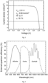
- Fig. 3 Current density-voltage measurements of the triple junction photovoltaic device according to the invention is shown in Fig. 3 .
- the bottom subcell (2) GaAsBi absorber thickness in the first example was 1200 nm.
- the measurements were conducted at room temperature by illuminating a completed mesa structure device with a total area of 0.2 cm 2 using an AM1.5G solar spectrum simulator.
- a double layer TiO 2 /SiO 2 antireflective coating was deposited on the completed device after etching the GaAs contact layer.
- the GaAs substrate was removed by etching.
- the photovoltaic device efficiency ( ⁇ ) was measured to be 19.1 %, open-circuit voltage (V oc ) 2.51 V, short-circuit current density (J sc ) 9.86 mA/cm 2 , and fill-factor (FF) 0.77. This demonstrates that a highly functional triple junction solar containing GaAsBi alloy is manufactured.
- EQE External quantum efficiency measurement of the triple junction photovoltaic device according to the invention is shown in Fig. 4 .
- the bottom GaAsBi subcell (2) shows spectral response down to 1250 nm wavelength, indicating its bandgap is 0.99 eV, close to the target bandgap of 1.0 eV.
- the bandgap combination of the triple junction device is 1.87 / 1.42 / 0.99 eV.
- the interference effects in GaAsBi EQE appear due to the incident light in the infrared portion of the spectrum that is not fully absorbed in the first pass through the GaAsBi absorber and being reflected from the back contact interfering within the device with the light field.
- the present method can be applied to other optoelectronic devices, such as but not limited to solid-state lasers, diodes, and sensors, that require a high-quality GaAsBi layer.
Landscapes
- Photovoltaic Devices (AREA)
Priority Applications (1)
| Application Number | Priority Date | Filing Date | Title |
|---|---|---|---|
| EP23171311.6A EP4459682A1 (de) | 2023-05-03 | 2023-05-03 | Verfahren zur herstellung einer photovoltaischen vorrichtung mit mehreren übergängen, die eine gaasbi unterzelle umfasst |
Applications Claiming Priority (1)
| Application Number | Priority Date | Filing Date | Title |
|---|---|---|---|
| EP23171311.6A EP4459682A1 (de) | 2023-05-03 | 2023-05-03 | Verfahren zur herstellung einer photovoltaischen vorrichtung mit mehreren übergängen, die eine gaasbi unterzelle umfasst |
Publications (1)
| Publication Number | Publication Date |
|---|---|
| EP4459682A1 true EP4459682A1 (de) | 2024-11-06 |
Family
ID=86328843
Family Applications (1)
| Application Number | Title | Priority Date | Filing Date |
|---|---|---|---|
| EP23171311.6A Pending EP4459682A1 (de) | 2023-05-03 | 2023-05-03 | Verfahren zur herstellung einer photovoltaischen vorrichtung mit mehreren übergängen, die eine gaasbi unterzelle umfasst |
Country Status (1)
| Country | Link |
|---|---|
| EP (1) | EP4459682A1 (de) |
Citations (3)
| Publication number | Priority date | Publication date | Assignee | Title |
|---|---|---|---|---|
| US7633083B2 (en) | 2004-03-10 | 2009-12-15 | Stc.Unm | Metamorphic buffer on small lattice constant substrates |
| US8697481B2 (en) | 2011-11-15 | 2014-04-15 | Solar Junction Corporation | High efficiency multijunction solar cells |
| US20140326301A1 (en) | 2011-08-29 | 2014-11-06 | Iqe Plc. | Multijunction photovoltaic device having sige(sn) and (in)gaasnbi cells |
-
2023
- 2023-05-03 EP EP23171311.6A patent/EP4459682A1/de active Pending
Patent Citations (3)
| Publication number | Priority date | Publication date | Assignee | Title |
|---|---|---|---|---|
| US7633083B2 (en) | 2004-03-10 | 2009-12-15 | Stc.Unm | Metamorphic buffer on small lattice constant substrates |
| US20140326301A1 (en) | 2011-08-29 | 2014-11-06 | Iqe Plc. | Multijunction photovoltaic device having sige(sn) and (in)gaasnbi cells |
| US8697481B2 (en) | 2011-11-15 | 2014-04-15 | Solar Junction Corporation | High efficiency multijunction solar cells |
Non-Patent Citations (10)
| Title |
|---|
| H. KAWATAS. HASEGAWAH. NISHINAKAM. YOSHIMOTO: "Improving the photovoltaic properties of GaAs/GaAsBi pin diodes by inserting a compositionally graded layer at the hetero-interface", SEMICOND. SCI. TECHNOL., vol. 37, 2022, pages 065016, Retrieved from the Internet <URL:https://doi.org/10.1088/1361-6641/ac66fa> |
| J. THOMAS ET AL.: "Requirements for a GaAsBi 1 eV sub-cell in a GaAs-based multi-junction solar cell", SEMICOND. SCI. TECHNOL., vol. 30, 2015, pages 094010, Retrieved from the Internet <URL:https://doi.org/10.1088/0268-1242/30/9/094010> |
| KHANOM SHAMIMA ET AL: "Simulation study of multijunction solar cell incorporating GaAsBi", 2017 IEEE REGION 10 HUMANITARIAN TECHNOLOGY CONFERENCE (R10-HTC), IEEE, 21 December 2017 (2017-12-21), pages 432 - 435, XP033320118, DOI: 10.1109/R10-HTC.2017.8288992 * |
| PAULAUSKAS T ET AL: "Epitaxial growth of GaAsBi on thin step-graded InGaAs buffer layers", SEMICONDUCTOR SCIENCE TECHNOLOGY, IOP PUBLISHING LTD, GB, vol. 37, no. 6, 19 April 2022 (2022-04-19), XP020420838, ISSN: 0268-1242, [retrieved on 20220419], DOI: 10.1088/1361-6641/AC61FF * |
| PAULAUSKAS, T.PACEBUTAS, V.GEIZUTIS, A. ET AL.: "GaAs1-xBix growth on Ge: anti-phase domains, ordering, and exciton localization", SCI REP, vol. 10, 2020, pages 2002, Retrieved from the Internet <URL:https://doi.org/10.1038/s41598-020-58812-y> |
| R. M. FRANCEJOHN F. GEISZTAO SONGWALDO OLAVARRIAMICHELLE YOUNGALAN KIBBLERMYLES A. STEINER: "Triple-junction solar cells with 39.5% terrestrial and 34.2% space efficiency enabled by thick quantum well superlattices", JOULE, vol. 6, no. 5, 2022, pages 1121 - 1135, Retrieved from the Internet <URL:https://doi.org/10.1016/j.joule.2022.04.024> |
| S. HASEGAWAK. KAKUYAMAH. NISHINAKAM. YOSHIMOTO: "PEDOT:PSS/GaAs1-xBix organic-inorganic solar cells", JAPANESE JOURNAL OF APPLIED PHYSICS, vol. 58, 2019, pages 060907, Retrieved from the Internet <URL:https://doi.org/10.7567/1347-4065/ab1e97> |
| SAKIB SYED NAZMUS ET AL: "Comparison of theoretical efficiencies of three and four layer multijunction solar cell and the effects of varying the bottom layer material", 2016 5TH INTERNATIONAL CONFERENCE ON INFORMATICS, ELECTRONICS AND VISION (ICIEV), IEEE, 13 May 2016 (2016-05-13), pages 995 - 1000, XP033012662, DOI: 10.1109/ICIEV.2016.7760148 * |
| SWEENEY STEPHEN JOHN ET AL: "The potential of GaAsBiN for multi-junction solar cells", 2013 IEEE 39TH PHOTOVOLTAIC SPECIALISTS CONFERENCE (PVSC), IEEE, 16 June 2013 (2013-06-16), pages 2474 - 2478, XP032568294, DOI: 10.1109/PVSC.2013.6744977 * |
| T PAULAUSKAS ET AL.: "Epitaxial growth of GaAsBi on thin step-graded InGaAs buffer layers", SEMICOND. SCI. TECHNOL., vol. 37, 2022, pages 065004, XP020420838, Retrieved from the Internet <URL:https://doi.org/10.1088/1361-6641/ac61ff> DOI: 10.1088/1361-6641/ac61ff |
Similar Documents
| Publication | Publication Date | Title |
|---|---|---|
| US7626116B2 (en) | Isoelectronic surfactant suppression of threading dislocations in metamorphic epitaxial layers | |
| JP5425480B2 (ja) | 倒置型メタモルフィック多接合ソーラーセルにおけるヘテロ接合サブセル | |
| Mauk et al. | GaSb-related materials for TPV cells | |
| US6252287B1 (en) | InGaAsN/GaAs heterojunction for multi-junction solar cells | |
| US7741146B2 (en) | Demounting of inverted metamorphic multijunction solar cells | |
| US7812249B2 (en) | Multijunction photovoltaic cell grown on high-miscut-angle substrate | |
| US5407491A (en) | Tandem solar cell with improved tunnel junction | |
| EP2641275B1 (de) | Typ-ii-tunnelübergänge mit hoher bandlücke einer inp-gitterkonstante für mehrfachsolarzellen | |
| US20090288703A1 (en) | Wide Band Gap Window Layers In Inverted Metamorphic Multijunction Solar Cells | |
| US20170054048A1 (en) | Four junction solar cell for space applications | |
| US20200251604A1 (en) | Distributed bragg reflector structures in multijunction solar cells | |
| JP2004296658A (ja) | 多接合太陽電池およびその電流整合方法 | |
| CN106549069B (zh) | 用于半导体器件的锑化物-基高带隙隧道结 | |
| US20150034152A1 (en) | Solar cell with passivation on the window layer | |
| EP4459682A1 (de) | Verfahren zur herstellung einer photovoltaischen vorrichtung mit mehreren übergängen, die eine gaasbi unterzelle umfasst | |
| Raman et al. | Multi‐Quantum Well‐Based Solar Cell | |
| EP3091583B1 (de) | Invertierte metamorphe solarzelle mit mehreren übergängen | |
| US20170365732A1 (en) | Dilute nitride bismide semiconductor alloys | |
| Mumtaz et al. | GaAsSbN for Multi-Junction Solar Cells | |
| US20150059837A1 (en) | Solar cell with passivation on the contact layer | |
| Wanlass et al. | Monolithic, series-connected InP/Ga/sub 0.47/In/sub 0.53/As tandem solar cells | |
| US20150040972A1 (en) | Inverted metamorphic multijunction solar cell with surface passivation of the contact layer | |
| Levillayer et al. | Development of 1 eV InGaAsN PIN subcell for MJSC integration and space application | |
| US11563133B1 (en) | Method of fabricating multijunction solar cells for space applications | |
| EP3171413A1 (de) | Invertierte metamorphische mehrfachsolarzelle |
Legal Events
| Date | Code | Title | Description |
|---|---|---|---|
| PUAI | Public reference made under article 153(3) epc to a published international application that has entered the european phase |
Free format text: ORIGINAL CODE: 0009012 |
|
| STAA | Information on the status of an ep patent application or granted ep patent |
Free format text: STATUS: REQUEST FOR EXAMINATION WAS MADE |
|
| 17P | Request for examination filed |
Effective date: 20240326 |
|
| AK | Designated contracting states |
Kind code of ref document: A1 Designated state(s): AL AT BE BG CH CY CZ DE DK EE ES FI FR GB GR HR HU IE IS IT LI LT LU LV MC ME MK MT NL NO PL PT RO RS SE SI SK SM TR |