EP4459677A1 - Schutzvorrichtung gegen elektrostatische entladungen - Google Patents
Schutzvorrichtung gegen elektrostatische entladungen Download PDFInfo
- Publication number
- EP4459677A1 EP4459677A1 EP24172073.9A EP24172073A EP4459677A1 EP 4459677 A1 EP4459677 A1 EP 4459677A1 EP 24172073 A EP24172073 A EP 24172073A EP 4459677 A1 EP4459677 A1 EP 4459677A1
- Authority
- EP
- European Patent Office
- Prior art keywords
- terminal
- diode
- node
- voltage
- anode
- Prior art date
- Legal status (The legal status is an assumption and is not a legal conclusion. Google has not performed a legal analysis and makes no representation as to the accuracy of the status listed.)
- Granted
Links
Images


Classifications
-
- H—ELECTRICITY
- H02—GENERATION; CONVERSION OR DISTRIBUTION OF ELECTRIC POWER
- H02H—EMERGENCY PROTECTIVE CIRCUIT ARRANGEMENTS
- H02H9/00—Emergency protective circuit arrangements for limiting excess current or voltage without disconnection
- H02H9/04—Emergency protective circuit arrangements for limiting excess current or voltage without disconnection responsive to excess voltage
- H02H9/045—Emergency protective circuit arrangements for limiting excess current or voltage without disconnection responsive to excess voltage adapted to a particular application and not provided for elsewhere
- H02H9/046—Emergency protective circuit arrangements for limiting excess current or voltage without disconnection responsive to excess voltage adapted to a particular application and not provided for elsewhere responsive to excess voltage appearing at terminals of integrated circuits
-
- H—ELECTRICITY
- H10—SEMICONDUCTOR DEVICES; ELECTRIC SOLID-STATE DEVICES NOT OTHERWISE PROVIDED FOR
- H10D—INORGANIC ELECTRIC SEMICONDUCTOR DEVICES
- H10D89/00—Aspects of integrated devices not covered by groups H10D84/00 - H10D88/00
- H10D89/60—Integrated devices comprising arrangements for electrical or thermal protection, e.g. protection circuits against electrostatic discharge [ESD]
- H10D89/601—Integrated devices comprising arrangements for electrical or thermal protection, e.g. protection circuits against electrostatic discharge [ESD] for devices having insulated gate electrodes, e.g. for IGFETs or IGBTs
- H10D89/711—Integrated devices comprising arrangements for electrical or thermal protection, e.g. protection circuits against electrostatic discharge [ESD] for devices having insulated gate electrodes, e.g. for IGFETs or IGBTs using bipolar transistors as protective elements
- H10D89/713—Integrated devices comprising arrangements for electrical or thermal protection, e.g. protection circuits against electrostatic discharge [ESD] for devices having insulated gate electrodes, e.g. for IGFETs or IGBTs using bipolar transistors as protective elements including a PNP transistor and a NPN transistor, wherein each of said transistors has its base region coupled to the collector region of the other transistor, e.g. silicon controlled rectifier [SCR] devices
-
- H—ELECTRICITY
- H10—SEMICONDUCTOR DEVICES; ELECTRIC SOLID-STATE DEVICES NOT OTHERWISE PROVIDED FOR
- H10D—INORGANIC ELECTRIC SEMICONDUCTOR DEVICES
- H10D89/00—Aspects of integrated devices not covered by groups H10D84/00 - H10D88/00
- H10D89/60—Integrated devices comprising arrangements for electrical or thermal protection, e.g. protection circuits against electrostatic discharge [ESD]
- H10D89/601—Integrated devices comprising arrangements for electrical or thermal protection, e.g. protection circuits against electrostatic discharge [ESD] for devices having insulated gate electrodes, e.g. for IGFETs or IGBTs
- H10D89/611—Integrated devices comprising arrangements for electrical or thermal protection, e.g. protection circuits against electrostatic discharge [ESD] for devices having insulated gate electrodes, e.g. for IGFETs or IGBTs using diodes as protective elements
Definitions
- This description relates generally to electronic devices, and more particularly to devices for protection against electrostatic discharges.
- Electrostatic discharges can produce, in integrated circuits or electronic components that are subjected to them, deleterious effects likely to cause irreversible deterioration of all or part of their constituent elements.
- An integrated circuit or an electronic component can thus suffer from significant malfunctions, or even be rendered completely inoperable, following an electrostatic discharge. If necessary, a replacement of the defective circuit or component may prove necessary, thus harming the reliability of electronic devices incorporating such circuits or components.
- integrated circuits and electronic components may include protective devices.
- existing protective devices against electrostatic discharges suffer from various drawbacks.
- existing devices are poorly suited to applications in which they are supposed to both protect, against electrostatic discharges, a component or circuit polarized by a voltage of the order of a few volts in nominal operation, and withstand, in the event of a short circuit, a voltage much higher than their nominal polarization voltage, for example a direct voltage of the order of several tens of volts.
- the first and second rectifying elements are diodes.
- the first and second rectifying elements each comprise a thyristor and a diode connecting an anode gate of the thyristor to a cathode of the thyristor.
- the capacitive element is a capacitor.
- the second terminal is a terminal for applying a reference potential.
- the device comprises at least two branches each comprising a single first rectification element, a single second diode and a single first terminal distinct from the first rectification elements, the second rectification elements and the first terminals of the other branches.
- one of the first terminals is connected to a third terminal for applying a reference potential.
- said at least one Zener diode or at least one Shockley diode is a single Zener diode.
- said Zener diode comprises an anode connected to a third node and a cathode connected to the first node, the capacitive element comprising a first terminal connected to the third node and a second terminal connected to the second node.
- said Zener diode comprises an anode connected to the second node and a cathode connected to a third node, the capacitive element comprising a first terminal connected to the third node and a second terminal connected to the first node.
- said at least one Zener diode or at least one Shockley diode is a single Shockley diode.
- said at least one Zener diode or at least one Shockley diode comprises at least two Zener diodes or at least two Shockley diodes.
- the first and second terminals are intended to be connected to terminals of a connector, for example a USB Type-C connector.
- One embodiment provides an electronic device, preferably a smartphone, connected object, touch pad or USB Type-C cable, comprising at least one device for protection against electrostatic discharges as described.
- the expressions “approximately”, “approximately”, “substantially”, and “of the order of” mean to within 10%, preferably to within 5%.
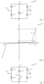
- FIG. 1 is an electrical diagram illustrating an example of a standard device 100 for protection against electrostatic discharges.
- the device 100 comprises four diodes 101, 103, 105 and 107. More precisely, in the example illustrated in figure 1 , the diode 101 comprises an anode electrode or terminal connected to a terminal 109 and a cathode electrode or terminal connected to an internal node 111 of the device 100. In this example, the diode 103 comprises an anode electrode or terminal connected to another internal node 113 of the device 100, distinct from the internal node 111, and a cathode electrode or terminal connected to the terminal 109.
- the diode 105 comprises an anode electrode or terminal connected to another terminal 115, distinct from the terminal 109, and a cathode electrode or terminal connected to the internal node 111
- the diode 107 comprises an anode electrode or terminal connected to the internal node 113 and a cathode electrode or terminal connected to the terminal 115.
- the diodes 101, 103, 105 and 107 of the device 100 are for example identical to each other, apart from manufacturing dispersions.
- each diode 101, 103, 105, 107 has a breakdown voltage of the order of 22 V.
- Terminal 109 is for example intended to be connected to an input terminal, an output terminal or an input-output terminal of a connector, an integrated circuit or an electronic component to be protected against electrostatic discharges.
- Terminal 109 is for example adapted to be connected to a terminal for receiving and/or transmitting a digital or analog signal. In nominal operation, terminal 109 is for example subjected to a voltage less than or equal to 5 V.
- terminal 109 is intended to be connected to a communication terminal or pin "SBU1", “SBU2", “CC1" or "CC2" of a plug or socket of a USB Type-C (USB-C) connector.
- the plug or socket is for example part of a cable or an electronic device, for example a mobile phone, a smartphone, a connected object, a touch pad, etc.
- Terminal 115 is for example a terminal for applying a reference potential, for example ground.
- a reference potential for example ground.
- terminal 115 is intended to be connected to a ground “GND” terminal or pin of the plug or socket.
- the electrostatic discharge protection device 100 further comprises a diode 117, for example a Zener diode, connecting the internal node 111 to the internal node 113. More precisely, in the example illustrated in figure 1 , diode 117 includes an anode electrode or terminal connected to internal node 113 and a cathode electrode or terminal connected to internal node 111.
- diode 117 includes an anode electrode or terminal connected to internal node 113 and a cathode electrode or terminal connected to internal node 111.
- the diode 117 of the device 100 is for example dimensioned so that it is in a blocked state, i.e. non-conductive, when the terminal 109 is subjected to its nominal operating voltage. Furthermore, the diode 117 is dimensioned so that it is in the blocked state in the event of a short circuit.
- a short circuit may for example occur between the terminal or pin to which the terminal 109 is connected and a “Vbus” power supply terminal or pin adjacent to this terminal.
- the diode 117 has for example a reverse voltage threshold equal to approximately 22 V.
- the diodes 101, 103, 105 and 107 have a strictly lower capacitance, for example at least ten times lower, than that of the diode 117. This makes it possible to “mask” the capacitance of the diode 117, thus avoiding disturbing the signals present on the terminal 109.
- the current-voltage characteristic of the figure 2 more precisely comprises a curve 201 illustrating variations in intensity (I) of a current flowing through the device 100 as a function of a bias voltage (V) applied between the terminals 109 and 115.
- the curve 201 comprises left and right parts corresponding respectively to the case where the voltage V is negative and to the case where the voltage V is positive.
- the left and right parts of the curve 201 are for example substantially identical, apart from the sign. For simplicity, only the right part of the curve 201 will be detailed below, the transposition of the description on the left part of curve 201 being within the reach of the person skilled in the art from the indications below.
- the bias voltage V can for example take values between 0 V and a limit voltage V WM .
- the limit voltage V WM corresponds for example to a maximum voltage value V intended for a given application.
- the limit voltage V WM is for example of the order of 20 V, in a case where the terminal 109 of the device 100 is intended to be connected to a communication terminal “SBU1”, “SBU2”, “CC1” or “CC2” forming part of a USB Type-C connector and where the voltage applied to the “Vbus” terminals of the connector, likely to form a short circuit with the terminal 109, is equal to approximately 20 V.
- the device 100 is biased under this limit voltage V WM , it is traversed by a low leakage current I L .
- the bias voltage V may temporarily exceed a threshold voltage V tr .
- the threshold voltage V tr corresponds here to a trigger voltage of the protection.
- the device 100 in particular the diode 117, is dimensioned so that the threshold voltage V tr is greater than the limit voltage V WM provided for in the application considered.
- the threshold voltage V tr In a case where the threshold voltage V tr is exceeded, that is to say once the protection has been triggered for example due to an electrostatic discharge applying, between terminals 109 and 115, a voltage V greater than V tr , the voltage V drops slightly to a holding voltage value V h .
- the holding voltage V h corresponds to the voltage Minimum V that can be reached after the protection has been triggered.
- a current I t greater than the leakage current I L flows through diode 117.
- the electrostatic discharge may nevertheless be sufficiently large so that the bias voltage V of the device 100 continues to increase even after the protection has been triggered.
- This increase in voltage V is accompanied by an increase in the current I flowing through the diode 117.
- the value of the polarization voltage V can then increase up to a value V cl called the blocking voltage (“clamping voltage” in English) or clipping voltage.
- V cl corresponds to a maximum current I PP acceptable by the protection (“peak pulse current” in English).
- a disadvantage of the device 100 is that, in order to allow electrostatic discharges to be discharged while being able to withstand short circuits, the diode 117 must have a trigger voltage V tr that is much higher, for example of the order of ten times higher, than the nominal voltage of the terminal 109 in the absence of a short circuit. This is detrimental to the discharge of electrostatic discharges by the device 100, because the voltage applied between the terminals 109 and 115 in the event of an electrostatic discharge increases from a value of the holding voltage V h that is also of the order of ten times higher than the nominal voltage. As a result, the circuit(s) and/or component(s) protected by the device 100 may be subjected to high voltages V, for example of the order of 25 V, in case of electrostatic discharge, which may damage them.
- FIG. 3 is an electrical diagram illustrating an example of a device 300 for protection against electrostatic discharges according to one embodiment.
- Device 300 of the figure 3 includes elements in common with device 100 of the figure 1 . These common elements will not be detailed again below.
- Device 300 of the figure 3 differs from device 100 of the figure 1 in that the device 300 comprises a diode 301, for example a Zener diode, and a capacitive element 303 in series between the internal nodes 111 and 113.
- the diode 301 and the capacitive element 303 are connected in series between the node 111 and the node 113. More precisely, in the example illustrated in figure 3 , the diode 301 comprises an anode electrode or terminal connected to another internal node 305, distinct from the nodes 113 and 111, and a cathode electrode or terminal connected to the internal node 111.
- the capacitive element 303 comprises an electrode or terminal connected to the internal node 305 and another electrode or terminal connected to the internal node 113.
- the diode 301 of the device 300 is for example similar to the diode 117 of the device 100, but differs from the diode 117 in that it has a strictly lower trigger voltage, for example approximately four times lower, than that of the diode 117.
- the diode 301 has a trigger voltage or reverse voltage of the order of 5 V, in absolute value, in a case where the nominal voltage applied between the terminals 109 and 115 is less than or equal to 5 V, in absolute value.
- the figure 3 illustrates an example where diode 301 connects node 111 to node 305 and capacitive element 303 connects node 305 to node 113.
- the positions of the diode 301 and the capacitive element 303 in the device 300 may, as a variant, be interchanged, so that the diode 301 connects the node 305 to the node 113, the anode and the cathode of the diode 301 then being respectively connected to the nodes 113 and 305, and so that the capacitive element 303 connects the node 111 to the node 305.
- the capacitive element 303 of the device 300 is more precisely a capacitor comprising two electrically conductive electrodes or armatures, for example two metal electrodes parallel to each other, separated from each other by a dielectric material.
- the device 300 may be made in whole or in part from discrete components.
- the device 300 has for example a monolithic structure with the exception of the capacitive element 303, formed by a discrete component.
- the device 300 may have a fully monolithic structure, i.e. a structure whose elements are completely integrated, the capacitive element 303 then being, for example, a capacitor of the MIM type (from the English “Metal Insulator Metal”) formed in a stack of electrically conductive levels, for example metal layers, separated from each other by electrically insulating levels, for example dielectric layers.
- MIM Metal Insulator Metal
- the capacitive element 303 has a capacitance between 100 nF and 10 ⁇ F.
- the device 300 may further comprise a component or circuit for discharging the capacitive element 303, for example a resistor associated in parallel with the capacitive element 303.
- a means for discharging the capacitive element 303 of the device 300 may comprise a transistor, for example a MOS (metal-oxide-semiconductor) transistor, one conduction terminal of which, for example a drain electrode, is connected to the node 305, another conduction terminal of which, for example a source electrode, is connected to the terminal 113 and one control terminal of which, for example a gate electrode, is connected to a control circuit.
- MOS metal-oxide-semiconductor
- the current-voltage characteristic of the figure 4 more specifically comprises a curve 401 illustrating variations in intensity (I) of a current flowing through the device 300 as a function of a bias voltage (V) applied between the terminals 109 and 115 of the device 300.
- the curve 401 illustrates a “dynamic” operation of the device 300, i.e. when the device 300 is subjected to an electrostatic discharge, the capacitive element 303 then behaving like a short circuit, whereas, in “static” operation, i.e.
- the capacitive element 303 behaves like an open circuit and the current-voltage characteristic of the device 300 then has a different shape from that of the curve 401.
- the curve 401 comprises left and right parts corresponding respectively to the case where the voltage V is negative and to the case where the voltage V is positive.
- the left and right parts of curve 401 are for example substantially identical, apart from the sign. To simplify, only the right part of curve 401 will be detailed below, the transposition of the description on the left part of the curve 401 being within the reach of the person skilled in the art from the indications below.
- curve 201 was represented in figure 4 for comparison. Unlike curve 401 which illustrates only the dynamic operation of the device 300, curve 201 illustrates for example both the static operation and the dynamic operation of the device 100.
- Device 300 of the figure 3 has a threshold voltage V' tr strictly lower, for example at least two times lower, for example approximately five times lower, than the threshold voltage V tr of the device 100 of the figure 1 .
- This allows the device 300 to discharge electrostatic discharges more efficiently than the device 100, because the voltage V applied between the terminals 109 and 115 of the device 300 in the event of an electrostatic discharge increases from a lower value than in the case of the device 100, for example a value of the order of the nominal voltage applied to the terminal 109.
- the device 300 has a dynamic resistance R d lower than that of the device 100, which allows the device 300 to achieve higher performances in terms of discharging electrostatic discharges than the device 100, in particular a lower voltage V, for the same current value I.
- An advantage of the device 300 is therefore that it allows electrostatic discharges to be evacuated more effectively than the device 100, while remaining protected against short circuits.
- FIG. 5 is an electrical diagram illustrating another example of an electrostatic discharge protection device 500 according to one embodiment.
- the device 500 of the figure 5 includes common elements with the device 300 of the figure 3 . These common elements will not be detailed again below.
- the 500 device of the figure 5 differs from the 300 device of the figure 3 in that the device 500 comprises a turnaround diode 501, also called a Shockley diode, connecting the internal node 111 to the internal node 305.
- a turnaround diode 501 also called a Shockley diode
- the voltage V applied between the terminals 109 and 115 of the device 500 in the event of an electrostatic discharge increases from an even lower value than in the case of the device 300, for example a substantially zero value. This advantageously allows the device 500 to achieve performances in terms of protection against electrostatic discharges even higher than those of the device 300.
- the voltage V between terminals 109 and 115 of the device 500 is equal to approximately 13 V.
- FIG. 6 is an electrical diagram illustrating another example of an electrostatic discharge protection device 600 according to one embodiment.
- the device 600 of the figure 6 includes common elements with the 300 device of the figure 3 . These common elements will not be detailed again below.
- Device 600 of the figure 6 differs from the 300 device of the figure 3 in that the device 600 comprises several diodes 601 in series between the internal nodes 305 and 111. More precisely, in the example illustrated in figure 6 , the device 600 comprises three diodes 601-1, 601-2 and 601-3, for example Zener diodes, associated in series between the node 305 and the node 111.
- the diode 601-1 comprises an anode electrode or terminal connected to a cathode electrode or terminal of the diode 601-2, and a cathode electrode or terminal connected to the node 111.
- the diode 601-2 comprises an anode electrode or terminal connected to a cathode electrode or terminal of the diode 601-3
- the diode 601-3 comprises an anode electrode or terminal connected to the node 305.
- the figure 6 illustrates an example in which the device 600 comprises a group 603 of three diodes 601-1, 601-2 and 601-3, the group 603 can of course comprise any number, greater than or equal to two, of diodes connecting the node 305 to the node 111.
- each diode 601-1, 601-2, 601-3 is subjected, at its terminals, to a voltage substantially equal to one third of the voltage applied between the terminals of the diode 301 of the device 300.
- the voltage applied between the nodes 111 and 305 is distributed between the diodes 601-1, 601-2 and 601-3.
- FIG. 7 is an electrical diagram illustrating another example of an electrostatic discharge protection device 700 according to one embodiment.
- the device 700 of the figure 7 includes common elements with the device 300 of the figure 3 . These common elements will not be detailed again below.
- Device 700 of the figure 7 differs from the 300 device of the figure 3 in that the device 700 is devoid of diodes 105 and 107 and in that the device 700 comprises several terminals 109 (four terminals 109-1, 109-2, 109-3 and 109-4, in the illustrated example) each connected between two diodes 103 and 101 in series.
- One of the terminals 109 of the device 700 (terminal 109-4, in the illustrated example) is connected to the node 115 for applying the reference potential.
- the device 700 comprises several branches 701 (four branches 701, in the example shown) each comprising the terminal 109 (109-1, 109-2, 109-3 or 109-4) connected to the anode of the diode 101 (101-1, 101-2, 101-3 or 101-4) and to the cathode of the diode 103 (103-1, 103-2, 103-3 or 103-4), the anode of the diode 103 being connected to the internal node 113 and the cathode of the diode 101 being connected to the internal node 111.
- the figure 7 illustrates an example in which the device 700 comprises four branches 701, the device 700 may, alternatively, comprise any number, greater than or equal to two, of branches 701.
- the diode 101, the diode 103 and the terminal 109 of each branch 701 are distinct from diode 101, diode 103 and terminal 109 of the other branches 701 of device 700.
- terminals 109-1, 109-2, 109-3, and 109-4 are intended to be connected to separate terminals or pins of a USB Type-C connector.
- the device 700 has an operation and advantages similar to those of the device 300 of the figure 3 .
- An additional advantage of the device 700 is that the device 700 allows the diode 301 and the capacitive element 303 to be shared for several terminals 109. This thus allows the device 700 to have a complexity, cost and size lower than those which would be obtained by using a device 300 for each terminal 109 (109-1, 109-2, 109-3 and 109-4) to be protected.
- FIG 8 is an electrical diagram illustrating another example of an electrostatic discharge protection device 800 according to one embodiment.
- the device 800 of the figure 8 includes common elements with the device 300 of the figure 3 . These common elements will not be detailed again below.
- the 800 device of the figure 8 differs from the 300 device of the figure 3 in that the rectifying elements, constituted by the diodes 101, 103, 105 and 107 in the case of the device 300, are, in the case of the device 800, substituted respectively by assemblies 801, 803, 805 and 807 each comprising a thyristor 809 and a diode 811.
- the thyristor 809 comprises an anode gate connected, by the diode 811, to a cathode electrode or terminal of the thyristor 809. More precisely, the diode 811 comprises an anode electrode or terminal connected to the anode gate of the thyristor 809, and a cathode electrode or terminal connected to the cathode electrode or terminal of the thyristor 809.
- Each assembly 801, 803, 805, 807 comprises an anode electrode or terminal corresponding to an anode electrode or terminal of the thyristor 809 and a cathode electrode or terminal corresponding to the cathode electrode or terminal of the thyristor 809.
- What has been described previously in relation to the anode and cathode electrodes or terminals of the diodes 101, 103, 105 and 107 of the device 300 of the figure 3 in particular the connections of these electrodes or terminals with the other terminals and nodes of the device 300, is transposable by the person skilled in the art to the anode and cathode electrodes or terminals of the assemblies 801, 803, 805 and 807, respectively, of the device 800 of the figure 8 .
- the embodiment of the device 800 could be combined with each of the embodiments of the devices 500, 600 and 700, each diode 101, 103, 105, 107 of these devices being able to be replaced by an assembly identical or similar to the assemblies 801, 803, 805 and 807, that is to say by a rectifier element comprising a thyristor 809 whose anode trigger is connected to its cathode electrode or terminal by a diode 811.
- bidirectional 300, 500, 600, 700 and 800 protection devices capable of discharging positive or negative overvoltages indifferently, have been described above in relation to the figures 3 , 5 , 6 , 7 and 8 , it would be possible, from the indications of the present description, to produce unidirectional protection devices, capable of evacuating only positive or negative overvoltages.
- Such devices can for example be obtained by connecting the terminal 115 for applying the reference potential to the node 113 rather than to the node 109 in each of the devices 300, 500, 600, 700 and 800.
- the person skilled in the art is furthermore capable of determining the values of the threshold voltages of the diodes 101, 103, 105, 107, 117, 301, 501, 601-1, 601-2 and 601-3 and the capacitance of the capacitive element 303 depending on the application, for example using digital simulation tools.
- terminals 109 and 115 correspond to terminals or pins of a USB Type-C connector
- the embodiments described are not limited to this application but can be implemented in any type of electronic device, component, circuit, etc. capable of being protected against electrostatic discharges and of undergoing short circuits.
- the positions of the capacitive element 303 on the one hand, and of the reversing diode 501, of the group 603 of diodes 601 or of the diode 301 on the other hand, can be interchanged in the protection devices 500, 600 and 700, respectively.
Landscapes
- Engineering & Computer Science (AREA)
- Microelectronics & Electronic Packaging (AREA)
- Emergency Protection Circuit Devices (AREA)
- Semiconductor Integrated Circuits (AREA)
Applications Claiming Priority (1)
| Application Number | Priority Date | Filing Date | Title |
|---|---|---|---|
| FR2304475A FR3148495A1 (fr) | 2023-05-04 | 2023-05-04 | Dispositif de protection contre des décharges électrostatiques |
Publications (2)
| Publication Number | Publication Date |
|---|---|
| EP4459677A1 true EP4459677A1 (de) | 2024-11-06 |
| EP4459677B1 EP4459677B1 (de) | 2026-03-11 |
Family
ID=87889515
Family Applications (1)
| Application Number | Title | Priority Date | Filing Date |
|---|---|---|---|
| EP24172073.9A Active EP4459677B1 (de) | 2023-05-04 | 2024-04-24 | Schutzvorrichtung gegen elektrostatische entladungen |
Country Status (3)
| Country | Link |
|---|---|
| US (1) | US20240372359A1 (de) |
| EP (1) | EP4459677B1 (de) |
| FR (1) | FR3148495A1 (de) |
Families Citing this family (1)
| Publication number | Priority date | Publication date | Assignee | Title |
|---|---|---|---|---|
| JP2024138854A (ja) * | 2023-03-27 | 2024-10-09 | 株式会社東芝 | 静電保護回路 |
Citations (4)
| Publication number | Priority date | Publication date | Assignee | Title |
|---|---|---|---|---|
| US20110212595A1 (en) * | 2010-02-26 | 2011-09-01 | Jerry Hu | Semiconductor device structure and methods of making |
| US20150207312A1 (en) * | 2014-01-17 | 2015-07-23 | Silergy Semiconductor Technology (Hangzhou) Ltd | Low Capacitance Transient Voltage Suppressor |
| US20170221875A1 (en) * | 2016-02-01 | 2017-08-03 | Ubiq Semiconductor Corp. | Diode device of transient voltage suppressor and manufacturing method thereof |
| WO2020115413A1 (fr) * | 2018-12-04 | 2020-06-11 | Legrand France | Variateur électronique pour circuit basse tension |
-
2023
- 2023-05-04 FR FR2304475A patent/FR3148495A1/fr active Pending
-
2024
- 2024-04-22 US US18/642,513 patent/US20240372359A1/en active Pending
- 2024-04-24 EP EP24172073.9A patent/EP4459677B1/de active Active
Patent Citations (4)
| Publication number | Priority date | Publication date | Assignee | Title |
|---|---|---|---|---|
| US20110212595A1 (en) * | 2010-02-26 | 2011-09-01 | Jerry Hu | Semiconductor device structure and methods of making |
| US20150207312A1 (en) * | 2014-01-17 | 2015-07-23 | Silergy Semiconductor Technology (Hangzhou) Ltd | Low Capacitance Transient Voltage Suppressor |
| US20170221875A1 (en) * | 2016-02-01 | 2017-08-03 | Ubiq Semiconductor Corp. | Diode device of transient voltage suppressor and manufacturing method thereof |
| WO2020115413A1 (fr) * | 2018-12-04 | 2020-06-11 | Legrand France | Variateur électronique pour circuit basse tension |
Also Published As
| Publication number | Publication date |
|---|---|
| FR3148495A1 (fr) | 2024-11-08 |
| EP4459677B1 (de) | 2026-03-11 |
| US20240372359A1 (en) | 2024-11-07 |
Similar Documents
| Publication | Publication Date | Title |
|---|---|---|
| EP0215707A1 (de) | Spannungsschaltvorrichtung | |
| WO2011089179A1 (fr) | Dispositif electronique, en particulier de protection contre les décharges électrostatistiques, et procédé de protection d'un composant contre des décharges électrostatiques | |
| FR2602620A1 (fr) | Circuit de commutation a semiconducteurs | |
| EP3096456A1 (de) | Bidirektioneller leistungsumschalter mit verbesserten umschaltleistungen | |
| EP2290691A1 (de) | Schutzvorrichtung für einen integrierten Schaltkreis gegen elektrostatische Entladungen | |
| EP0742591B1 (de) | Bauelement für den vollständigen Schutz einer Schnittstellenschaltung von Teilnehmerleitungen | |
| EP4459677B1 (de) | Schutzvorrichtung gegen elektrostatische entladungen | |
| EP3070798B1 (de) | Schutzvorrichtung gegen überspannungen | |
| EP3706274B1 (de) | Schutzvorrichtung gegen überspannungen | |
| FR2740924A1 (fr) | Protection d'entree pour un amplificateur a bande passante elevee | |
| EP3863140A1 (de) | Schutz gegen überspannungen | |
| FR2670340A1 (fr) | Circuit de protection a faible capacite. | |
| FR3049766A1 (fr) | Dispositif de protection contre des decharges electrostatiques a seuil de declenchement ajustable | |
| FR2715504A1 (fr) | Circuit intégré incorporant une protection contre les décharges électrostatiques. | |
| FR2572600A1 (fr) | Stabilisateur electronique de tension, utilisable en particulier dans l'automobile, avec protection contre les surtensions transitoires de polarite opposee a celle du generateur | |
| FR3106454A1 (fr) | Décharge de condensateur | |
| EP2348528A1 (de) | Schutzvorrichtung für einen integrierten Schaltkreis gegen elektrostatische Entladungen | |
| EP4432358B1 (de) | Schutzvorrichtung gegen elektrostatische entladungen | |
| FR2859858A1 (fr) | Circuit de protection d'entree video destine a etre connecte a un circuit video | |
| EP0895331B1 (de) | Schutzvorrichtung für elektrische Last und Versorgungseinrichtung mit einer solchen Vorrichtung | |
| FR3079348A1 (fr) | Circuit de protection contre les decharges electrostatiques | |
| EP3370256B1 (de) | Kompakte vorrichtung zum schutz eines integrierten schaltkreises gegen elektrostatische entladungen | |
| EP3568894A1 (de) | Vorrichtung zum schutz von elektrischer ausrüstung | |
| FR3119493A1 (fr) | Dispositif de protection contre les décharges électrostatiques | |
| FR2863786A1 (fr) | Equilibrage des tensions de generateurs electrochimiques de batterie rechargeable, par circuit a dipole(s) |
Legal Events
| Date | Code | Title | Description |
|---|---|---|---|
| PUAI | Public reference made under article 153(3) epc to a published international application that has entered the european phase |
Free format text: ORIGINAL CODE: 0009012 |
|
| STAA | Information on the status of an ep patent application or granted ep patent |
Free format text: STATUS: REQUEST FOR EXAMINATION WAS MADE |
|
| 17P | Request for examination filed |
Effective date: 20240424 |
|
| AK | Designated contracting states |
Kind code of ref document: A1 Designated state(s): AL AT BE BG CH CY CZ DE DK EE ES FI FR GB GR HR HU IE IS IT LI LT LU LV MC ME MK MT NL NO PL PT RO RS SE SI SK SM TR |
|
| REG | Reference to a national code |
Ref country code: DE Ref legal event code: R079 Free format text: PREVIOUS MAIN CLASS: H01L0027020000 Ipc: H10D0089600000 Ref country code: DE Ref legal event code: R079 Ref document number: 602024003066 Country of ref document: DE Free format text: PREVIOUS MAIN CLASS: H01L0027020000 Ipc: H10D0089600000 |
|
| GRAP | Despatch of communication of intention to grant a patent |
Free format text: ORIGINAL CODE: EPIDOSNIGR1 |
|
| STAA | Information on the status of an ep patent application or granted ep patent |
Free format text: STATUS: GRANT OF PATENT IS INTENDED |
|
| RIC1 | Information provided on ipc code assigned before grant |
Ipc: H10D 89/60 20250101AFI20251210BHEP Ipc: H02H 9/04 20060101ALI20251210BHEP |
|
| INTG | Intention to grant announced |
Effective date: 20251218 |
|
| GRAS | Grant fee paid |
Free format text: ORIGINAL CODE: EPIDOSNIGR3 |
|
| GRAA | (expected) grant |
Free format text: ORIGINAL CODE: 0009210 |
|
| STAA | Information on the status of an ep patent application or granted ep patent |
Free format text: STATUS: THE PATENT HAS BEEN GRANTED |
|
| AK | Designated contracting states |
Kind code of ref document: B1 Designated state(s): AL AT BE BG CH CY CZ DE DK EE ES FI FR GB GR HR HU IE IS IT LI LT LU LV MC ME MK MT NL NO PL PT RO RS SE SI SK SM TR |
|
| REG | Reference to a national code |
Ref country code: CH Ref legal event code: F10 Free format text: ST27 STATUS EVENT CODE: U-0-0-F10-F00 (AS PROVIDED BY THE NATIONAL OFFICE) Effective date: 20260311 Ref country code: GB Ref legal event code: FG4D Free format text: NOT ENGLISH |