EP4459512A2 - Layouts for fault-tolerant quantum computers - Google Patents
Layouts for fault-tolerant quantum computers Download PDFInfo
- Publication number
- EP4459512A2 EP4459512A2 EP24201171.6A EP24201171A EP4459512A2 EP 4459512 A2 EP4459512 A2 EP 4459512A2 EP 24201171 A EP24201171 A EP 24201171A EP 4459512 A2 EP4459512 A2 EP 4459512A2
- Authority
- EP
- European Patent Office
- Prior art keywords
- qubits
- qubit
- target
- ancilla
- quantum
- Prior art date
- Legal status (The legal status is an assumption and is not a legal conclusion. Google has not performed a legal analysis and makes no representation as to the accuracy of the status listed.)
- Pending
Links
Images







Classifications
-
- G—PHYSICS
- G06—COMPUTING OR CALCULATING; COUNTING
- G06N—COMPUTING ARRANGEMENTS BASED ON SPECIFIC COMPUTATIONAL MODELS
- G06N5/00—Computing arrangements using knowledge-based models
- G06N5/01—Dynamic search techniques; Heuristics; Dynamic trees; Branch-and-bound
-
- G—PHYSICS
- G06—COMPUTING OR CALCULATING; COUNTING
- G06F—ELECTRIC DIGITAL DATA PROCESSING
- G06F30/00—Computer-aided design [CAD]
- G06F30/30—Circuit design
- G06F30/39—Circuit design at the physical level
- G06F30/392—Floor-planning or layout, e.g. partitioning or placement
-
- G—PHYSICS
- G06—COMPUTING OR CALCULATING; COUNTING
- G06N—COMPUTING ARRANGEMENTS BASED ON SPECIFIC COMPUTATIONAL MODELS
- G06N10/00—Quantum computing, i.e. information processing based on quantum-mechanical phenomena
- G06N10/20—Models of quantum computing, e.g. quantum circuits or universal quantum computers
-
- G—PHYSICS
- G06—COMPUTING OR CALCULATING; COUNTING
- G06N—COMPUTING ARRANGEMENTS BASED ON SPECIFIC COMPUTATIONAL MODELS
- G06N10/00—Quantum computing, i.e. information processing based on quantum-mechanical phenomena
- G06N10/40—Physical realisations or architectures of quantum processors or components for manipulating qubits, e.g. qubit coupling or qubit control
-
- G—PHYSICS
- G06—COMPUTING OR CALCULATING; COUNTING
- G06N—COMPUTING ARRANGEMENTS BASED ON SPECIFIC COMPUTATIONAL MODELS
- G06N10/00—Quantum computing, i.e. information processing based on quantum-mechanical phenomena
- G06N10/70—Quantum error correction, detection or prevention, e.g. surface codes or magic state distillation
-
- H—ELECTRICITY
- H03—ELECTRONIC CIRCUITRY
- H03K—PULSE TECHNIQUE
- H03K19/00—Logic circuits, i.e. having at least two inputs acting on one output; Inverting circuits
- H03K19/20—Logic circuits, i.e. having at least two inputs acting on one output; Inverting circuits characterised by logic function, e.g. AND, OR, NOR, NOT circuits
-
- G—PHYSICS
- G06—COMPUTING OR CALCULATING; COUNTING
- G06N—COMPUTING ARRANGEMENTS BASED ON SPECIFIC COMPUTATIONAL MODELS
- G06N5/00—Computing arrangements using knowledge-based models
- G06N5/02—Knowledge representation; Symbolic representation
- G06N5/022—Knowledge engineering; Knowledge acquisition
Definitions
- Disclosed herein are example layouts and layout generation techniques for fault-tolerant quantum computers.
- the particular embodiments described should not be construed as limiting, as the disclosed method acts can be performed alone, in different orders, or at least partially simultaneously with one another. Further, any of the disclosed methods or method acts can be performed with any other methods or method acts disclosed herein. Likewise, the disclosed combinations of features can include rearrangements of any novel or nonobvious combination or subcombination of features.
- One example embodiment comprises a method for performing a layout reduction technique for fault-tolerant quantum computing.
- the method is performed by one or more classical computing devices, at least some of which are in a configuration that can operate a quantum computer.
- a layout of an arbitrary quantum circuit is reduced to a layout of exponents of a multiple qubit Pauli matrix and measurements of a multiple qubit Pauli matrix; and a quantum computer is configured to implement the reduced layout.
- qubits of the quantum computer comprise data qubits, interface qubits, and ancilla qubits.
- a graph of qubit connectivity satisfies a condition of providing an ancilla-path from one or more data qubits to the interface qubits.
- Another example embodiment comprises another method for performing a layout technique for fault-tolerant quantum computing.
- the method is performed by one or more classical computing devices, at least some of which are in a configuration that can operate a quantum computer.
- qubits are marked as one of a data, interface, or ancilla qubit for a 2D nearest neighbor graph of qubit connectivity; an ancilla-path is provided from a respective data qubit to a respective interface qubit; and a quantum computer is configured to implement the ancilla-path from a respective data qubit to a respective interface qubit.
- the method accounts for and avoids any broken qubits and satisfies a condition of providing an ancilla-path from a data qubit to the interface qubits.
- any of the methods described above can be performed in a system, comprising a quantum computing device; and one or more classical-computing devices, at least some of the one or more classical computing devices being programmed to perform any of the disclosed methods.
- any of the methods described above can be implemented as one or more classical-computer-readable-media storing classical-computer-executable instructions, which when executed by a classical computer cause the classical computer to perform any of the disclosed methods.
- a quantum circuit configured to apply an exponent of a multiple qubit Pauli matrix and measure a multiple qubit Pauli matrix.
- an ancilla-path is provided from data qubits to the interface qubits.
- the quantum circuit has a depth not depending on the number of vertexes.
- the quantum circuit uses single or low-depth multiple-target CNOT gates as a sub-circuits.
- Some embodiments comprise a quantum circuit configured to (a) provide a multi-target CNOT gate using a single-qubit and two-qubit Pauli measurements and single qubit Clifford gates; or (b) provide a multi-target CNOT gate using a single-qubit, Pauli measurements, single qubit Clifford gates and Controlled-Z gates.
- the quantum circuit provides a multi-target CNOT gate using a single-qubit and two-qubit Pauli measurements and single qubit Clifford gates, wherein the quantum circuit works with qubits for which a graph of qubit connectivity satisfies a condition of providing an ancilla-path from a target qubit to the control qubit.
- the quantum circuit provides a multi-target CNOT gate using a single-qubit and two-qubit Pauli measurements and single qubit Clifford gates, wherein the quantum circuit has a depth not depending on the number of vertexes.
- the quantum circuit is configured to provide a multi-target CNOT gate using a single-qubit, Pauli measurements, single qubit Clifford gates and Controlled-Z gates, and wherein the quantum circuit works with qubits for which graph of qubit connectivity satisfies a condition of providing an ancilla-path from a target qubit to the control qubit.
- the quantum circuit is configured to provide a multi-target CNOT gate using a single-qubit, Pauli measurements, single qubit Clifford gates and Controlled-Z gates, wherein the quantum circuit has a depth not depending on the number of vertexes.
- I, X, Y and Z denote single qubit Pauli matrices. All single qubit Pauli matrices are Hermitian matrices. Square of every Pauli matrix is equal to I.
- a multiple qubit Pauli matrix is a tensor product (denoted as ⁇ ) of single qubit Pauli matrices.
- Notation X k , Y k , Z k refers to a multiple qubit Pauli matrix with X, Y and Z on qubit k and I on all other qubits.
- X 2 as 3 qubit Pauli matrix refers to the matrix: I ⁇ X ⁇ I .
- Multiple qubit Pauli matrices are also Hermitian and their square is the identity matrix. Below, the multiple qubit Pauli matrix will simply be called a Pauli matrix. I is used for the identity matrix on any number of qubits. The dimension of I will be clear from the context.
- k is used for the k -th component of the multi-qubit Pauli matrix.
- P X a Y b Z c
- a X
- b Y
- c Z.
- Tr( A ) is the sum of the diagonal elements of A.
- Tr(AB) Tr(BA).
- Tr( A ⁇ B ) Tr( A ) ⁇ Tr( B ).
- H k is the Hadamard gate on qubit k . It is equal to X k + Z k / 2 .
- One-qubit Clifford gates also include Pauli matrix X, Y, Z .
- CZ ij is Controlled-Z gate on qubits i and j. It is equal to ( I + Z i + Z j - Z i Z j ) .
- Hermitian matrix M stabilizes state
- ⁇ ⁇
- n -qubit cat state is the state 0 ⁇ n + 1 ⁇ n / 2 also known as GHZ state.
- V rot comprises one element r and ( V , E ) is a tree with the root r. Indeed, for any graph ( V , E ) one can compute a spanning tree with root r. First, the solution for this case is described.
- the first part of an example solution is to transform quantum computation to a canonical from.
- C k are some Clifford operators.
- product CPC ⁇ is a Pauli matrix.
- the Clifford gate in the end does not need to be executed because information is not extracted from the quantum computer after executing it.
- Section 5 a description is provided as to how to construct a tree with a high ratio of the number of leaves to the number of vertexes in 2D nearest neighbor architecture. Also considered is the case when fraction of the qubits in 2D nearest neighbor architecture is broken. It was found that when the fraction of broken is above 90%, one can still utilize good amount of qubits for computation.
- This section describes two ways of performing low-depth multi-target Controlled-Z gates.
- One is suitable for an architecture that has native Controlled-Z gates.
- Another one is for the architecture with two qubit operations restricted to only measurements of two qubit Pauli matrices. Notable for both is low depth circuit for cat state preparation and low depth circuit for fanout gate.
- qubits are considered to be vertexes of a tree and two qubit operations are allowed only
- the label assignment can be found by one tree traversal, for example, using a depth first search.
- the label of the tree root can be chosen to be zero.
- the label of each vertex is computed based on the label of the parent and the label of the edge connecting the vertex and its parent.
- edges of each color do not share vertexes. For this reason, measurements on corresponding qubits can all be performed in parallel. This implies that the depth of the measurement part of the cat state preparation is equal to the chromatic number of the tree which is the largest vertex degree plus one. ⁇
- Proposition 4.2 Unitary operations via measurement. Let
- ⁇ ⁇
- ⁇ ⁇ via measurement: ⁇ ⁇ I + Q 2 ⁇ exp ⁇ 4 QP ⁇
- MeasurePlusOne can be used to perform fanout gate.
- Proposition 4.4 (Low depth multiple target Controlled-Z). Let ( V, E ) be a tree. Vertexes of the tree correspond to qubits. Qubits that are not tree leaves are in a plus state. Measurements of observable Z ⁇ Z and Controlled-Z gates can only be applied to qubits connected by an edge. Programs given on Table 6 perform multiple target Controlled-Z gate with tree root being control and the rest of the leaves being targets. The rest of the tree vertices are returned back to plus state.
- the depth of joint measurements is at most the largest vertex degree.
- the depth of Controlled-Z gates is at most the largest vertex degree.
- the total number of joint measurements and Controlled-Z operations applied equals to the total number of edges.
- the depth of X measurements is one.
- control and targets are leaves of the tree.
- the state transforms as: c , t 1 , ... , t n ⁇ + ⁇ m ⁇ Fanout c , t 1 , ... , t n ⁇ c ⁇ m
- Proposition 4.5 Consider three qubits a, b, c, with qubit a in
- Step 2 it is (up to normalization by 2 ): ⁇ t 00 + ⁇ t 01 + ⁇ t 10 ⁇ ⁇ t 11
- measuring X a transform the state into ⁇ t ⁇ c 0 + 0 + ⁇ t ⁇ c 0 + 1 + ⁇ t ⁇ c 1 + 0 ⁇ ⁇ t ⁇ c 1 + 1 .
- the state of the second qubit is
- + ⁇ and the joint state of the first and the third qubits is ⁇ t ⁇ c 00 + ⁇ t ⁇ c 01 + ⁇ t ⁇ c 10 ⁇ ⁇ t ⁇ c 11 CZ tc ⁇ b 0 + ⁇ t 1 ⁇ ⁇ t 0 + ⁇ c 1 . ⁇
- Proposition 4 . 7 (Low depth multiple target Controlled-Z by measurement).
- V, E be a tree such that all it leaves except the root are connected to a vertex of degree two. In other words, non of these leaves connected to the same vertex. Vertexes correspond to qubits. All non-leaf qubits are in a plus state.
- the program MultipleTargetControlledZMeasure in Table 7 performs multiple target controlled Z gate with root being control and the rest of the leaves being targets. The measurement depth is at most the largest vertex degree plus two.
- the last two foreach loops can be performed in parallel because they involve different qubits.
- Each of foreach loops has measurement depth one. Therefore the overall measurement depth is the measurement depth of fanout operation plus two. ⁇
- All data qubits should be connected to an interface qubit with a path of ancillas. Thus, only a fraction of all qubits can be data qubits, with the rest being used as ancillas for connectivity. Given a rectangular field of qubits with a nearest neighbor (each internal qubit has 4 neighbors) architecture, the most data qubits one can get is 2/3 of the total number of qubits. This is because an ancilla (barring the edges) can have at most 2 data qubits attached to it with the other two connections being used up to attach to two other ancillas.
- An ideal field configuration would be a 3 ⁇ N grid of qubits where the center row consists of ancillas and top and bottom rows are data qubits. This would achieve a perfect 2/3 ratio of data qubits to total qubits.
- the best configuration to achieve the highest data qubits ratio is a comb, where the second column and qubits 2 to N in every third row of qubits, starting from row #2, are ancillas.
- the first row is reserved for interface qubits, and the rest are data qubits.
- interface qubits to be data qubits are counted.
- the ratio of data qubits to total qubits is (2 N - 1)/3 N , or 2/3 - 1/3 N which is very close to 2/3.
- the physical qubits have some probability of failure. Some of the qubits in a perfect rectangular grid may be dead (unsuitable for use). This not only decreases the number of available qubits, but also breaks connectivity between the remaining ones. For example, a path of ancillas may have a dead qubit in it, severing part of the line and breaking connectivity of the corresponding data qubits to the interface qubit.
- the algorithm determines pieces of the graph disconnected from the interface qubits and tries to reconnect them enabling as many data qubits as possible.
- the interface qubit one can mark continuous horizontal ancilla line segments as powered if they are connected to the interface.
- For each powered segment one can queue all possible vertical routes that can extend from it. The routes that start at the ends of the segments go into the high-priority queue, and the rest into normal priority queue.
- Each dead data qubit causes a loss of one data qubit in our ratio.
- Each dead ancilla causes two data qubits to be unpowered, and an ancilla segment to be detached. Reattaching the ancilla segment requires use of two data qubits and is likely to power back one of the disconnected qubits. Thus, each dead ancilla is likely to result in a loss of 3 data qubits.
- a CNOT gate can implemented by a sequence of four measurements using an ancilla qubit. Applying this circuit sequentially, one can implement a mutli-target CNOT gate with m targets in time linear in m, in depth 4m.
- a constant depth implementation for a multi-target CNOT gate based on single-qubit and two-qubit measurements is disclosed.
- the circuit has depth five in term of the number of levels of measurements (three two-qubit measurements and two single-qubit measurement). It requires one ancilla per target. This implementation is well suited for a grid of Majorana qubits.
- Each measurement M is a followed by a Clifford update U ( P ) which means that the Clifford operation P is a classically controlled gate that is applied only if the outcome of the measurement M is 1.
- the update U ( P ) is represented in the circuit as a box identical to the preceding measurement box for M but it does not necessarily acts only on the support of M.
- single-qubit Clifford operations can be realized without any physical action on the qubits by a change of frame. In particular all Clifford updates are free. This is why the depth is considered as the number of levels of measurement.
- FIG. 1 is a schematic block diagram 100 that represents the circuit realizing a CNOT gate between the top qubit and the bottom qubit.
- the middle qubit is an ancilla require for the CNOT gate. More specifically, the blue gates prepare the ancilla qubit, and the purple gates entangle it with the control qubit and the red gates act on the ancilla and the target qubits.
- a mutli-target CNOT gate applies a X gate to a set of m qubits q 1 , ... , q m , controlled on the state of a unique control qubit q 0 .
- the depth of the multi-target CNOT gate is therefore at most linear in the number of targets.
- Figure 2 is a schematic block diagram 200 showing an example of providing a multi-target CNOT gate by measurement.
- block diagram 200 illustrates an example sequential application of the CNOT circuit.
- Figure 3 is a schematic block diagram 300 illustrating a modified version of block diagram 200 after moving the purple measurement M Z 1 Z 4 to the left to parallelize the final red block between the ancillas and the targets.
- Figure 4 is a schematic block diagram 400 illustrating further modifying the initial measurements to parallelize the purple block between the control qubit and the ancillas (The effect of this parallelization appears only when more than two targets are present).
- this transformation can be performed in two steps. First, one moves the join measurement M ZZ between the control qubit and the ancillas to the past. This allows one to parallelize the final block of the circuit acting on the ancillas and the targets. In the second step, one can replace the m measurements M Z q 0 Z q i involving the control qubit by a single measurement involving the control qubit q 0 and m - 1 measurements on the ancilla qubits that can be realized in depth two.
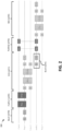
- Figure 6 is a schematic block diagram 600 of a circuit that propagates the Pauli operator X C through the circuit.
- One can check that the circuit maps X C onto X C ⁇ i 1 m X T i as expected
- This multi-target CNOT gate can be implemented in a grid of Majorana qubits where all single-qubit measurement M X , M Z are available, as well as two-qubit measurement M P 1 P 2 of Pauli operators P 1 P 2 between neighbors qubits.
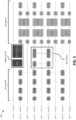
- FIG. 7 is a block diagram 700 representing the planar layout for the multi-target CNOT gate of Figure 6 .
- example methods for performing aspects of the disclosed embodiments are disclosed.
- the particular embodiments described should not be construed as limiting, as the disclosed method acts can be performed alone, in different orders, or at least partially simultaneously with one another. Further, any of the disclosed methods or method acts can be performed with any other methods or method acts disclosed herein.
- Figure 8 is an example method for performing a layout reduction technique for fault-tolerant quantum computing in accordance with an embodiment of the disclosed technology.
- the method is performed by one or more classical computing devices, at least some of which are in a configuration that can operate a quantum computer.
- a layout of an arbitrary quantum circuit is reduced to a layout of exponents of a multiple qubit Pauli matrix and measurements of a multiple qubit Pauli matrix.
- a quantum computer is configured to implement the reduced layout.
- qubits of the quantum computer comprise data qubits, interface qubits, and ancilla qubits.
- a graph of qubit connectivity satisfies a condition of providing an ancilla-path from one or more data qubits to the interface qubits.
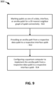
- Figure 9 is an example method for performing a layout technique for fault-tolerant quantum computing in accordance with an embodiment of the disclosed technology.
- the method is performed by one or more classical computing devices, at least some of which are in a configuration that can operate a quantum computer.
- qubits are marked as one of a data, interface, or ancilla qubit for a 2D nearest neighbor graph of qubit connectivity.
- an ancilla-path is provided from a respective data qubit to a respective interface qubit.
- a quantum computer is configured to implement the ancilla-path from a respective data qubit to a respective interface qubit.
- the method accounts for and avoids any broken qubits and satisfies a condition of providing an ancilla-path from a data qubit to the interface qubits.
- any of the methods described above can be performed in a system, comprising a quantum computing device; and one or more classical-computing devices, at least some of the one or more classical computing devices being programmed to perform any of the disclosed methods.
- any of the methods described above can be implemented as one or more classical-computer-readable-media storing classical-computer-executable instructions, which when executed by a classical computer cause the classical computer to perform any of the disclosed methods.
- a quantum circuit configured to apply an exponent of a multiple qubit Pauli matrix and measure a multiple qubit Pauli matrix.
- an ancilla-path is provided from data qubits to the interface qubits.
- the quantum circuit has a depth not depending on the number of vertexes.
- the quantum circuit uses single or low-depth multiple-target CNOT gates as a sub-circuits.
- Some embodiments comprise a quantum circuit configured to (a) provide a multi-target CNOT gate using a single-qubit and two-qubit Pauli measurements and single qubit Clifford gates; or (b) provide a multi-target CNOT gate using a single-qubit, Pauli measurements, single qubit Clifford gates and Controlled-Z gates.
- the quantum circuit provides a multi-target CNOT gate using a single-qubit and two-qubit Pauli measurements and single qubit Clifford gates, wherein the quantum circuit works with qubits for which a graph of qubit connectivity satisfies a condition of providing an ancilla-path from a target qubit to the control qubit.
- the quantum circuit provides a multi-target CNOT gate using a single-qubit and two-qubit Pauli measurements and single qubit Clifford gates, wherein the quantum circuit has a depth not depending on the number of vertexes.
- the quantum circuit is configured to provide a multi-target CNOT gate using a single-qubit, Pauli measurements, single qubit Clifford gates and Controlled-Z gates, and wherein the quantum circuit works with qubits for which graph of qubit connectivity satisfies a condition of providing an ancilla-path from a target qubit to the control qubit.
- the quantum circuit is configured to provide a multi-target CNOT gate using a single-qubit, Pauli measurements, single qubit Clifford gates and Controlled-Z gates, wherein the quantum circuit has a depth not depending on the number of vertexes.
- a further embodiment is a method that comprises implementing a product of exponents of commuting multiple-qubit Pauli matrices in low depth where non-clifford gates can be executed in parallel.
- An additional embodiment is a quantum circuit for providing a multi-target CNOT gate using a single-qubit and two-qubit Pauli measurements.
- the quantum circuit further comprises a 2-d nearest neighbor architecture.
- the quantum circuit comprises a 3-N grid of qubits with a center row or center column of data qubits, each respective data qubit further being directly connected to two ancilla qubits.
- the quantum circuit comprises a comb architecture with a center row or center column of data qubits, each respective data qubit further being directly connected to one ancilla qubits to thereby form the comb architecture.
- the quantum circuit is a low-constant-depth quantum circuit.
- the quantum circuit has a depth equal to a largest vertex degree of a tree describing the quantum circuit.
- a further embodiment comprises a quantum circuit for computing an exponent of a multiple qubit Pauli matrix.
- the multiple qubit Pauli matrix is a two-qubit Pauli matrix.
- the quantum circuit is a low-constant-depth quantum circuit.
- the quantum circuit has a depth equal to a largest vertex degree of a tree describing the quantum circuit.
- An additional embodiment is a method comprising: reducing a layout of an arbitrary quantum circuit to a layout of exponents of a multiple qubit Pauli matrix.
- a further embodiment is a method comprising implementing a product of exponents of commuting multiple-qubit Pauli matrices in low depth where non-clifford gates can be executed in parallel.
- An additional embodiment is a computer-implemented method that builds a data/ancilla qubit layout for a given graph of qubit connectivity and satisfies a condition of providing an ancilla-path from every data qubit to the interface qubits.
- the method accounts for and avoids any broken qubits.
- any of the methods described above can be implemented as one or more classical-computer-readable-media storing classical-computer-executable instructions, which when executed by a classical computer cause the classical computer to perform any of the disclosed methods.
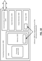
- FIG. 10 illustrates a generalized example of a suitable classical computing environment 1000 in which several of the described embodiments can be implemented.
- the computing environment 1000 is not intended to suggest any limitation as to the scope of use or functionality of the disclosed technology, as the techniques and tools described herein can be implemented in diverse general-purpose or special-purpose environments that have computing hardware.
- the computing environment 1000 includes at least one processing device 1010 and memory 1020.
- the processing device 1010 e.g., a CPU or microprocessor
- the memory 1020 may be volatile memory (e.g., registers, cache, RAM, DRAM, SRAM), non-volatile memory (e.g., ROM, EEPROM, flash memory), or some combination of the two.
- the memory 1020 stores software 1080 implementing tools for peforming any of the layout techniques for fault-tolerant quantum computers disclosed herein, using a classical computer and/or quantum computer.
- the memory 1020 can store software for controlling a quantum circuit to implement an embodiment of the disclosed approximation technique.
- the memory 1020 can also store software 1080 for synthesizing, generating (or compiling), and/or controlling quantum circuits as described herein.
- the computing environment 1000 includes storage 1040, one or more input devices 1050, one or more output devices 1060, and one or more communication connections 1070.
- An interconnection mechanism (not shown), such as a bus, controller, or network, interconnects the components of the computing environment 1000.
- operating system software provides an operating environment for other software executing in the computing environment 1000, and coordinates activities of the components of the computing environment 1000.
- the storage 1040 can be removable or non-removable, and includes one or more magnetic disks (e.g., hard drives), solid state drives (e.g., flash drives), magnetic tapes or cassettes, CD-ROMs, DVDs, or any other tangible non-volatile storage medium which can be used to store information and which can be accessed within the computing environment 1000.
- the storage 1040 can also store instructions for the software 1080 implementing tools for peforming any of the layout techniques for fault-tolerant quantum computers disclosed herein using a classical computer and/or quantum computer.
- the memory 1020 can store software for controlling a quantum circuit to implement an embodiment of the disclosed layout techniques.
- the storage 1040 can also store instructions for the software 1080 for synthesizing, generating (or compiling), and/or controlling quantum circuits as described herein.
- the input device(s) 1050 can be a touch input device such as a keyboard, touchscreen, mouse, pen, trackball, a voice input device, a scanning device, or another device that provides input to the computing environment 1000.
- the output device(s) 1060 can be a display device (e.g., a computer monitor, laptop display, smartphone display, tablet display, netbook display, or touchscreen), printer, speaker, or another device that provides output from the computing environment 1000.
- the communication connection(s) 1070 enable communication over a communication medium to another computing entity.
- the communication medium conveys information such as computer-executable instructions or other data in a modulated data signal.
- a modulated data signal is a signal that has one or more of its characteristics set or changed in such a manner as to encode information in the signal.
- communication media include wired or wireless techniques implemented with an electrical, optical, RF, infrared, acoustic, or other carrier.
- Computer-readable media are any available media (e.g., memory or storage device) that can be accessed within or by a computing environment.
- Computer-readable media include tangible computer-readable memory or storage devices, such as memory 1020 and/or storage 1040, and do not include propagating carrier waves or signals per se (tangible computer-readable memory or storage devices do not include propagating carrier waves or signals per se).
- program modules include routines, programs, libraries, objects, classes, components, data structures, and so on, that perform particular tasks or implement particular abstract data types.
- the functionality of the program modules may be combined or split between program modules as desired in various embodiments.
- Computer-executable instructions for program modules may be executed within a local or distributed computing environment.
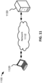
- Networked computing device 1120 can be, for example, a computer running a browser or other software connected to a network 1112.
- the computing device 1120 can have a computer architecture as shown in Figure 10 and discussed above.
- the computing device 1120 is not limited to a traditional personal computer but can comprise other computing hardware configured to connect to and communicate with a network 1112 (e.g., smart phones, laptop computers, tablet computers, or other mobile computing devices, servers, network devices, dedicated devices, and the like). Further, the computing device 1120 can comprise an FPGA or other programmable logic device.
- the computing device 1120 is configured to communicate with a computing device 1130 (e.g., a remote server, such as a server in a cloud computing environment) via a network 1112.
- a computing device 1130 e.g., a remote server, such as a server in a cloud computing environment
- the computing device 1120 is configured to transmit input data to the computing device 1130
- the computing device 1130 is configured to implement a quantum circuit control technique according to any of the disclosed embodiments and/or a circuit generation or compilation/synthesis methods for generating qunatum circuits for use with any of the techniques disclosed herein.
- the computing device 1130 can output results to the computing device 1120. Any of the data received from the computing device 1130 can be stored or displayed on the computing device 1120 (e.g., displayed as data on a graphical user interface or web page at the computing devices 1120).
- the illustrated network 1112 can be implemented as a Local Area Network (LAN) using wired networking (e.g., the Ethernet IEEE standard 802.3 or other appropriate standard) or wireless networking (e.g. one of the IEEE standards 802.11a, 802.11b, 802.11g, or 802.11n or other appropriate standard).
- wired networking e.g., the Ethernet IEEE standard 802.3 or other appropriate standard
- wireless networking e.g. one of the IEEE standards 802.11a, 802.11b, 802.11g, or 802.11n or other appropriate standard.
- at least part of the network 1112 can be the Internet or a similar public network and operate using an appropriate protocol (e.g., the HTTP protocol).
- Networked computing device 1220 can be, for example, a computer running a browser or other software connected to a network 1212.
- the computing device 1220 can have a computer architecture as shown in Figure 10 and discussed above.
- the computing device 1220 is configured to communicate with multiple computing devices 1230, 1231, 1232 (e.g., remote servers or other distributed computing devices, such as one or more servers in a cloud computing environment) via the network 1212.
- each of the computing devices 1230, 1231, 1232 in the computing environment 1200 is used to perform at least a portion of a quantum circuit control technique according to any of the disclosed embodiments and/or a circuit generation or compilation/synthesis methods for generating quantum circuits for use with any of the techniques disclosed herein.
- the computing devices 1230, 1231, 1232 form a distributed computing environment in which the quantum circuit control and/or generation/compilation/synthesis processes are shared across multiple computing devices.
- the computing device 1220 is configured to transmit input data to the computing devices 1230, 1231, 1232, which are configured to distributively implement such as process, including performance of any of the disclosed methods or creation of any of the disclosed circuits, and to provide results to the computing device 1220.
- Any of the data received from the computing devices 1230, 1231, 1232 can be stored or displayed on the computing device 1220 (e.g., displayed as data on a graphical user interface or web page at the computing devices 1220).
- the illustrated network 1212 can be any of the networks discussed above with respect to Figure 11 .
- an exemplary system for implementing the disclosed technology includes computing environment 1300.
- a compiled quantum computer circuit description (including quantum circuits generated by any of the disclosed layout techniques) can be used to program (or configure) one or more quantum processing units such that the quantum processing unit(s) implement the circuit described by the quantum computer circuit description.
- the environment 1300 includes one or more quantum processing units 1302 and one or more readout device(s) 1308.
- the quantum processing unit(s) execute quantum circuits that are precompiled and described by the quantum computer circuit description.
- the quantum processing unit(s) can be one or more of, but are not limited to: (a) a superconducting quantum computer; (b) an ion trap quantum computer; (c) a fault-tolerant architecture for quantum computing; and/or (d) a topological quantum architecture (e.g., a topological quantum computing device using Majorana zero modes).
- the precompiled quantum circuits, including any of the disclosed circuits can be sent into (or otherwise applied to) the quantum processing unit(s) via control lines 1306 at the control of quantum processor controller 1320.
- the quantum processor controller (CaP controller) 1320 can operate in conjunction with a classical processor 1310 (e.g., having an architecture as described above with respect to Figure 10 ) to implement the desired quantum computing process.
- the CaP controller 1320 further implements the desired quantum computing process via one or more CaP subcontrollers 1304 that are specially adapted to control a corresponding one of the quantum processor(s) 1302.
- the quantum controller 1320 facilitates implementation of the compiled quantum circuit by sending instructions to one or more memories (e.g., lower-temperature memories), which then pass the instructions to low-temperature control unit(s) (e.g., CaP subcontroller(s) 1304) that transmit, for instance, pulse sequences representing the gates to the quantum processing unit(s) 1302 for implementation.
- the CaP controller(s) 1320 and CaP subcontroller(s) 1304 operate to provide appropriate magnetic fields, encoded operations, or other such control signals to the quantum processor(s) to implement the operations of the compiled quantum computer circuit description.
- the quantum controller(s) can further interact with readout devices 1308 to help control and implement the desired quantum computing process (e.g., by reading or measuring out data results from the quantum processing units once available, etc.)
- compilation is the process of translating a high-level description of a quantum algorithm into a quantum computer circuit description comprising a sequence of quantum operations or gates, which can include the circuits as disclosed herein.
- the compilation can be performed by a compiler 1322 using a classical processor 1310 (e.g., as shown in Figure 10 ) of the environment 1300 which loads the high-level description from memory or storage devices 1312 and stores the resulting quantum computer circuit description in the memory or storage devices 1312.
- compilation and/or verification can be performed remotely by a remote computer 1360 (e.g., a computer having a computing environment as described above with respect to Figure 10 ) which stores the resulting quantum computer circuit description in one or more memory or storage devices 1362 and transmits the quantum computer circuit description to the computing environment 1300 for implementation in the quantum processing unit(s) 1302. Still further, the remote computer 1300 can store the high-level description in the memory or storage devices 1362 and transmit the high-level description to the computing environment 1300 for compilation and use with the quantum processor(s). In any of these scenarios, results from the computation performed by the quantum processor(s) can be communicated to the remote computer after and/or during the computation process.
- a remote computer 1360 e.g., a computer having a computing environment as described above with respect to Figure 10
- the remote computer 1300 can store the high-level description in the memory or storage devices 1362 and transmit the high-level description to the computing environment 1300 for compilation and use with the quantum processor(s).
- the remote computer can communicate with the CaP controller(s) 1320 such that the quantum computing process (including any compilation, verification, and CaP control procedures) can be remotely controlled by the remote computer 1360.
- the remote computer 1360 communicates with the CaP controller(s) 1320, compiler/synthesizer 1322, and/or verification tool 1323 via communication connections 1350.
- the environment 1300 can be a cloud computing environment, which provides the quantum processing resources of the environment 1300 to one or more remote computers (such as remote computer 1360) over a suitable network (which can include the internet).
- a cloud computing environment which provides the quantum processing resources of the environment 1300 to one or more remote computers (such as remote computer 1360) over a suitable network (which can include the internet).
Landscapes
- Engineering & Computer Science (AREA)
- Physics & Mathematics (AREA)
- Theoretical Computer Science (AREA)
- General Physics & Mathematics (AREA)
- General Engineering & Computer Science (AREA)
- Evolutionary Computation (AREA)
- Computing Systems (AREA)
- Mathematical Physics (AREA)
- Data Mining & Analysis (AREA)
- Software Systems (AREA)
- Artificial Intelligence (AREA)
- Condensed Matter Physics & Semiconductors (AREA)
- Mathematical Optimization (AREA)
- Computational Mathematics (AREA)
- Mathematical Analysis (AREA)
- Pure & Applied Mathematics (AREA)
- Computer Hardware Design (AREA)
- Architecture (AREA)
- Geometry (AREA)
- Computational Linguistics (AREA)
- Design And Manufacture Of Integrated Circuits (AREA)
- Management, Administration, Business Operations System, And Electronic Commerce (AREA)
- Semiconductor Integrated Circuits (AREA)
Abstract
Description
- This application claims the benefit of
U.S. Provisional Application No. 62/681,540, entitled "LAYOUTS FOR FAULT-TOLERANT QUANTUM COMPUTERS" and filed on June 6, 2018 - Disclosed herein are example layouts and layout generation techniques for fault-tolerant quantum computers. The particular embodiments described should not be construed as limiting, as the disclosed method acts can be performed alone, in different orders, or at least partially simultaneously with one another. Further, any of the disclosed methods or method acts can be performed with any other methods or method acts disclosed herein. Likewise, the disclosed combinations of features can include rearrangements of any novel or nonobvious combination or subcombination of features.
- One example embodiment comprises a method for performing a layout reduction technique for fault-tolerant quantum computing. In particular embodiments, the method is performed by one or more classical computing devices, at least some of which are in a configuration that can operate a quantum computer. In certain embodiments, a layout of an arbitrary quantum circuit is reduced to a layout of exponents of a multiple qubit Pauli matrix and measurements of a multiple qubit Pauli matrix; and a quantum computer is configured to implement the reduced layout. In particular implementations, qubits of the quantum computer comprise data qubits, interface qubits, and ancilla qubits. In further implementations, a graph of qubit connectivity satisfies a condition of providing an ancilla-path from one or more data qubits to the interface qubits.
- Another example embodiment comprises another method for performing a layout technique for fault-tolerant quantum computing. In particular embodiments, the method is performed by one or more classical computing devices, at least some of which are in a configuration that can operate a quantum computer. In certain embodiments, qubits are marked as one of a data, interface, or ancilla qubit for a 2D nearest neighbor graph of qubit connectivity; an ancilla-path is provided from a respective data qubit to a respective interface qubit; and a quantum computer is configured to implement the ancilla-path from a respective data qubit to a respective interface qubit. In certain implementations, the method accounts for and avoids any broken qubits and satisfies a condition of providing an ancilla-path from a data qubit to the interface qubits.
- Any of the methods described above can be performed in a system, comprising a quantum computing device; and one or more classical-computing devices, at least some of the one or more classical computing devices being programmed to perform any of the disclosed methods.
- Additionally, any of the methods described above can be implemented as one or more classical-computer-readable-media storing classical-computer-executable instructions, which when executed by a classical computer cause the classical computer to perform any of the disclosed methods.
- Further embodiments comprise, a quantum circuit configured to apply an exponent of a multiple qubit Pauli matrix and measure a multiple qubit Pauli matrix. In some implementations, an ancilla-path is provided from data qubits to the interface qubits. In further implementations, the quantum circuit has a depth not depending on the number of vertexes. In some implementations, the quantum circuit uses single or low-depth multiple-target CNOT gates as a sub-circuits.
- Some embodiments, comprise a quantum circuit configured to (a) provide a multi-target CNOT gate using a single-qubit and two-qubit Pauli measurements and single qubit Clifford gates; or (b) provide a multi-target CNOT gate using a single-qubit, Pauli measurements, single qubit Clifford gates and Controlled-Z gates. In some implementations, the quantum circuit provides a multi-target CNOT gate using a single-qubit and two-qubit Pauli measurements and single qubit Clifford gates, wherein the quantum circuit works with qubits for which a graph of qubit connectivity satisfies a condition of providing an ancilla-path from a target qubit to the control qubit. In further implementations, the quantum circuit provides a multi-target CNOT gate using a single-qubit and two-qubit Pauli measurements and single qubit Clifford gates, wherein the quantum circuit has a depth not depending on the number of vertexes. In some implementations, the quantum circuit is configured to provide a multi-target CNOT gate using a single-qubit, Pauli measurements, single qubit Clifford gates and Controlled-Z gates, and wherein the quantum circuit works with qubits for which graph of qubit connectivity satisfies a condition of providing an ancilla-path from a target qubit to the control qubit. In further implementations, the quantum circuit is configured to provide a multi-target CNOT gate using a single-qubit, Pauli measurements, single qubit Clifford gates and Controlled-Z gates, wherein the quantum circuit has a depth not depending on the number of vertexes.
- The foregoing and other objects, features, and advantages of the disclosed technology will become more apparent from the following detailed description, which proceeds with reference to the accompanying figures.
-
-
Figure 1 is a schematic block diagram that represents the circuit realizing a CNOT gate between the top qubit and the bottom qubit. -
Figure 2 is a schematic block diagram showing an example of providing a multi-target CNOT gate by measurement. -
Figure 3 is a schematic block diagram illustrating a modified version ofFigure 2 after moving the purple measurement M Z1 Z4 to the left to parallelize the final red block between the ancillas and the targets. -
Figure 4 is a schematic block diagram illustrating further modifying the initial measurements to parallelize the purple block between the control qubit and the ancillas (The effect of this parallelization appears only when more than two targets are present). -
Figure 5 is a schematic block diagram of a further general circuit in accordance with an embodiment of the disclosed technology. -
Figure 6 is a schematic block diagram of an example circuit that propagates a Pauli operator XC . -
Figure 7 is a block diagram representing the planar layout for the multi-target CNOT gate ofFigure 6 . -
Figure 8 is a flow chart showing a general method for performing embodiments of the disclosed technology. -
Figure 9 is a flow chart showing a further general method for performing embodiments of the disclosed technology. -
Figure 10 illustrates a generalized example of a suitable classical computing environment in which aspects of the described embodiments can be implemented. -
Figure 11 shows an example of a possible network topology (e.g., a client-server network) for implementing a system according to the disclosed technology. -
Figure 12 shows another example of a possible network topology (e.g., a distributed computing environment) for implementing a system according to the disclosed technology. -
Figure 13 shows an exemplary system for implementing the disclosed quantum-computing technology. - As used in this application, the singular forms "a," "an," and "the" include the plural forms unless the context clearly dictates otherwise. Additionally, the term "includes" means "comprises." Further, the term "coupled" does not exclude the presence of intermediate elements between the coupled items. Further, as used herein, the term "and/or" means any one item or combination of any items in the phrase.
- Although the operations of some of the disclosed methods are described in a particular, sequential order for convenient presentation, it should be understood that this manner of description encompasses rearrangement, unless a particular ordering is required by specific language set forth below. For example, operations described sequentially may in some cases be rearranged or performed concurrently. Moreover, for the sake of simplicity, the attached figures may not show the various ways in which the disclosed systems, methods, and apparatus can be used in conjunction with other systems, methods, and apparatus. Additionally, the description sometimes uses terms like "produce" and "provide" to describe the disclosed methods. These terms are high-level abstractions of the actual operations that are performed. The actual operations that correspond to these terms will vary depending on the particular implementation and are readily discernible by one of ordinary skill in the art.
- Let I, X, Y and Z denote single qubit Pauli matrices. All single qubit Pauli matrices are Hermitian matrices. Square of every Pauli matrix is equal to I. A multiple qubit Pauli matrix is a tensor product (denoted as ⊗) of single qubit Pauli matrices. Notation Xk, Yk, Zk refers to a multiple qubit Pauli matrix with X, Y and Z on qubit k and I on all other qubits. For example X 2 as 3 qubit Pauli matrix refers to the matrix:

- Multiple qubit Pauli matrices are also Hermitian and their square is the identity matrix. Below, the multiple qubit Pauli matrix will simply be called a Pauli matrix. I is used for the identity matrix on any number of qubits. The dimension of I will be clear from the context.
- The notation P| k is used for the k-th component of the multi-qubit Pauli matrix. For example, for P = XaYbZc, P| a = X, P| b = Y and P| c = Z.
- For any square matrix A, Tr(A) is the sum of the diagonal elements of A. For arbitrary square matrices A, B it is the case that Tr(AB) = Tr(BA). In addition, Tr(A ⊗ B) = Tr(A) · Tr(B).
- Orthogonal projector is a Hermitian matrix C with property C 2 = C. Tr(C) is equal to the dimension of the subspace that C projects onto.
- Matrices A and B commute if AB = BA. Matrices A and B anti-commute if AB = -BA. Any two Pauli matrices either commute or anti-commute.
- Plus state |+〉 is

- Hk is the Hadamard gate on qubit k. It is equal to

- One-qubit Clifford gates are

- CZij is Controlled-Z gate on qubits i and j. It is equal to (I + Zi + Zj - ZiZj ).
- Hermitian matrix M stabilizes state |ψ〉 if the state |ψ〉 is +1 eigenvector of M. In other words, M|ψ〉 = |ψ〉.
- n-qubit cat state is the state

- Let U be some unitary and let Q = UPU † , it will be said that U maps P to Q.
- In this section, example embodiments of algorithms that solve special cases of the following problem are disclosed:
Problem 3.1 (Layout problem for a graph). Let (V, E) be a graph and V rot be a subset of V. Vertexes are qubits. Consider quantum computation that uses one and two qubits Clifford operations, single qubit rotations exp(iφZ) and single qubit measurements. Perform a quantum computation that produces the same measurement outcomes using: - one qubits measurements and one qubit Clifford unitaries,
- either (A) controlled-Z gates or (B) two qubit measurements on qubits connected by an edge
- single qubit rotations exp(iφZ) can only be performed on subset V rot
- Using two (e.g., only two) qubit measurements on every edge is more restrictive. Any two qubit measurement can always be performed using two Controlled-Z gates, one measurement, and a single qubit Clifford gate. However, it is not possible to perform a Controlled-Z gate on two qubits by only measuring these two qubits. Restricting the qubits on which single qubit rotations can be performed reflects the fact that performing these rotations on a fault-tolerant quantum computer typically uses resource states that are usually produced in a dedicated part of the computer. Subset V rot represents qubits to which it is easy to deliver resource states needed to implement the rotations.
- The above problem can also be reduced to the case where V rot comprises one element r and (V, E) is a tree with the root r. Indeed, for any graph (V, E) one can compute a spanning tree with root r. First, the solution for this case is described.
- The first part of an example solution is to transform quantum computation to a canonical from. Here, the notation M (a, P) = (I + aP)/2 is used for the measurement of any multiple qubit Pauli operator P with outcome a = ±1. Suppose one has n qubit quantum computation described as:


- One can rewrite quantum computation (1) as:

- Using properties of measurement and exponential (2) one can further rewrite computation as:

- One can transform any quantum computation to a sequence of exponentials and measurements of multiple-qubit Clifford operation and the Clifford gate in the end. The Clifford gate in the end does not need to be executed because information is not extracted from the quantum computer after executing it.
- To perform an arbitrary computation under constraints described in Problem 3.1, it is sufficient to be able to perform measurements M(a, P) and exp(iφP) for arbitrary Pauli matrices supported on certain qubits V data ⊂ V. The size of subset V data determines a maximal number of qubits one can use for computation. It is sufficient to be able to perform a Clifford C and C † such that CZrC † = P under constraints on two qubit operations described in Problem 3.1. Such Clifford operations can be constructed using multi-target Controlled-Z gates as described in
Section 4. Table 1 and Table 2 show the programs for such a Clifford C operation that uses multiple-target Controlled-Z gates. The program of Table 1 applies Controlled-Z gates on edges of the tree, and the program of Table 2 applies two qubit measurements. When using this construction for Clifford C, set V data corresponds to all leaves of the tree except the root. - In
Section 5, a description is provided as to how to construct a tree with a high ratio of the number of leaves to the number of vertexes in 2D nearest neighbor architecture. Also considered is the case when fraction of the qubits in 2D nearest neighbor architecture is broken. It was found that when the fraction of broken is above 90%, one can still utilize good amount of qubits for computation.
- This section describes two ways of performing low-depth multi-target Controlled-Z gates. One is suitable for an architecture that has native Controlled-Z gates. Another one is for the architecture with two qubit operations restricted to only measurements of two qubit Pauli matrices. Notable for both is low depth circuit for cat state preparation and low depth circuit for fanout gate. In the following, qubits are considered to be vertexes of a tree and two qubit operations are allowed only


- The next proposition shows that the circuit depth required to prepare cat state on a tree does not depend on the number of tree vertexes.
- Proposition 4.1 (Low depth cat state preparation). Let (V, E) be a tree. Vertexes of the tree correspond to qubits. All the qubits are in plus state. One can only apply the following operations:
- measure observable Z ⊗ Z on qubits connected by an edge,
- apply Pauli X to any of the qubits except chosen in advance qubit w
- Then the cat state on qubits corresponding to vertexes can be prepared using |E| = |V| - 1 of Z ⊗ Z measurements, in depth equal to the largest vertex degree. In addition, one requires at most |V| - 1 Pauli X operations performed all in parallel. The pseudo-code for cat state preparation is given in Table 3.
- Proof. First, it will be shown that the procedure on Table 3 indeed prepares the cat state. Recall that cat state


- Indeed, the above implies that |ψ〉 is stabilized by the following projector:

- Next, expand the above product into sum of Pauli matrices. Use |E| = |V| - 1 and that all non-identity Pauli matrices have trace zero to check that Tr(P) = 1. Conclude that P fixes one dimensional sub-space.
- Initializing all qubits to |+〉 state ensures that their joint state is stabilized by Π v∈ V Xv. Measuring ZuZv for (u, v) ∈ E ensures that the state is +1 or -1 eigenstate of ZuZv . Note that because all constraints commute, adding a new one via measurement preserves all previous constraints. By the time all measurements were performed and the edges labeled, the state of the qubits |φ〉 satisfies the following constraints:

- It remains to fix the -1 signs. This can be done by applying single qubit Pauli X operators to vertexes. One can label vertex with 0 if one does not apply X to it, and with 1 if one does. This changes the signs in the following way:

- The label assignment can be found by one tree traversal, for example, using a depth first search. The label of the tree root can be chosen to be zero. The label of each vertex is computed based on the label of the parent and the label of the edge connecting the vertex and its parent.
- Finally note that edges of each color do not share vertexes. For this reason, measurements on corresponding qubits can all be performed in parallel. This implies that the depth of the measurement part of the cat state preparation is equal to the chromatic number of the tree which is the largest vertex degree plus one. □
- Given an n-qubit cat state it is sufficient to perform one two-qubit measurement to get a fanout gate

- Proposition 4.2 (Unitary operations via measurement). Let |ψ〉 be a multiple qubit state and P be a multiple qubit Pauli matrix that stabilizes |ψ〉 (e.g., P|ψ〉 = |ψ〉). Let Q be another multiple qubit Pauli matrix that anti-commutes with P. Then the probability of measuring +1 for observable Q of |ψ〉 is 1/2. Moreover, if the measurement outcome is -1, then applying P conditioned on the outcome -1 is equivalent to measuring +1. Under above conditions, one can always deterministically apply the following transformations to |ψ〉 via measurement:

- Proof. First, the probability of measuring +1 is 1/2 is shown. One can show this by showing the probabilities of measuring +1 and -1 are equal. Recall that the probability of measuring ±1 is


- One can see that when the measurement outcome is +1, the state is transformed according to (3). Next check that this is again the case when the measurement outcome is -1 and apply correction P.

- If the measurement outcome was -1, one can apply correction P and the state becomes:

- In the above, the anti-commutativity of P, Q was used and the fact that P stabilizes |ψ〉. Finally, one can note that (I + Q)|ψ〉 = (I + QP)|ψ〉 and use the fact that for any matrix A that squares to minus identity exp(φA) = I cos(φ) + A sin(φ). □
- It has been shown that under the conditions of Proposition 4.2 a measurement with classical feedback is equivalent to a unitary transformation. This is because QP is anti-hermitian matrix and
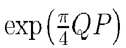
- The above discussion motivates the introduction of operation MeasurePlusOne(Q/P) (see Table 4). It performs operation given by Equation (3), given the state to which it is applied stabilized by P. In other words, operation MeasurePlusOne always projects the state onto +1 eigensubspace of Q. One can call P a constraint on the state.
- Now it is shown how MeasurePlusOne can be used to perform fanout gate.
- Proposition 4.3 (Low depth fanout). Let (V, E) be a tree. Vertexes of the tree correspond to qubits. All qubits except the root of the tree are in |+〉 state. One can only apply the following operations:
- measure observable Z ⊗ Z on qubits connected by an edge,
- apply Pauli X to any of the qubits.
- Proof. The correctness of operation Fanout1 in Table 5 is first shown. Next, it is shown that it is equivalent to operation Fanout described on the same table. The claim of the proposition regarding depth of Z ⊗ Z measurements follows from the fact that the number of colors in the edge coloring of the tree is equal to the maximal vertex degree plus one.
- Let state of the root vertex be α|0〉 + β|1〉. According to Proposition 4.2, the last three lines of operation Fanout1 on Table 4 deterministically project on +1 eigenspace of ZrZr'. This is because cat state is stabilized by the product of X over all non-root vertexes of the tree and this product anti-commutes with ZrZr' . Therefore after last three lines of Fanout1 the state of all qubits becomes:

- This is because projector (I + Z 1 Z 2)/2 selects computational basis states with first two bits equal:

- Next, a check is made that the operations Fanout and Fanout1 on Table 5 are equivalent. First, one can inline CatStatePrep. Next, one can observe that there is no X correction performed on vertex r' before measuring ZrZ r'. Therefore measurement ZrZr' can be performed together with all other measurements. Finally, X corrections applied in the end of CatStatePrep are combined with application of the X corrections in the end of Fanout1 operation. □
- Next, a description is provided as to how to use the fanout gate to perform multiple target Controlled-Z. One can start with the case that is more suitable for the architecture with native Controlled-Z gates.
- Proposition 4.4 (Low depth multiple target Controlled-Z). Let (V, E) be a tree. Vertexes of the tree correspond to qubits. Qubits that are not tree leaves are in a plus state. Measurements of observable Z ⊗ Z and Controlled-Z gates can only be applied to qubits connected by an edge. Programs given on Table 6 perform multiple target Controlled-Z gate with tree root being control and the rest of the leaves being targets. The rest of the tree vertices are returned back to plus state.
- The depth of joint measurements is at most the largest vertex degree. The depth of Controlled-Z gates is at most the largest vertex degree. The total number of joint measurements and Controlled-Z operations applied equals to the total number of edges. The depth of X measurements is one.

- Proof. It is first shown that program MultipleTargetControlledZ1 on Table 6 performs multiple target Controlled-Z gate and satisfies required postcondition. Next, it is shown that the program is equivalent to MultipleTargetControlledZ. Finally, the depth of the operations performed in MultipleTargetControlledZ are counted.
- Recall that on computational basis states multiple-target Controlled-Z gate acts as following:

- Above the first qubit is control and the rest are targets. In this case, control and targets are leaves of the tree. One also has, say m, other qubits that are not leaves of the tree. Using fanout operation, the state transforms as:

- After the first foreach loop the state becomes:

- This is because Controlled-Z gates are performed between each of the target qubits and some qubit that is not a leaf of the tree and is in state |c〉. Note that the above state (4) is +1 eigenstate of all ZrZv operators, where r is a tree root and control qubit and v are non-leaf qubits. For this reason, one can use MeasurePlusOne operations to set all non-leaf qubits back to plus state. It is important to note that setting one of the non-leaf qubits to plus state does not violate ZrZv constraints on other qubits and therefore this can be done in parallel.
- To obtain MultipleTargetControlledZ program, one can inline all calls to MeasurePlusOne. Next one can observe that all measurements can be performed first and the correction can be performed afterwards. As shown below, one can also collect together all the corrections applied to the root vertex so the correction can be applied once.
- To count the depth of Z ⊗ Z measurements, one can observe that they are all performed within Fanout operation and the larges vertex degree of (V', E') is at most largest vertex degree of (V, E). The depth of Controlled-Z operations performed is at most number of edges that share a vertex that is the largest degree of a vertex. □
- The rest of this section is devoted to the architectures with two qubit measurements only. First recall how to perform Controlled-Z gate in this architectures using one extra qubit. It is convenient to use MeasurePlusOne(Q/P) to concisely express this result. This result will also help one to get the insight needed for multiple target Controlled-Z.
- Proposition 4.5. Consider three qubits a, b, c, with qubit a in |+〉 state, then the operation:
1 operation ControlledZbyMeasurement (c, t, a) 2 MeasurePlusOne (ZaZt /Xa ) 3 H a4 MeasurePlusOne(ZaZc / ZtXa ) 5 MeasurePlusOne(Xa /ZaZc ) - Proof. Let one first check that all the MeasurePlusOne can be applied. The qubit a is in |+〉, therefore the input state is stabilized by Xa. After the first step, as the result of the measurement, the overall state commutes with ZbZa. After applying the Hadamard to the second qubit, the state commutes with

step 4. - Now it will be shown that the Controlled-Z gate was indeed performed. It is sufficient to consider the case when all three qubits are in a tensor product state. Suppose the qubit t is in state αt |0〉 + βt |1〉. After
Step 1, the state of the qubits t, a becomes:
- After
Step 2 it is (up to normalization by

- Suppose qubit c is in state αc |0〉 + βc |1〉, then after
Step 3, the state of all three qubits becomes:
- Finally, measuring Xa transform the state into

- One can see that the state of the second qubit is |+〉 and the joint state of the first and the third qubits is

- Let one compare above program for Controlled-Z via measurement to version of MultipleTargetControlledZ operation applied to a tree with three vertexes c, t, a and edges (c, a)and (a, t):
1 MeasurePlusOne (ZaZt /Xa ) # Fanout call corresponds to one operation 2 Controlled- Z a,c3 MeasurePlusOne(Xa /ZaZt ) - The difference is that Hadamard followed by MeasurePlusOne(ZaZt /ZrXa ) are in place of the call to Controlled-Z. It turns out that they perform a unitary similar to Controlled-Z.
- Proposition 4.6. The following two operations H 2 ; MeasurePlusOne(Z 2 Z 3/Z 1 X 2) map computational basis states |aab〉 to (-1) ab |abb〉 for a, b zero or one.
- Proof. Applying Hadamard gate transforms input state into:

- The result of MeasurePlusOne(Z 3 Z 2/Z 1 X 2) is:

- This is because (I + Z 2 Z 3)/2 projects on the span of |00〉, |11〉. □
- Using this operation, one can construct multi-target Controlled-Z gate that uses only joint measurements and single qubit operations.

- Proposition 4.7 (Low depth multiple target Controlled-Z by measurement). Let (V, E) be a tree such that all it leaves except the root are connected to a vertex of degree two. In other words, non of these leaves connected to the same vertex. Vertexes correspond to qubits. All non-leaf qubits are in a plus state. The program MultipleTargetControlledZMeasure in Table 7 performs multiple target controlled Z gate with root being control and the rest of the leaves being targets. The measurement depth is at most the largest vertex degree plus two.
- Proof. Consider how MultipleTargetControlledZMeasure operation acts on inputs from computational basis. For each non-root leaf, in other words a target of control operations there is a unique vertex connected to it in a plus state. The state of such a pair in the beginning of the computation is |t 1〉|+〉. One can order qubits in the following way. First goes the control qubit, next pairs corresponding to each target qubit and the qubit connected to it, next the rest of the qubits. The state of all the qubits in the beginning of the computation is:

- After applying the fanout operation, the state becomes:

- After the first foreach loop, according to Proposition 4.6, the state of the qubits becomes:

- Now one can see that all the constraints in MeasurePlusOne operations in the last two foreach loops are satisfied by the state above. States |tk 〉|tk 〉 satisfy ZvZv' constraint appearing in the second foreach loop and state |c〉|c〉 satisfy constraints ZvZr appearing in the third foreach loop. After applying last two foreach loops the state of the qubits becomes

- The last two foreach loops can be performed in parallel because they involve different qubits. Each of foreach loops has measurement depth one. Therefore the overall measurement depth is the measurement depth of fanout operation plus two. □
- All data qubits should be connected to an interface qubit with a path of ancillas. Thus, only a fraction of all qubits can be data qubits, with the rest being used as ancillas for connectivity. Given a rectangular field of qubits with a nearest neighbor (each internal qubit has 4 neighbors) architecture, the most data qubits one can get is 2/3 of the total number of qubits. This is because an ancilla (barring the edges) can have at most 2 data qubits attached to it with the other two connections being used up to attach to two other ancillas.
- An ideal field configuration would be a 3×N grid of qubits where the center row consists of ancillas and top and bottom rows are data qubits. This would achieve a perfect 2/3 ratio of data qubits to total qubits.
- Assuming N×N grid of qubits, the best configuration to achieve the highest data qubits ratio is a comb, where the second column and
qubits 2 to N in every third row of qubits, starting fromrow # 2, are ancillas. The first row is reserved for interface qubits, and the rest are data qubits. For the calculations here, interface qubits to be data qubits are counted. In this configuration the ratio of data qubits to total qubits is (2N - 1)/3N, or 2/3 - 1/3N which is very close to 2/3. - The physical qubits have some probability of failure. Some of the qubits in a perfect rectangular grid may be dead (unsuitable for use). This not only decreases the number of available qubits, but also breaks connectivity between the remaining ones. For example, a path of ancillas may have a dead qubit in it, severing part of the line and breaking connectivity of the corresponding data qubits to the interface qubit.
- An algorithm to create an optimal layout of qubits given an irregular qubit graph is desirable. However, such an algorithm will require non-polynomial execution time, making it impractical. In accordance with the disclosed technology, a heuristic-based algorithm is provided that is close to optimal.
- Given a starting layout of a comb described above, the algorithm determines pieces of the graph disconnected from the interface qubits and tries to reconnect them enabling as many data qubits as possible. Starting from the interface qubit, one can mark continuous horizontal ancilla line segments as powered if they are connected to the interface. For each powered segment, one can queue all possible vertical routes that can extend from it. The routes that start at the ends of the segments go into the high-priority queue, and the rest into normal priority queue.
- Then, for each queued route (starting with high priority ones), one can determine if this route connects a previously unpowered ancilla segment, and if yes, accept the route, mark ancilla segment as powered, and add more potential routes starting from the newly powered segment to the queues. Each route that was accepted, converts two data qubits into ancillas. This continues until the queues are empty. Routes at the ends of segments are preferable, because they provide power to one or two additional data qubits (next to the dead ancilla), while routes spawning from mid-segments do not.
- Each dead data qubit causes a loss of one data qubit in our ratio. Each dead ancilla causes two data qubits to be unpowered, and an ancilla segment to be detached. Reattaching the ancilla segment requires use of two data qubits and is likely to power back one of the disconnected qubits. Thus, each dead ancilla is likely to result in a loss of 3 data qubits.
- This section discloses further details for implementing multi-target CNOT gates in Majorana architectures as can be used in embodiments of the disclosed technology.
- 6.1. Introduction. In a measurement based architecture such as a lattice of Majorana qubits, a CNOT gate can implemented by a sequence of four measurements using an ancilla qubit. Applying this circuit sequentially, one can implement a mutli-target CNOT gate with m targets in time linear in m, in depth 4m. In this section, a constant depth implementation for a multi-target CNOT gate based on single-qubit and two-qubit measurements is disclosed. The circuit has depth five in term of the number of levels of measurements (three two-qubit measurements and two single-qubit measurement). It requires one ancilla per target. This implementation is well suited for a grid of Majorana qubits.
- The following circuits are made with single-qubit Pauli measurements and two-qubit Pauli measurements. Each measurement M is a followed by a Clifford update U(P) which means that the Clifford operation P is a classically controlled gate that is applied only if the outcome of the measurement M is 1. The update U(P) is represented in the circuit as a box identical to the preceding measurement box for M but it does not necessarily acts only on the support of M. We are particularly interested in the context of Majorana qubits. Then, single-qubit Clifford operations can be realized without any physical action on the qubits by a change of frame. In particular all Clifford updates are free. This is why the depth is considered as the number of levels of measurement.
- 6.2. CNOT gate by measurement. In this subsection, recall the implementation of a CNOT gate using single-qubit and two-qubit measurements and an ancilla qubit.
Figure 1 is a schematic block diagram 100 that represents the circuit realizing a CNOT gate between the top qubit and the bottom qubit. The middle qubit is an ancilla require for the CNOT gate. More specifically, the blue gates prepare the ancilla qubit, and the purple gates entangle it with the control qubit and the red gates act on the ancilla and the target qubits. - Denote by |ψ〉 = α|0〉 + β|1〉 the contol qubit (qubit 1) and let |ϕ〉 = α'|0〉 + β'|1〉 be the target qubit (qubit 3). One can check that the circuit of
Figure 1 realizes a CNOT gate. In order to simplify the calculation, one can show that without the H-conjugation on the last qubit, the circuit realizes the CZ-gate. Adding the two H gate provides the CNOT gate. - The first measurement MX, followed by the update U(Z 2) in case of
outcome 1, prepares the ancilla qubit in the state |+〉. The combined state ofqubits 
- Measuring Z 1 Z 2 with outcome 0, projects the state of
qubit state 
outcome 1 is obtained, one gets the state α|01〉 + β|10〉 that is mapped onto |ψ 1〉 by the update U(X2 ). - The gate H 2 leads to |ψ 2〉 = α|00〉 + α|01〉 + β|10〉 + (-1)/β|11〉 on the first two qubits, and (without considering H 3) the three-qubits state is then

- If the outcome of M Z
2 Z3 is 0, then the post-measurement state is
outcome 1 is measured, the state after measurement is then
- Finally, get rid of the ancilla by measuring X. Assuming that the outcome is 0, one obtains the following state on
qubit 

- This proves that the circuit of
Figure 1 realizes the CNOT gate. - 6.3. Multi-target CNOT gate. A mutli-target CNOT gate applies a X gate to a set of m qubits q 1 , ... , qm, controlled on the state of a unique control qubit q 0. Naively, it can be realized by a sequence of m CNOT gates, CNOT(q 0, qi ) for i = 1, . . . , m. The depth of the multi-target CNOT gate is therefore at most linear in the number of targets. In this section, it is shown how to realize a multi-target gate in constant depth using one ancilla qubit for each target. While the same ancilla qubit can be reused for the sequential implementation of m CNOT gates, m ancillas are consumed for a constant depth implementation.
- The transformation of the sequential implementation used to reduce the depth of the circuit to a constant is shown in
Figures 2-4 in the case of a two-targets CNOT gate. -
Figure 2 is a schematic block diagram 200 showing an example of providing a multi-target CNOT gate by measurement. In particular, block diagram 200 illustrates an example sequential application of the CNOT circuit.Figure 3 is a schematic block diagram 300 illustrating a modified version of block diagram 200 after moving the purple measurement M Z1 Z4 to the left to parallelize the final red block between the ancillas and the targets.Figure 4 is a schematic block diagram 400 illustrating further modifying the initial measurements to parallelize the purple block between the control qubit and the ancillas (The effect of this parallelization appears only when more than two targets are present). - As illustrated, this transformation can be performed in two steps. First, one moves the join measurement MZZ between the control qubit and the ancillas to the past. This allows one to parallelize the final block of the circuit acting on the ancillas and the targets. In the second step, one can replace the m measurements

- The general circuit, represented in schematic block diagram 500 of
Figure 5 for four targets works as follows: - (i) [Ancilla preparation (blue)] Prepare a m-qubits cat state |0...0〉 + |1...1〉 over the m ancilla qubits a 1, ... , am , by measuring Z a
1 Z a2 , Z a2 Z a3 , ... , Z am-1 Zam . This can be done in two layers of measurements (followed by updates). - (ii) [Control block (purple)] Entangle the ancillas with the control qubit q 0 by measurement of Z g
0 Z a1 . The update U(X a1 X a2 ...Xam ) is applied in case of non-zero outcome. - (iii) [Target block (red)] Apply the target block of the standard CNOT by measurement in parallel to all the targets.
- In order to check that this circuit realizes the multi-target CNOT as claimed, it suffices to check that the circuit maps any Pauli operators onto the same Pauli operator as the multi-target CNOT gate. Given a Pauli matrix P, denote by PC the Pauli operator acting as P on the control qubit and acting trivially on all other qubits. Similarly Pa
i acts on the i-th ancilla and PTi on the i-th target. The multi-target CNOT gate is fully characterized by its action on Pauli operators as follows:


- One can easily check that the circuit satisfies these identities by propagating these Pauli operators through the circuit. For instance, one can propagate the operation XC through the circuit in
Figure 6 . In particular,Figure 6 is a schematic block diagram 600 of a circuit that propagates the Pauli operator XC through the circuit. One can check that the circuit maps XC onto
- This proves that it implements the desired multi-target CNOT operation.
- 6.4. Two-dimensional layout. This multi-target CNOT gate can be implemented in a grid of Majorana qubits where all single-qubit measurement MX, MZ are available, as well as two-qubit measurement M P
1 P2 of Pauli operators P 1 P 2 between neighbors qubits. - For instance, one can consider a line of m ancilla qubits where the cat state is prepared, connected to the control qubit through one of its endpoints. Each ancilla can reach a target qubit placed directly below it. This allows for a local implementation of the mutli-target CNOT gate described in this note.
Figure 7 is a block diagram 700 representing the planar layout for the multi-target CNOT gate ofFigure 6 . - In this section, example methods for performing aspects of the disclosed embodiments are disclosed. The particular embodiments described should not be construed as limiting, as the disclosed method acts can be performed alone, in different orders, or at least partially simultaneously with one another. Further, any of the disclosed methods or method acts can be performed with any other methods or method acts disclosed herein.
-
Figure 8 is an example method for performing a layout reduction technique for fault-tolerant quantum computing in accordance with an embodiment of the disclosed technology. In particular embodiments, the method is performed by one or more classical computing devices, at least some of which are in a configuration that can operate a quantum computer. - At 810, a layout of an arbitrary quantum circuit is reduced to a layout of exponents of a multiple qubit Pauli matrix and measurements of a multiple qubit Pauli matrix.
- At 812, a quantum computer is configured to implement the reduced layout.
- In particular implementations, qubits of the quantum computer comprise data qubits, interface qubits, and ancilla qubits. In further implementations, a graph of qubit connectivity satisfies a condition of providing an ancilla-path from one or more data qubits to the interface qubits.
-
Figure 9 is an example method for performing a layout technique for fault-tolerant quantum computing in accordance with an embodiment of the disclosed technology. In particular embodiments, the method is performed by one or more classical computing devices, at least some of which are in a configuration that can operate a quantum computer. - At 910, qubits are marked as one of a data, interface, or ancilla qubit for a 2D nearest neighbor graph of qubit connectivity.
- At 912, an ancilla-path is provided from a respective data qubit to a respective interface qubit. At 914, a quantum computer is configured to implement the ancilla-path from a respective data qubit to a respective interface qubit.
- In certain implementations, the method accounts for and avoids any broken qubits and satisfies a condition of providing an ancilla-path from a data qubit to the interface qubits.
- Any of the methods described above can be performed in a system, comprising a quantum computing device; and one or more classical-computing devices, at least some of the one or more classical computing devices being programmed to perform any of the disclosed methods.
- Additionally, any of the methods described above can be implemented as one or more classical-computer-readable-media storing classical-computer-executable instructions, which when executed by a classical computer cause the classical computer to perform any of the disclosed methods.
- Further embodiments comprise, a quantum circuit configured to apply an exponent of a multiple qubit Pauli matrix and measure a multiple qubit Pauli matrix. In some implementations, an ancilla-path is provided from data qubits to the interface qubits. In further implementations, the quantum circuit has a depth not depending on the number of vertexes. In some implementations, the quantum circuit uses single or low-depth multiple-target CNOT gates as a sub-circuits.
- Some embodiments, comprise a quantum circuit configured to (a) provide a multi-target CNOT gate using a single-qubit and two-qubit Pauli measurements and single qubit Clifford gates; or (b) provide a multi-target CNOT gate using a single-qubit, Pauli measurements, single qubit Clifford gates and Controlled-Z gates. In some implementations, the quantum circuit provides a multi-target CNOT gate using a single-qubit and two-qubit Pauli measurements and single qubit Clifford gates, wherein the quantum circuit works with qubits for which a graph of qubit connectivity satisfies a condition of providing an ancilla-path from a target qubit to the control qubit. In further implementations, the quantum circuit provides a multi-target CNOT gate using a single-qubit and two-qubit Pauli measurements and single qubit Clifford gates, wherein the quantum circuit has a depth not depending on the number of vertexes. In some implementations, the quantum circuit is configured to provide a multi-target CNOT gate using a single-qubit, Pauli measurements, single qubit Clifford gates and Controlled-Z gates, and wherein the quantum circuit works with qubits for which graph of qubit connectivity satisfies a condition of providing an ancilla-path from a target qubit to the control qubit. In further implementations, the quantum circuit is configured to provide a multi-target CNOT gate using a single-qubit, Pauli measurements, single qubit Clifford gates and Controlled-Z gates, wherein the quantum circuit has a depth not depending on the number of vertexes.
- A further embodiment is a method that comprises implementing a product of exponents of commuting multiple-qubit Pauli matrices in low depth where non-clifford gates can be executed in parallel.
- An additional embodiment is a quantum circuit for providing a multi-target CNOT gate using a single-qubit and two-qubit Pauli measurements. In some implementations, the quantum circuit further comprises a 2-d nearest neighbor architecture. In certain implementations, the quantum circuit comprises a 3-N grid of qubits with a center row or center column of data qubits, each respective data qubit further being directly connected to two ancilla qubits. In some implementations, the quantum circuit comprises a comb architecture with a center row or center column of data qubits, each respective data qubit further being directly connected to one ancilla qubits to thereby form the comb architecture. In certain implementations, the quantum circuit is a low-constant-depth quantum circuit. In some implementations, the quantum circuit has a depth equal to a largest vertex degree of a tree describing the quantum circuit.
- A further embodiment comprises a quantum circuit for computing an exponent of a multiple qubit Pauli matrix. In some implementations, the multiple qubit Pauli matrix is a two-qubit Pauli matrix. In certain implementations, the quantum circuit is a low-constant-depth quantum circuit. In further implementations, the quantum circuit has a depth equal to a largest vertex degree of a tree describing the quantum circuit.
- An additional embodiment is a method comprising: reducing a layout of an arbitrary quantum circuit to a layout of exponents of a multiple qubit Pauli matrix.
- A further embodiment is a method comprising implementing a product of exponents of commuting multiple-qubit Pauli matrices in low depth where non-clifford gates can be executed in parallel.
- An additional embodiment is a computer-implemented method that builds a data/ancilla qubit layout for a given graph of qubit connectivity and satisfies a condition of providing an ancilla-path from every data qubit to the interface qubits. In some implementations, the method accounts for and avoids any broken qubits.
- Again, any of the methods described above can be implemented as one or more classical-computer-readable-media storing classical-computer-executable instructions, which when executed by a classical computer cause the classical computer to perform any of the disclosed methods.
-
Figure 10 illustrates a generalized example of a suitableclassical computing environment 1000 in which several of the described embodiments can be implemented. Thecomputing environment 1000 is not intended to suggest any limitation as to the scope of use or functionality of the disclosed technology, as the techniques and tools described herein can be implemented in diverse general-purpose or special-purpose environments that have computing hardware. - With reference to
Figure 10 , thecomputing environment 1000 includes at least oneprocessing device 1010 andmemory 1020. InFigure 10 , this mostbasic configuration 1030 is included within a dashed line. The processing device 1010 (e.g., a CPU or microprocessor) executes computer-executable instructions. In a multi-processing system, multiple processing devices execute computer-executable instructions to increase processing power. Thememory 1020 may be volatile memory (e.g., registers, cache, RAM, DRAM, SRAM), non-volatile memory (e.g., ROM, EEPROM, flash memory), or some combination of the two. Thememory 1020stores software 1080 implementing tools for peforming any of the layout techniques for fault-tolerant quantum computers disclosed herein, using a classical computer and/or quantum computer. For example, thememory 1020 can store software for controlling a quantum circuit to implement an embodiment of the disclosed approximation technique. Thememory 1020 can also storesoftware 1080 for synthesizing, generating (or compiling), and/or controlling quantum circuits as described herein. - The computing environment can have additional features. For example, the
computing environment 1000 includesstorage 1040, one ormore input devices 1050, one ormore output devices 1060, and one ormore communication connections 1070. An interconnection mechanism (not shown), such as a bus, controller, or network, interconnects the components of thecomputing environment 1000. Typically, operating system software (not shown) provides an operating environment for other software executing in thecomputing environment 1000, and coordinates activities of the components of thecomputing environment 1000. - The
storage 1040 can be removable or non-removable, and includes one or more magnetic disks (e.g., hard drives), solid state drives (e.g., flash drives), magnetic tapes or cassettes, CD-ROMs, DVDs, or any other tangible non-volatile storage medium which can be used to store information and which can be accessed within thecomputing environment 1000. Thestorage 1040 can also store instructions for thesoftware 1080 implementing tools for peforming any of the layout techniques for fault-tolerant quantum computers disclosed herein using a classical computer and/or quantum computer. For example, thememory 1020 can store software for controlling a quantum circuit to implement an embodiment of the disclosed layout techniques. Thestorage 1040 can also store instructions for thesoftware 1080 for synthesizing, generating (or compiling), and/or controlling quantum circuits as described herein. - The input device(s) 1050 can be a touch input device such as a keyboard, touchscreen, mouse, pen, trackball, a voice input device, a scanning device, or another device that provides input to the
computing environment 1000. The output device(s) 1060 can be a display device (e.g., a computer monitor, laptop display, smartphone display, tablet display, netbook display, or touchscreen), printer, speaker, or another device that provides output from thecomputing environment 1000. - The communication connection(s) 1070 enable communication over a communication medium to another computing entity. The communication medium conveys information such as computer-executable instructions or other data in a modulated data signal. A modulated data signal is a signal that has one or more of its characteristics set or changed in such a manner as to encode information in the signal. By way of example, and not limitation, communication media include wired or wireless techniques implemented with an electrical, optical, RF, infrared, acoustic, or other carrier.
- As noted, the various methods, quantum circuit control techqniues, or compilation/synthesis techniques can be described in the general context of computer-readable instructions stored on one or more computer-readable media. Computer-readable media are any available media (e.g., memory or storage device) that can be accessed within or by a computing environment. Computer-readable media include tangible computer-readable memory or storage devices, such as
memory 1020 and/orstorage 1040, and do not include propagating carrier waves or signals per se (tangible computer-readable memory or storage devices do not include propagating carrier waves or signals per se). - Various embodiments of the methods disclosed herein can also be described in the general context of computer-executable instructions (such as those included in program modules) being executed in a computing environment by a processor. Generally, program modules include routines, programs, libraries, objects, classes, components, data structures, and so on, that perform particular tasks or implement particular abstract data types. The functionality of the program modules may be combined or split between program modules as desired in various embodiments. Computer-executable instructions for program modules may be executed within a local or distributed computing environment.
- An example of a possible network topology 1100 (e.g., a client-server network) for implementing a system according to the disclosed technology is depicted in
Figure 11 .Networked computing device 1120 can be, for example, a computer running a browser or other software connected to anetwork 1112. Thecomputing device 1120 can have a computer architecture as shown inFigure 10 and discussed above. Thecomputing device 1120 is not limited to a traditional personal computer but can comprise other computing hardware configured to connect to and communicate with a network 1112 (e.g., smart phones, laptop computers, tablet computers, or other mobile computing devices, servers, network devices, dedicated devices, and the like). Further, thecomputing device 1120 can comprise an FPGA or other programmable logic device. In the illustrated embodiment, thecomputing device 1120 is configured to communicate with a computing device 1130 (e.g., a remote server, such as a server in a cloud computing environment) via anetwork 1112. In the illustrated embodiment, thecomputing device 1120 is configured to transmit input data to thecomputing device 1130, and thecomputing device 1130 is configured to implement a quantum circuit control technique according to any of the disclosed embodiments and/or a circuit generation or compilation/synthesis methods for generating qunatum circuits for use with any of the techniques disclosed herein. Thecomputing device 1130 can output results to thecomputing device 1120. Any of the data received from thecomputing device 1130 can be stored or displayed on the computing device 1120 (e.g., displayed as data on a graphical user interface or web page at the computing devices 1120). In the illustrated embodiment, the illustratednetwork 1112 can be implemented as a Local Area Network (LAN) using wired networking (e.g., the Ethernet IEEE standard 802.3 or other appropriate standard) or wireless networking (e.g. one of the IEEE standards 802.11a, 802.11b, 802.11g, or 802.11n or other appropriate standard). Alternatively, at least part of thenetwork 1112 can be the Internet or a similar public network and operate using an appropriate protocol (e.g., the HTTP protocol). - Another example of a possible network topology 1200 (e.g., a distributed computing environment) for implementing a system according to the disclosed technology is depicted in
Figure 12 .Networked computing device 1220 can be, for example, a computer running a browser or other software connected to anetwork 1212. Thecomputing device 1220 can have a computer architecture as shown inFigure 10 and discussed above. In the illustrated embodiment, thecomputing device 1220 is configured to communicate withmultiple computing devices network 1212. In the illustrated embodiment, each of thecomputing devices computing environment 1200 is used to perform at least a portion of a quantum circuit control technique according to any of the disclosed embodiments and/or a circuit generation or compilation/synthesis methods for generating quantum circuits for use with any of the techniques disclosed herein. In other words, thecomputing devices computing device 1220 is configured to transmit input data to thecomputing devices computing device 1220. Any of the data received from thecomputing devices network 1212 can be any of the networks discussed above with respect toFigure 11 . - With reference to
Figure 13 , an exemplary system for implementing the disclosed technology includescomputing environment 1300. Incomputing environment 1300, a compiled quantum computer circuit description (including quantum circuits generated by any of the disclosed layout techniques) can be used to program (or configure) one or more quantum processing units such that the quantum processing unit(s) implement the circuit described by the quantum computer circuit description. - The
environment 1300 includes one or morequantum processing units 1302 and one or more readout device(s) 1308. The quantum processing unit(s) execute quantum circuits that are precompiled and described by the quantum computer circuit description. The quantum processing unit(s) can be one or more of, but are not limited to: (a) a superconducting quantum computer; (b) an ion trap quantum computer; (c) a fault-tolerant architecture for quantum computing; and/or (d) a topological quantum architecture (e.g., a topological quantum computing device using Majorana zero modes). The precompiled quantum circuits, including any of the disclosed circuits, can be sent into (or otherwise applied to) the quantum processing unit(s) viacontrol lines 1306 at the control ofquantum processor controller 1320. The quantum processor controller (CaP controller) 1320 can operate in conjunction with a classical processor 1310 (e.g., having an architecture as described above with respect toFigure 10 ) to implement the desired quantum computing process. In the illustrated example, theCaP controller 1320 further implements the desired quantum computing process via one or more CaP subcontrollers 1304 that are specially adapted to control a corresponding one of the quantum processor(s) 1302. For instance, in one example, thequantum controller 1320 facilitates implementation of the compiled quantum circuit by sending instructions to one or more memories (e.g., lower-temperature memories), which then pass the instructions to low-temperature control unit(s) (e.g., CaP subcontroller(s) 1304) that transmit, for instance, pulse sequences representing the gates to the quantum processing unit(s) 1302 for implementation. In other examples, the CaP controller(s) 1320 and CaP subcontroller(s) 1304 operate to provide appropriate magnetic fields, encoded operations, or other such control signals to the quantum processor(s) to implement the operations of the compiled quantum computer circuit description. The quantum controller(s) can further interact withreadout devices 1308 to help control and implement the desired quantum computing process (e.g., by reading or measuring out data results from the quantum processing units once available, etc.) - With reference to
Figure 13 , compilation is the process of translating a high-level description of a quantum algorithm into a quantum computer circuit description comprising a sequence of quantum operations or gates, which can include the circuits as disclosed herein. The compilation can be performed by acompiler 1322 using a classical processor 1310 (e.g., as shown inFigure 10 ) of theenvironment 1300 which loads the high-level description from memory orstorage devices 1312 and stores the resulting quantum computer circuit description in the memory orstorage devices 1312. - In other embodiments, compilation and/or verification can be performed remotely by a remote computer 1360 (e.g., a computer having a computing environment as described above with respect to
Figure 10 ) which stores the resulting quantum computer circuit description in one or more memory orstorage devices 1362 and transmits the quantum computer circuit description to thecomputing environment 1300 for implementation in the quantum processing unit(s) 1302. Still further, theremote computer 1300 can store the high-level description in the memory orstorage devices 1362 and transmit the high-level description to thecomputing environment 1300 for compilation and use with the quantum processor(s). In any of these scenarios, results from the computation performed by the quantum processor(s) can be communicated to the remote computer after and/or during the computation process. Still further, the remote computer can communicate with the CaP controller(s) 1320 such that the quantum computing process (including any compilation, verification, and CaP control procedures) can be remotely controlled by theremote computer 1360. In general, theremote computer 1360 communicates with the CaP controller(s) 1320, compiler/synthesizer 1322, and/orverification tool 1323 viacommunication connections 1350. - In particular embodiments, the
environment 1300 can be a cloud computing environment, which provides the quantum processing resources of theenvironment 1300 to one or more remote computers (such as remote computer 1360) over a suitable network (which can include the internet). - Having described and illustrated the principles of the disclosed technology with reference to the illustrated embodiments, it will be recognized that the illustrated embodiments can be modified in arrangement and detail without departing from such principles. For instance, elements of the illustrated embodiments shown in software may be implemented in hardware and vice-versa. Also, the technologies from any example can be combined with the technologies described in any one or more of the other examples. It will be appreciated that procedures and functions such as those described with reference to the illustrated examples can be implemented in a single hardware or software module, or separate modules can be provided. The particular arrangements above are provided for convenient illustration, and other arrangements can be used.

Claims (11)
- A method of implementing a multi-target CNOT gate in a quantum computer comprising m ancilla qubits a 1,...,am and m target qubits, the method comprising:preparing a cat state |0...0>+|1...1> over the m ancilla qubits a 1,...,am of the quantum computer by measuring Z a
1 Z a2 ,Z a2 Z a3 ,...,Z am-1 Zam ;entangling the m ancilla qubits with a control qubit q 0 of the quantum computer by measurement of Z q0 Z a1 ; andapplying, in parallel, m respective single-target CNOT gates to the m target qubits, each single-target CNOT gate i = 1, ..., m applied to the ith target qubit using ancilla qubit ai . - The method of claim 1, wherein each single-target CNOT gate is applied by measurement.
- The method of claim 1 or 2, wherein the m ancilla qubits and m target qubits are arranged in a grid, wherein the ith target qubit neighbours ancilla qubit ai in the grid, and control qubit q 0 neighbours ancilla qubit a 1 in the grid.
- The method of claim 3, wherein the grid is a 3xN grid of qubits where the centre row is ancilla qubits and top and bottom rows are data qubits, the data qubits comprising the target qubits.
- The method of claim 3, wherein the grid is an NxN grid of qubits, in which the second column and qubits 2 to N in every third row of qubits, starting from the second row, are ancilla qubits, wherein the first row is interface qubits, and the remaining qubits are data qubits, the data qubits comprising the target qubits.
- The method of any of claims 1 to 4, comprising applying an update U(X a
1 X a2 ...Xam ) in the case of a non-zero outcome of the measurement of Z q0 Z a1 . - A system comprising:a quantum computer comprising m ancilla qubits a 1,...,am and m target qubits; anda quantum processor controller configured to implement a multi-target CNOT gate in the quantum computer by:preparing a cat state |0...0>+|1...1> over the m ancilla qubits a 1,...,am of the quantum computer by measuring Z a
1 Z a2 ,Z a2 Z a3 ,...,Z am-1 Zam ;entangling the m ancilla qubits with a control qubit q 0 of the quantum computer by measurement of Z q0 Z a1 ; andapplying, in parallel, m respective single-target CNOT gates to the m target qubits, each single-target CNOT gate i = 1, ..., m applied to the ith target qubit using ancilla qubit ai. - The system of claim 7, wherein each single-target CNOT gate is applied by measurement.
- The system of claim 7 or 8, wherein the m ancilla qubits and m target qubits are arranged in a grid, wherein the ith target qubit neighbours ancilla qubit ai in the grid, and control qubit q 0 neighbours ancilla qubit a 1 in the grid.
- The system of claim 9, wherein the grid is a 3xN grid of qubits where the centre row is ancilla qubits and top and bottom rows are data qubits, the data qubits comprising the target qubits.
- The system of claim 9, wherein the grid is an NxN grid of qubits, in which the second column and qubits 2 to N in every third row of qubits, starting from the second row, are ancilla qubits, wherein the first row is interface qubits, and the remaining qubits are data qubits, the data qubits comprising the target qubits.
Applications Claiming Priority (3)
| Application Number | Priority Date | Filing Date | Title |
|---|---|---|---|
| US201862681540P | 2018-06-06 | 2018-06-06 | |
| PCT/US2019/035595 WO2019236712A2 (en) | 2018-06-06 | 2019-06-05 | Layouts for fault-tolerant quantum computers |
| EP19732200.1A EP3788564B1 (en) | 2018-06-06 | 2019-06-05 | Layouts for fault-tolerant quantum computers |
Related Parent Applications (2)
| Application Number | Title | Priority Date | Filing Date |
|---|---|---|---|
| EP19732200.1A Division EP3788564B1 (en) | 2018-06-06 | 2019-06-05 | Layouts for fault-tolerant quantum computers |
| EP19732200.1A Division-Into EP3788564B1 (en) | 2018-06-06 | 2019-06-05 | Layouts for fault-tolerant quantum computers |
Publications (2)
| Publication Number | Publication Date |
|---|---|
| EP4459512A2 true EP4459512A2 (en) | 2024-11-06 |
| EP4459512A3 EP4459512A3 (en) | 2025-02-26 |
Family
ID=66998515
Family Applications (2)
| Application Number | Title | Priority Date | Filing Date |
|---|---|---|---|
| EP24201171.6A Pending EP4459512A3 (en) | 2018-06-06 | 2019-06-05 | Layouts for fault-tolerant quantum computers |
| EP19732200.1A Active EP3788564B1 (en) | 2018-06-06 | 2019-06-05 | Layouts for fault-tolerant quantum computers |
Family Applications After (1)
| Application Number | Title | Priority Date | Filing Date |
|---|---|---|---|
| EP19732200.1A Active EP3788564B1 (en) | 2018-06-06 | 2019-06-05 | Layouts for fault-tolerant quantum computers |
Country Status (4)
| Country | Link |
|---|---|
| US (1) | US20190378032A1 (en) |
| EP (2) | EP4459512A3 (en) |
| CN (1) | CN112272833B (en) |
| WO (1) | WO2019236712A2 (en) |
Families Citing this family (21)
| Publication number | Priority date | Publication date | Assignee | Title |
|---|---|---|---|---|
| US12430399B2 (en) | 2016-03-30 | 2025-09-30 | International Business Machines Corporation | Selection of pauli strings for variational quantum eigensolver |
| US11275816B2 (en) * | 2019-02-25 | 2022-03-15 | International Business Machines Corporation | Selection of Pauli strings for Variational Quantum Eigensolver |
| US11507872B2 (en) | 2018-08-17 | 2022-11-22 | Zapata Computing, Inc. | Hybrid quantum-classical computer system and method for performing function inversion |
| CN112789629A (en) | 2018-10-02 | 2021-05-11 | 札帕塔计算股份有限公司 | Mixed quantum classical computer for solving linear system |
| US11537928B2 (en) * | 2019-05-03 | 2022-12-27 | Zapata Computing, Inc. | Quantum-classical system and method for matrix computations |
| KR102406312B1 (en) * | 2019-12-30 | 2022-06-10 | 한국과학기술원 | Method for mitigating an error of quantum circuit and apparatus thereof |
| US11568297B2 (en) | 2020-03-05 | 2023-01-31 | International Business Machines Corporation | Efficient synthesis of a random uniformly distributed Clifford unitary |
| US11886380B2 (en) | 2020-04-27 | 2024-01-30 | Red Hat, Inc. | Quantum file management system |
| US11416221B2 (en) | 2020-05-12 | 2022-08-16 | Red Hat, Inc. | Quantum entanglement protection |
| US12293259B2 (en) * | 2020-05-27 | 2025-05-06 | Red Hat, Inc. | Qubit allocation service |
| CN112016691B (en) * | 2020-08-14 | 2024-02-23 | 本源量子计算科技(合肥)股份有限公司 | A method and device for constructing a quantum circuit |
| CN114511093B (en) * | 2020-11-16 | 2023-06-09 | 中国人民解放军国防科技大学 | Simulation method of boson subsystem |
| US20220237489A1 (en) * | 2021-01-27 | 2022-07-28 | International Business Machines Corporation | Quantum processor architecture with compiler support |
| CA3212467A1 (en) | 2021-03-23 | 2022-09-29 | Guoming WANG | Classically-boosted quantum optimization |
| US11379752B1 (en) * | 2021-05-27 | 2022-07-05 | Red Hat, Inc. | Qubit reservation service |
| US11714692B2 (en) | 2021-05-27 | 2023-08-01 | Red Hat, Inc. | Classical management of qubit requests |
| EP4181032A1 (en) * | 2021-11-12 | 2023-05-17 | Robert Bosch GmbH | Quantum controlled operations in two-dimensional quantum computing systems |
| US20230162077A1 (en) * | 2021-11-17 | 2023-05-25 | Electronics And Telecommunications Research Institute | Computing device and operating method of computing device for mapping quantum circuit |
| US20230222374A1 (en) * | 2022-01-07 | 2023-07-13 | Microsoft Technology Licensing, Llc | Interval testing with reduced complexity |
| CN114943199B (en) * | 2022-05-24 | 2023-04-18 | 北京百度网讯科技有限公司 | Method, device and equipment for determining connectivity characteristics and storage medium |
| US12387128B2 (en) * | 2023-10-11 | 2025-08-12 | Microsoft Technology Licensing, Llc | Reduction of qubit lattice that includes dead data qubits and auxiliary qubits |
Family Cites Families (12)
| Publication number | Priority date | Publication date | Assignee | Title |
|---|---|---|---|---|
| CN101118608B (en) * | 2007-08-23 | 2011-07-20 | 清华大学 | Decompose method for arbitrarily quantum bit gate |
| EP3129923B1 (en) * | 2014-04-09 | 2021-10-27 | Microsoft Technology Licensing, LLC | Efficient synthesis of repeat-until-success circuits in clifford + t basis |
| US10320360B2 (en) * | 2014-06-06 | 2019-06-11 | Microsoft Technology Licensing, Llc | Quantum algorithms for arithmetic and function synthesis |
| US11010682B2 (en) * | 2014-09-11 | 2021-05-18 | Microsoft Technology Licensing, Llc | Efficient synthesis of probabilistic quantum circuits with fallback |
| CN107004161B (en) * | 2014-11-21 | 2020-06-02 | 微软技术许可有限责任公司 | An Efficient Implementation of Diagonal Operators on CLIFFORD+T Basis |
| US11113084B2 (en) * | 2015-04-10 | 2021-09-07 | Microsoft Technology Licensing, Llc | Method and system for approximate quantum circuit synthesis using quaternion algebra |
| WO2016164325A1 (en) * | 2015-04-10 | 2016-10-13 | Microsoft Technology Licensing, Llc | Method and system for quantum circuit synthesis using quaternion algebra |
| WO2017127923A1 (en) * | 2016-01-26 | 2017-08-03 | Mosca Michele | Decoding-based method for quantum circuit optimization |
| US10311370B2 (en) * | 2016-08-17 | 2019-06-04 | International Business Machines Corporation | Efficient reduction of resources for the simulation of Fermionic Hamiltonians on quantum hardware |
| EP3300004A1 (en) * | 2016-09-27 | 2018-03-28 | Nederlandse Organisatie voor toegepast- natuurwetenschappelijk onderzoek TNO | Method for executing a quantum error correction cycle in a quantum computer |
| US10972133B2 (en) * | 2017-08-07 | 2021-04-06 | Microsoft Technology Licensing, Llc | Flag fault-tolerant error correction with arbitrary distance codes |
| US10846608B2 (en) * | 2017-09-08 | 2020-11-24 | Microsoft Technology Licensing, Llc | Codes and protocols for distilling T, controlled-S, and toffoli gates |
-
2019
- 2019-05-31 US US16/428,913 patent/US20190378032A1/en active Pending
- 2019-06-05 WO PCT/US2019/035595 patent/WO2019236712A2/en not_active Ceased
- 2019-06-05 EP EP24201171.6A patent/EP4459512A3/en active Pending
- 2019-06-05 CN CN201980037739.0A patent/CN112272833B/en active Active
- 2019-06-05 EP EP19732200.1A patent/EP3788564B1/en active Active
Non-Patent Citations (2)
| Title |
|---|
| CHEN LI-BING ET AL: "Nonlocal multi-target controlled-controlled gate using Greenberger-Horne-Zeilinger channel and qutrit catalysis", CHINESE PHYSICS B, no. 7, 29 May 2015 (2015-05-29), Bristol GB, pages 1 - 5, XP093367675, ISSN: 1674-1056, Retrieved from the Internet <URL:https://iopscience.iop.org/article/10.1088/1674-1056/24/7/070307/pdf> [retrieved on 20260217], DOI: 10.1088/1674-1056/24/7/070307 * |
| ZHAO NING BO ET AL: "Combined local implementation of nonlocal operations using GHZ states", ARXIV.ORG, 4 April 2008 (2008-04-04), pages 1 - 5, XP093367673, Retrieved from the Internet <URL:https://arxiv.org/pdf/0804.0714> [retrieved on 20260217] * |
Also Published As
| Publication number | Publication date |
|---|---|
| EP3788564A2 (en) | 2021-03-10 |
| CN112272833A (en) | 2021-01-26 |
| WO2019236712A2 (en) | 2019-12-12 |
| CN112272833B (en) | 2025-07-15 |
| EP4459512A3 (en) | 2025-02-26 |
| EP3788564B1 (en) | 2024-10-30 |
| WO2019236712A3 (en) | 2020-02-06 |
| US20190378032A1 (en) | 2019-12-12 |
Similar Documents
| Publication | Publication Date | Title |
|---|---|---|
| EP3788564B1 (en) | Layouts for fault-tolerant quantum computers | |
| EP3837645B1 (en) | A quantum-walk-based algorithm for classical optimization problems | |
| Whitfield et al. | Local spin operators for fermion simulations | |
| Raussendorf et al. | Contextuality and Wigner-function negativity in qubit quantum computation | |
| US11494684B2 (en) | Short-depth syndrome extraction circuits for Calderbank Shor Steane (CSS) stabilizer codes | |
| US10885457B2 (en) | Quantum optimization system | |
| EP3877917B1 (en) | Quantum procedures for approximate optimization by quenching | |
| US12242927B2 (en) | Magic state factory constructions for producing CCZ and T states | |
| US10997337B2 (en) | Trading t-gates for qubits in arbitrary state and unitary synthesis | |
| US20210256416A1 (en) | Training of variational quantum classifiers by parametric coordinate ascent | |
| Tomesh et al. | Divide and conquer for combinatorial optimization and distributed quantum computation | |
| Chowdhury et al. | Hypergraph co-optimal transport: Metric and categorical properties | |
| WO2023082436A1 (en) | Quantum computing task processing method and system, and computer device | |
| EP3711003B1 (en) | Quantum simulation of real time evolution of lattice hamiltonians | |
| Maksymov et al. | Optimal calibration of gates in trapped-ion quantum computers | |
| CN107545509A (en) | A kind of group dividing method of more relation social networks | |
| Xiang et al. | Choco-q: Commute hamiltonian-based qaoa for constrained binary optimization | |
| US20240289664A1 (en) | Method and apparatus for processing a data simulation task, electronic device, and storage medium | |
| Kelany et al. | Quantum annealing approaches to the phase-unwrapping problem in synthetic-aperture radar imaging | |
| US20240135216A1 (en) | Solving optimization problems on shallow circuits using a quantum computer | |
| Abdelghani et al. | QFed: Parameter-Compact Quantum-Classical Federated Learning | |
| Fang et al. | Quantum Gibbs sampling through the detectability lemma | |
| Decker | Implementation of a Classical Simulation of Quantum Cellular Automata on 1-D Lattices and using it to Improve the Tensor Network Algorithm TDVP | |
| de Beaudrap et al. | Quadratic form expansions for unitaries | |
| US12511563B2 (en) | Quantum computing task processing method and system and computer device |
Legal Events
| Date | Code | Title | Description |
|---|---|---|---|
| PUAI | Public reference made under article 153(3) epc to a published international application that has entered the european phase |
Free format text: ORIGINAL CODE: 0009012 |
|
| STAA | Information on the status of an ep patent application or granted ep patent |
Free format text: STATUS: REQUEST FOR EXAMINATION WAS MADE |
|
| 17P | Request for examination filed |
Effective date: 20240918 |
|
| AC | Divisional application: reference to earlier application |
Ref document number: 3788564 Country of ref document: EP Kind code of ref document: P |
|
| AK | Designated contracting states |
Kind code of ref document: A2 Designated state(s): AL AT BE BG CH CY CZ DE DK EE ES FI FR GB GR HR HU IE IS IT LI LT LU LV MC MK MT NL NO PL PT RO RS SE SI SK SM TR |
|
| REG | Reference to a national code |
Ref country code: DE Ref legal event code: R079 Free format text: PREVIOUS MAIN CLASS: G06N0005010000 Ipc: G06N0010200000 |
|
| PUAL | Search report despatched |
Free format text: ORIGINAL CODE: 0009013 |
|
| AK | Designated contracting states |
Kind code of ref document: A3 Designated state(s): AL AT BE BG CH CY CZ DE DK EE ES FI FR GB GR HR HU IE IS IT LI LT LU LV MC MK MT NL NO PL PT RO RS SE SI SK SM TR |
|
| RIC1 | Information provided on ipc code assigned before grant |
Ipc: G06N 5/022 20230101ALN20250122BHEP Ipc: G06F 30/392 20200101ALI20250122BHEP Ipc: G06N 5/01 20230101ALI20250122BHEP Ipc: G06N 10/70 20220101ALI20250122BHEP Ipc: G06N 10/20 20220101AFI20250122BHEP |
|
| STAA | Information on the status of an ep patent application or granted ep patent |
Free format text: STATUS: EXAMINATION IS IN PROGRESS |
|
| 17Q | First examination report despatched |
Effective date: 20260303 |