EP4459416A1 - Low noise bandgap voltage reference circuits - Google Patents
Low noise bandgap voltage reference circuits Download PDFInfo
- Publication number
- EP4459416A1 EP4459416A1 EP24164178.6A EP24164178A EP4459416A1 EP 4459416 A1 EP4459416 A1 EP 4459416A1 EP 24164178 A EP24164178 A EP 24164178A EP 4459416 A1 EP4459416 A1 EP 4459416A1
- Authority
- EP
- European Patent Office
- Prior art keywords
- circuit
- voltage reference
- voltage
- terminal
- output
- Prior art date
- Legal status (The legal status is an assumption and is not a legal conclusion. Google has not performed a legal analysis and makes no representation as to the accuracy of the status listed.)
- Pending
Links
Images





Classifications
-
- G—PHYSICS
- G05—CONTROLLING; REGULATING
- G05F—SYSTEMS FOR REGULATING ELECTRIC OR MAGNETIC VARIABLES
- G05F3/00—Non-retroactive systems for regulating electric variables by using an uncontrolled element, or an uncontrolled combination of elements, such element or such combination having self-regulating properties
- G05F3/02—Regulating voltage or current
- G05F3/08—Regulating voltage or current wherein the variable is DC
- G05F3/10—Regulating voltage or current wherein the variable is DC using uncontrolled devices with non-linear characteristics
- G05F3/16—Regulating voltage or current wherein the variable is DC using uncontrolled devices with non-linear characteristics being semiconductor devices
- G05F3/20—Regulating voltage or current wherein the variable is DC using uncontrolled devices with non-linear characteristics being semiconductor devices using diode- transistor combinations
- G05F3/205—Substrate bias-voltage generators
-
- G—PHYSICS
- G05—CONTROLLING; REGULATING
- G05F—SYSTEMS FOR REGULATING ELECTRIC OR MAGNETIC VARIABLES
- G05F1/00—Automatic systems in which deviations of an electric quantity from one or more predetermined values are detected at the output of the system and fed back to a device within the system to restore the detected quantity to its predetermined value or values, i.e. retroactive systems
- G05F1/10—Regulating voltage or current
- G05F1/46—Regulating voltage or current wherein the variable actually regulated by the final control device is DC
- G05F1/56—Regulating voltage or current wherein the variable actually regulated by the final control device is DC using semiconductor devices in series with the load as final control devices
- G05F1/575—Regulating voltage or current wherein the variable actually regulated by the final control device is DC using semiconductor devices in series with the load as final control devices characterised by the feedback circuit
-
- G—PHYSICS
- G05—CONTROLLING; REGULATING
- G05F—SYSTEMS FOR REGULATING ELECTRIC OR MAGNETIC VARIABLES
- G05F3/00—Non-retroactive systems for regulating electric variables by using an uncontrolled element, or an uncontrolled combination of elements, such element or such combination having self-regulating properties
- G05F3/02—Regulating voltage or current
- G05F3/08—Regulating voltage or current wherein the variable is DC
- G05F3/10—Regulating voltage or current wherein the variable is DC using uncontrolled devices with non-linear characteristics
- G05F3/16—Regulating voltage or current wherein the variable is DC using uncontrolled devices with non-linear characteristics being semiconductor devices
- G05F3/20—Regulating voltage or current wherein the variable is DC using uncontrolled devices with non-linear characteristics being semiconductor devices using diode- transistor combinations
- G05F3/26—Current mirrors
- G05F3/267—Current mirrors using both bipolar and field-effect technology
-
- G—PHYSICS
- G05—CONTROLLING; REGULATING
- G05F—SYSTEMS FOR REGULATING ELECTRIC OR MAGNETIC VARIABLES
- G05F3/00—Non-retroactive systems for regulating electric variables by using an uncontrolled element, or an uncontrolled combination of elements, such element or such combination having self-regulating properties
- G05F3/02—Regulating voltage or current
- G05F3/08—Regulating voltage or current wherein the variable is DC
- G05F3/10—Regulating voltage or current wherein the variable is DC using uncontrolled devices with non-linear characteristics
- G05F3/16—Regulating voltage or current wherein the variable is DC using uncontrolled devices with non-linear characteristics being semiconductor devices
- G05F3/20—Regulating voltage or current wherein the variable is DC using uncontrolled devices with non-linear characteristics being semiconductor devices using diode- transistor combinations
- G05F3/30—Regulators using the difference between the base-emitter voltages of two bipolar transistors operating at different current densities
Definitions
- the disclosure relates to voltage reference circuits.
- Bandgap voltage reference circuits are part of many analog and mixed-signal integrated circuits. Bandgap voltage reference circuits may be arranged to provide a temperature independent output reference voltage.
- the disclosure describes voltage reference circuits configured to output voltages of less than approximately twenty volts. Above this voltage one would commonly use either Zener or avalanche diodes. However, the techniques disclosed here could also be used with Zener and avalanche diodes to reduce the noise of higher voltage references and regulators. These techniques also reduce power consumption when compared to other arrangements of low noise voltage reference circuits.
- the voltage reference circuit of this disclosure may stack two or more independent shunt voltage reference circuits in series to produce a summed voltage (Vsum), then amplify the summed voltage to output the desired reference voltage.
- the circuit of this disclosure may arrange the independent shunt voltage reference circuits to diminish the noise generated by the overall voltage reference circuit.
- the arrangement of this disclosure also may diminish any noise in the amplified output of the summed voltage. Also, the arrangement of the independent shunt voltage reference circuits may consume less power when compared to other voltage reference circuit arrangements. In some applications, especially sensor applications, the noise of the bandgap voltage reference used can limit system performance. This disclosure presents several methods of reducing the noise of bandgap voltage references and regulators while minimizing the power and area consumed by these circuits.
- this disclosure describes a circuit comprising an amplifier circuit comprising an output terminal configured to provide a voltage output; and an input terminal; a first shunt voltage reference circuit and a second shunt voltage reference circuit, wherein the first shunt voltage reference circuit includes a first low terminal and a first high terminal, wherein the second shut voltage reference circuit includes a second low terminal and second high terminal, wherein the first shunt voltage reference circuit connects in series with the second shunt voltage reference circuit such that the second high terminal connects to the first low terminal, wherein the first high terminal connects to the input terminal of the amplifier circuit.
- the disclosure describes voltage reference circuits configured to output reference voltages with a reduced noise on the output and reduced power consumption when compared to other arrangements of low noise voltage reference circuits.
- the voltage reference circuit of this disclosure may stack two or more independent shunt voltage reference circuits in series to produce a summed voltage (Vsum), then either amplify or attenuate the summed voltage, if needed, to output the desired reference voltage.
- Vsum summed voltage
- the independent shunt voltage reference circuits may include temperature independent bandgap voltage reference circuits.
- MEMS sensors such as accelerometers, gyroscopes, and similar sensors. Because of the physics of the electrostatic fields involved, it may not be possible to reduce the bias voltages driving MEMS sensors, nor the sensor output voltages, even when the physical dimensions of the sensor may be reduced. Therefore, most MEMS sensors may operate at voltages of about 5V to 20V and may continue to do so for the foreseeable future. Other example applications may also include quantum computing where similar voltages are required and low noise is desirable for maintaining the lifetime of the "qubits" at the heart of the computer.
- MEMS Microelectromechanical system
- the noise of the voltage references supporting the sensor circuits may limit the sensitivity and/or precision of the sensor.
- noise may reduce sensor performance in two ways. First, by adding noise to a bias reference (either AC or DC) used by the sensor, which is then coupled to the sensor output. Second, by adding noise to the reference used by the analog-to-digital converter (ADC) used to capture the sensor signal output, small errors may appear in the converted digital quantity which may also limit sensitivity and resolution.
- ADC analog-to-digital converter
- the circuit of this disclosure address these challenges and may arrange the independent shunt voltage reference circuits to diminish any noise generated by each independent shunt voltage reference circuit in the summed voltage. Therefore, the arrangement of this disclosure also may diminish any noise in the amplified output of the summed voltage.
- Some examples of techniques to reduce reference noise voltages generally require large current consumption so that these voltage reference circuits consume more power than the rest of the MEMS sensor circuit.
- the arrangement of the independent shunt voltage reference circuits of this disclosure may consume less power when compared to these other voltage reference circuit arrangements.
- FIG. 1 is a schematic diagram illustrating an example voltage reference circuit with a single bandgap voltage reference and an associated noise source.
- VBG 910 represents the temperature stable DC voltage supplied by the bandgap voltage reference and vn 908 represents the equivalent AC noise voltage of this reference.
- This overall circuit supplies a DC output voltage, Vout 930, and an equivalent output noise voltage, vn-out 932, as specified below.
- FIG. 2 is a schematic diagram that illustrates one technique to reduce output noise for a bandgap voltage reference.
- circuit 950 the outputs of several independent bandgap voltage references may be combined.
- bandgap voltage references there are an integer number of bandgap voltage references (m) connect together by m resistors.
- vn-avg 906 SqrRoot vn 1 2 + vn 2 2 + ... + vnm 2 / m
- vnavg vn / SqrRoot m
- vnout Av * vn / SqrRoot m
- using four independent bandgap voltage references may reduce the output noise by a factor of 1/2, e.g., to 20 ⁇ Vrms.
- adding additional voltage references in this manner may significantly increase overall power consumption. This is because each bandgap voltage reference would have about the same DC current consumption as for amplifier AR1 952, e.g., IDD 954.
- circuit 900 may have an overall current consumption of 2*IDD
- circuit 950 may have a current consumption of either 5*IDD or 17*IDD in the examples where m equals 4 and 16 respectively.
- these two examples may cause either a 2.5x (5/2) or an 8.5x (17/2) increase in power dissipation if it is assumed that all circuits work from the same supply voltage, VDD 923.
- FIG. 3 is a schematic diagram illustrating an example voltage reference circuit including independent shunt voltage reference circuits in series.
- VBG e.g., VBG1 110
- vn e.g., vn1 108
- the series arrangement includes an integer number, k, of independent bandgap voltage references, 107 - 115, are connected in series.
- the output terminal of amplifier AR1 102 provides Vout 130, as well as vn-out 132 in the example of circuit 100.
- the output voltage, Vout 130 is fed back to the inverting input of AR1 102 through a resistor divider including resistors Rx 126 and Ry 128.
- a first terminal of Rx 126 connects to the output terminal of AR1 102, and the series arrangement of Rx 126 and Ry 128 connect the output terminal of AR1 102 to ground, GND 120.
- the node between Rx 126 and Ry 128 connects to the inverting terminal of AR1 102.
- GND 120 may be, for example, a circuit ground, a system ground, a layer in an integrated circuit, or some reference voltage, e.g., a voltage source opposite in polarity from Vdd 123, but GND 120 will be referred to as GND 120 to simplify the description of the circuits of this disclosure.
- amplifier AR1 102 may be implemented as an operational transconductance amplifier (OTA). AR1 102 also connects to Vdd 123 and to GND 120.
- OTA operational transconductance amplifier
- the voltage reference circuits in the example of circuit 100 are described as bandgap voltage references, however, the voltage reference circuit of this disclosure may also be implemented using any shunt voltage reference.
- independent bandgap voltage reference 107 connects to the non-inverting input of AR1 102.
- Independent bandgap voltage reference 107 includes VBG1 110, the bandgap voltage reference, and an associated AC noise source vn1 108.
- the positive terminal of VB1 110 connects to the positive terminal of AR1 102 through noise source vn1 108.
- VBG1 110 and vn1 108 may connect in either series order.
- Independent bandgap voltage reference 109 which includes VBG2 114 and vn2 112, connects to independent bandgap voltage reference 107, as well as to the other k voltage references in the series down to independent bandgap voltage reference 115, which includes VBGk 118 and vnk 116.
- circuit 100 has no averaging resistors that could possibly increase the output noise level if the resistance values were large.
- the series arrangement that results in Vsum 104 means the gain for amplifier AR1 102 may only be enough to provide Vout 130 to be at the desired magnitude.
- the maximum value of gain needed by this circuit is as follows, where k is any positive integer. Av ⁇ 1 + 1/k
- any gain in AR1 102 also amplifies the noise vn-sum 106, then a voltage reference circuit with a reduced amplifier gain may result in reduced noise vn-out 132, when compared to circuits with higher gain amplifiers.
- circuit 100 may produce any arbitrary output voltage, VOUT 130, greater than the magnitude of voltage output from each independent bandgap voltage references, e.g., VBG. In some examples, such precision for a voltage reference may not be necessary and the amplifier circuit, AR1 102, may be omitted altogether (not shown in FIG. 3 ).
- circuit 100 may be shown by the following numerical example.
- the stacked (series) arrangement reduces the noise contribution at vn-out 132 by less than a simple sum of the noise voltage contributions (Vn1 108, vn2 112 ... vnk 116).
- circuit 100 all four shunt bandgap voltage references share the same supply current. Assume that the current to the series arrangement (string) of independent bandgap voltage references is equal to the op amp supply current, IDD 124. Therefore, the total supply current to circuit 100 becomes 2*IDD which is significantly less than the supply current needed in other examples. In essence, circuit 100 may be desirable over other examples because the required gain decreases faster (1/k) with the ratio of VOUT/VBG than the noise increases (square root of k). Thus, the circuit of FIG. 3 , with the series combination of voltage reference circuits, provides the same 5V reference as circuit 900, but with reduced noise.
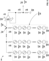
- FIG. 4 is a schematic diagram illustrating an example voltage reference circuit including an array of independent shunt voltage reference circuits in series.
- Circuit 200 in the example of FIG. 4 includes of an array of m parallel connected strings of series-connected bandgap references, each string having k references. Each string connects to the non-inverting input of amplifier AR1 202 through a respective averaging resistor, R1 221 - Rm 225.
- each resistor, R1 221 - Rm 225 has the same value so that the DC output of the network, VAVG 204, is the average of the m voltage references.
- VAVG VBG1 + VBG2 + ... + VBGm / m
- resistors R1 221 - Rm 225 may not contribute significantly to the output noise of the network, vn-avg 206, which is equal to the square root of the sum of each noise source squared, divided by m. (This is the same as the statistical average of the noise powers.)
- vn ⁇ avg SqrRoot vn1 2 + vn2 2 + ... + vnm 2 / m
- vn ⁇ avg vn * SqrRoot k / SqrRoot m
- vn ⁇ out Av * vn * SqrRoot k / SqrRoot m
- the bandgap voltage references, and the average noise voltage associated with each bandgap voltage reference may be approximately the same.
- “approximately the same” or “approximately equal” means that values are equal, within manufacturing and measurement tolerances. Process variation may mean that from wafer to wafer, or even for different locations on a same wafer, the values (voltage, current, resistance and other values) for different circuits may not be precisely equal to each other, however, within a circuit, such as circuit 200, the bandgap voltage references, and the average noise voltage associated with each bandgap voltage reference, may be approximately the same.
- bandgap references may be considered "approximately equal" when the output voltages are within 5% of each other.
- Other manufacturing processes may have values in the range of ⁇ 20%. This definition of approximately may similarly apply to other values in this disclosure, e.g., to resistor values, voltage drop and other values.
- the array 250 of parallel connected strings of series-connected bandgap references includes a first string connected to the Vavg 204 node through resistor R1 221.
- the first string, as well as the other strings of series-connected bandgap references, is the same as the series arrangement of k independent bandgap voltage references, 107 - 115, described above in relation to FIG. 3 , and may have the same or similar characteristics and functions.
- the first string includes bandgap voltage references VBG11 210, VBG21 214 through VBGk1 218, each connected in series such that the voltage value for each reference adds together at resistor R1 221.
- Each of bandgap voltage references VBG11 210, VBG21 214 through VBGk1 218 has an associated noise source vn11 208, vn21 212 through vnk1 216 in series with each bandgap voltage reference that may add an AC noise to the voltage output at R1 221.
- the second string through the mth string are arranged the same as the first string.
- the second string includes bandgap voltage references VBG12 240, VBG22 244 through VBGk2 248, each connected in series such that the voltage value for each reference adds together at resistor R1 222.
- Each of bandgap voltage references VBG12 240, VBG22 244 through VBGk2 248 has an associated noise source vn12 238, vn22 242 through vnk2 246 in series with each bandgap voltage reference.
- the mth string includes bandgap voltage references VBG1m 260, VBG2m 264 through VBGkm 268, each connected in series such that the voltage value for each reference adds together at resistor R1 225.
- Each of bandgap voltage references VBG1m 260, VBG2m 264 through VBGkm 268 has an associated noise source vnlm 258, vn2m 262 through vnkm 266 in series with each bandgap voltage reference.
- Each of the first string, second string and through mth string also connect to between ground, GND 220 and the respective averaging resistor to the non-inverting input of amplifier AR1 202.
- the output terminal of amplifier AR1 202 provides Vout 230, as well as vn-out 232 in the example of circuit 200.
- the output voltage, Vout 230 is fed back to the inverting input of AR1 202 through a resistor divider including resistors Rx 226 and Ry 228.
- a first terminal of Rx 226 connects to the output terminal of AR1 202, and the series arrangement of Rx 226 and Ry 228 connect the output terminal of AR1 202 to ground, GND 220.
- the node between Rx 226 and Ry 228 connects to the inverting terminal of AR1 202.
- the value of Rx 226 and Ry 228 may set the amplifier gain.
- AR1 202 also connects to Vdd 223 and to GND 220 and may have the same or similar functions and characteristics of amplifier AR1 102 described above in relation to FIG. 3 .
- circuit 200 reduces the noise for the same output voltage. As with the example of FIG. 3 , assuming each string consumes about same current as the amplifier, the total power consumption of circuit 200 is about five times IDD 224.
- Circuit 200 of FIG. 4 reduced the noise by the same amount as for circuit 950 of FIG. 2 , by using 16 independent bandgap voltage references.
- the power consumed by circuit 200 is significantly less: 5*IDD rather than 17*IDD (a 3.4x difference or about a 70.6% decrease), when compared to circuit 950.
- FIG. 5 is a schematic diagram of an example voltage reference circuit according to this disclosure that may be useful when the average voltage, V AVG 204, is larger than the desired output reference voltage, V OUT 330.
- VDD 323 is not much greater than the desired output voltage, VOUT 330.
- the VDD 323 voltage may be significantly greater (2x to 4x, or more) than the required output voltage, for example a 15V system that uses a 5V reference voltage. In such situations, the arrangement of circuit 300 may reduce noise even further than the previous circuits described above.
- Circuit 300 uses the same array 250 of parallel connected strings of series-connected bandgap references connected between ground, GND 220 and the respective averaging resistor, R1 321, R2 322 through Rm 325, to the non-inverting input of amplifier AR1 302.
- Array 250 has the same characteristics and functions as array 250 described above in relation to FIG. 4 .
- Vavg 204 and vn-avg 206 are also the same as described above in relation to FIG. 4 .
- Vavg 204 connects to the non-inverting input of amplifier AR1 302.
- Vout 330 In contrast to FIGS. 3 and 4 , Vout 330, and the associated noise output vn-out 332, is at the node between resistor divider Rx 326 and Ry 328.
- the output of amplifier AR1 302, Vx 327 connects to the inverting input of AR1 302.
- Vx 327 also connects to GND 220 through the series arrangement of Rx 326 and Ry 328.
- the value of voltage gain in this circuit is less than unity, 0 ⁇ Av ⁇ 1, which allows for higher k values and greater reductions in noise.
- VOUT 330 and vn-out 332 may be calculated as follows when the average value of all bandgap voltage references equals VBG and all bandgap voltage references have the same noise, vn, described above in relation to FIGS. 3 and 4 :
- equations 22 and 23 are essentially the same as those used to describe circuit 200 of FIG. 4 above, e.g., equations (13) and (20).
- a difference between FIGS. 2 and 3 is that the voltage gain is now less than or equal to unity, whereas before it was greater than or equal to unity.
- VBG silicon
- circuits of this disclosure allow the full use of the available supply voltage to minimize both output noise and power consumption.
- circuit 300 uses much less current: 2*IDD rather than 17*IDD (an 8.5x difference). Even if one accounts for an increased supply voltage for circuit 300, the circuit still consumes less than half of the power of circuit 950.
- FIG. 6 is a schematic diagram of an example voltage reference circuit according to this disclosure where the voltage divider is at the input to the amplifier.
- Circuit 400 in the example of FIG. 6 , is functionally the same as circuit 300 of FIG. 6 and follows the same equations. However, moving the voltage divider to the op amp input, allows the output, Vout 430, of amplifier AR1 402 to drive a larger load.
- circuit 400 may also use the same array 250 of parallel connected strings of series-connected bandgap references connected between ground, GND 220 and the respective averaging resistor, R1 421, R2 422 through Rm 425, to the non-inverting input of amplifier AR1 402.
- Array 250 has the same characteristics and functions as array 250 described above in relation to FIGS. 4 and 5 .
- the node for Av*Vavg 404 and Av*vn-avg 406 connects to the non-inverting input of amplifier AR1 402.
- RY 428 also connects the non-inverting input for AR1 402 to ground.
- the resistor value for RY 428 is not necessarily the same as the resistor value for R1 421 through Rm 425.
- RX e.g., RX 326 of FIG. 5
- RX R1/m, when all the averaging resistors are approximately equal
- VOUT 430 and vn-out 432 for this circuit are still defined by equations 22 and 23 described above for circuit 300. Note that amplifier AR1 may be omitted if it is not used to drive a large load in a specific application.
- This voltage reference noise reduction technique of any circuit of this disclosure may be implemented as a sub-circuit on larger integrated circuit (IC).
- the techniques of this disclosure may also be implemented as an array of discrete voltage reference ICs on a printed circuit board or larger assembly. Any silicon (Si) process could also be used to implement this technique. In fact, any number of non-silicon semi-conducting materials could be used to implement this technique.
- circuit topologies may be used to implement this technique.
- Circuit topologies from Widlar, Dobkin, Kuijk, Brokaw, Henry, Degrauwe, Annema, Friedman, Guenot, Werking, and many others may be used as the basic sub-circuit in the bandgap circuit array of this invention.
- the type of bandgap sub-circuit used is not material to this invention.
- any bandgap circuit topology may be used just as long it has a shunt configuration.
- a desirable shunt voltage reference may have a relatively small voltage compared to the output voltage.
- a shunt reference may have two terminals, e.g., OUT (high terminal) and GND (low terminal) and may be considered similar in concept to a Zener diode or simply an ideal voltage source that maintains a constant voltage between the OUT and GND terminals regardless of the current through the reference.
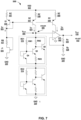
- FIG. 7 is a schematic diagram of an example voltage reference circuit including an array comprising a single string of independent bandgap voltage references, according to one or more techniques of this disclosure.
- Vsum 504 is the sum of BG1 510 and BG2 514, similar to the example of circuit 100 in FIG. 3 .
- Each of BG1 510 and BG2 514 may include an associated noise source (not shown in FIG. 7 ) as described above in relation to FIGS. 3-6 . Selecting Rx 526 and Ry 528 so that the gain of amplifier AR1 502 is one, then Vout 530 is based on the Vsum 504, and vn-out 532 is based on the sum of the noise sources.
- DC bias to BG1 510, BG2 514 and the output amplifier, AR1 502 is supplied by a junction FET, J1 545 through a set of current mirrors formed by Q1 546, Q2 547 and Q3 548.
- the current mirror transistors use emitter degeneration resistors, RZ 557, RZ 558 and RZ 559, to reduce noise introduced by the current mirror itself. These emitter degeneration resistors may not be needed for bipolar current mirrors; but degeneration resistors may be desirable for current mirrors using metal oxide semiconductor (MOS) transistors.
- Resistor RB 527 sets the bias current of the depletion mode junction field effect transistor (JFET), J1 545.
- J1 545 may be replaced by a metal-semiconductor field-effect transistor (MESFET).
- MESFET metal-semiconductor field-effect transistor
- Q1 546, Q2 547, Q3 548, RB 527 and J1 545 is just one possible example arrangement.
- a different type of current source circuit may supply current to Vsum 504.
- the arrangement of Q1 546, Q2 547 and Q3 548 may be replaced by a different circuit similar to the arrangement of Rb 527 and J1 545.
- Independent bandgap voltage reference BG1 510 is a Widlar reference including three NPN bipolar junction transistors (BJT).
- the collector of Q6 connects to Vsum 504 at the non-inverting input to AR1 502.
- the collector of Q6 connects to the collector of Q5 through resistor RW2 and to the collector of Q4 through resistor RW1.
- the collector of Q5 also connects to the base of Q6.
- the emitter of Q6 connects to the emitter of Q4, as well as through resistor RW3 to the emitter of Q5.
- the base of Q4 connects to the collector of Q4 and to the base of Q5.
- Voltage reference BG2 514 is arranged in the same way.
- Idd 524 runs from Vdd 523 through the series arrangement of RZ 557 and PNP BJT Q1 546.
- the emitter of Q1 546 connects to VDD 523 through RZ 557.
- the base of Q1 546 connects to the collector of Q1 546 and to the drain-source channel of JFET J1 545 through resistor RB 527.
- the gate of J1 545 connects to the collector of Q1 546.
- Idd 524 passes from Vdd 523 through resistor RZ 558, through PNP BJT Q2 547 and through BG1 510 and BG2 514 to GND 220.
- the emitter of Q2 547 connects to Vdd 523 through resistor RZ 558.
- the collector of Q2 547 is the Vsum 504, connected to BG1 510 and the non-inverting input of AR1 502.
- Idd 524 also feeds AR1 502 through resistor RZ 559, connected between VDD 523 and the emitter of Q3 548.
- the collector of Q3 548 connects to AR1 502.
- FIG. 8 is a schematic diagram of an example voltage reference circuit including an array comprising a merged arrangement of Widlar bandgap references. It is possible to merge two or more series connected bandgap cells into a single cell by connecting the individual components of the bandgap cell in series.
- the example of circuit 600 of FIG. 8 illustrates this merged arrangement for the two Widlar bandgap reference cells of circuit 500 described above in relation to FIG. 7 .
- each resistor in bandgap cell BG 610 has twice the value compared to the resistors in bandgap cell BG1 510 and BG2 514.
- circuit 600 illustrates an alternate arrangement for setting the bias current.
- a JFET may not be available in a given process, so the resistor, RB 628 may be used by itself to set the bias current (with a higher value of RB) at the expense of reduced power supply rejection.
- the bandgap voltage itself (Vsum 604) may be used to set the bias current.
- Circuit 600 illustrates the use of the constant VSUM voltage to set the bias current. Note that a diode D1 611, a resistor (RSU 625), and a third current mirror output are used to ensure that the bias circuit starts up properly.
- the value of RSU 625 may be much greater than the resistance value of RB 628.
- Circuit 600 includes a first current mirror carrying Idd 624 with the drain-source channel of PMOS transistor P6 646 connected to AR1 602 as well as to Vdd 623 through source degeneration resistor RZ 660.
- the output of AR1 602 provides Vout 630, and the associated noise output vn-out 632.
- the output of AR1 602 connects to ground through the series arrangement of resistor divider Rx 626 and Ry 628.
- the inverting input of AR1 602 connects to the node between Rx 626 and Ry 628.
- a second current mirror provides Idd 624 to the voltage reference circuit BG 610, with the drain-source channel of PMOS transistor P4 644 connected to BG610 as well as to Vdd 623 through source degeneration resistor RZ 659.
- the third current mirror provides current to start up circuit 600 with the drain-source channel of PMOS transistor MP1 640 connected to GND 220 through resistor RSU 625 as well as to Vdd 623 through source degeneration resistor RZ 657.
- the series arrangement of PMOS transistor MP2 642 and NMOS transistor MN8 648 connects to Vdd 623 through RZ 658 and to GND 220 through RB 628.
- the gate of MN8 648 connects to the Vsum 604 node.
- the gate of MP2 642 connects to the drains of MP2 642 and MP8 648 as well as to the gates of MP1 640, MP4 644 and MP6 646.
- the cathode of diode D1 connects to the drain of MP2 642 and the anode connects to the drain of MP1 640.
- the current source circuit arrangement of MP1 640, MP2 642, MP4 644 and MP6 646 may be replaced by a different current source circuit.
- the arrangement of FIG. 8 may be replaced by the arrangement of Q1 546, Q2 547 and Q3 548 along with J1 545 shown in FIG. 7 .
- the current source may be replaced by a different circuit similar to the arrangement of Rb 527 and J1 545.
- the circuit of FIG. 7 may use the current supply circuit shown in FIG. 8 , or some other equivalent circuit.
- FIG. 9 is a schematic diagram illustrating an example voltage reference circuit using an array of merged Brokaw voltage references, according to one or more techniques of this disclosure.
- Circuit 700 of FIG. 9 shows an example of four Brokaw cells merged together.
- circuit 700 may also include a start-up circuit and a pre-regulator circuit that are outside the scope of this disclosure (not shown in FIG. 9 ).
- Q1-Q3-Q5-Q7 are low current density devices and Q2-Q4-Q6-Q8 are high current density devices.
- the native output voltage of this circuit may be approximately 4.8V as shown in the trace of FIG. 10 , described below.
- circuit 700 may also be followed by an amplifier with a small amount of gain (not shown in FIG. 9 ) to provide a 5.0V DC output.
- Resistor R37 is on the base of transistor Q1 to provide base current compensation for curvature correction, as shown in the plot FIG. 10 below.
- Vdd 723 connects to the inverting input of AR1 702 and to the collector of NPN BJT Q1 through resistor R529. Vdd 723 also connect t through resistor R530 to the collector of NPN BJT Q2. The output of amplifier AR1 702 connects to the output Vout 730. T As with all the example circuits in this disclosure, in some examples, amplifier AR1 702 may be implemented as an operational transconductance amplifier.
- the series arrangement of Q1-Q3-Q5-Q7 connect to GND 720 through resistor R7 and resistor R8.
- the base of Q1 connects to Vout 730 through resistor R37.
- the base of Q3 connects to the emitter of Q1 and collector of Q3.
- the base of Q5 connects to the emitter of Q3 and collector of Q5.
- the base of Q7 connects to the emitter of Q5 and collector of Q7.
- the emitter of Q7 connects to resistor R7.
- the series arrangement of Q2-Q4-Q6-Q8 connects directly to the proportional to absolute temperature (PTAT) pin, PTAT 731.
- PTAT 731 connects to R8, as well as to the emitter of Q8.
- GND 720 may be a negative supply, as noted above.
- the base of Q2 connects to Vout 730.
- the base of Q4 connects to the emitter of Q2 and collector of Q4.
- the base of Q6 connects to the emitter of Q4 and collector of Q6.
- the base of Q8 connects to the emitter of Q6 and collector of Q8.
- FIG. 10 illustrates circuit performance of the output voltage over a wide temperature range.
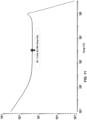
- FIG. 11 is a graph depicting the output noise performance of an example voltage reference circuit that includes an array of merged Brokaw voltage references. The performance described by the graph of FIG. 11 depict the noise performance of the example circuit 700, described above in relation to FIG. 9 .
- the measurements for the voltage reference circuit are based on a circuit fabricated using a silicon-on-insulator (SOI) process. However, any other silicon (Si) process could also be used to implement this technique. In fact, any number of non-silicon semi-conducting materials may also be used to implement this technique.
- SOI silicon-on-insulator
- the graph of FIG. 11 illustrates the output noise performance of circuit 700 over a frequency range. Above 100Hz, circuit 700 may exhibit a noise density of about 250nV/sqrt-Hz. When integrated over a 500kHz bandwidth, noise density amounts to a noise voltage of approximately 177 ⁇ Vrms. The example circuit 700 accomplished this level of noise with a total of 24 low gain NPN transistors operating at a total bias current of 120 ⁇ A occupying an area of only 162.6 ⁇ 98.6 ⁇ m.
- circuit 700 may result in a noise plot that shows an output noise floor of about 30nV/rt-Hz that occurs when resistor R8 is bypassed by an external capacitor to ground (e.g., on the PTAT 731 pin).
- resistor R8 When R8 is bypassed, the dominate source of noise is the output amplifier. Therefore, the circuit arrangement of this disclosure, described above in relation to FIGS. 3 - 11 may allow the full use of the available supply voltage to minimize both output noise and power consumption.
- Example 1 A circuit comprising an amplifier circuit comprising an output terminal configured to provide a voltage output; and an input terminal; a first shunt voltage reference circuit and a second shunt voltage reference circuit, wherein the first shunt voltage reference circuit includes a first low terminal and a first high terminal, wherein the second shut voltage reference circuit includes a second low terminal and second high terminal, wherein the first shunt voltage reference circuit connects in series with the second shunt voltage reference circuit such that the second high terminal connects to the first low terminal, wherein the first high terminal connects to the input terminal of the amplifier circuit.
- Example 2 The circuit of example 1, wherein the first shunt voltage reference circuit is a bandgap voltage reference circuit.
- Example 3 The circuit of any of examples 1 and 2, further comprising a third shunt voltage reference circuit including a third high terminal and a third low terminal, wherein the third high terminal connects to the second low terminal to connect the third shunt voltage reference circuit in series with the first shunt voltage reference circuit and the second shunt voltage reference circuit.
- Example 4 The circuit of any of examples 1 through 3, further comprising a third shunt voltage reference circuit and a fourth shunt voltage reference circuit, wherein the third shunt voltage reference circuit includes a third low terminal and a third high terminal, wherein the fourth shut voltage reference circuit includes a fourth low terminal and fourth high terminal, wherein the first shunt voltage reference circuit and the second shunt voltage reference circuit comprise a first string of series connected voltage reference circuits, wherein the third shunt voltage reference circuit connects in series with the fourth shunt voltage reference circuit such that the fourth high terminal connects to the third low terminal, to form a second string of series connected voltage reference circuits; wherein the third high terminal connects to the input terminal of the amplifier to form an array of parallel connected strings voltage reference circuits.
- the third shunt voltage reference circuit includes a third low terminal and a third high terminal
- the fourth shut voltage reference circuit includes a fourth low terminal and fourth high terminal
- the first shunt voltage reference circuit and the second shunt voltage reference circuit comprise a first string of series connected
- Example 5 The circuit of example 4, wherein each respective shunt voltage reference circuit has a voltage drop across each respective low terminal and high terminal, and wherein each of the respective voltage drops are approximately equal in magnitude.
- Example 6 The circuit of any of examples 4 and 5, wherein the first high terminal connects to the input terminal through a resistor.
- Example 7 The circuit of example 4, further comprising an amplifier feedback circuit including a resistor divider, wherein the voltage output from the output terminal of the amplifier circuit provides a reference voltage output, wherein the amplifier circuit comprises a second input terminal for an inverting input, and wherein a node between resistors of the resistor divider connects to the second input terminal.
- Example 8 The circuit of example 4, further comprising: an amplifier feedback circuit configured for unity gain; and a resistor divider connected to the output terminal of the amplifier circuit, wherein a node between resistors of the resistor divider provides a reference voltage output.
- Example 9 The circuit of example 4, further comprising: an amplifier feedback circuit configured for unity gain; and a resistor divider, wherein a node between resistors of the resistor divider connects to the input terminal.
- Example 10 The circuit of any of examples 1 through 10, further comprising an amplifier feedback circuit including a resistor divider, wherein the voltage output from the output terminal of the amplifier circuit provides a reference voltage output, wherein the amplifier circuit comprises a second input terminal for an inverting input, and wherein a node between resistors of the resistor divider connects to the second input terminal.
- an amplifier feedback circuit including a resistor divider, wherein the voltage output from the output terminal of the amplifier circuit provides a reference voltage output, wherein the amplifier circuit comprises a second input terminal for an inverting input, and wherein a node between resistors of the resistor divider connects to the second input terminal.
- Example 11 The circuit of any of examples 1 through 11, further comprising an amplifier feedback circuit configured for unity gain; and a resistor divider connected to the output terminal of the amplifier circuit, and wherein a node between resistors of the resistor divider provides a reference voltage output.
- Example 12 The circuit of any of examples 1 through 12, further comprising an amplifier feedback circuit configured for unity gain; and a resistor divider, and wherein a node between resistors of the resistor divider connects to the input terminal.
- Example 13 The circuit of any of examples 4 through 12, wherein the array of parallel connected strings voltage reference circuits are arranged as merged voltage reference circuits.
Landscapes
- Engineering & Computer Science (AREA)
- Physics & Mathematics (AREA)
- Microelectronics & Electronic Packaging (AREA)
- Electromagnetism (AREA)
- General Physics & Mathematics (AREA)
- Radar, Positioning & Navigation (AREA)
- Automation & Control Theory (AREA)
- Nonlinear Science (AREA)
- Power Engineering (AREA)
- Control Of Electrical Variables (AREA)
- Amplifiers (AREA)
Abstract
Voltage reference circuits configured to output reference voltages with a reduced noise on the output and reduced power consumption when compared to other arrangements of voltage reference circuits. The voltage reference circuit of this disclosure may stack two or more independent shunt voltage reference circuits in series to produce a summed voltage (Vsum), then amplify the summed voltage to output the desired reference voltage. The circuit of this disclosure may arrange the independent shunt voltage reference circuits to diminish any noise generated by each independent shunt voltage reference circuit in the summed voltage, for example as an array of independent shunt voltage reference circuits in series.
Description
- The disclosure relates to voltage reference circuits.
- Bandgap voltage reference circuits are part of many analog and mixed-signal integrated circuits. Bandgap voltage reference circuits may be arranged to provide a temperature independent output reference voltage.
- In general, the disclosure describes voltage reference circuits configured to output voltages of less than approximately twenty volts. Above this voltage one would commonly use either Zener or avalanche diodes. However, the techniques disclosed here could also be used with Zener and avalanche diodes to reduce the noise of higher voltage references and regulators. These techniques also reduce power consumption when compared to other arrangements of low noise voltage reference circuits. The voltage reference circuit of this disclosure may stack two or more independent shunt voltage reference circuits in series to produce a summed voltage (Vsum), then amplify the summed voltage to output the desired reference voltage. The circuit of this disclosure may arrange the independent shunt voltage reference circuits to diminish the noise generated by the overall voltage reference circuit. The arrangement of this disclosure also may diminish any noise in the amplified output of the summed voltage. Also, the arrangement of the independent shunt voltage reference circuits may consume less power when compared to other voltage reference circuit arrangements. In some applications, especially sensor applications, the noise of the bandgap voltage reference used can limit system performance. This disclosure presents several methods of reducing the noise of bandgap voltage references and regulators while minimizing the power and area consumed by these circuits.
- In one example, this disclosure describes a circuit comprising an amplifier circuit comprising an output terminal configured to provide a voltage output; and an input terminal; a first shunt voltage reference circuit and a second shunt voltage reference circuit, wherein the first shunt voltage reference circuit includes a first low terminal and a first high terminal, wherein the second shut voltage reference circuit includes a second low terminal and second high terminal, wherein the first shunt voltage reference circuit connects in series with the second shunt voltage reference circuit such that the second high terminal connects to the first low terminal, wherein the first high terminal connects to the input terminal of the amplifier circuit.
- The details of one or more examples of the disclosure are set forth in the accompanying drawings and the description below. Other features, objects, and advantages of the disclosure will be apparent from the description and drawings, and from the claims.
-
-
FIG. 1 is a schematic diagram illustrating an example voltage reference circuit with a single bandgap voltage reference and an associated noise source. -
FIG. 2 is a schematic diagram that illustrates one technique to reduce output noise for a bandgap voltage reference. -
FIG. 3 is a schematic diagram illustrating an example voltage reference circuit including independent shunt voltage reference circuits in series. -
FIG. 4 is a schematic diagram illustrating an example voltage reference circuit including an array of independent shunt voltage reference circuits in series. -
FIG. 5 is a schematic diagram of an example voltage reference circuit according to this disclosure that may be useful when the average bandgap voltage, VAVG is larger than the desired output reference voltage. -
FIG. 6 is a schematic diagram of an example voltage reference circuit according to this disclosure where the voltage divider is at the input to the amplifier. -
FIG. 7 is a schematic diagram of an example voltage reference circuit including an array comprising a single string of independent Widlar bandgap voltage references, according to one or more techniques of this disclosure. -
FIG. 8 is a schematic diagram of an example voltage reference circuit including an array comprising a merged arrangement of Widlar bandgap references. -
FIG. 9 is a schematic diagram illustrating an example voltage reference circuit using an array of merged Brokaw voltage references, according to one or more techniques of this disclosure. -
FIG. 10 is a graph of voltage versus temperature for an example bandgap reference circuit that includes an array of merged Brokaw voltage references. -
FIG. 11 is a graph depicting the output noise performance of an example voltage reference circuit that includes an array of merged Brokaw voltage references. - The disclosure describes voltage reference circuits configured to output reference voltages with a reduced noise on the output and reduced power consumption when compared to other arrangements of low noise voltage reference circuits. The voltage reference circuit of this disclosure may stack two or more independent shunt voltage reference circuits in series to produce a summed voltage (Vsum), then either amplify or attenuate the summed voltage, if needed, to output the desired reference voltage. In some examples the independent shunt voltage reference circuits may include temperature independent bandgap voltage reference circuits.
- Applications for which the voltage reference circuits of this disclosure may be desirable include Microelectromechanical system (MEMS) sensors, such as accelerometers, gyroscopes, and similar sensors. Because of the physics of the electrostatic fields involved, it may not be possible to reduce the bias voltages driving MEMS sensors, nor the sensor output voltages, even when the physical dimensions of the sensor may be reduced. Therefore, most MEMS sensors may operate at voltages of about 5V to 20V and may continue to do so for the foreseeable future. Other example applications may also include quantum computing where similar voltages are required and low noise is desirable for maintaining the lifetime of the "qubits" at the heart of the computer.
- In sensor circuits, the noise of the voltage references supporting the sensor circuits may limit the sensitivity and/or precision of the sensor. In MEMS sensors, for example, noise may reduce sensor performance in two ways. First, by adding noise to a bias reference (either AC or DC) used by the sensor, which is then coupled to the sensor output. Second, by adding noise to the reference used by the analog-to-digital converter (ADC) used to capture the sensor signal output, small errors may appear in the converted digital quantity which may also limit sensitivity and resolution.
- The circuit of this disclosure address these challenges and may arrange the independent shunt voltage reference circuits to diminish any noise generated by each independent shunt voltage reference circuit in the summed voltage. Therefore, the arrangement of this disclosure also may diminish any noise in the amplified output of the summed voltage.
- Some examples of techniques to reduce reference noise voltages generally require large current consumption so that these voltage reference circuits consume more power than the rest of the MEMS sensor circuit. In contrast, the arrangement of the independent shunt voltage reference circuits of this disclosure may consume less power when compared to these other voltage reference circuit arrangements.
-
FIG. 1 is a schematic diagram illustrating an example voltage reference circuit with a single bandgap voltage reference and an associated noise source. In the example ofcircuit 900 ofFIG. 1 , VBG 910 represents the temperature stable DC voltage supplied by the bandgap voltage reference andvn 908 represents the equivalent AC noise voltage of this reference. These voltages are then amplified by ideal noiseless op amp,AR1 902, which provides a positive closed-loop gain of Av = (1+RX/RY) set byresistors Vout 930, and an equivalent output noise voltage, vn-out 932, as specified below.

- These equations assume that the noise contributions of the amplifier and the resistors are insignificant. To provide a 5V output voltage (Vout 930) from a 1.25V bandgap voltage reference (VBG 910) having a noise voltage (vn 908), for example, of 10uVrms,
circuit 900 uses amplification. Setting the value of RX=3*RY produces a voltage gain of four (Av = 1+3 = 4) to achieve the desired output voltage of 5V However,vn 908 is also amplified by Av = 4 so that vn-out 932 becomes 40uVrms. -
FIG. 2 is a schematic diagram that illustrates one technique to reduce output noise for a bandgap voltage reference. In the example ofcircuit 950, the outputs of several independent bandgap voltage references may be combined. In this circuit, there are an integer number of bandgap voltage references (m) connect together by m resistors. Each ofresistors R1 921, R2 922 throughRm 925 has the same value so that the DC output of the network of bandgap references,VAVG 904, is the average of the m voltage references, e.g.,
- As also described below for
FIG. 3 , when all voltage references have roughly the same value (or at least the same average value), VBG, equation 3 reduces to the following equation and the output voltage is the same as before.

- By keeping the values of the m resistors low enough, the resistors do not contribute significantly to the output noise of the network, vn-
avg 906, which is equal to the square root of the sum of each noise source squared, divided by m. (This is the same as the statistical average of the noise powers.)
- As noted above, when all voltage references have the same average noise voltage, vn, this reduces to the following and the output noise voltage is reduced accordingly.


- When compared to
circuit 900 ofFIG. 1 , using four independent bandgap voltage references may reduce the output noise by a factor of 1/2, e.g., to 20µVrms. In another example, setting m = 16, and using 16 independent bandgap voltage references, the output noise may be reduced by a factor of 1/4 to 10µVrms. This counteracts the noise gain of the amplifier, Av=4. However, adding additional voltage references in this manner may significantly increase overall power consumption. This is because each bandgap voltage reference would have about the same DC current consumption as foramplifier AR1 952, e.g.,IDD 954. Staying with this numerical example,circuit 900 may have an overall current consumption of 2*IDD, whilecircuit 950 may have a current consumption of either 5*IDD or 17*IDD in the examples where m equals 4 and 16 respectively. In other words, these two examples may cause either a 2.5x (5/2) or an 8.5x (17/2) increase in power dissipation if it is assumed that all circuits work from the same supply voltage,VDD 923. -
FIG. 3 is a schematic diagram illustrating an example voltage reference circuit including independent shunt voltage reference circuits in series.Circuit 900 ofFIG. 1 is similar, but with k= 1. In the example ofcircuit 100, VBG, e.g.,VBG1 110, represents a temperature stable DC voltage supplied by the bandgap voltage reference and vn, e.g., vn1 108, represents the equivalent AC noise voltage of this reference. The series arrangement includes an integer number, k, of independent bandgap voltage references, 107 - 115, are connected in series. The circuit arrangement results in the DC and noise voltages being summed at the non-inverting input toamplifier AR1 102, to provideVSUM 104 and vnsum 106 per the equations below:

- Ideal noiseless op amp,
AR1 102, which provides a positive closed-loop gain of Av = (1+RX/RY) amplifies the two summed voltages to provide the DC output voltage, VOUT, and equivalent output noise voltage, vnout, per the following equations:

- In these equations, it is assumed that the noise contributions of the amplifier and the resistors are insignificant.
- In more detail, the output terminal of
amplifier AR1 102 providesVout 130, as well as vn-out 132 in the example ofcircuit 100. The output voltage,Vout 130 is fed back to the inverting input ofAR1 102 through a resistor divider includingresistors Rx 126 andRy 128. A first terminal ofRx 126 connects to the output terminal ofAR1 102, and the series arrangement ofRx 126 andRy 128 connect the output terminal ofAR1 102 to ground,GND 120. The node betweenRx 126 andRy 128 connects to the inverting terminal ofAR1 102. Note that in this disclosure,GND 120 may be, for example, a circuit ground, a system ground, a layer in an integrated circuit, or some reference voltage, e.g., a voltage source opposite in polarity from Vdd 123, butGND 120 will be referred to asGND 120 to simplify the description of the circuits of this disclosure. - In some examples,
amplifier AR1 102 may be implemented as an operational transconductance amplifier (OTA).AR1 102 also connects to Vdd 123 and toGND 120. The series arrangement of independent bandgapvoltage reference circuits Vsum 104. The voltage reference circuits in the example ofcircuit 100 are described as bandgap voltage references, however, the voltage reference circuit of this disclosure may also be implemented using any shunt voltage reference. - In the example of
circuit 100, independentbandgap voltage reference 107 connects to the non-inverting input ofAR1 102. Independentbandgap voltage reference 107 includesVBG1 110, the bandgap voltage reference, and an associated AC noise source vn1 108. In the example ofcircuit 100, the positive terminal ofVB1 110 connects to the positive terminal ofAR1 102 through noise source vn1 108. However, in other examples,VBG1 110 and vn1 108 may connect in either series order. Independentbandgap voltage reference 109, which includesVBG2 114 andvn2 112, connects to independentbandgap voltage reference 107, as well as to the other k voltage references in the series down to independentbandgap voltage reference 115, which includesVBGk 118 andvnk 116. - To simplify the description, assume all bandgap voltage references of
circuit 100 have the same DC voltage, VBG, and the same noise voltage, vn. Then equations (9) - (12) may be simplified as follows:

- Note that
circuit 100 has no averaging resistors that could possibly increase the output noise level if the resistance values were large. The series arrangement that results inVsum 104 means the gain foramplifier AR1 102 may only be enough to provideVout 130 to be at the desired magnitude. In some examples the maximum value of gain needed by this circuit is as follows, where k is any positive integer.
- Because any gain in
AR1 102 also amplifies the noise vn-sum 106, then a voltage reference circuit with a reduced amplifier gain may result in reduced noise vn-out 132, when compared to circuits with higher gain amplifiers. The value ofRx 126 andRy 128 may set the gain, Av foramplifier AR1 102. For example, setting the value of RX=3*RY produces a voltage gain of four (Av = 1+3 = 4). However, vn is also amplified by Av=4. Forcircuit 100, if more gain is needed then k may be increased by adding another series bandgap voltage reference. In principle,circuit 100 may produce any arbitrary output voltage,VOUT 130, greater than the magnitude of voltage output from each independent bandgap voltage references, e.g., VBG. In some examples, such precision for a voltage reference may not be necessary and the amplifier circuit,AR1 102, may be omitted altogether (not shown inFIG. 3 ). - The utility of
circuit 100 may be shown by the following numerical example. Consider a goal of providing a 5V voltage reference output using bandgap references with each output voltage VBG = 1.25V and each having vn = 10uVrms of noise. By placing four bandgap references in series (k=4), the output voltage becomes 5V (VOUT = 1 * 4 * 1.25V) when Av=1, and output noise voltage becomes 20uVrms (vnout = 1 * 2 * 10uVrms), by applying equations (13) and (14). The stacked (series) arrangement reduces the noise contribution at vn-out 132 by less than a simple sum of the noise voltage contributions (Vn1 108,vn2 112 ... vnk 116). - Also, in
circuit 100, all four shunt bandgap voltage references share the same supply current. Assume that the current to the series arrangement (string) of independent bandgap voltage references is equal to the op amp supply current,IDD 124. Therefore, the total supply current tocircuit 100 becomes 2*IDD which is significantly less than the supply current needed in other examples. In essence,circuit 100 may be desirable over other examples because the required gain decreases faster (1/k) with the ratio of VOUT/VBG than the noise increases (square root of k). Thus, the circuit ofFIG. 3 , with the series combination of voltage reference circuits, provides the same 5V reference ascircuit 900, but with reduced noise. -
FIG. 4 is a schematic diagram illustrating an example voltage reference circuit including an array of independent shunt voltage reference circuits in series.Circuit 200 in the example ofFIG. 4 includes of an array of m parallel connected strings of series-connected bandgap references, each string having k references. Each string connects to the non-inverting input ofamplifier AR1 202 through a respective averaging resistor, R1 221 -Rm 225. In the example ofcircuit 200, each resistor, R1 221 -Rm 225, has the same value so that the DC output of the network,VAVG 204, is the average of the m voltage references.
- As described above in relation to
FIG. 1 , if these bandgap voltage references all have the same DC value, VBG, then the DC output voltage is the same as equation 13 described above in relation toFIG. 3 :
- By selecting low enough values for the m resistors, resistors R1 221 -
Rm 225, they may not contribute significantly to the output noise of the network, vn-avg 206, which is equal to the square root of the sum of each noise source squared, divided by m. (This is the same as the statistical average of the noise powers.)
- If all voltage references have the same average noise voltage, vn, the noise equation may be simplified to the following and the output noise voltage, vn-out 232 is reduced accordingly.


- In the example of
circuit 200 implemented in an integrated circuit, then for a given manufacturing process run, the bandgap voltage references, and the average noise voltage associated with each bandgap voltage reference, may be approximately the same. In this disclosure, "approximately the same" or "approximately equal" means that values are equal, within manufacturing and measurement tolerances. Process variation may mean that from wafer to wafer, or even for different locations on a same wafer, the values (voltage, current, resistance and other values) for different circuits may not be precisely equal to each other, however, within a circuit, such ascircuit 200, the bandgap voltage references, and the average noise voltage associated with each bandgap voltage reference, may be approximately the same. As one example, for the silicon-on-insulator (SOI) process, bandgap references may be considered "approximately equal" when the output voltages are within 5% of each other. Other manufacturing processes may have values in the range of ±20%. This definition of approximately may similarly apply to other values in this disclosure, e.g., to resistor values, voltage drop and other values. - The
array 250 of parallel connected strings of series-connected bandgap references, includes a first string connected to theVavg 204 node throughresistor R1 221. The first string, as well as the other strings of series-connected bandgap references, is the same as the series arrangement of k independent bandgap voltage references, 107 - 115, described above in relation toFIG. 3 , and may have the same or similar characteristics and functions. The first string includes bandgap voltage referencesVBG11 210,VBG21 214 throughVBGk1 218, each connected in series such that the voltage value for each reference adds together atresistor R1 221. Each of bandgap voltage referencesVBG11 210,VBG21 214 throughVBGk1 218 has an associatednoise source vn11 208, vn21 212 throughvnk1 216 in series with each bandgap voltage reference that may add an AC noise to the voltage output atR1 221. - Similarly, the second string through the mth string are arranged the same as the first string. The second string includes bandgap voltage references VBG12 240,
VBG22 244 throughVBGk2 248, each connected in series such that the voltage value for each reference adds together at resistor R1 222. Each of bandgap voltage references VBG12 240,VBG22 244 throughVBGk2 248 has an associatednoise source vn12 238,vn22 242 throughvnk2 246 in series with each bandgap voltage reference. The mth string includes bandgap voltage referencesVBG1m 260,VBG2m 264 throughVBGkm 268, each connected in series such that the voltage value for each reference adds together atresistor R1 225. Each of bandgap voltage referencesVBG1m 260,VBG2m 264 throughVBGkm 268 has an associatednoise source vnlm 258,vn2m 262 throughvnkm 266 in series with each bandgap voltage reference. Each of the first string, second string and through mth string also connect to between ground,GND 220 and the respective averaging resistor to the non-inverting input ofamplifier AR1 202. - As described above in relation to
FIG. 3 , the output terminal ofamplifier AR1 202 provides Vout 230, as well as vn-out 232 in the example ofcircuit 200. The output voltage, Vout 230 is fed back to the inverting input ofAR1 202 through a resistor divider includingresistors Rx 226 andRy 228. A first terminal ofRx 226 connects to the output terminal ofAR1 202, and the series arrangement ofRx 226 andRy 228 connect the output terminal ofAR1 202 to ground,GND 220. The node betweenRx 226 andRy 228 connects to the inverting terminal ofAR1 202. As withcircuit 100, the value ofRx 226 andRy 228 may set the amplifier gain.AR1 202 also connects toVdd 223 and toGND 220 and may have the same or similar functions and characteristics ofamplifier AR1 102 described above in relation toFIG. 3 . - Now apply a similar numerical example as for
FIG. 3 for a voltage reference circuit using the arrangement ofcircuit 200 configured for a 5V output using 1.25V references (VBG). By placing four bandgap references in series (k = 4), the output voltage again becomes 5V (VOUT = 1 * 4 * 1.25V) when Av = 1. Then, by also averaging four of these strings together (m=4), the output noise voltage becomes 10uVrms (e.g., vnout = 1 * (2/2) * 10uVrms). When compared tocircuit 100 ofFIG. 3 ,circuit 200 reduces the noise for the same output voltage. As with the example ofFIG. 3 , assuming each string consumes about same current as the amplifier, the total power consumption ofcircuit 200 is about fivetimes IDD 224. -
Circuit 200 ofFIG. 4 reduced the noise by the same amount as forcircuit 950 ofFIG. 2 , by using 16 independent bandgap voltage references. However, with the arrangement ofFIG. 4 , e.g., the array of m parallel connected strings of series-connected bandgap references, each string having k references, the power consumed bycircuit 200 is significantly less: 5*IDD rather than 17*IDD (a 3.4x difference or about a 70.6% decrease), when compared tocircuit 950. -
FIG. 5 is a schematic diagram of an example voltage reference circuit according to this disclosure that may be useful when the average voltage,V AVG 204, is larger than the desired output reference voltage,V OUT 330. Often,VDD 323, is not much greater than the desired output voltage,VOUT 330. However, in some applications, theVDD 323 voltage may be significantly greater (2x to 4x, or more) than the required output voltage, for example a 15V system that uses a 5V reference voltage. In such situations, the arrangement ofcircuit 300 may reduce noise even further than the previous circuits described above. -
Circuit 300 uses thesame array 250 of parallel connected strings of series-connected bandgap references connected between ground,GND 220 and the respective averaging resistor,R1 321, R2 322 through Rm 325, to the non-inverting input ofamplifier AR1 302.Array 250 has the same characteristics and functions asarray 250 described above in relation toFIG. 4 .Vavg 204 and vn-avg 206 are also the same as described above in relation toFIG. 4 .Vavg 204 connects to the non-inverting input ofamplifier AR1 302. - In contrast to
FIGS. 3 and4 ,Vout 330, and the associated noise output vn-out 332, is at the node betweenresistor divider Rx 326 andRy 328. The output ofamplifier AR1 302,Vx 327 connects to the inverting input ofAR1 302.Vx 327 also connects to GND 220 through the series arrangement ofRx 326 andRy 328. - As shown in
FIG. 5 , the value of voltage gain in this circuit is less than unity, 0 < Av < 1, which allows for higher k values and greater reductions in noise. InFIG. 5 , theamplifier AR1 302 is configured as a unity gain buffer and its output,VX 327, is divided by the RX-RY resistive divider so the voltage gain follows the expression below:
- Accordingly,
VOUT 330 and vn-out 332 may be calculated as follows when the average value of all bandgap voltage references equals VBG and all bandgap voltage references have the same noise, vn, described above in relation toFIGS. 3 and4 :

- Note that
equations 22 and 23 are essentially the same as those used to describecircuit 200 ofFIG. 4 above, e.g., equations (13) and (20). A difference betweenFIGS. 2 and3 is that the voltage gain is now less than or equal to unity, whereas before it was greater than or equal to unity. - A numerical example of a desired 5V reference voltage circuit implemented with the output arrangement of
FIG. 5 and m=1, with sixteen bandgap voltage references in series, e.g., k=16 would result in a single string, or row, of band gap references, similar to the arrangement ofcircuit 100 shown inFIG. 3 . As described above, assuming VBG for silicon, VBG=1.25V, such an arrangement may produce an output ofVX 327 = 20V, while consuming 2*IDD, e.g., about twiceIdd 324. To produce the desired 5V output,VOUT 330 = 5V, the voltage gain, Av, may be set to ¼, accomplished by setting RX=3*RY. For an example in which the noise sources output an average vn = 10 microvolts rms (µVrms), the output noise is 10µVrms according to:
- In another example, where k = 8, m = 2, VBG = 1.25V, VOUT = 5 V, VDD = 12V, and vn=10uVrms. This circuit arrangement of
circuit 300 still contains 16 bandgap voltage references. The output ofAR1 302VX 327 is 10V, so to setVout 330 to five volts, then Av = ½, which would produce 10µVrms of output noise, vn-out 332 according to:
-
Circuit 300, with m = 2 would consume 3*IDD and the relative power consumed is only 6*PX, according to:
- The utility of the circuits of this disclosure is that the circuits allow the full use of the available supply voltage to minimize both output noise and power consumption.
- The numerical
example using circuit 300 also produced the same reduced amount of output noise produced bycircuit 950 with m=16. However,circuit 300 uses much less current: 2*IDD rather than 17*IDD (an 8.5x difference). Even if one accounts for an increased supply voltage forcircuit 300, the circuit still consumes less than half of the power ofcircuit 950. For the sake of comparison, assume thatVDD 923 = 6V forcircuit 950 and thatVDD 323 = 24V forcircuit 300. Therefore, to calculateVDD 323 = 4*VDD 923 and the corresponding power consumptions as follows.

-
FIG. 6 is a schematic diagram of an example voltage reference circuit according to this disclosure where the voltage divider is at the input to the amplifier.Circuit 400, in the example ofFIG. 6 , is functionally the same ascircuit 300 ofFIG. 6 and follows the same equations. However, moving the voltage divider to the op amp input, allows the output,Vout 430, ofamplifier AR1 402 to drive a larger load. - Similar to
circuit 300 described above in relation toFIG. 5 ,circuit 400 may also use thesame array 250 of parallel connected strings of series-connected bandgap references connected between ground,GND 220 and the respective averaging resistor,R1 421,R2 422 throughRm 425, to the non-inverting input ofamplifier AR1 402.Array 250 has the same characteristics and functions asarray 250 described above in relation toFIGS. 4 and5 . The node for Av*Vavg 404 and Av*vn-avg 406 connects to the non-inverting input ofamplifier AR1 402. RY 428 also connects the non-inverting input forAR1 402 to ground. The resistor value for RY 428 is not necessarily the same as the resistor value forR1 421 throughRm 425. - By defining RX, e.g.,
RX 326 ofFIG. 5 , to be the parallel combination of R1-Rm (i.e., RX = R1/m, when all the averaging resistors are approximately equal) it is still possible to use equation 21, described above forFIG. 5 , to determine voltage gain, Av.

-
VOUT 430 and vn-out 432 for this circuit are still defined byequations 22 and 23 described above forcircuit 300. Note that amplifier AR1 may be omitted if it is not used to drive a large load in a specific application. - This voltage reference noise reduction technique of any circuit of this disclosure may be implemented as a sub-circuit on larger integrated circuit (IC). However, the techniques of this disclosure may also be implemented as an array of discrete voltage reference ICs on a printed circuit board or larger assembly. Any silicon (Si) process could also be used to implement this technique. In fact, any number of non-silicon semi-conducting materials could be used to implement this technique.
- In addition, a large number of circuit topologies may be used to implement this technique. Circuit topologies from Widlar, Dobkin, Kuijk, Brokaw, Henry, Degrauwe, Annema, Friedman, Guenot, Werking, and many others may be used as the basic sub-circuit in the bandgap circuit array of this invention. The type of bandgap sub-circuit used is not material to this invention. As described above in relation to
FIG. 3 , any bandgap circuit topology may be used just as long it has a shunt configuration. In some examples, a desirable shunt voltage reference may have a relatively small voltage compared to the output voltage. A shunt reference may have two terminals, e.g., OUT (high terminal) and GND (low terminal) and may be considered similar in concept to a Zener diode or simply an ideal voltage source that maintains a constant voltage between the OUT and GND terminals regardless of the current through the reference. -
FIG. 7 is a schematic diagram of an example voltage reference circuit including an array comprising a single string of independent bandgap voltage references, according to one or more techniques of this disclosure.Circuit 500 in the example ofFIG. 7 uses the Widlar design as the basic bandgap cell with k=2 and m=1 so that VOUT=2*VBG. In other words,Vsum 504 is the sum ofBG1 510 andBG2 514, similar to the example ofcircuit 100 inFIG. 3 . Each ofBG1 510 andBG2 514 may include an associated noise source (not shown inFIG. 7 ) as described above in relation toFIGS. 3-6 . SelectingRx 526 andRy 528 so that the gain ofamplifier AR1 502 is one, thenVout 530 is based on theVsum 504, and vn-out 532 is based on the sum of the noise sources. - DC bias to BG1 510,
BG2 514 and the output amplifier,AR1 502 is supplied by a junction FET,J1 545 through a set of current mirrors formed byQ1 546,Q2 547 andQ3 548. The current mirror transistors use emitter degeneration resistors,RZ 557,RZ 558 andRZ 559, to reduce noise introduced by the current mirror itself. These emitter degeneration resistors may not be needed for bipolar current mirrors; but degeneration resistors may be desirable for current mirrors using metal oxide semiconductor (MOS) transistors.Resistor RB 527 sets the bias current of the depletion mode junction field effect transistor (JFET),J1 545. In someexamples J1 545 may be replaced by a metal-semiconductor field-effect transistor (MESFET). - The example arrangement of
Q1 546,Q2 547,Q3 548,RB 527 andJ1 545 is just one possible example arrangement. In other examples, a different type of current source circuit may supply current toVsum 504. For example, the arrangement ofQ1 546,Q2 547 andQ3 548 may be replaced by a different circuit similar to the arrangement ofRb 527 andJ1 545. - Independent bandgap
voltage reference BG1 510, in the example ofFIG. 7 , is a Widlar reference including three NPN bipolar junction transistors (BJT). The collector of Q6 connects toVsum 504 at the non-inverting input toAR1 502. The collector of Q6 connects to the collector of Q5 through resistor RW2 and to the collector of Q4 through resistor RW1. The collector of Q5 also connects to the base of Q6. The emitter of Q6 connects to the emitter of Q4, as well as through resistor RW3 to the emitter of Q5. The base of Q4 connects to the collector of Q4 and to the base of Q5.Voltage reference BG2 514 is arranged in the same way.Idd 524 runs fromVdd 523 through the series arrangement ofRZ 557 andPNP BJT Q1 546. The emitter ofQ1 546 connects toVDD 523 throughRZ 557. The base ofQ1 546 connects to the collector ofQ1 546 and to the drain-source channel ofJFET J1 545 throughresistor RB 527. The gate ofJ1 545 connects to the collector ofQ1 546. -
Idd 524 passes fromVdd 523 throughresistor RZ 558, throughPNP BJT Q2 547 and throughBG1 510 andBG2 514 toGND 220. The emitter ofQ2 547 connects toVdd 523 throughresistor RZ 558. The collector ofQ2 547 is theVsum 504, connected to BG1 510 and the non-inverting input ofAR1 502.Idd 524 also feedsAR1 502 throughresistor RZ 559, connected betweenVDD 523 and the emitter ofQ3 548. The collector ofQ3 548 connects toAR1 502. -
FIG. 8 is a schematic diagram of an example voltage reference circuit including an array comprising a merged arrangement of Widlar bandgap references. It is possible to merge two or more series connected bandgap cells into a single cell by connecting the individual components of the bandgap cell in series. The example ofcircuit 600 ofFIG. 8 illustrates this merged arrangement for the two Widlar bandgap reference cells ofcircuit 500 described above in relation toFIG. 7 . Note that each resistor inbandgap cell BG 610 has twice the value compared to the resistors inbandgap cell BG1 510 andBG2 514. Both ofcircuits FIGS. 5 and6 produce the same output voltage, VOUT = 2*VBG, and output noise level, vnout = SqrRoot(2)*vn, as described above in relation toFIG. 7 . - Also, when compared to
circuit 500 ofFIG. 7 ,circuit 600 illustrates an alternate arrangement for setting the bias current. In some examples, a JFET may not be available in a given process, so the resistor,RB 628 may be used by itself to set the bias current (with a higher value of RB) at the expense of reduced power supply rejection. In other examples, when JFETs are not available, the bandgap voltage itself (Vsum 604) may be used to set the bias current. UsingVsum 604 has the advantage of providing a stable bias current and good power supply rejection but may be more complex and use a start-up circuit to prevent the circuit from locking up when the circuit is in the VSUM=0 and IDD=0 state, e.g., at low temperatures.Circuit 600 illustrates the use of the constant VSUM voltage to set the bias current. Note that adiode D1 611, a resistor (RSU 625), and a third current mirror output are used to ensure that the bias circuit starts up properly. The value ofRSU 625 may be much greater than the resistance value ofRB 628. -
Circuit 600 includes a first currentmirror carrying Idd 624 with the drain-source channel ofPMOS transistor P6 646 connected toAR1 602 as well as toVdd 623 through sourcedegeneration resistor RZ 660. The output ofAR1 602 providesVout 630, and the associated noise output vn-out 632. The output ofAR1 602 connects to ground through the series arrangement ofresistor divider Rx 626 andRy 628. The inverting input ofAR1 602 connects to the node betweenRx 626 andRy 628. - A second current mirror provides
Idd 624 to the voltagereference circuit BG 610, with the drain-source channel ofPMOS transistor P4 644 connected to BG610 as well as toVdd 623 through sourcedegeneration resistor RZ 659. The third current mirror provides current to start upcircuit 600 with the drain-source channel ofPMOS transistor MP1 640 connected toGND 220 throughresistor RSU 625 as well as toVdd 623 through sourcedegeneration resistor RZ 657. The series arrangement ofPMOS transistor MP2 642 andNMOS transistor MN8 648 connects toVdd 623 throughRZ 658 and toGND 220 throughRB 628. The gate ofMN8 648 connects to theVsum 604 node. The gate ofMP2 642 connects to the drains ofMP2 642 andMP8 648 as well as to the gates ofMP1 640,MP4 644 andMP6 646. The cathode of diode D1 connects to the drain ofMP2 642 and the anode connects to the drain ofMP1 640. - As described above in relation to
FIG. 7 , the current source circuit arrangement ofMP1 640,MP2 642,MP4 644 andMP6 646 may be replaced by a different current source circuit. As one example, the arrangement ofFIG. 8 may be replaced by the arrangement ofQ1 546,Q2 547 andQ3 548 along withJ1 545 shown inFIG. 7 . In other examples, the current source may be replaced by a different circuit similar to the arrangement ofRb 527 andJ1 545. Similarly, the circuit ofFIG. 7 may use the current supply circuit shown inFIG. 8 , or some other equivalent circuit. -
FIG. 9 is a schematic diagram illustrating an example voltage reference circuit using an array of merged Brokaw voltage references, according to one or more techniques of this disclosure. In principle, any basic bandgap cell may be merged in this manner.Circuit 700 ofFIG. 9 shows an example of four Brokaw cells merged together. In some examples,circuit 700 may also include a start-up circuit and a pre-regulator circuit that are outside the scope of this disclosure (not shown inFIG. 9 ). Q1-Q3-Q5-Q7 are low current density devices and Q2-Q4-Q6-Q8 are high current density devices. In some examples, the native output voltage of this circuit may be approximately 4.8V as shown in the trace ofFIG. 10 , described below. In some examples,circuit 700 may also be followed by an amplifier with a small amount of gain (not shown inFIG. 9 ) to provide a 5.0V DC output. Resistor R37 is on the base of transistor Q1 to provide base current compensation for curvature correction, as shown in the plotFIG. 10 below. - In more detail, Vdd 723 connects to the inverting input of AR1 702 and to the collector of NPN BJT Q1 through resistor R529. Vdd 723 also connect t through resistor R530 to the collector of NPN BJT Q2. The output of amplifier AR1 702 connects to the
output Vout 730. T As with all the example circuits in this disclosure, in some examples, amplifier AR1 702 may be implemented as an operational transconductance amplifier. - The series arrangement of Q1-Q3-Q5-Q7 connect to GND 720 through resistor R7 and resistor R8. The base of Q1 connects to Vout 730 through resistor R37. The base of Q3 connects to the emitter of Q1 and collector of Q3. The base of Q5 connects to the emitter of Q3 and collector of Q5. The base of Q7 connects to the emitter of Q5 and collector of Q7. The emitter of Q7 connects to resistor R7.
- The series arrangement of Q2-Q4-Q6-Q8 connects directly to the proportional to absolute temperature (PTAT) pin,
PTAT 731.PTAT 731 connects to R8, as well as to the emitter of Q8. In someexamples GND 720 may be a negative supply, as noted above. The base of Q2 connects toVout 730. The base of Q4 connects to the emitter of Q2 and collector of Q4. The base of Q6 connects to the emitter of Q4 and collector of Q6. The base of Q8 connects to the emitter of Q6 and collector of Q8. -
FIG. 10 illustrates circuit performance of the output voltage over a wide temperature range.FIG. 11 is a graph depicting the output noise performance of an example voltage reference circuit that includes an array of merged Brokaw voltage references. The performance described by the graph ofFIG. 11 depict the noise performance of theexample circuit 700, described above in relation toFIG. 9 . The measurements for the voltage reference circuit are based on a circuit fabricated using a silicon-on-insulator (SOI) process. However, any other silicon (Si) process could also be used to implement this technique. In fact, any number of non-silicon semi-conducting materials may also be used to implement this technique. - The graph of
FIG. 11 illustrates the output noise performance ofcircuit 700 over a frequency range. Above 100Hz,circuit 700 may exhibit a noise density of about 250nV/sqrt-Hz. When integrated over a 500kHz bandwidth, noise density amounts to a noise voltage of approximately 177µVrms. Theexample circuit 700 accomplished this level of noise with a total of 24 low gain NPN transistors operating at a total bias current of 120µA occupying an area of only 162.6 × 98.6 µm. - The noise of this circuit is not limited by either the bandgap amplifier, AR1 702 in
FIG. 9 , or the output amplifier (not shown inFIG. 9 ). Though not shown inFIG. 11 ,circuit 700 may result in a noise plot that shows an output noise floor of about 30nV/rt-Hz that occurs when resistor R8 is bypassed by an external capacitor to ground (e.g., on thePTAT 731 pin). When R8 is bypassed, the dominate source of noise is the output amplifier. Therefore, the circuit arrangement of this disclosure, described above in relation toFIGS. 3 - 11 may allow the full use of the available supply voltage to minimize both output noise and power consumption. - The techniques of this disclosure may also be described in the following examples.
- Example 1: A circuit comprising an amplifier circuit comprising an output terminal configured to provide a voltage output; and an input terminal; a first shunt voltage reference circuit and a second shunt voltage reference circuit, wherein the first shunt voltage reference circuit includes a first low terminal and a first high terminal, wherein the second shut voltage reference circuit includes a second low terminal and second high terminal, wherein the first shunt voltage reference circuit connects in series with the second shunt voltage reference circuit such that the second high terminal connects to the first low terminal, wherein the first high terminal connects to the input terminal of the amplifier circuit.
- Example 2: The circuit of example 1, wherein the first shunt voltage reference circuit is a bandgap voltage reference circuit.
- Example 3: The circuit of any of examples 1 and 2, further comprising a third shunt voltage reference circuit including a third high terminal and a third low terminal, wherein the third high terminal connects to the second low terminal to connect the third shunt voltage reference circuit in series with the first shunt voltage reference circuit and the second shunt voltage reference circuit.
- Example 4: The circuit of any of examples 1 through 3, further comprising a third shunt voltage reference circuit and a fourth shunt voltage reference circuit, wherein the third shunt voltage reference circuit includes a third low terminal and a third high terminal, wherein the fourth shut voltage reference circuit includes a fourth low terminal and fourth high terminal, wherein the first shunt voltage reference circuit and the second shunt voltage reference circuit comprise a first string of series connected voltage reference circuits, wherein the third shunt voltage reference circuit connects in series with the fourth shunt voltage reference circuit such that the fourth high terminal connects to the third low terminal, to form a second string of series connected voltage reference circuits; wherein the third high terminal connects to the input terminal of the amplifier to form an array of parallel connected strings voltage reference circuits.
- Example 5: The circuit of example 4, wherein each respective shunt voltage reference circuit has a voltage drop across each respective low terminal and high terminal, and wherein each of the respective voltage drops are approximately equal in magnitude.
- Example 6: The circuit of any of examples 4 and 5, wherein the first high terminal connects to the input terminal through a resistor.
- Example 7. The circuit of example 4, further comprising an amplifier feedback circuit including a resistor divider, wherein the voltage output from the output terminal of the amplifier circuit provides a reference voltage output, wherein the amplifier circuit comprises a second input terminal for an inverting input, and wherein a node between resistors of the resistor divider connects to the second input terminal.
- Example 8. The circuit of example 4, further comprising: an amplifier feedback circuit configured for unity gain; and a resistor divider connected to the output terminal of the amplifier circuit, wherein a node between resistors of the resistor divider provides a reference voltage output.
- Example 9. The circuit of example 4, further comprising: an amplifier feedback circuit configured for unity gain; and a resistor divider, wherein a node between resistors of the resistor divider connects to the input terminal.
- Example 10: The circuit of any of examples 1 through 10, further comprising an amplifier feedback circuit including a resistor divider, wherein the voltage output from the output terminal of the amplifier circuit provides a reference voltage output, wherein the amplifier circuit comprises a second input terminal for an inverting input, and wherein a node between resistors of the resistor divider connects to the second input terminal.
- Example 11: The circuit of any of examples 1 through 11, further comprising an amplifier feedback circuit configured for unity gain; and a resistor divider connected to the output terminal of the amplifier circuit, and wherein a node between resistors of the resistor divider provides a reference voltage output.
- Example 12: The circuit of any of examples 1 through 12, further comprising an amplifier feedback circuit configured for unity gain; and a resistor divider, and wherein a node between resistors of the resistor divider connects to the input terminal.
- Example 13: The circuit of any of examples 4 through 12, wherein the array of parallel connected strings voltage reference circuits are arranged as merged voltage reference circuits.
- Various examples of the disclosure have been described. These and other examples are within the scope of the following claims.
Claims (12)
- A circuit comprising:an amplifier circuit comprising:an output terminal configured to provide a voltage output; andan input terminal;a first shunt voltage reference circuit and a second shunt voltage reference circuit,wherein the first shunt voltage reference circuit includes a first low terminal and a first high terminal,wherein the second shut voltage reference circuit includes a second low terminal and second high terminal,wherein the first shunt voltage reference circuit connects in series with the second shunt voltage reference circuit such that the second high terminal connects to the first low terminal, andwherein the first high terminal connects to the input terminal of the amplifier circuit.
- The circuit of claim 1, wherein the first shunt voltage reference circuit is a bandgap voltage reference circuit.
- The circuit of claim 1, further comprising a third shunt voltage reference circuit including a third high terminal and a third low terminal, wherein the third high terminal connects to the second low terminal to connect the third shunt voltage reference circuit in series with the first shunt voltage reference circuit and the second shunt voltage reference circuit.
- The circuit of claim 1, further comprising a third shunt voltage reference circuit and a fourth shunt voltage reference circuit,wherein the third shunt voltage reference circuit includes a third low terminal and a third high terminal,wherein the fourth shut voltage reference circuit includes a fourth low terminal and fourth high terminal,wherein the first shunt voltage reference circuit and the second shunt voltage reference circuit comprise a first string of series connected voltage reference circuits,wherein the third shunt voltage reference circuit connects in series with the fourth shunt voltage reference circuit such that the fourth high terminal connects to the third low terminal, to form a second string of series connected voltage reference circuits; andwherein the third high terminal connects to the input terminal of the amplifier circuit to form an array of parallel connected strings of voltage reference circuits.
- The circuit of claim 4, wherein the first high terminal connects to the input terminal through a resistor.
- The circuit of claim 4,wherein each respective shunt voltage reference circuit has a voltage drop across each respective low terminal and high terminal, andwherein each of the respective voltage drops are approximately equal in magnitude.
- The circuit of claim 4, further comprising an amplifier feedback circuit including a resistor divider,wherein the voltage output from the output terminal of the amplifier circuit provides a reference voltage output,wherein the amplifier circuit comprises a second input terminal for an inverting input, andwherein a node between resistors of the resistor divider connects to the second input terminal.
- The circuit of claim 4, further comprising:an amplifier feedback circuit configured for unity gain; anda resistor divider connected to the output terminal of the amplifier circuit,wherein a node between resistors of the resistor divider provides a reference voltage output.
- The circuit of claim 4, further comprising:an amplifier feedback circuit configured for unity gain; anda resistor divider,wherein a node between resistors of the resistor divider connects to the input terminal.
- The circuit of claim 1, further comprising an amplifier feedback circuit including a resistor divider,wherein the voltage output from the output terminal of the amplifier circuit provides a reference voltage output,wherein the amplifier circuit comprises a second input terminal for an inverting input, andwherein a node between resistors of the resistor divider connects to the second input terminal.
- The circuit of claim 1, further comprising:an amplifier feedback circuit configured for unity gain; anda resistor divider connected to the output terminal of the amplifier circuit,wherein a node between resistors of the resistor divider provides a reference voltage output.
- The circuit of claim 1, further comprising:an amplifier feedback circuit configured for unity gain; anda resistor divider,wherein a node between resistors of the resistor divider connects to the input terminal.
Applications Claiming Priority (1)
| Application Number | Priority Date | Filing Date | Title |
|---|---|---|---|
| US18/298,875 US12468328B2 (en) | 2023-04-11 | 2023-04-11 | Low noise bandgap voltage reference circuits |
Publications (1)
| Publication Number | Publication Date |
|---|---|
| EP4459416A1 true EP4459416A1 (en) | 2024-11-06 |
Family
ID=90366351
Family Applications (1)
| Application Number | Title | Priority Date | Filing Date |
|---|---|---|---|
| EP24164178.6A Pending EP4459416A1 (en) | 2023-04-11 | 2024-03-18 | Low noise bandgap voltage reference circuits |
Country Status (3)
| Country | Link |
|---|---|
| US (1) | US12468328B2 (en) |
| EP (1) | EP4459416A1 (en) |
| JP (1) | JP2024151313A (en) |
Citations (4)
| Publication number | Priority date | Publication date | Assignee | Title |
|---|---|---|---|---|
| US3916508A (en) * | 1973-03-23 | 1975-11-04 | Bosch Gmbh Robert | Method of making a reference voltage source with a desired temperature coefficient |
| US20040108888A1 (en) * | 2002-12-04 | 2004-06-10 | Asahi Kasei Microsystems Co., Ltd. | Constant voltage generating circuit |
| US20080079413A1 (en) * | 2006-10-03 | 2008-04-03 | Ashburn Michael A | Auto-nulled bandgap reference system and strobed bandgap reference circuit |
| US20170255221A1 (en) * | 2014-05-07 | 2017-09-07 | Analog Devices Global | Voltage reference circuit |
Family Cites Families (33)
| Publication number | Priority date | Publication date | Assignee | Title |
|---|---|---|---|---|
| US3617859A (en) | 1970-03-23 | 1971-11-02 | Nat Semiconductor Corp | Electrical regulator apparatus including a zero temperature coefficient voltage reference circuit |
| US3887863A (en) | 1973-11-28 | 1975-06-03 | Analog Devices Inc | Solid-state regulated voltage supply |
| US4447784B1 (en) * | 1978-03-21 | 2000-10-17 | Nat Semiconductor Corp | Temperature compensated bandgap voltage reference circuit |
| US4249122A (en) * | 1978-07-27 | 1981-02-03 | National Semiconductor Corporation | Temperature compensated bandgap IC voltage references |
| US4525663A (en) | 1982-08-03 | 1985-06-25 | Burr-Brown Corporation | Precision band-gap voltage reference circuit |
| US4902959A (en) | 1989-06-08 | 1990-02-20 | Analog Devices, Incorporated | Band-gap voltage reference with independently trimmable TC and output |
| WO1998021635A1 (en) | 1996-11-08 | 1998-05-22 | Philips Electronics N.V. | Band-gap reference voltage source |
| US6184743B1 (en) * | 1998-11-12 | 2001-02-06 | International Business Machines Corporation | Bandgap voltage reference circuit without bipolar transistors |
| US6529066B1 (en) | 2000-02-28 | 2003-03-04 | National Semiconductor Corporation | Low voltage band gap circuit and method |
| US6426669B1 (en) | 2000-08-18 | 2002-07-30 | National Semiconductor Corporation | Low voltage bandgap reference circuit |
| JP3638530B2 (en) * | 2001-02-13 | 2005-04-13 | Necエレクトロニクス株式会社 | Reference current circuit and reference voltage circuit |
| US6522114B1 (en) * | 2001-12-10 | 2003-02-18 | Koninklijke Philips Electronics N.V. | Noise reduction architecture for low dropout voltage regulators |
| US6614209B1 (en) | 2002-04-29 | 2003-09-02 | Ami Semiconductor, Inc. | Multi stage circuits for providing a bandgap voltage reference less dependent on or independent of a resistor ratio |
| JP2004312668A (en) | 2003-03-25 | 2004-11-04 | Sharp Corp | Low noise converter |
| US7372318B2 (en) * | 2004-07-26 | 2008-05-13 | Honeywell International Inc. | Precision, low drift, stacked voltage reference |
| US7242240B2 (en) * | 2005-05-05 | 2007-07-10 | Agere Systems, Inc. | Low noise bandgap circuit |
| US7122997B1 (en) | 2005-11-04 | 2006-10-17 | Honeywell International Inc. | Temperature compensated low voltage reference circuit |
| JP2008015925A (en) * | 2006-07-07 | 2008-01-24 | Matsushita Electric Ind Co Ltd | Reference voltage generation circuit |
| US7605578B2 (en) | 2007-07-23 | 2009-10-20 | Analog Devices, Inc. | Low noise bandgap voltage reference |
| GB2452324A (en) * | 2007-09-03 | 2009-03-04 | Adaptalog Ltd | Temperature sensor or bandgap regulator |
| US7863882B2 (en) * | 2007-11-12 | 2011-01-04 | Intersil Americas Inc. | Bandgap voltage reference circuits and methods for producing bandgap voltages |
| US8203324B2 (en) | 2009-09-15 | 2012-06-19 | Honeywell International Inc. | Low voltage bandgap voltage reference circuit |
| US8508211B1 (en) * | 2009-11-12 | 2013-08-13 | Linear Technology Corporation | Method and system for developing low noise bandgap references |
| US8421433B2 (en) * | 2010-03-31 | 2013-04-16 | Maxim Integrated Products, Inc. | Low noise bandgap references |
| US8687302B2 (en) * | 2012-02-07 | 2014-04-01 | Lsi Corporation | Reference voltage circuit for adaptive power supply |
| CN103677037B (en) | 2012-09-11 | 2016-04-13 | 意法半导体研发(上海)有限公司 | For generating circuit and the method for bandgap voltage reference |
| TWI514106B (en) * | 2014-03-11 | 2015-12-21 | Midastek Microelectronic Inc | Reference power generating circuit and electronic circuit using the same |
| US10095253B2 (en) * | 2015-03-31 | 2018-10-09 | PeerNova, Inc. | Ladder circuitry for multiple load regulation |
| US10979002B2 (en) * | 2017-07-11 | 2021-04-13 | Qualcomm Incorporated | Current-limiting circuit for a power amplifier |
| JP7239250B2 (en) * | 2019-03-29 | 2023-03-14 | ラピスセミコンダクタ株式会社 | Reference voltage generation circuit and semiconductor device |
| CN209765366U (en) | 2019-05-27 | 2019-12-10 | 天津鹏翔华夏科技有限公司 | Band gap reference circuit with adjusting circuit |
| GB2598742B (en) * | 2020-09-09 | 2022-11-02 | Analog Design Services Ltd | Low noise reference circuit |
| CN113271068B (en) | 2021-04-02 | 2023-03-14 | 西安电子科技大学 | A low-power low-noise amplifier with dual-supply voltage transconductance calibration |
-
2023
- 2023-04-11 US US18/298,875 patent/US12468328B2/en active Active
-
2024
- 2024-03-18 EP EP24164178.6A patent/EP4459416A1/en active Pending
- 2024-04-05 JP JP2024061156A patent/JP2024151313A/en active Pending
Patent Citations (4)
| Publication number | Priority date | Publication date | Assignee | Title |
|---|---|---|---|---|
| US3916508A (en) * | 1973-03-23 | 1975-11-04 | Bosch Gmbh Robert | Method of making a reference voltage source with a desired temperature coefficient |
| US20040108888A1 (en) * | 2002-12-04 | 2004-06-10 | Asahi Kasei Microsystems Co., Ltd. | Constant voltage generating circuit |
| US20080079413A1 (en) * | 2006-10-03 | 2008-04-03 | Ashburn Michael A | Auto-nulled bandgap reference system and strobed bandgap reference circuit |
| US20170255221A1 (en) * | 2014-05-07 | 2017-09-07 | Analog Devices Global | Voltage reference circuit |
Also Published As
| Publication number | Publication date |
|---|---|
| JP2024151313A (en) | 2024-10-24 |
| US20240345613A1 (en) | 2024-10-17 |
| US12468328B2 (en) | 2025-11-11 |
Similar Documents
| Publication | Publication Date | Title |
|---|---|---|
| EP1769301B1 (en) | A proportional to absolute temperature voltage circuit | |
| US20020093325A1 (en) | Low voltage bandgap reference circuit | |
| US6885178B2 (en) | CMOS voltage bandgap reference with improved headroom | |
| CN100570528C (en) | Folded cascode bandgap reference voltage circuit | |
| US6528979B2 (en) | Reference current circuit and reference voltage circuit | |
| US9740229B2 (en) | Curvature-corrected bandgap reference | |
| US7170336B2 (en) | Low voltage bandgap reference (BGR) circuit | |
| KR101829416B1 (en) | Compensated bandgap | |
| US6680643B2 (en) | Bandgap type reference voltage source with low supply voltage | |
| CN101630176B (en) | Low Voltage CMOS Bandgap Reference | |
| US20210356983A1 (en) | System and method for voltage generation | |
| JPH0782404B2 (en) | Reference voltage generation circuit | |
| US20080018319A1 (en) | Low supply voltage band-gap reference circuit and negative temperature coefficient current generation unit thereof and method for supplying band-gap reference current | |
| US20140266139A1 (en) | Bandgap Reference Circuit | |
| US20140266413A1 (en) | Bandgap reference circuit | |
| US9098098B2 (en) | Curvature-corrected bandgap reference | |
| US7009374B2 (en) | Low resistance bandgap reference circuit with resistive T-network | |
| US7944272B2 (en) | Constant current circuit | |
| US8085029B2 (en) | Bandgap voltage and current reference | |
| US6288525B1 (en) | Merged NPN and PNP transistor stack for low noise and low supply voltage bandgap | |
| US6509783B2 (en) | Generation of a voltage proportional to temperature with a negative variation | |
| US11604487B2 (en) | Low noise reference circuit | |
| US6380723B1 (en) | Method and system for generating a low voltage reference | |
| US12468328B2 (en) | Low noise bandgap voltage reference circuits | |
| US7436245B2 (en) | Variable sub-bandgap reference voltage generator |
Legal Events
| Date | Code | Title | Description |
|---|---|---|---|
| PUAI | Public reference made under article 153(3) epc to a published international application that has entered the european phase |
Free format text: ORIGINAL CODE: 0009012 |
|
| STAA | Information on the status of an ep patent application or granted ep patent |
Free format text: STATUS: THE APPLICATION HAS BEEN PUBLISHED |
|
| AK | Designated contracting states |
Kind code of ref document: A1 Designated state(s): AL AT BE BG CH CY CZ DE DK EE ES FI FR GB GR HR HU IE IS IT LI LT LU LV MC ME MK MT NL NO PL PT RO RS SE SI SK SM TR |
|
| STAA | Information on the status of an ep patent application or granted ep patent |
Free format text: STATUS: REQUEST FOR EXAMINATION WAS MADE |
|
| 17P | Request for examination filed |
Effective date: 20250422 |