EP4458760B1 - Lenkung spontaner emissionen - Google Patents
Lenkung spontaner emissionen Download PDFInfo
- Publication number
- EP4458760B1 EP4458760B1 EP23171089.8A EP23171089A EP4458760B1 EP 4458760 B1 EP4458760 B1 EP 4458760B1 EP 23171089 A EP23171089 A EP 23171089A EP 4458760 B1 EP4458760 B1 EP 4458760B1
- Authority
- EP
- European Patent Office
- Prior art keywords
- quantum
- emission
- reflector
- emitter
- quantum emitter
- Prior art date
- Legal status (The legal status is an assumption and is not a legal conclusion. Google has not performed a legal analysis and makes no representation as to the accuracy of the status listed.)
- Active
Links
Images


Classifications
-
- G—PHYSICS
- G02—OPTICS
- G02B—OPTICAL ELEMENTS, SYSTEMS OR APPARATUS
- G02B26/00—Optical devices or arrangements for the control of light using movable or deformable optical elements
- G02B26/08—Optical devices or arrangements for the control of light using movable or deformable optical elements for controlling the direction of light
- G02B26/0816—Optical devices or arrangements for the control of light using movable or deformable optical elements for controlling the direction of light by means of one or more reflecting elements
- G02B26/0833—Optical devices or arrangements for the control of light using movable or deformable optical elements for controlling the direction of light by means of one or more reflecting elements the reflecting element being a micromechanical device, e.g. a MEMS mirror, DMD
-
- H—ELECTRICITY
- H10—SEMICONDUCTOR DEVICES; ELECTRIC SOLID-STATE DEVICES NOT OTHERWISE PROVIDED FOR
- H10H—INORGANIC LIGHT-EMITTING SEMICONDUCTOR DEVICES HAVING POTENTIAL BARRIERS
- H10H20/00—Individual inorganic light-emitting semiconductor devices having potential barriers, e.g. light-emitting diodes [LED]
- H10H20/80—Constructional details
- H10H20/81—Bodies
- H10H20/811—Bodies having quantum effect structures or superlattices, e.g. tunnel junctions
- H10H20/812—Bodies having quantum effect structures or superlattices, e.g. tunnel junctions within the light-emitting regions, e.g. having quantum confinement structures
-
- B—PERFORMING OPERATIONS; TRANSPORTING
- B82—NANOTECHNOLOGY
- B82Y—SPECIFIC USES OR APPLICATIONS OF NANOSTRUCTURES; MEASUREMENT OR ANALYSIS OF NANOSTRUCTURES; MANUFACTURE OR TREATMENT OF NANOSTRUCTURES
- B82Y20/00—Nanooptics, e.g. quantum optics or photonic crystals
-
- G—PHYSICS
- G21—NUCLEAR PHYSICS; NUCLEAR ENGINEERING
- G21K—HANDLING OF PARTICLES OR IONISING RADIATION NOT OTHERWISE PROVIDED FOR; IRRADIATION DEVICES; GAMMA RAY OR X-RAY MICROSCOPES
- G21K1/00—Arrangements for handling particles or ionising radiation, e.g. focusing or moderating
- G21K1/06—Arrangements for handling particles or ionising radiation, e.g. focusing or moderating using diffraction, refraction or reflection, e.g. monochromators
- G21K1/067—Arrangements for handling particles or ionising radiation, e.g. focusing or moderating using diffraction, refraction or reflection, e.g. monochromators using surface reflection, e.g. grazing incidence mirrors, gratings
-
- G—PHYSICS
- G21—NUCLEAR PHYSICS; NUCLEAR ENGINEERING
- G21K—HANDLING OF PARTICLES OR IONISING RADIATION NOT OTHERWISE PROVIDED FOR; IRRADIATION DEVICES; GAMMA RAY OR X-RAY MICROSCOPES
- G21K1/00—Arrangements for handling particles or ionising radiation, e.g. focusing or moderating
- G21K1/20—Arrangements for handling particles or ionising radiation, e.g. focusing or moderating for confining charged particles or handling confined charged particles, e.g. ion traps
-
- B—PERFORMING OPERATIONS; TRANSPORTING
- B82—NANOTECHNOLOGY
- B82Y—SPECIFIC USES OR APPLICATIONS OF NANOSTRUCTURES; MEASUREMENT OR ANALYSIS OF NANOSTRUCTURES; MANUFACTURE OR TREATMENT OF NANOSTRUCTURES
- B82Y10/00—Nanotechnology for information processing, storage or transmission, e.g. quantum computing or single electron logic
-
- G—PHYSICS
- G06—COMPUTING OR CALCULATING; COUNTING
- G06N—COMPUTING ARRANGEMENTS BASED ON SPECIFIC COMPUTATIONAL MODELS
- G06N10/00—Quantum computing, i.e. information processing based on quantum-mechanical phenomena
- G06N10/40—Physical realisations or architectures of quantum processors or components for manipulating qubits, e.g. qubit coupling or qubit control
Definitions
- Embodiments of the present invention relate to the field of controlling spontaneous emission of quantum emitters.
- quantum computing e.g. quantum computing, quantum simulations, atomic and molecular experiments, spectroscopy, atomic clocks, etc.
- quantum computing e.g. quantum computing, quantum simulations, atomic and molecular experiments, spectroscopy, atomic clocks, etc.
- quantum simulations e.g. quantum simulations, atomic and molecular experiments, spectroscopy, atomic clocks, etc.
- spectroscopy e.g. quantum simulations, atomic and molecular experiments, spectroscopy, atomic clocks, etc.
- the quantum entity to be excited may be an ion trapped in an ion trap.
- a setup of such ion trap may include a plurality of electrodes within a vacuum chamber.
- GB 2 366 666 A relates to a quantum dot and a photonic cavity where the cavity is configured to define a preferred emission direction for photons exiting the cavity.
- this is achieved by applying a boundary condition including obtaining destructive interference of the emission and a reflected emission.
- said boundary condition is applied except for specific directions.
- the guiding of the emission in the first spatial direction includes not obtaining a destructive interference with the emission of the quantum emitter in the first spatial direction.
- the portion for guiding an emission of the quantum emitter in a first spatial direction includes an opening in said first spatial direction.
- the portion for guiding an emission of the quantum emitter in the first spatial direction includes an optical device for guiding said emission in the first spatial direction.
- the reflector is a hemispherical mirror, and a position of the hemispherical mirror and/or a position of the quantum emitter are adjusted such that the quantum emitter is located at a focal point of the hemispherical mirror.
- the reflector is a SLM
- the apparatus further includes a parabolic mirror, the parabolic mirror adapted to guide an emission onto the SLM, a position of the parabolic mirror and/or a position of the quantum emitter are adjusted such that the quantum emitter is located at a focal point within the parabolic mirror, and the SLM is configured to guide an emission of the quantum emitter into the first spatial direction and to reflect an emission of the quantum emitter into a second spatial direction according to the boundary condition.
- the reflector is a flat mirror
- the apparatus further includes a parabolic mirror, the parabolic mirror adapted to guide an emission onto the flat mirror, a position of the parabolic mirror and/or a position of the quantum emitter are adjusted such that the quantum emitter is located at a focal point within the parabolic mirror
- the flat mirror includes the portion for guiding an emission of the quantum emitter into the first spatial direction
- the flat mirror is adapted to reflect an emission of the quantum emitter into a second spatial direction according to the boundary condition.
- a method for guiding spontaneous emissions of a quantum emitter in a first spatial direction comprises controlling by a controller one or more of (i) a position of a reflector and/or a position of the quantum emitter based on the boundary condition, and (ii) a focal length of the reflector, reflecting, by a reflector, an emission of the quantum emitter in a second spatial direction according to a boundary condition, wherein the quantum emitter is an ion or an atom, and the boundary condition includes obtaining destructive interference of the reflected emission with said emission of the quantum emitter, and guiding an emission of the quantum emitter in the first spatial direction.
- quantum states for example, electron or nuclear spin states, atomic or nuclear states, nuclear magnetic resonance states, electronic states in quantum dots or the like.
- the internal qubit levels of the ion may be chosen as a ground level and a long-lived excited level, a so-called metastable level, forming a so-called optical qubit.
- quantum information is encoded in two electronic states connected by an electric multipole transition with frequency in the optical domain, i.e. a frequency in the range from 380 THz to 800 THz.
- the qubit levels of the ion may be two different magnetic sublevels within the ground state of the ion with transition frequencies in the microwave to radiowave domain, forming a so-called Zeeman qubit or hyperfine qubit.
- Changing the state of a hyperfine qubit may involve the application of stimulated Raman transitions between the levels.
- Raman transitions facilitate an adiabatic transfer of an electron from a first hyperfine state to the second hyperfine state via a virtual intermediate state.
- Said transitions may have optical wavelengths.
- the interaction with laser beams also facilitates transitions between the two states (i.e. single-qubit operations).
- a pair of qubits may be entangled (i.e. two-qubit gate operations) by qubit-state dependent force using laser pulses that couple the individual qubit state to the collective motional modes of the trapped ions. Similar operation may be also applied to more than two ions.
- qubit operations are provided, e.g., in H. Häffner, C.F. Roos, R. Blatt, "Quantum computing with trapped ions", Physics Reports, Volume 469, Issue 4, 2008, Pages 155-203 (https://doi.org/10.1016/j.physrep.2008.09.003 ) or in G. Chen, et al. Quantum Computing Devices: Principles, Designs, and Analysis. USA, CRC Press, 2019 .
- an ion trap refers to any device employable to trap ions, using electric and/or magnetic field.
- an ion trap may be a Penning trap; a Paul trap; a three dimensional, 3D, ion trap; and/or a linear 3D trap.
- the term ion trap refers to an assembly with a plurality of electrodes which, when driven, generate an electric field that limits (traps) the freedom of movement of ions so that they may not escape a particular (preferably small) region in the vicinity of those electrodes.
- the actual ion trap device/system may include further mechanical and electrical components such as fixing means, electrical contacts, housing, power source, control circuitry, means to cool ions or the like.
- Paul trap refers to a trap that uses electric fields to trap the ions. Usually, in a Paul trap, only electric fields are used to trap the ions. In particular, usually no magnetic fields are used. In general, at least one of the electric fields of a Paul trap is alternating (e.g., oscillating), and a Paul trap may use both static as well as alternating electric fields. For example, the alternating field of a Paul trap may be an alternating electric multipole field, in particular, an electric quadrupole field. Since the switching of the voltage is often at radio frequency, these traps are also called Radio Frequency (RF) traps.
- RF Radio Frequency
- a linear 3D trap is a particular type of a 3D trap.
- the ions are confined radially using an alternating (AC) electric field and confined axially by static (DC) electric potentials.
- a linear Paul trap is in general also a (linear) Paul trap.
- the excited states of quantum entities are used to efficiently encode quantum information. Their lifetime, however, is limited by the natural process of spontaneous emission of radiation.
- an enhancing of the lifetime of an excited state of a quantum entity is desired.
- Such an enhancement of lifetime may improve the storage time for information and/or may lower the error limit for qubit operations, e.g., quantum gates, which are explained above in the section Quantum Computing.
- a spontaneous emission occurs at a certain rate (photons/second) and it is desirable to reduce this rate.
- Controlling of spontaneous emissions may include a suppression of said emissions and/or a constraining of said emissions to a specific direction.
- the quantum entities may be ions included in a trap, as explained in section Ion traps.
- the quantum emitters are located in a plane.
- the quantum emitters may be arranged in an array, such as a grid or a linear chain, or the like.
- the apparatus 100 includes a reflector 110.
- the reflector is located along an axis perpendicular to the plane.
- the reflector 110 is adapted to reflect an emission 140 of a quantum emitter 120 out of the two or more quantum emitters 130 according to a boundary condition.
- the boundary condition includes obtaining destructive interference of the reflected emissions with the emissions of the two or more quantum emitters 130.
- the destructive interference between the emitted primary radiation and the reflected radiation suppresses the process of spontaneous emission; both in the direction of the spatial light modulator, as well as on the opposite side. Given the point symmetry of the spontaneous emission, it is possible to fully control the emission rate by covering half of the solid angle.
- the roundtrip time of the radiation to and from the modulator is, for example, smaller or comparable to the typical coherence time of the spontaneous emission by the quantum entities 310.
- the roundtrip time may be controlled by adjusting the distance between the entities 310 and the spatial light modulator.
- the method may include the controlling S910 of the position of the reflector and/or the emitter.
- the method is not limited to such a controlling.
- the method may provide the functionality as described above for the apparatus.
- an enhancing of the lifetime of an excited state of a quantum entity and/or reducing the rate of scattered photons at the respective transition is desired.
- An apparatus 100 for guiding spontaneous emissions of a quantum emitter 120 in a first spatial direction comprises the quantum emitter 120.
- a quantum emitter may be, for example, an ion, an atom, a quantum dot, or any other type of quantum (information) entity.
- the quantum emitter may be included in an array of two or more quantum emitters.
- Such array may be, for example, ions included in a trap, as explained in section Ion traps.
- Such two or more quantum emitters may be located in a plane.
- the quantum emitters may be arranged in an array, such as a grid or a linear chain, or the like.
- the apparatus 100 includes a reflector 110.
- the reflector 110 is adapted to reflect an emission 140 of a quantum emitter 130 in a second spatial direction according to a boundary condition.
- the second spatial direction may be different from the first spatial direction.
- the boundary condition includes obtaining destructive interference of the reflected emissions with the emissions of said quantum emitter 120.
- the reflector 110 For the guiding spontaneous emissions in a first spatial direction, the reflector 110 includes a portion adapted to guide an emission in said first spatial direction.
- spontaneous emissions of the quantum emitter are allowed in the first direction.
- spontaneous emissions of the quantum emitter are allowed in the opposite of the first direction.
- Spontaneous emissions are suppressed in the second spatial direction.
- the reflector In said second spatial direction, the reflector reflects the spontaneous emissions according to the boundary condition by obtaining destructive interference.
- spontaneous emissions are constrained to the first spatial direction.
- Such constraining includes a suppression in a second spatial direction.
- the apparatus 100 may further include a controller.
- a controller Such an exemplary implementation is performed, for example, by an apparatus as depicted in Fig. 2 .
- the apparatus 200 includes a reflector 210, a quantum emitter 230 and a controller 250.
- the controller may be configured to control a position of the reflector 210.
- the controller 250 may be configured to control a position of the emitter 230.
- the position of the reflector 210 as well as the position of the emitter 230 may be adjusted separately.
- the positions of the reflector 210 as well as the position of the emitters 230 may be selected based on the boundary condition.
- the positions of the reflector 210 as well as the position of the emitter 230 may be adjusted such that an emission 240 of the quantum emitter 230 is reflected onto the position of said quantum emitter 230.
- the distance of the reflecting surface and the emitter is selected such that the emitted and the reflected radiation may destructively interfere.
- the roundtrip time may be controlled by adjusting the distance R between the quantum entities and the reflector.
- Such temporal interference of an emission and the reflected emission may be achieved for distances R that fulfill the condition 2 R c ⁇ 1 ⁇ , where c is the speed of light and ⁇ is the free-space decay rate of the observed transition.
- the controller may be further configured to control a focal length of the reflector, and thus the radius of curvature of the reflector.
- the controller may be further configured to control a focal length of the reflector, and thus the radius of curvature of the reflector.
- the radius of curvature of the mirror may be controlled via temperature based on a uniform thermal expansion of the substrate.
- the temperature may be controlled with the precision of 10 mK.
- the temperature may be maintained by radiative heat transfer.
- a suitable temperature may be selected. For example for a Barium ion, a suppression on both the 493nm emission and the 650nm emission may achieved within 2K of temperature tuning.
- the reflector may include one or more of a mirror and a spatial light modulator, SLM.
- a mirror may be adapted to reflect the emission of the quantum emitter in the second spatial direction according to the boundary condition.
- a mirror may be, for example, a hemispherical mirror.
- the present invention is not limited to such a shape of the mirror. Any other suitable shape may be used.
- Such an exemplary SLM may be adapted to reflect the emission of the quantum emitter in the second spatial direction according to the boundary condition.
- the portion for guiding an emission of the quantum emitter in a first spatial direction may include an opening in said first spatial direction.
- Such an opening may include a slit, a hole (e.g., a circular hole) or the like.
- the mirror includes an opening in a first direction. In said first direction, there is no destructive interference of an emission in said direction as well as in the opposite direction.
- the portion for guiding an emission of the quantum emitter in a first spatial direction may include an optical device for guiding said emission in the first spatial direction.
- the portion may include a lens, an optical fiber, or a combination thereof.
- the portion may include a spatial light modulator (SLM), which is explained in detail in section Suppression of spontaneous emissions, for shaping the emission in the first spatial direction.
- SLM spatial light modulator
- the present invention is not limited to the above-mentioned exemplary optical devices.
- the reflector may be a hemispherical mirror.
- a position of the hemispherical mirror and/or a position of the quantum emitter may be adjusted such that the quantum emitter is located at a focal point of the hemispherical mirror.
- the adjustment of the position of the mirror may be performed independently of the adjustment of the position of the emitter.
- the adjustment may be performed using the controller as explained above.
- the focal point of the hemispherical mirror may be located at an intersection of the axis and the plane of the array.
- Figs. 7A to 7C exemplarily illustrate the third exemplary implementation in which a quantum information entity 710 is located in the center of curvature of a hollow hemispherical mirror 720.
- Fig. 7A provides an angled view of the third exemplary implementation.
- Fig. 7B provides a side view of the third exemplary implementation.
- Fig. 7C illustrates selected regions for the guiding of spontaneous emissions.
- Spontaneous emissions may be suppressed along the directions in which reflection takes place.
- the emission towards the reflective surface and towards the opposite side may be suppressed.
- the emission directions towards the circular hole 730 and towards the opposite side which are illustrated as dashed regions 740 in Fig. 7C , are allowed. In other words, there is no destructive interference for emissions into the direction of the circular hole 730 and into the opposite direction.
- the position and number of regions of selective emission control may be chosen arbitrarily.
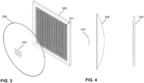
- Figs. 8A to 8C exemplarily illustrate the fourth exemplary implementation in which a quantum information entity 810 is located in the focal point of a hollow parabolic mirror 830.
- Fig. 8A provides an angled view of the fourth exemplary implementation.
- Fig. 8B provides a side view of the fourth exemplary implementation.
- Fig. 8B provides exemplary optical rays 850, 851 for an emission of the quantum emitter 810.
- the reflector 820 may be a SLM.
- the parabolic mirror 830 may be adapted to guide an emission onto the SLM 820.
- a position of the parabolic mirror 830 and/or a position of the quantum emitter 810 are adjusted such that the quantum emitter 810 is located at a focal point within the parabolic mirror 830.
- the adjustment of the position of the mirror may be performed independently of the adjustment of the position of the emitter. The adjustment may be performed using the controller as explained above.
- the SLM may guide an emission of the quantum emitter into the first spatial direction and to reflect an emission into a second spatial direction according to the boundary condition.
- the pixels of the SLM may be controlled to obtain destructive interference for an emission in a second direction.
- the SLM may be controlled to not obtain destructive interference in a first direction.
- the SLM may be controlled to obtain constructive interference in said first direction.
- the flat mirror 821 may include the portion for guiding an emission into the first spatial direction. Moreover, the flat mirror may reflect an emission into a second spatial direction according to the boundary condition. In other words, the flat mirror is located such that destructive interference is obtained for emissions that are directed onto the flat mirror by the parabolic mirror.
- the flat mirror may include a portion 840, such as an opening or the like, in a first spatial direction. In said first spatial direction no destructive interference is obtained.
- the method may include the controlling S1010 of the position of the reflector and/or the emitter.
- the method is not limited to such a controlling.
- the method may provide the functionality as described above for the apparatus.
- any of the steps of the method described above may be included as code instructions in a program, which may be executed by one or more processors.
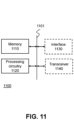
- Fig. 11 shows an exemplary controller 1100, which is included in the apparatus described in the present disclosure.
- the controller may control the positions of a reflector and/or an emitter and may additionally control further components included in the apparatus for suppressing or guiding an emission.
- a device may include memory 1110, processing circuitry 1120, and possibly a transceiver 1140 and a user interface 1130.
- the device may be, for instance a (part of) a computing device or any other suitable device.
- the memory 1110 may store the program, which may be executed by the processing circuitry 1120 to perform steps of any of the above-mentioned methods.
- the processing circuitry may comprise one or more processors and/or other dedicated or programmable hardware.
- the transceiver 1140 may be configured to receive and/or transmit (controlling) signals.
- the device 1100 may further include a user interface 1130 for displaying messages or status of the device, or the like and/or for receiving a user's input.
- a bus 1101 interconnects the memory, the processing circuitry, the transceiver, and the user interface.
- controller may be implemented by any hardware means, apart from using a general purpose processor, it can be implemented as a micro-controller, by means of a programmable hardware such as field programmable gate array (FPGA) or as a specialized hardware such as an application-specific integrated circuit (ASIC). Any combination of the above-mentioned hardware and possibly a software may be used.
- FPGA field programmable gate array
- ASIC application-specific integrated circuit
- the reflector is adapted to reflect emissions of the at least two quantum emitters out of the two or more emitters simultaneously.
- the apparatus further includes a controller configured to control one or more of a position of the reflector and/or a position of an emitter out of the two or more emitters, and a reflection property of the reflector including a phase of the reflected emission based on the boundary condition.
- the reflector includes one or more of a mirror and a spatial light modulator, SLM.
Landscapes
- Physics & Mathematics (AREA)
- Engineering & Computer Science (AREA)
- Chemical & Material Sciences (AREA)
- Nanotechnology (AREA)
- Spectroscopy & Molecular Physics (AREA)
- General Engineering & Computer Science (AREA)
- High Energy & Nuclear Physics (AREA)
- Optics & Photonics (AREA)
- Biophysics (AREA)
- Crystallography & Structural Chemistry (AREA)
- Life Sciences & Earth Sciences (AREA)
- General Physics & Mathematics (AREA)
- Optical Modulation, Optical Deflection, Nonlinear Optics, Optical Demodulation, Optical Logic Elements (AREA)
Claims (10)
- Vorrichtung (200) zum Führen spontaner Emissionen eines Quantenemitters (230) in einer ersten räumlichen Richtung, aufweisendden Quantenemitter (230),dadurch gekennzeichnet, dass der Quantenemitter ein Ion oder ein Atom ist;einen Reflektor (210), der so beschaffen ist, dass er eine Emission des Quantenemitters (230) in einer zweiten räumlichen Richtung gemäß einer Randbedingung reflektiert, wobei die Randbedingung das Erreichen einer destruktiven Interferenz der reflektierten Emission mit der Emission des Quantenemitters (230) umfasst,wobei der Reflektor (210) einen Abschnitt umfasst, der angepasst ist, um eine Emission des Quantenemitters (230) in eine erste räumliche Richtung zu leiten; undeine Steuerung (250), die angepasst ist, um eine oder mehrere der folgenden zu steuern- eine Position des Reflektors (210) und/oder eine Position des Quantenemitters (230) auf Basis der Randbedingung, und- eine Brennweite des Reflektors (210).
- Vorrichtung (200) nach Anspruch 1, wobei die Führung der Emission in der ersten räumlichen Richtung das Nicht-Erhalten einer destruktiven Interferenz mit der Emission des Quantenemitters (230) in der ersten räumlichen Richtung umfasst.
- Vorrichtung (200) gemäß einem der Ansprüche 1 bis 2, wobei der Reflektor (210) einen Spiegel und/oder einen räumlichen Lichtmodulator (SLM) umfasst.
- Vorrichtung (200) gemäß einem der Ansprüche 1 bis 3, wobei der Abschnitt zum Führen einer Emission des Quantenemitters (230) in einer ersten räumlichen Richtung eine Öffnung in der ersten räumlichen Richtung umfasst.
- Vorrichtung (200) gemäß einem der Ansprüche 1 bis 4, wobei der Abschnitt zum Führen einer Emission des Quantenemitters (230) in der ersten räumlichen Richtung eine optische Vorrichtung zum Führen der Emission in der ersten räumlichen Richtung umfasst.
- Vorrichtung (200) gemäß einem der Ansprüche 1 bis 5, wobeider Reflektor ein halbkugelförmiger Spiegel (720) ist undeine Position des halbkugelförmigen Spiegels (720) und/oder eine Position des Quantenemitters (230, 710) so eingestellt sind, dass der Quantenemitter (230, 710) an einem Brennpunkt des halbkugelförmigen Spiegels (720) angeordnet ist.
- Vorrichtung (200) gemäß einem der Ansprüche 1 bis 5, wobeider Reflektor ein SLM (820) ist,die Vorrichtung ferner einen Parabolspiegel (830) umfasst, wobei der Parabolspiegel (830) so angepasst ist, dass er eine Emission auf den SLM (820) lenkt,eine Position des Parabolspiegels (830) und/oder eine Position des Quantenemitters (230, 810) so eingestellt sind, dass der Quantenemitter (230, 810) an einem Brennpunkt innerhalb des Parabolspiegels (830) angeordnet ist, unddas SLM (820) so konfiguriert ist, dass es eine Emission des Quantenemitters (230, 810) in die erste räumliche Richtung leitet und eine Emission des Quantenemitters (230, 810) in eine zweite räumliche Richtung gemäß der Randbedingung reflektiert.
- Vorrichtung (200) gemäß einem der Ansprüche 1 bis 5, wobeider Reflektor ein flacher Spiegel (821) ist,die Vorrichtung ferner einen Parabolspiegel (830) umfasst, wobei der Parabolspiegel (830) so angepasst ist, dass er eine Emission auf den flachen Spiegel (821) lenkt,eine Position des Parabolspiegels (830) und/oder eine Position des Quantenemitters (230, 810) so eingestellt sind, dass der Quantenemitter (230, 810) an einem Brennpunkt innerhalb des Parabolspiegels (830) angeordnet ist,der flache Spiegel (821) den Abschnitt (840) zum Leiten einer Emission des Quantenemitters in die erste räumliche Richtung umfasst,der flache Spiegel (821) angepasst ist, um eine Emission des Quantenemitters (230, 810) in eine zweite räumliche Richtung gemäß der Randbedingung zu reflektieren.
- Vorrichtung (200) gemäß einem der Ansprüche 1 bis 8, wobei die Vorrichtung (200) ferner eine Anordnung von zwei oder mehr Quantenemittern (220) umfasst, wobei die Anordnung den Quantenemitter (230) umfasst.
- Verfahren zum Lenken spontaner Emissionen eines Quantenemitters (230) in eine erste räumliche Richtung, gekennzeichnet durchSteuern (S1010) durch eine Steuerung von einem oder mehreren von- einer Position eines Reflektors (210) und/oder einer Position des Quantenemitters (230) auf Basis der Randbedingung und- einer Brennweite des Reflektors (210);Reflektieren (S1020) einer Emission des Quantenemitters (230) in einer zweiten räumlichen Richtung durch den Reflektor (210) gemäß einer Randbedingung,wobei der Quantenemitter ein Ion oder ein Atom ist und die Randbedingung das Erhalten einer destruktiven Interferenz der reflektierten Emission mit der Emission des Quantenemitters (230) umfasst, undLeiten (S1030) einer Emission des Quantenemitters (230) in der ersten räumlichen Richtung.
Priority Applications (2)
| Application Number | Priority Date | Filing Date | Title |
|---|---|---|---|
| EP23171089.8A EP4458760B1 (de) | 2023-05-02 | 2023-05-02 | Lenkung spontaner emissionen |
| US18/652,196 US20240372033A1 (en) | 2023-05-02 | 2024-05-01 | Guiding of Spontaneous Emissions |
Applications Claiming Priority (1)
| Application Number | Priority Date | Filing Date | Title |
|---|---|---|---|
| EP23171089.8A EP4458760B1 (de) | 2023-05-02 | 2023-05-02 | Lenkung spontaner emissionen |
Publications (3)
| Publication Number | Publication Date |
|---|---|
| EP4458760A1 EP4458760A1 (de) | 2024-11-06 |
| EP4458760C0 EP4458760C0 (de) | 2025-07-02 |
| EP4458760B1 true EP4458760B1 (de) | 2025-07-02 |
Family
ID=86328567
Family Applications (1)
| Application Number | Title | Priority Date | Filing Date |
|---|---|---|---|
| EP23171089.8A Active EP4458760B1 (de) | 2023-05-02 | 2023-05-02 | Lenkung spontaner emissionen |
Country Status (2)
| Country | Link |
|---|---|
| US (1) | US20240372033A1 (de) |
| EP (1) | EP4458760B1 (de) |
Family Cites Families (1)
| Publication number | Priority date | Publication date | Assignee | Title |
|---|---|---|---|---|
| GB2366666B (en) * | 2000-09-11 | 2002-12-04 | Toshiba Res Europ Ltd | An optical device and method for its manufacture |
-
2023
- 2023-05-02 EP EP23171089.8A patent/EP4458760B1/de active Active
-
2024
- 2024-05-01 US US18/652,196 patent/US20240372033A1/en active Pending
Also Published As
| Publication number | Publication date |
|---|---|
| EP4458760C0 (de) | 2025-07-02 |
| US20240372033A1 (en) | 2024-11-07 |
| EP4458760A1 (de) | 2024-11-06 |
Similar Documents
| Publication | Publication Date | Title |
|---|---|---|
| CN113711244B (zh) | 基于多量子位门的量子计算机架构 | |
| EP3815006B1 (de) | Effiziente kühlung von ionenketten für die quantenrechnung | |
| US12159198B2 (en) | Method of computing a solution to a computational problem using a quantum system and apparatus for computing solutions to computational problems | |
| US6988058B1 (en) | Quantum computation with quantum dots and terahertz cavity quantum electrodynamics | |
| Bromberg et al. | Bloch oscillations of path-entangled photons | |
| Shi | Rydberg quantum gates free from blockade error | |
| Zalivako et al. | Quantum computing with trapped ions: principles, achievements, and prospects | |
| EP4458760B1 (de) | Lenkung spontaner emissionen | |
| EP4459370A1 (de) | Unterdrückung spontaner emissionen | |
| Takasu et al. | Quantum degenerate gases of ytterbium atoms | |
| Máximo et al. | Optical binding with cold atoms | |
| US20260058031A1 (en) | Transverse State-Dependent Force for Trapped Ion Entanglement | |
| Wolswijk et al. | Trapping, manipulating and probing ultracold atoms: a quantum technologies tutorial | |
| Takamoto et al. | Coherence of spin-polarized fermions interacting with a clock laser in a Stark-shift-free optical lattice | |
| US20230420241A1 (en) | Single-Sided Standing Wave for Exciting Trapped Ions | |
| US20250364151A1 (en) | Magnetic Optical Trap Device, Physics Package, Physics Package for Optical Lattice Clock, Physics Package for Atomic Clock, Physics Package for Atomic Interferometer, Physics Package for Quantum Information Processing Device, and Physics Package System | |
| Brownnutt | 88Sr Ion Trapping Techniques and Technologies for Quantum Information Processing | |
| JP2003298153A (ja) | 単一光子発生素子 | |
| Sinclair | An introduction to trapped ions, scalability and quantum metrology | |
| Schwegler | Quantum Logic Detection of a Single H2+ Molecule | |
| Schmidt‐Kaler et al. | Quantum computing experiments with cold trapped ions | |
| Poschinger | Quantum optics experiments in a microstructured ion trap | |
| Nguyen | Trapped Ions: From Error Correction to Simulation of Quantum Field Theories | |
| Baker Jr | Precursor Proof‐of‐Concept Experiments for Various Categories of High‐Frequency Gravitational Wave (HFGW) Generators | |
| Simon | Atomic and Ionic Systems |
Legal Events
| Date | Code | Title | Description |
|---|---|---|---|
| PUAI | Public reference made under article 153(3) epc to a published international application that has entered the european phase |
Free format text: ORIGINAL CODE: 0009012 |
|
| STAA | Information on the status of an ep patent application or granted ep patent |
Free format text: STATUS: REQUEST FOR EXAMINATION WAS MADE |
|
| 17P | Request for examination filed |
Effective date: 20240417 |
|
| AK | Designated contracting states |
Kind code of ref document: A1 Designated state(s): AL AT BE BG CH CY CZ DE DK EE ES FI FR GB GR HR HU IE IS IT LI LT LU LV MC ME MK MT NL NO PL PT RO RS SE SI SK SM TR |
|
| GRAP | Despatch of communication of intention to grant a patent |
Free format text: ORIGINAL CODE: EPIDOSNIGR1 |
|
| STAA | Information on the status of an ep patent application or granted ep patent |
Free format text: STATUS: GRANT OF PATENT IS INTENDED |
|
| INTG | Intention to grant announced |
Effective date: 20250116 |
|
| GRAS | Grant fee paid |
Free format text: ORIGINAL CODE: EPIDOSNIGR3 |
|
| GRAA | (expected) grant |
Free format text: ORIGINAL CODE: 0009210 |
|
| STAA | Information on the status of an ep patent application or granted ep patent |
Free format text: STATUS: THE PATENT HAS BEEN GRANTED |
|
| AK | Designated contracting states |
Kind code of ref document: B1 Designated state(s): AL AT BE BG CH CY CZ DE DK EE ES FI FR GB GR HR HU IE IS IT LI LT LU LV MC ME MK MT NL NO PL PT RO RS SE SI SK SM TR |
|
| REG | Reference to a national code |
Ref country code: GB Ref legal event code: FG4D |
|
| REG | Reference to a national code |
Ref country code: CH Ref legal event code: EP |
|
| REG | Reference to a national code |
Ref country code: DE Ref legal event code: R096 Ref document number: 602023004409 Country of ref document: DE |
|
| REG | Reference to a national code |
Ref country code: IE Ref legal event code: FG4D |
|
| U01 | Request for unitary effect filed |
Effective date: 20250702 |
|
| U07 | Unitary effect registered |
Designated state(s): AT BE BG DE DK EE FI FR IT LT LU LV MT NL PT RO SE SI Effective date: 20250709 |
|
| PG25 | Lapsed in a contracting state [announced via postgrant information from national office to epo] |
Ref country code: IS Free format text: LAPSE BECAUSE OF FAILURE TO SUBMIT A TRANSLATION OF THE DESCRIPTION OR TO PAY THE FEE WITHIN THE PRESCRIBED TIME-LIMIT Effective date: 20251102 |
|
| PG25 | Lapsed in a contracting state [announced via postgrant information from national office to epo] |
Ref country code: NO Free format text: LAPSE BECAUSE OF FAILURE TO SUBMIT A TRANSLATION OF THE DESCRIPTION OR TO PAY THE FEE WITHIN THE PRESCRIBED TIME-LIMIT Effective date: 20251002 |
|
| PG25 | Lapsed in a contracting state [announced via postgrant information from national office to epo] |
Ref country code: HR Free format text: LAPSE BECAUSE OF FAILURE TO SUBMIT A TRANSLATION OF THE DESCRIPTION OR TO PAY THE FEE WITHIN THE PRESCRIBED TIME-LIMIT Effective date: 20250702 |
|
| PG25 | Lapsed in a contracting state [announced via postgrant information from national office to epo] |
Ref country code: GR Free format text: LAPSE BECAUSE OF FAILURE TO SUBMIT A TRANSLATION OF THE DESCRIPTION OR TO PAY THE FEE WITHIN THE PRESCRIBED TIME-LIMIT Effective date: 20251003 |
|
| PG25 | Lapsed in a contracting state [announced via postgrant information from national office to epo] |
Ref country code: CZ Free format text: LAPSE BECAUSE OF FAILURE TO SUBMIT A TRANSLATION OF THE DESCRIPTION OR TO PAY THE FEE WITHIN THE PRESCRIBED TIME-LIMIT Effective date: 20250702 |
|
| PG25 | Lapsed in a contracting state [announced via postgrant information from national office to epo] |
Ref country code: PL Free format text: LAPSE BECAUSE OF FAILURE TO SUBMIT A TRANSLATION OF THE DESCRIPTION OR TO PAY THE FEE WITHIN THE PRESCRIBED TIME-LIMIT Effective date: 20250702 |
|
| PG25 | Lapsed in a contracting state [announced via postgrant information from national office to epo] |
Ref country code: RS Free format text: LAPSE BECAUSE OF FAILURE TO SUBMIT A TRANSLATION OF THE DESCRIPTION OR TO PAY THE FEE WITHIN THE PRESCRIBED TIME-LIMIT Effective date: 20251002 |
|
| PG25 | Lapsed in a contracting state [announced via postgrant information from national office to epo] |
Ref country code: ES Free format text: LAPSE BECAUSE OF FAILURE TO SUBMIT A TRANSLATION OF THE DESCRIPTION OR TO PAY THE FEE WITHIN THE PRESCRIBED TIME-LIMIT Effective date: 20250702 |
|
| PG25 | Lapsed in a contracting state [announced via postgrant information from national office to epo] |
Ref country code: SM Free format text: LAPSE BECAUSE OF FAILURE TO SUBMIT A TRANSLATION OF THE DESCRIPTION OR TO PAY THE FEE WITHIN THE PRESCRIBED TIME-LIMIT Effective date: 20250702 |
|
| PG25 | Lapsed in a contracting state [announced via postgrant information from national office to epo] |
Ref country code: SK Free format text: LAPSE BECAUSE OF FAILURE TO SUBMIT A TRANSLATION OF THE DESCRIPTION OR TO PAY THE FEE WITHIN THE PRESCRIBED TIME-LIMIT Effective date: 20250702 |