EP4458759A1 - Microfluidic chip and method for manufacturing microfluidic chip - Google Patents
Microfluidic chip and method for manufacturing microfluidic chip Download PDFInfo
- Publication number
- EP4458759A1 EP4458759A1 EP22915981.9A EP22915981A EP4458759A1 EP 4458759 A1 EP4458759 A1 EP 4458759A1 EP 22915981 A EP22915981 A EP 22915981A EP 4458759 A1 EP4458759 A1 EP 4458759A1
- Authority
- EP
- European Patent Office
- Prior art keywords
- inclined surface
- fluidic channel
- microfluidic chip
- layer
- substrate
- Prior art date
- Legal status (The legal status is an assumption and is not a legal conclusion. Google has not performed a legal analysis and makes no representation as to the accuracy of the status listed.)
- Pending
Links
- 238000000034 method Methods 0.000 title claims abstract description 41
- 238000004519 manufacturing process Methods 0.000 title description 2
- 238000005192 partition Methods 0.000 claims abstract description 388
- 239000000758 substrate Substances 0.000 claims abstract description 191
- 229920005989 resin Polymers 0.000 claims abstract description 183
- 239000011347 resin Substances 0.000 claims abstract description 183
- 239000000463 material Substances 0.000 claims abstract description 43
- 238000011161 development Methods 0.000 claims description 52
- 230000007423 decrease Effects 0.000 claims description 39
- 239000012790 adhesive layer Substances 0.000 claims description 23
- 238000004140 cleaning Methods 0.000 claims description 12
- 239000010410 layer Substances 0.000 description 603
- 230000001965 increasing effect Effects 0.000 description 35
- 239000012530 fluid Substances 0.000 description 28
- 238000011282 treatment Methods 0.000 description 17
- 238000010586 diagram Methods 0.000 description 14
- 238000013459 approach Methods 0.000 description 13
- 229920002120 photoresistant polymer Polymers 0.000 description 13
- 239000000243 solution Substances 0.000 description 13
- 238000006243 chemical reaction Methods 0.000 description 12
- 239000007788 liquid Substances 0.000 description 12
- 230000002708 enhancing effect Effects 0.000 description 11
- 239000000853 adhesive Substances 0.000 description 10
- 230000001070 adhesive effect Effects 0.000 description 10
- 239000010408 film Substances 0.000 description 8
- 230000003247 decreasing effect Effects 0.000 description 7
- 238000012360 testing method Methods 0.000 description 7
- 238000002834 transmittance Methods 0.000 description 7
- 238000012986 modification Methods 0.000 description 6
- 230000004048 modification Effects 0.000 description 6
- 239000011521 glass Substances 0.000 description 5
- 229920005990 polystyrene resin Polymers 0.000 description 5
- 239000004925 Acrylic resin Substances 0.000 description 4
- 229920000178 Acrylic resin Polymers 0.000 description 4
- 239000004743 Polypropylene Substances 0.000 description 4
- 238000005516 engineering process Methods 0.000 description 4
- 238000010438 heat treatment Methods 0.000 description 4
- -1 polypropylene Polymers 0.000 description 4
- 229920001155 polypropylene Polymers 0.000 description 4
- 229920002803 thermoplastic polyurethane Polymers 0.000 description 4
- KFZMGEQAYNKOFK-UHFFFAOYSA-N Isopropanol Chemical compound CC(C)O KFZMGEQAYNKOFK-UHFFFAOYSA-N 0.000 description 3
- KWYUFKZDYYNOTN-UHFFFAOYSA-M Potassium hydroxide Chemical compound [OH-].[K+] KWYUFKZDYYNOTN-UHFFFAOYSA-M 0.000 description 3
- 238000001035 drying Methods 0.000 description 3
- 229920005668 polycarbonate resin Polymers 0.000 description 3
- 239000004431 polycarbonate resin Substances 0.000 description 3
- 229920001225 polyester resin Polymers 0.000 description 3
- 239000004645 polyester resin Substances 0.000 description 3
- 239000000126 substance Substances 0.000 description 3
- 239000010409 thin film Substances 0.000 description 3
- XLYOFNOQVPJJNP-UHFFFAOYSA-N water Substances O XLYOFNOQVPJJNP-UHFFFAOYSA-N 0.000 description 3
- 229920000089 Cyclic olefin copolymer Polymers 0.000 description 2
- CDBYLPFSWZWCQE-UHFFFAOYSA-L Sodium Carbonate Chemical compound [Na+].[Na+].[O-]C([O-])=O CDBYLPFSWZWCQE-UHFFFAOYSA-L 0.000 description 2
- 238000004458 analytical method Methods 0.000 description 2
- 210000004027 cell Anatomy 0.000 description 2
- 229920001577 copolymer Polymers 0.000 description 2
- 150000001925 cycloalkenes Chemical class 0.000 description 2
- 239000004205 dimethyl polysiloxane Substances 0.000 description 2
- 235000013870 dimethyl polysiloxane Nutrition 0.000 description 2
- 238000007599 discharging Methods 0.000 description 2
- 230000000694 effects Effects 0.000 description 2
- 239000003822 epoxy resin Substances 0.000 description 2
- 230000002068 genetic effect Effects 0.000 description 2
- 239000000113 methacrylic resin Substances 0.000 description 2
- 238000000206 photolithography Methods 0.000 description 2
- 238000009832 plasma treatment Methods 0.000 description 2
- 229920000435 poly(dimethylsiloxane) Polymers 0.000 description 2
- 229920003229 poly(methyl methacrylate) Polymers 0.000 description 2
- 229920000647 polyepoxide Polymers 0.000 description 2
- 239000004926 polymethyl methacrylate Substances 0.000 description 2
- 238000012545 processing Methods 0.000 description 2
- 230000000717 retained effect Effects 0.000 description 2
- 229920002050 silicone resin Polymers 0.000 description 2
- 239000002904 solvent Substances 0.000 description 2
- 238000001228 spectrum Methods 0.000 description 2
- 238000004528 spin coating Methods 0.000 description 2
- 239000007921 spray Substances 0.000 description 2
- 229920003002 synthetic resin Polymers 0.000 description 2
- 239000000057 synthetic resin Substances 0.000 description 2
- WGTYBPLFGIVFAS-UHFFFAOYSA-M tetramethylammonium hydroxide Chemical compound [OH-].C[N+](C)(C)C WGTYBPLFGIVFAS-UHFFFAOYSA-M 0.000 description 2
- 241000894006 Bacteria Species 0.000 description 1
- VYZAMTAEIAYCRO-UHFFFAOYSA-N Chromium Chemical compound [Cr] VYZAMTAEIAYCRO-UHFFFAOYSA-N 0.000 description 1
- RYGMFSIKBFXOCR-UHFFFAOYSA-N Copper Chemical compound [Cu] RYGMFSIKBFXOCR-UHFFFAOYSA-N 0.000 description 1
- ISWSIDIOOBJBQZ-UHFFFAOYSA-N Phenol Chemical compound OC1=CC=CC=C1 ISWSIDIOOBJBQZ-UHFFFAOYSA-N 0.000 description 1
- 239000004721 Polyphenylene oxide Substances 0.000 description 1
- 239000004793 Polystyrene Substances 0.000 description 1
- XUIMIQQOPSSXEZ-UHFFFAOYSA-N Silicon Chemical compound [Si] XUIMIQQOPSSXEZ-UHFFFAOYSA-N 0.000 description 1
- WGLPBDUCMAPZCE-UHFFFAOYSA-N Trioxochromium Chemical compound O=[Cr](=O)=O WGLPBDUCMAPZCE-UHFFFAOYSA-N 0.000 description 1
- 239000002253 acid Substances 0.000 description 1
- 230000001154 acute effect Effects 0.000 description 1
- 239000007864 aqueous solution Substances 0.000 description 1
- 230000015572 biosynthetic process Effects 0.000 description 1
- 238000009835 boiling Methods 0.000 description 1
- 238000009395 breeding Methods 0.000 description 1
- 230000001488 breeding effect Effects 0.000 description 1
- QHIWVLPBUQWDMQ-UHFFFAOYSA-N butyl prop-2-enoate;methyl 2-methylprop-2-enoate;prop-2-enoic acid Chemical compound OC(=O)C=C.COC(=O)C(C)=C.CCCCOC(=O)C=C QHIWVLPBUQWDMQ-UHFFFAOYSA-N 0.000 description 1
- 238000006555 catalytic reaction Methods 0.000 description 1
- 229910052804 chromium Inorganic materials 0.000 description 1
- 239000011651 chromium Substances 0.000 description 1
- 229910000423 chromium oxide Inorganic materials 0.000 description 1
- 210000000349 chromosome Anatomy 0.000 description 1
- 239000011248 coating agent Substances 0.000 description 1
- 238000000576 coating method Methods 0.000 description 1
- 238000011109 contamination Methods 0.000 description 1
- 238000007796 conventional method Methods 0.000 description 1
- 229910052802 copper Inorganic materials 0.000 description 1
- 239000010949 copper Substances 0.000 description 1
- 238000003851 corona treatment Methods 0.000 description 1
- 238000005520 cutting process Methods 0.000 description 1
- 238000001514 detection method Methods 0.000 description 1
- 239000003814 drug Substances 0.000 description 1
- 229940079593 drug Drugs 0.000 description 1
- 238000009509 drug development Methods 0.000 description 1
- 239000000428 dust Substances 0.000 description 1
- 230000007613 environmental effect Effects 0.000 description 1
- 210000003743 erythrocyte Anatomy 0.000 description 1
- 238000005530 etching Methods 0.000 description 1
- UHESRSKEBRADOO-UHFFFAOYSA-N ethyl carbamate;prop-2-enoic acid Chemical compound OC(=O)C=C.CCOC(N)=O UHESRSKEBRADOO-UHFFFAOYSA-N 0.000 description 1
- 238000005187 foaming Methods 0.000 description 1
- 239000000499 gel Substances 0.000 description 1
- LNEPOXFFQSENCJ-UHFFFAOYSA-N haloperidol Chemical compound C1CC(O)(C=2C=CC(Cl)=CC=2)CCN1CCCC(=O)C1=CC=C(F)C=C1 LNEPOXFFQSENCJ-UHFFFAOYSA-N 0.000 description 1
- FFUAGWLWBBFQJT-UHFFFAOYSA-N hexamethyldisilazane Chemical compound C[Si](C)(C)N[Si](C)(C)C FFUAGWLWBBFQJT-UHFFFAOYSA-N 0.000 description 1
- 230000005661 hydrophobic surface Effects 0.000 description 1
- 238000007654 immersion Methods 0.000 description 1
- 239000003999 initiator Substances 0.000 description 1
- 238000002347 injection Methods 0.000 description 1
- 239000007924 injection Substances 0.000 description 1
- 238000001746 injection moulding Methods 0.000 description 1
- 238000011835 investigation Methods 0.000 description 1
- 238000013532 laser treatment Methods 0.000 description 1
- 210000000265 leukocyte Anatomy 0.000 description 1
- 238000001459 lithography Methods 0.000 description 1
- 239000000178 monomer Substances 0.000 description 1
- 238000000465 moulding Methods 0.000 description 1
- JFNLZVQOOSMTJK-KNVOCYPGSA-N norbornene Chemical compound C1[C@@H]2CC[C@H]1C=C2 JFNLZVQOOSMTJK-KNVOCYPGSA-N 0.000 description 1
- 229920003986 novolac Polymers 0.000 description 1
- CXQXSVUQTKDNFP-UHFFFAOYSA-N octamethyltrisiloxane Chemical compound C[Si](C)(C)O[Si](C)(C)O[Si](C)(C)C CXQXSVUQTKDNFP-UHFFFAOYSA-N 0.000 description 1
- 230000003287 optical effect Effects 0.000 description 1
- 238000011369 optimal treatment Methods 0.000 description 1
- 239000003960 organic solvent Substances 0.000 description 1
- 238000004987 plasma desorption mass spectroscopy Methods 0.000 description 1
- 229920006122 polyamide resin Polymers 0.000 description 1
- 239000004417 polycarbonate Substances 0.000 description 1
- 229920000515 polycarbonate Polymers 0.000 description 1
- 229920000570 polyether Polymers 0.000 description 1
- 229920001721 polyimide Polymers 0.000 description 1
- 239000009719 polyimide resin Substances 0.000 description 1
- 229920000642 polymer Polymers 0.000 description 1
- 229920005672 polyolefin resin Polymers 0.000 description 1
- 229920005749 polyurethane resin Polymers 0.000 description 1
- 230000035484 reaction time Effects 0.000 description 1
- 230000009257 reactivity Effects 0.000 description 1
- 238000011160 research Methods 0.000 description 1
- 239000011342 resin composition Substances 0.000 description 1
- 229910052710 silicon Inorganic materials 0.000 description 1
- 239000010703 silicon Substances 0.000 description 1
- 229920002379 silicone rubber Polymers 0.000 description 1
- 239000004945 silicone rubber Substances 0.000 description 1
- 229910000029 sodium carbonate Inorganic materials 0.000 description 1
- 238000005507 spraying Methods 0.000 description 1
- 238000004381 surface treatment Methods 0.000 description 1
- 238000000411 transmission spectrum Methods 0.000 description 1
- 235000012431 wafers Nutrition 0.000 description 1
Images





Classifications
-
- B—PERFORMING OPERATIONS; TRANSPORTING
- B01—PHYSICAL OR CHEMICAL PROCESSES OR APPARATUS IN GENERAL
- B01L—CHEMICAL OR PHYSICAL LABORATORY APPARATUS FOR GENERAL USE
- B01L3/00—Containers or dishes for laboratory use, e.g. laboratory glassware; Droppers
- B01L3/50—Containers for the purpose of retaining a material to be analysed, e.g. test tubes
- B01L3/502—Containers for the purpose of retaining a material to be analysed, e.g. test tubes with fluid transport, e.g. in multi-compartment structures
- B01L3/5027—Containers for the purpose of retaining a material to be analysed, e.g. test tubes with fluid transport, e.g. in multi-compartment structures by integrated microfluidic structures, i.e. dimensions of channels and chambers are such that surface tension forces are important, e.g. lab-on-a-chip
- B01L3/502707—Containers for the purpose of retaining a material to be analysed, e.g. test tubes with fluid transport, e.g. in multi-compartment structures by integrated microfluidic structures, i.e. dimensions of channels and chambers are such that surface tension forces are important, e.g. lab-on-a-chip characterised by the manufacture of the container or its components
-
- B—PERFORMING OPERATIONS; TRANSPORTING
- B01—PHYSICAL OR CHEMICAL PROCESSES OR APPARATUS IN GENERAL
- B01L—CHEMICAL OR PHYSICAL LABORATORY APPARATUS FOR GENERAL USE
- B01L3/00—Containers or dishes for laboratory use, e.g. laboratory glassware; Droppers
- B01L3/50—Containers for the purpose of retaining a material to be analysed, e.g. test tubes
- B01L3/502—Containers for the purpose of retaining a material to be analysed, e.g. test tubes with fluid transport, e.g. in multi-compartment structures
- B01L3/5027—Containers for the purpose of retaining a material to be analysed, e.g. test tubes with fluid transport, e.g. in multi-compartment structures by integrated microfluidic structures, i.e. dimensions of channels and chambers are such that surface tension forces are important, e.g. lab-on-a-chip
- B01L3/502723—Containers for the purpose of retaining a material to be analysed, e.g. test tubes with fluid transport, e.g. in multi-compartment structures by integrated microfluidic structures, i.e. dimensions of channels and chambers are such that surface tension forces are important, e.g. lab-on-a-chip characterised by venting arrangements
-
- G—PHYSICS
- G01—MEASURING; TESTING
- G01N—INVESTIGATING OR ANALYSING MATERIALS BY DETERMINING THEIR CHEMICAL OR PHYSICAL PROPERTIES
- G01N35/00—Automatic analysis not limited to methods or materials provided for in any single one of groups G01N1/00 - G01N33/00; Handling materials therefor
- G01N35/08—Automatic analysis not limited to methods or materials provided for in any single one of groups G01N1/00 - G01N33/00; Handling materials therefor using a stream of discrete samples flowing along a tube system, e.g. flow injection analysis
-
- B—PERFORMING OPERATIONS; TRANSPORTING
- B01—PHYSICAL OR CHEMICAL PROCESSES OR APPARATUS IN GENERAL
- B01L—CHEMICAL OR PHYSICAL LABORATORY APPARATUS FOR GENERAL USE
- B01L2200/00—Solutions for specific problems relating to chemical or physical laboratory apparatus
- B01L2200/06—Fluid handling related problems
- B01L2200/0684—Venting, avoiding backpressure, avoid gas bubbles
-
- B—PERFORMING OPERATIONS; TRANSPORTING
- B01—PHYSICAL OR CHEMICAL PROCESSES OR APPARATUS IN GENERAL
- B01L—CHEMICAL OR PHYSICAL LABORATORY APPARATUS FOR GENERAL USE
- B01L2200/00—Solutions for specific problems relating to chemical or physical laboratory apparatus
- B01L2200/12—Specific details about manufacturing devices
-
- B—PERFORMING OPERATIONS; TRANSPORTING
- B01—PHYSICAL OR CHEMICAL PROCESSES OR APPARATUS IN GENERAL
- B01L—CHEMICAL OR PHYSICAL LABORATORY APPARATUS FOR GENERAL USE
- B01L2300/00—Additional constructional details
- B01L2300/08—Geometry, shape and general structure
- B01L2300/0809—Geometry, shape and general structure rectangular shaped
- B01L2300/0816—Cards, e.g. flat sample carriers usually with flow in two horizontal directions
-
- B—PERFORMING OPERATIONS; TRANSPORTING
- B01—PHYSICAL OR CHEMICAL PROCESSES OR APPARATUS IN GENERAL
- B01L—CHEMICAL OR PHYSICAL LABORATORY APPARATUS FOR GENERAL USE
- B01L2300/00—Additional constructional details
- B01L2300/08—Geometry, shape and general structure
- B01L2300/0887—Laminated structure
-
- B—PERFORMING OPERATIONS; TRANSPORTING
- B01—PHYSICAL OR CHEMICAL PROCESSES OR APPARATUS IN GENERAL
- B01L—CHEMICAL OR PHYSICAL LABORATORY APPARATUS FOR GENERAL USE
- B01L2400/00—Moving or stopping fluids
- B01L2400/08—Regulating or influencing the flow resistance
- B01L2400/084—Passive control of flow resistance
- B01L2400/086—Passive control of flow resistance using baffles or other fixed flow obstructions
Definitions
- the present disclosure relates to microfluidic chips and methods of producing the same.
- micro reaction fields are formed by applying lithography processing or thick film processing technologies to enable testing in units of several microliters to several nanoliters.
- technologies using such a micro reaction field are called ⁇ -TAS (micro total analysis systems).
- ⁇ -TAS is applied to fields such as genetic testing, chromosome testing, cell testing and drug development, biotechnologies, testing of trace substances in the environment, investigation of breeding environments for agricultural products, genetic testing of agricultural products, and the like.
- the introduction of ⁇ -TAS technologies brings significant effects such as automation, higher speed, higher accuracy, lower cost, speed, reduced environmental impact, and the like.
- micrometer-sized fluidic channels formed on a substrate are often used, and such a substrate is called a chip, microchip, microfluidic chip, or the like.
- microfluidic chips have been produced using techniques such as injection molding, molding, cutting, etching, and the like.
- substrates of microfluidic chips glass substrates are typically used since they are easy to produce and suitable for optical detection.
- resin materials which are lightweight, less likely to break than glass substrates, and inexpensive, are being developed.
- a resin pattern for a fluidic channel is formed typically by photolithography, and a lid material is bonded thereto to form a microfluidic chip. According to this method, microfluidic channel patterns, which have been sometimes difficult to produce with conventional techniques, can be formed.
- the present disclosure has been made to provide a microfluidic chip that can enhance adhesion between the wall and the lid material, and a method of producing the microfluidic chip.
- a microfluidic chip includes: a substrate; a partition member made of a resin material, the partition member being disposed on the substrate and defining a fluidic channel; and a cover member disposed on a side of the partition member opposite to that facing the substrate, the cover member covering the fluidic channel, wherein the partition member has a width which increases toward the cover member in cross-sectional view.
- a method of producing a microfluidic chip includes the steps of: applying a resin to a substrate; exposing the applied resin to light; subjecting the exposed resin to development and cleaning to thereby form a partition member that defines a fluidic channel on the substrate; post-baking the partition member; and bonding a cover member to a side of the partition member opposite to that facing the substrate, wherein in the step of exposing the resin, the photosensitive resin is exposed to light having a wavelength of 250 nm or greater and 350 nm or less in the ultraviolet light region, and excess resin on the substrate is removed by the development, whereby the partition member is formed to have a width which increases toward the cover member in cross-sectional view.
- a microfluidic chip that can enhance adhesion between the wall and the lid material can be provided.
- a substrate side of the microfluidic chip may be referred to as "lower side", and a side (lid material side) of the microfluidic chip opposite to that facing the substrate may be referred to as "upper side”.
- the inventors of the present invention have diligently studied and found that, in microfluidic chips, the area of the bonding region for bonding a wall and a lid material to each other can be increased by forming the wall into a specific shape. Accordingly, the inventors have invented a microfluidic chip which can enhance adhesion strength between the wall and the lid material, and a method of producing the microfluidic chip.
- Fig. 1 is a schematic diagram illustrating an example configuration of a microfluidic chip 1 according to a first embodiment of the present disclosure (hereinafter, also referred to as "the present embodiment"). Specifically, Fig. 1(a) is a schematic plan view of the microfluidic chip 1 of the present embodiment. Fig. 1(b) is a schematic cross-sectional diagram illustrating a cross-section of the microfluidic chip 1 taken along the line A-A in Fig. 1(a) .
- the microfluidic chip 1 includes an inlet 4 for introducing a fluid (for example, liquid), a fluidic channel portion 13 through which the fluid introduced through the inlet 4 flows, and an outlet 5 for discharging the fluid from the fluidic channel portion 13.
- a fluid for example, liquid
- the fluidic channel portion 13 is covered with a cover layer 12, and the inlet 4 and the outlet 5 are through holes formed in the cover layer 12. Details of the cover layer 12 will be described later.
- Fig. 1(a) shows the fluidic channel portion 13 as seen through the transparent cover layer 12.
- At least one inlet 4 and at least one outlet 5 may be provided, and a plurality of each may be provided. Further, in the microfluidic chip 1, a plurality of fluidic channel portions 13 may be provided, and the fluidic channel portions 13 may be designed to merge or branch the fluid introduced from the inlet 4.
- the microfluidic chip 1 includes a substrate 10, a partition layer (an example of partition member) 11 provided on the substrate 10 and defining the fluidic channel, and a cover layer (an example of cover member) 12 provided on a side of the partition layer 11 opposite to that facing the substrate 10 and covering the fluidic channel portion 13.
- the fluidic channel portion 13 through which the fluid introduced from the inlet 4 flows is a region surrounded by the substrate 10, the partition layer 11 and the cover layer 12.
- the fluidic channel portion 13 is defined by a pair of partition layers 11 facing each other provided on the substrate 10, and a side of the fluidic channel portion 13 opposite to that facing the substrate 10 is covered with the cover layer 12 as a lid material. As described above, a fluid is introduced into the fluidic channel portion 13 from the inlet 4 (see Fig. 1(a) ) formed in the cover layer 12, and the fluid that has flowed through the fluidic channel portion 13 is discharged from the outlet 5.
- the partition layer 11 in the present embodiment has a width W1 that increases toward the cover layer 12 in cross-sectional view. That is, the width W1 of the partition layer 11 in cross-sectional view increases toward the cover layer 12.
- the substrate 10 is a member that serves as a base of the microfluidic chip 1, and the partition layer 11 provided on the substrate 10 defines the fluidic channel portion 13. That is, the substrate 10 and the partition layer 11 can be regarded as a main body of the microfluidic chip 1.
- the substrate 10 can be made of either a translucent material or a non-translucent material.
- a material having excellent transparency to the light can be used.
- resin, glass, or the like can be used.
- the resin used for the translucent material constituting the substrate 10 include acrylic resin, methacrylic resin, polypropylene, polycarbonate resin, cycloolefin resin, polystyrene resin, polyester resin, urethane resin, silicone resin and fluororesin from the viewpoint of being suitable for forming the main body of the microfluidic chip 1.
- a non-translucent material when the state inside the fluidic channel portion 13 (state of fluid) is not necessarily detected and observed using light, a non-translucent material may be used.
- the non-translucent material include silicon wafers and copper plates.
- the thickness of the substrate 10 is not particularly limited, it is preferably in the range of 10 ⁇ m (0.01 mm) or greater and 10 mm or less since a certain degree of rigidity is required in formation of a fluidic channel.
- the partition layer 11 is disposed on the substrate and forms a fluidic channel portion 13.
- the partition layer 11 can be made of a resin material. Examples of the resin material of the partition layer 11 include a photosensitive resin.
- the photosensitive resin constituting the partition layer 11 is preferably photosensitive to light having a wavelength of 190 nm or greater and 400 nm or less, which is in the ultraviolet light region.
- a photoresist such as liquid resist or dry film resist can be used.
- the photosensitive resin may be either positive type in which the photosensitive region dissolves or negative type in which the photosensitive region becomes insoluble.
- Examples of the photosensitive resin composition suitable for forming the partition layer 11 in the microfluidic chip 1 include radical negative type photosensitive resins containing alkali-soluble polymers, addition polymerizable monomers and photopolymerization initiators.
- the photosensitive resin material examples include acrylic resins, acrylic urethane resins (urethane acrylate resins), epoxy resins, polyamide resins, polyimide resins, polyurethane resins, polyester resins, polyether resins, polyolefin resins, polycarbonate resins, polystyrene resins, norbornene resins, phenol novolac resins, and other photosensitive resins, and these can be used singly, or in combinations or as copolymers of two or more.
- the resin material of the partition layer 11 is not limited to a photosensitive resin, and may be, for example, silicone rubber (PDMS: polydimethylsiloxane) or synthetic resin.
- the synthetic resin include polymethyl methacrylate resin (PMMA), polycarbonate (PC), polystyrene resin (PS), polypropylene (PP), cycloolefin polymer (COP) and cycloolefin copolymer (COC).
- the resin material of the partition layer 11 is preferably selected as appropriate according to the application.
- the thickness of the partition layer 11 on the substrate 10, that is, the height of the fluidic channel portion 13, is not particularly limited, but is required to be greater than the substances to be analyzed or inspected (for example, drugs, bacteria, cells, red blood cells, leukocytes, etc.) contained in the fluid introduced into the fluidic channel portion 13. Therefore, the thickness of the partition layer 11, that is, the height of the fluidic channel portion 13, is preferably in the range of 5 ⁇ m or greater and 100 ⁇ m or less.
- the width of the fluidic channel portion 13 is required to be greater than the substances to be analyzed or inspected, the width of the fluidic channel portion 13 defined by the partition layer 11 is preferably in the range of 5 ⁇ m or greater and 100 ⁇ m or less.
- the length of the fluidic channel defined by the partition layer 11 is preferably in the range of 10 mm or greater and 100 mm or less, more preferably in the range of 30 mm or greater and 70 mm or less, and still more preferably in the range of 40 mm or greater and 60 mm or less.
- the cover layer 12 is a lid material covering the fluidic channel portion 13 as shown in Fig. 1(b) .
- the cover layer 12 is provided on a side of the partition layer 11 opposite to that facing the substrate 10, and the cover layer 12 faces the substrate 10 with the partition layer 11 therebetween. More specifically, as shown in Fig. 1(b) , the cover layer 12 in cross-sectional view has side portions supported by the partition layer 11 and a center region that faces the substrate 10, the center region defining the upper side of the fluidic channel portion 13.
- the cover layer 12 can be made of either a translucent material or a non-translucent material
- a material having excellent transparency to the light can be used.
- resin, glass, or the like can be used.
- the resin constituting the cover layer 12 include acrylic resin, methacrylic resin, polypropylene, polycarbonate resin, cycloolefin resin, polystyrene resin, polyester resin, urethane resin, silicone resin and fluororesin from the viewpoint of being suitable for forming the main body of the microfluidic chip 1.
- the thickness of the cover layer 12 is not particularly limited, but in view of forming through holes corresponding to the inlet 4 and the outlet 5 in the cover layer 12, it is preferably in the range of 10 ⁇ m or greater and 10 mm or less. Further, it is also preferred that holes corresponding to the inlet 4 for introducing a fluid (liquid) and the outlet 5 for discharging a fluid are formed in advance in the cover layer 12 before the cover layer 12 is bonded to the partition layer 11.
- the width W1 of the partition layer 11 of the microfluidic chip 1 increases toward the cover layer 12 in cross-sectional view.
- the "cross-section” in the “cross-sectional view” refers to a cross-section of the microfluidic chip 1 cut in the thickness direction (direction perpendicular to the longitudinal direction of the fluidic channel portion 13), for example, and the cross-section includes at least the partition layer 11, the cover layer 12 and the fluidic channel portion 13.
- the width W1 of the partition layer 11 increases toward the cover layer 12, whereby the area of the bonding region for bonding the partition layer 11 and the cover layer 12 can be increased, enhancing adhesion between the partition layer 11 and the cover layer 12. This can prevent occurrence of liquid leakage, damage, and the like during use of the microfluidic chip 1.
- the shape of the partition layer 11 will be more specifically described.
- the partition layer 11 of the microfluidic chip 1 includes a side surface 110 that defines the fluidic channel portion 13.
- the side surface 110 is connected to the cover layer 12 at an upper end 110a which is an end on the cover layer 12 side. Further, the side surface 110 is connected to the substrate 10 at a lower end 110b which is an end on the substrate 10 side. As shown in Fig. 1(b) , the side surface 110 has an inclined surface 111 that is inclined relative to the cover layer 12.
- the inclined surface 111 will be specifically described below. As shown in Fig. 1(b) , the inclined surface 111 has a planar shape. Further, in the partition layer 11 of the microfluidic chip 1 according to the present embodiment, the inclined surface 111 is provided on the entire side surface 110. More specifically, the inclined surface 111 extends from the upper end 110a to the lower end 110b of the side surface 110, and is connected to the cover layer 12 at the upper end 110a of the side surface 110 and to the substrate 10 at the lower end 110b. That is, the upper end 110a is the upper end of the side surface 110 and the inclined surface 111, and the lower end 110b is the lower end of the side surface 110 and the inclined surface 111.
- the upper end 110a of the side surface 110 (upper end of the inclined surface 111) is located closer to the center of the fluidic channel portion 13 than the lower end 110b is. That is, the upper end 110a of the side surface 110 (upper end of the inclined surface 111) is located closer to the opposing partition layer 11 than the lower end 110b is.
- the lower end 110b of the side surface 110 (lower end of the inclined surface 111) is located further away from the center of the fluidic channel portion 13 than the upper end 110a is. That is, the lower end 110b of the side surface 110 (lower end of the inclined surface 111) is located further away from the opposing partition layer 11 than the upper end 110a is.
- the inclined surface 111 extends upward in an inclined manner from the lower end 110b connected to the cover layer 12 to the upper end 110a, where it is connected to the cover layer 12.
- the width W1 of the partition layer 11 in cross-sectional view increases in the direction toward the center of the fluidic channel portion 13, that is, toward the opposing partition layer 11 in the transverse direction of the fluidic channel portion 13, as it approaches the cover layer 12. Therefore, the width W1 of the partition layer 11 in cross-sectional view increases from the substrate 10 side toward the cover layer 12 side.
- the inclined surface 111 has a planar shape and is provided on the entire side surface 110 of the partition layer 11.
- the width W1 of the partition layer 11 continuously increases toward the cover layer 12.
- the width W1 of the partition layer 11 continuously expands and increases toward the center of the fluidic channel portion 13 (in the transverse direction), as it approaches the cover layer 12.
- the “continuously increases (expands)" herein means that the width W1 of the partition layer 11 continuously increases (expands), without decreasing (reducing), from the lower end 110ba where the inclined surface 111 is connected to the substrate 10 to the upper end 110a where the inclined surface 111 is connected to the cover layer 12 substrate 10.
- the fluidic channel portion 13 has a fluidic channel width W2 defined as the width between a pair of partition layers 11 facing each other, that is, the width between the side surfaces 110.
- the inclined surface 111 is provided on the entire side surface 110, so the fluidic channel width W2 can also be defined as the width between the inclined surfaces 111.
- the width W1 of the partition layer 11 in cross-sectional view increases toward the cover layer 12.
- the width between the inclined surfaces 111 of the pair of partition layers 11 is narrower on the cover layer 12 side than on the substrate 10 side. Therefore, the fluidic channel width W2 of the fluidic channel portion 13 decreases from the substrate 10 side toward the cover layer 12 side.
- the fluidic channel width W2 is widest at the lowest part (bottom) of the fluidic channel portion 13 where a front surface 10a of the substrate 10 is exposed, that is, between the lower ends 110b of the pair of partition layers 11. Further, the fluidic channel width W2 is narrowest at the top of the fluidic channel portion 13 where the cover layer 12 (specifically, a rear surface 12a of the cover layer 12) is exposed, that is, between the upper ends 110a of the pair of partition layers 11.
- the width W1 of the partition layer 11 continuously increases toward the cover layer 12. That is, the width W1 increases in the transverse direction of the fluidic channel portion 13 as it approaches the cover layer 12 such that each of the pair of opposing partition layers 11 approaches the other.
- the width between the inclined surfaces 111 of the pair of partition layers 11 becomes continuously narrower (decreases) toward the cover layer 12. Accordingly, the fluidic channel width W2 of the fluidic channel portion 13 becomes continuously narrower (decreases) toward the cover layer 12. More specifically, the fluidic channel width W2 continuously decreases from the lowest part (bottom) of the fluidic channel portion 13 where the substrate 10 is exposed toward the top of the fluidic channel portion 13 where the cover layer 12 (specifically, the rear surface 12a) is exposed.
- the “continuously decreases” herein means that the fluidic channel width W2 of the fluidic channel portion 13 continuously decreases, without increasing, from the bottom of the fluidic channel portion 13 toward the top of the fluidic channel portion 13.
- the fluidic channel portion 13 has a trapezoidal shape in cross-sectional view.
- the "cross-section” in the “cross-sectional view” refers to a cross-section of the microfluidic chip 1 cut in the thickness direction (direction perpendicular to the longitudinal direction of the fluidic channel portion 13), and the cross-section includes the substrate 10, the partition layer 11, the cover layer 12 and the fluidic channel portion 13.
- the fluidic channel width W2 of the fluidic channel portion 13 continuously decreases toward the cover layer 12.
- the fluidic channel portion 13 includes a bubble trapping region 130 that traps air bubbles in the fluidic channel portion 13.
- the bubble trapping region 130 is formed by the inclined surface 111 of the partition layer 11 and the front surface 10a, which is the surface of the substrate 10 on the fluidic channel portion 13 side.
- Air bubbles may be present in the fluidic channel portion 13, for example, due to entrainment of air bubbles during injection of a fluid such as a reaction solution into the microfluidic chip 1, boiling due to heating of the reaction solution, air entrainment due to nonuniform flow in the microfluidic channel, foaming from the reaction solution itself, or the like.
- the fluidic channel width W2 of the fluidic channel portion 13 decreases toward the cover layer 12. Therefore, if the above air bubbles drift in the fluidic channel portion 13, especially in a center region E1 of the fluidic channel portion 13, which is the region near the center, fluid flow may become unstable, or visibility of the liquid may be reduced when the interior of the fluidic channel portion 13 is observed through the cover layer 12 or the substrate 10.
- the bubble trapping region 130 is a recess formed by the inclined surface 111 (side surface 110) of the partition layer 11 and the front surface 10a of the substrate 10, and the lower end 110b of the inclined surface 111 is the deepest portion. More specifically, the bubble trapping region 130 is a corner formed by the inclined surface 111 of the partition layer 11 and the front surface 10a of the substrate 10 connected to each other at the lower end 110b of the inclined surface 111. That is, the bubble trapping region 130 is formed on each of the left and right sides of the lowest part (bottom) of the fluidic channel at which the fluidic channel width W2 of the fluidic channel portion 13 is widest.
- the microfluidic chip 1 can further stabilize fluid flow and further improve the visibility during observation of the interior of the fluidic channel portion 13.
- Air bubbles in the fluidic channel portion 13 migrate in the fluid (e.g., reaction solution) from the center region E1 toward the left and right sides of the fluidic channel portion 13 due to pressure or the like when the fluid flows, and are collected in the bubble trapping regions 130.
- the interior angle of the bubble trapping region 130 which is formed as a corner is an acute angle (less than 90 degrees). Accordingly, air bubbles collected in the bubble trapping region 130 are likely to remain in the bubble trapping region 130, and are less likely to leave (return) toward the center region E1 of the channel portion 13.
- the microfluidic chip 1 includes the substrate 10, the partition layer 11 made of a resin material, the partition layer 11 being disposed on the substrate 10 and defining the fluidic channel portion 13, and the cover layer 12 disposed on a side of the partition layer 11 opposite to that facing the substrate 10, the cover layer 12 covering the fluidic channel portion 13, wherein the partition layer 11 has a width which increases toward the cover layer 12 in cross-sectional view.
- the microfluidic chip 1 can enhance adhesion between the wall (partition layer 11) and the lid material (cover layer 12).
- the fluidic channel portion 13 includes the bubble trapping region 130 that traps air bubbles in the fluidic channel portion 13, and the bubble trapping region 130 is formed by the inclined surface 111 of the partition layer 11 and a surface (front surface 10a) of the substrate 10 on the fluidic channel portion 13 side.
- the microfluidic chip 1 can stabilize fluid flow and improves visibility during observation of the interior of the fluidic channel portion 13.
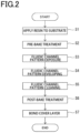
- FIG. 2 is a flowchart showing an example method of producing a microfluidic chip 1 according to the present embodiment.
- the partition layer 11 is made of a photosensitive resin.
- a step of applying a resin to the substrate 10 is first performed.
- a resin layer for forming the partition layer 11 is provided on the substrate 10.
- a resin layer (photosensitive resin layer) made of a photosensitive resin, for example, may be formed on the substrate 10.
- the photosensitive resin layer may be formed on the substrate 10 by, for example, applying a photosensitive resin to the substrate 10.
- the application may be performed by, for example, spin coating, spray coating, bar coating, or the like, and in particular, spin coating is preferred from the perspective of controlling the film thickness.
- Various forms of photosensitive resin such as liquid, gel and film, can be applied to the substrate 10. In particular, it is preferred to form a photosensitive resin layer using a liquid resist.
- the resin for example, photosensitive resin
- the resin layer for example, photosensitive resin layer
- the thickness of the resin layer that is, thickness of the partition layer 11 becomes in the range of 5 ⁇ m or greater and 100 ⁇ m or less.
- a step of heat treatment is performed to remove the solvent contained in the resin (for example, photosensitive resin) applied to the substrate 10.
- the pre-bake treatment is not an essential step, and may be appropriately performed at an optimal temperature and time according to the characteristics of the resin.
- the pre-bake temperature and time are appropriately set to optimal conditions according to the characteristics of the photosensitive resin.
- a step of exposing the resin (for example, photosensitive resin) applied to the substrate 10 is performed. Specifically, exposure is performed to draw a fluidic channel pattern on the photosensitive resin applied to the substrate 10. Exposure may be performed with, for example, an exposure device using ultraviolet light as a light source or a laser drawing device. In particular, exposure with a proximity exposure device or a contact exposure device using ultraviolet light as a light source is preferred. When using a proximity exposure device, exposure is performed via a photomask having a fluidic channel pattern of the microfluidic chip 1.
- the photomask may be one having a light-shielding film with a bilayer structure of chromium and chromium oxide.
- the partition layer 11 is formed of a photosensitive resin that is photosensitive to light having a wavelength of 190 nm or greater and 400 nm or less, which is in the ultraviolet light region. Accordingly, in this step (exposure step), the photosensitive resin applied to the substrate 10 may be exposed to light having a wavelength of 190 nm or greater and 400 nm or less.
- heat treatment post exposure bake: PEB
- PEB post exposure bake
- a step of subjecting the exposed photosensitive resin to development is performed to form a fluidic channel pattern.
- Development may be performed by reaction between the photosensitive resin and a developer using, for example, a spray, dip or puddle type development device.
- the developer include a sodium carbonate aqueous solution, tetramethylammonium hydroxide, potassium hydroxide and organic solvents.
- the developer is not limited to those described above, and a developer most suitable for the characteristics of the photosensitive resin may be appropriately used. Further, the concentration and development treatment time may be appropriately adjusted to optimal conditions according to the characteristics of the photosensitive resin.
- a step of cleaning is performed to completely remove the developer used for development from the resin layer (photosensitive resin layer) on the substrate 10.
- Cleaning may be performed using, for example, a spray, shower or immersion type cleaning device.
- the cleaning solution include pure water, isopropyl alcohol, and the like, and the cleaning solution most suitable for removing the developer used for the development treatment may be appropriately used.
- drying is performed using a spin dryer, IPA vapor dryer, or by natural drying, or the like.
- a step of heat treatment (post-bake) is performed on the partition layer 11 constituting the fluidic channel pattern, that is, the fluidic channel portion 13.
- This post-bake treatment removes residual water from development and cleaning.
- the post-bake treatment may be performed using, for example, a hot plate, oven, or the like.
- the developer and water from cleaning may remain in the partition layer 11.
- the solvent that has not been removed in the pre-bake treatment may also remain in the partition layer 11. These can be removed by the post-bake treatment.
- a step of bonding is performed to bond the cover layer 12 to the partition layer 11 after the post-bake treatment.
- the cover layer 12 is bonded to a side of the partition layer 11 opposite to that facing the substrate 10.
- the fluidic channel portion 13 is covered with the cover layer 12, and the microfluidic chip 1 shown in Fig. 1(a) and Fig. 1(b) is formed.
- the method of bonding the partition layer 11 and the cover layer 12 may be a method by thermocompression bonding after applying a surface modification treatment to the bonding surfaces of the partition layer 11 and the cover layer 12, a method using an adhesive, or a method of bonding by applying a surface modification treatment to the bonding surfaces of the partition layer 11 and the cover layer 12.
- a surface modification treatment may be applied, after the post-bake treatment, to the partition layer 11 and the cover layer 12 (lid material) before being bonded to the partition layer 11.
- the surface modification treatment may be, for example, plasma treatment.
- thermocompression bonding using a heat press machine or a heat roll machine is preferred. It is preferred to form holes corresponding to the inlet 4 and the outlet 5 (see Fig. 1(a) ) for a fluid in advance in the cover layer 12 before it is bonded to the partition layer 11. This can prevent problems of dust and contamination from occurring compared with the case where holes are formed in the cover layer 12 after it is bonded to the partition layer 11.
- the adhesive can be determined according to affinity with the materials constituting the partition layer 11 and the cover layer 12.
- the adhesive is not specifically limited as long as it can bond the partition layer 11 and the cover layer 12 together.
- Examples of the adhesive according to the present embodiment include acrylic resin adhesives, urethane resin adhesives and epoxy resin adhesives.
- the method of bonding by surface modification treatment may be plasma treatment, corona discharge treatment, excimer laser treatment, or the like.
- an optimal treatment method may be appropriately selected according to the affinity and adhesion between the partition layer 11 and the cover layer 12.
- the partition layer 11 defining the fluidic channel portion 13 can be formed on the substrate 10 using photolithography.
- the photosensitive resin applied to the substrate 10 is a positive resist
- the photosensitive resin in the exposed region is dissolved during development and becomes the fluidic channel portion 13
- the photosensitive resin remaining in the unexposed region becomes the partition layer 11.
- the photosensitive resin applied to the substrate 10 is a negative resist
- the photosensitive resin remaining in the exposed region becomes the partition layer 11
- the photosensitive resin in the unexposed region is dissolved during development and becomes the fluidic channel portion 13.
- the partition layer 11 can be formed to have a width which increases toward the cover layer 12 in cross-sectional view by adjusting the wavelength of ultraviolet light during exposure in the exposure step (step S3) and removing excess resin from the photosensitive resin layer in the development step (step S4).
- Fig. 3 is a line graph showing the light transmittance (in this example, ultraviolet light transmittance) of a photosensitive resin layer formed of a negative resist, and an example of spectrum (transmission spectrum) of exposure light (in this example, ultraviolet light) emitted from an exposure device.
- the light transmittance of the photosensitive resin layer is shown for each film thickness (20 ⁇ m to 100 ⁇ m).
- the peak of the spectrum of exposure light is present in a specific wavelength range indicated by the dotted line frame.
- the transmittance to light in the specific wavelength range differs depending on the film thickness.
- the amount of exposure decreases relatively from the surface toward the inside of the photosensitive resin layer. Specifically, the amount of exposure to light (ultraviolet light) in the specific wavelength range indicated by the dotted line frame in Fig. 3 decreases toward the inside of the photosensitive resin layer.
- the light in a specific wavelength range described herein may correspond to, for example, ultraviolet light in the wavelength range of 250 nm or greater and 350 nm or less in the ultraviolet light region.
- Fig. 3 shows that the transmittance to ultraviolet light in the specific wavelength range decreases as the film thickness of the photosensitive resin layer increases.
- the light transmittance of a portion with thin film thickness, that is, a surface portion (upper part) of the photosensitive resin layer indicates that the amount of exposure is greater than in the inside (lower part) of the photosensitive resin layer.
- the amount of exposure is greater in the upper part of the photosensitive resin layer indicates that the resin (negative resist) is more easily cured in the upper part of the photosensitive resin layer (the side bonded to the cover layer 12). Accordingly, a larger amount of resin remains without being dissolved during development in the upper part of the photosensitive resin layer. That is, by exposing the photosensitive resin on the substrate 10 to light in the specific wavelength range described above (light having a wavelength of 250 nm or greater and 350 nm or less in the ultraviolet light region) and removing excess resin on the substrate 10 by development, the width W1 of the partition layer 11 can be made larger toward the cover layer 12. Thus, the partition layer 11 can be formed to have a width which increases toward the cover layer 12 in cross-sectional view.
- the inclined surface 111 can be formed on the side surface 110 of the partition layer 11.
- the shape of the side surface 110 of the partition layer 11 can be formed in a desired shape by adjusting, for example, the development time and the concentration of the developer in development. As an example, the longer the development time, the more resin in the photosensitive resin layer that has not been cured by exposure, that is, the more resin on the substrate 10 side, can be dissolved. That is, in the method of producing a microfluidic chip 1, the inclined surface 111 that is inclined relative to the cover layer 12 can be formed on the side surface 110 of the partition layer 11 by development. More specifically, the inclined surface 111 in a planar shape can be formed on the entire side surface 110 of the partition layer 11 by development. Thus, the width W1 of the partition layer 11 can be increased toward the cover layer 12, and the fluidic channel width W2 of the fluidic channel portion 13 can be increased from the cover layer 12 side toward the substrate 10 side of the partition layer 11.
- the photosensitive resin layer may be formed of a positive resist.
- the amount of exposure in the upper part of the photosensitive resin layer (positive resist layer) can be reduced compared with that in the lower part (on the substrate 10 side). Accordingly, curing of the resin (positive resist) progresses in the upper part of the photosensitive resin layer where the amount of exposure is low, increasing the amount of resin that remains without being dissolved in the upper part of the photosensitive resin layer during development.
- the width W1 of the partition layer 11 in an upper region 11a of the partition layer 11 can be increased toward the cover layer 12.
- the inclined surface 111 can be formed on the side surface 110 in the upper region 11a of the partition layer 11.
- the method of producing a microfluidic chip 1 includes the steps of: applying a resin to a substrate 10 (the above step S1); exposing the applied resin to light (the above step S3); subjecting the exposed resin to development and cleaning to thereby form a partition layer 11 that defines a fluidic channel portion 13 on the substrate 10 (the above steps S4 and S5); post-baking the partition layer 11 (the above step S6); and bonding a cover layer 12 to a side of the partition layer 11 opposite to that facing the substrate 10 (the above step S7).
- the partition layer 11 can be formed to have a width which increases toward the cover layer 12 in cross-sectional view.
- a microfluidic chip can be obtained in which the area of the bonding region for bonding the partition layer 11 and the cover layer 12 can be increased, enhancing adhesion between the wall (partition layer 11) and the lid material (cover layer 12).
- a microfluidic chip according to a modified example of the present embodiment will be described.
- Fig. 4 is a cross-sectional diagram illustrating an example configuration of the microfluidic chip 2 according to the first modified example of the present embodiment.
- the microfluidic chip 2 includes a substrate 10, a partition layer 21 that defines a fluidic channel portion 23 on the substrate 10, and a cover layer 12. As shown in Fig. 4 , the microfluidic chip 2 differs from the microfluidic chip 1 described in the above embodiment in that an inclined surface 211 is provided on a part of the side surface 210 of the partition layer 21.
- partition layer 21 and the fluidic channel portion 23 defined by the partition layer 21 Components other than the partition layer 21 and the fluidic channel portion 23 (substrate 10 and cover layer 12) have the same configuration as the substrate 10 and the cover layer 12 of the microfluidic chip 1, and the description thereof will be omitted.
- a width W11 of the partition layer 21 of the microfluidic chip 2 increases toward the cover layer 12 in cross-sectional view.
- the "cross-section" in the “cross-sectional view” refers to a cross-section of the microfluidic chip 2 cut in the thickness direction (direction perpendicular to the longitudinal direction of the fluidic channel portion 23), for example, and the cross-section includes at least the partition layer 21, the cover layer 12 and the fluidic channel portion 23.
- the width W11 of the partition layer 21 increases toward the cover layer 12, whereby the area of the bonding region for bonding a wall (in this example, partition layer 21) and a lid material (in this example, cover layer 12) can be increased, enhancing adhesion between the wall and the lid material. This can prevent occurrence of liquid leakage, damage, and the like during use of the microfluidic chip 2.
- the shape of the partition layer 21 will be more specifically described.
- the partition layer 21 of the microfluidic chip 2 includes a side surface 210 that defines the fluidic channel portion 23.
- the side surface 210 is connected to the cover layer 12 at an upper end 210a which is an end on the cover layer 12 side, and connected to the substrate 10 at a lower end 210b which is an end of the side surface 210 on the substrate 10 side.
- the inclined surface 211 is provided on one end side of the side surface 210. Specifically, the inclined surface 211 is provided on an upper end 210a side of the side surface 210.
- no inclined surface is provided on the other end (lower end 210b) side of the side surface 210. That is, in the side surface 210, the inclined surface 211 does not include the lower end 210b. In the side surface 210, a flat surface 212 is provided in a region where the inclined surface 211 is not provided.
- the flat surface 212 is connected to the substrate 10 at the lower end 210b, and connected to the inclined surface 211 at an intermediate end 210c located between the upper end 210a and the lower end 210b.
- the lower end 210b of the side surface 210 corresponds to the lower end of the flat surface 212
- the intermediate end 210c corresponds to the upper end of the flat surface 212
- the intermediate end 210c of the side surface 210 corresponds to the lower end of the inclined surface 211
- the upper end 210a of the side surface 210 corresponds to the upper end of the inclined surface 211.
- a region of the partition layer 21 including the inclined surface 211 is referred to as an upper region 21a, and a region including the flat surface 212 is referred to as a lower region 21b.
- the upper region 21a and the lower region 21b of the partition layer 21 are divided by a virtual dotted line for ease of understanding.
- the upper region 21a and the lower region 21b are preferably formed integrally, but may be formed separately. That is, the partition layer 21 may have a multilayer (e.g., two-layer) structure.
- the width W11 of the partition layer 21 is constant throughout the lower region 21b which includes the flat surface 212, and increases toward the cover layer 12 in the upper region 21a which includes the inclined surface 211. With this configuration, the area of the bonding region for bonding the partition layer 21 and the cover layer 12 can be increased, while maintaining the width (fluidic channel width W12) of the fluidic channel defined by the partition layer 21 in the microfluidic chip 2.
- the inclined surface 211 is formed on a part of the side surface 210 and curved in a concave shape in cross-sectional view.
- the inclined surface 211 includes the upper end 210a which is one end of the side surface 210, and is connected to the cover layer 12 at the upper end 210a. That is, the upper end 210a is also one end (upper end) of the inclined surface 211. In other words, in the partition layer 21, one end (lower end 210b) of the inclined surface 211 is in contact with the cover layer 12.
- the inclined surface 211 extends from the intermediate end 210c, which corresponds to an end of the flat surface 212 on a side opposite to that in contact with the substrate 10, to the upper end 210a, and the inclined surface 211 is connected to the flat surface 212 of the side surface 210 at the intermediate end 210c, and connected to the cover layer 12 at the upper end 210a.
- the inclined surface 211 is provided on the side surface 210 of the upper region 21a of the partition layer 21, that is, on a region of the side surface 210 on the cover layer 12 side.
- the upper end 210a of the side surface 210 is located closer to the center of the fluidic channel portion 23 than the intermediate end 210c (lower end of the inclined surface 211) is. That is, the upper end 210a of the side surface 210 (upper end of the inclined surface 211) is located closer to the opposing partition layer 21 than the intermediate end 210c is.
- the intermediate end 210c of the side surface 210 is located further away from the center of the fluidic channel portion 23 than the upper end 210a (upper end of the inclined surface 211) is. That is, the intermediate end 210c of the side surface 210 (lower end of the inclined surface 211) is located further away from the opposing partition layer 21 than the upper end 210a is.
- the inclined surface 211 extends upward in an inclined manner from the intermediate end 210c connected to the flat surface 212 which includes the lower end 210b to the upper end 210a, where it is connected to the cover layer 12.
- the width W11 of the partition layer 21 in cross-sectional view increases in the direction toward the center of the fluidic channel portion 23, that is, toward the opposing partition layer 21 (in the transverse direction of the fluidic channel portion 23), as it approaches the cover layer 12. Therefore, the width W11 of the partition layer 21 in cross-sectional view increases toward the cover layer 12.
- the width W11 of the partition layer 21 continuously increases toward the cover layer 12. More specifically, the width W11 of the upper region 21a of the partition layer 21 continuously expands and increases toward the center of the fluidic channel portion 23, that is, in the transverse direction, as it approaches the cover layer 12.
- the “continuously increases (expands)” herein means that the width W11 of the partition layer 21 continuously increases (expands), without decreasing (reducing), from the intermediate end 210c where the inclined surface 211 is connected to the flat surface 212 to the upper region 21a where the inclined surface 211 is connected to the cover layer 12.
- a deepest portion 211a is located closer to the center of the fluidic channel portion 23 than the intermediate end 210c which is the lower end of the inclined surface 211 (upper end of the flat surface 212) is. Therefore, the width W11 of the partition layer 21 continuously increases, without decreasing, even in the deepest portion 211a of the inclined surface 211.
- the area of the bonding region for bonding the partition layer 21 and the cover layer 12 can be reliably increased, further reliably enhancing adhesion between the partition layer 21 and the cover layer 12.
- the partition layer 21 includes an extension portion 215 which includes the curved inclined surface 211 and extends in the transverse direction of the fluidic channel portion 23 along the surface (rear surface 12a) of the cover layer 12 on the fluidic channel portion 23 side.
- the extension portion 215 extends in the direction toward the center of the fluidic channel portion 23, that is, toward the opposing partition layer 21.
- the extension portion 215 has a shape in which the thickness decreases in the transverse direction of the fluidic channel portion 23. That is, the extension portion 215 has a flared shape.
- the microfluidic chip 2 can reduce a decrease in the width (fluidic channel width W12) of the fluidic channel portion 23 due to an increase in the width W11 of the partition layer 21, while increasing the area of the bonding region for bonding the partition layer 21 and the cover layer 12.
- the fluidic channel portion 23 has a fluidic channel width W12 defined as the width between a pair of partition layers 21 facing each other, that is, the width between the side surfaces 210.
- the width W11 of the partition layer 21 in cross-sectional view increases toward the cover layer 12.
- the width between the side surfaces 210 of the pair of partition layers 21 is narrower on the cover layer 12 side than on the substrate 10 side. Therefore, the fluidic channel width W12 of the fluidic channel portion 23 decreases from the substrate 10 side toward the cover layer 12 side.
- the fluidic channel width W12 is widest in a region of the lowest part (bottom) of the fluidic channel portion 23 where the front surface 10a of the substrate 10 is exposed, that is, between the lower ends 210b of the pair of partition layers 11.
- the width W11 of the partition layer 21 is constant in the lower region 21b which includes the flat surface 212 extending from the lower end 210b to the intermediate end 210c of the side surface 210.
- the fluidic channel width W12 between the lower regions 21b of the pair of partition layers 21, that is, the fluidic channel width W12 between the flat surfaces 212 of the pair of partition layers 21, is constant. That is, the fluidic channel width W12 of the fluidic channel portion 23 is widest in the region between the flat surfaces 212.
- the fluidic channel width W12 is narrowest at the top of the fluidic channel portion 23 where the rear surface 12a of the cover layer 12 is exposed, that is, between the upper ends 210a of the pair of partition layers 21.
- the width W11 of the partition layer 21 continuously increases toward the cover layer 12 in the upper region 21a which includes the inclined surface 211 extending from the intermediate end 210c to the upper end 210a of the side surface 210.
- each of the extension portions 215, which is provided in the upper region 21a and includes the inclined surface 211 approaches the other in the transverse direction of the fluidic channel portion 23.
- the fluidic channel width W12 between the upper regions 21a of the pair of partition layers 21, that is, the fluidic channel width W12 between the inclined surfaces 211 of the pair of partition layers 21, becomes continuously narrower (decreases) toward the cover layer 12. That is, a region between the inclined surfaces 211 in the fluidic channel portion 23 is a region in which the fluidic channel width W12 becomes continuously narrower (decreases) toward the cover layer 12.
- the “continuously decreases” herein means that the fluidic channel width W12 of the fluidic channel portion 23 continuously decreases, without increasing, from the intermediate portion of the fluidic channel portion 23 (between the intermediate ends 210c of the pair of partition layers 21) toward the top of the fluidic channel portion 23 (between the upper ends 210a of the pair of partition layers 21).
- the width of the fluidic channel portion 23 continuously decreases toward the cover layer 12 in a region formed by the curved inclined surface 211 of the side surface 210 of the partition layer 21, and is constant in a region formed by a surface of the side surface 210 other than the inclined surface 211, that is, formed by the flat surface 212.
- a region with the reduced fluidic channel width W12 can be limited to a region on the top side (cover layer 12 side) of the fluidic channel portion 23, that is, between the inclined surfaces 211.
- the area of the bonding region for bonding the partition layer 21 and the cover layer 12 can be reliably increased, while maintaining the width of the fluidic channel width W12 of the fluidic channel portion 23 in a region between the flat surfaces 212 of the pair of partition layers 21. Therefore, the microfluidic chip 2 can reliably enhance adhesion between the partition layer 21 and the cover layer 12, while improving flow stability of a fluid (e.g., reaction solution) in the fluidic channel portion 23 and visibility during observation of the interior of the fluidic channel portion 23.
- a fluid e.g., reaction solution
- the fluidic channel portion 23 has a rounded corner shape in cross-sectional view in a region between the upper regions 21a of the pair of partition layers 21, that is, a region between the curved inclined surfaces 211.
- the "cross-section" in the “cross-sectional view” refers to a cross-section of the microfluidic chip 2 cut in the thickness direction (direction perpendicular to the longitudinal direction of the fluidic channel portion 23), and the cross-section includes the substrate 10, the partition layer 11, the cover layer 12 and the fluidic channel portion 23.
- the fluidic channel portion 23 has a rounded corner shape in cross-sectional view in a region between the inclined surfaces 211, a fluid flow speed and a flow rate of a fluid (e.g., reaction solution) in the fluidic channel portion 23 can be stabilized.
- a fluid e.g., reaction solution
- the shape of the partition layer 21 and the configuration of the fluidic channel portion 23 in the microfluidic chip 2 according to this modified example has been described.
- the basic configuration such as materials other than the shape of the partition layer 21, the thickness (fluidic channel height), and the width and fluidic channel length of the fluidic channel portion 23 are the same as those of the partition layer 11 and the fluidic channel portion 13 of the microfluidic chip 1 according to the first embodiment, and the description thereof will be omitted.
- the basic method of producing a microfluidic chip 2 according to this modified example is the same as the method of producing a microfluidic chip 1 according to the first embodiment described above (see Fig. 2 ), and detailed description will be omitted.
- the partition layer 21 can be formed to have a width which increases toward the cover layer 12 in cross-sectional view.
- step S3 curing of the resin (in this example, negative resist) in the upper part of the photosensitive resin layer progresses, increasing the amount of resin that remains without being dissolved during development, whereby the width W11 of the partition layer 21 in the upper region 21a of the partition layer 21 can be increased toward the cover layer 12.
- the resin in this example, negative resist
- the inclined surface 211 can be formed on a part of the side surface 210 of the upper region 21a of the partition layer 21.
- the inclined surface 211 can be formed in a curved shape in cross-sectional view by adjusting, for example, the development time and the concentration of the developer in development.
- the inclined surface 211 curved in a concave shape in cross-sectional view with one end (upper end 210a) being in contact with the cover layer 12 can be formed by development on a part of the side surface 210 (side surface 210 of the upper region 21a of the partition layer 21) of the lower region 21b of the partition layer 21.
- the flat surface 212 may be formed on a remaining part (region other than the inclined surface 211) of the side surface 210 of the partition layer 21 by adjusting, for example, the development time and the concentration of the developer in development.
- the exposure step using the ultraviolet light in the specific wavelength range may be performed to dissolve and remove a constant amount of resin in a part of the region from the lower side (side connected to the substrate 10) toward the upper side of the photosensitive resin layer (region constituting the lower region 21b of the partition layer 21) so that a constant amount of resin remains.
- the width W11 of the partition layer 21 in the lower region 21b of the partition layer 21 can be constant, whereby the flat surface 212 can be formed on the side surface 210 of the lower region 21b. That is, in this modified example, the flat surface 212 is formed by adjusting both the exposure conditions and development conditions.
- the upper region 21a of the partition layer 21 can be formed in a flared shape shown in Fig. 4 .
- a microfluidic chip 2 can be obtained in which the area of the bonding region for bonding the partition layer 21 and the cover layer 12 can be increased, enhancing adhesion between the partition layer 21 and the cover layer 12.
- the photosensitive resin layer may be formed of a positive resist.
- the amount of exposure in the upper part of the photosensitive resin layer (positive resist layer) can be reduced compared with that in the lower part (on the substrate 10 side) so that curing of the resin (positive resist) progresses in the upper part of the photosensitive resin layer where the amount of exposure is small.
- the flat surface 212 may be formed on the side surface 210 of the lower region 21b of the partition layer 21.
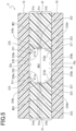
- Fig. 5 is a cross-sectional diagram illustrating an example configuration of a microfluidic chip 3 according to the second modified example of the present embodiment.
- the microfluidic chip 3 includes a substrate 10, a partition layer 31 that defines a fluidic channel portion 33 on the substrate 10, and a cover layer 12. As shown in Fig. 5 , the microfluidic chip 3 differs from the microfluidic chip 2 according to the first modified example described above in that a plurality of inclined surfaces (inclined surfaces 311 and 313 described later) are provided on a side surface 310 of the partition layer 31.
- partition layer 31 and the fluidic channel portion 33 defined by the partition layer 31 Components other than the partition layer 31 and the fluidic channel portion 33 (substrate 10 and cover layer 12) have the same configuration as the substrate 10 and the cover layer 12 of the microfluidic chip 1, and the description thereof will be omitted.
- the partition layer 31 of the microfluidic chip 3 has a shape in which a width W21 increases toward both the substrate 10 and the cover layer 12 in cross-sectional view.
- the areas of the bonding region for bonding the partition layer 31 and the cover layer 12 and the bonding region for bonding the partition layer 31 and the substrate 10 increase. Accordingly, in addition to the adhesion between the partition layer 31 and the cover layer 12, the adhesion between the partition layer 31 and the substrate 10 can be enhanced. This can reliably prevent occurrence of liquid leakage, damage, and the like during use of the microfluidic chip 3.
- cross-section in the “cross-sectional view” refers to a cross-section of the microfluidic chip 3 cut in the thickness direction (direction perpendicular to the longitudinal direction of the fluidic channel portion 33), for example, and the cross-section includes the substrate 10, the partition layer 31, the cover layer 12 and the fluidic channel portion 33.
- the shape of the partition layer 31 will be more specifically described.
- the partition layer 31 of the microfluidic chip 3 includes a side surface 310 that defines the fluidic channel portion 33.
- the side surface 310 is connected to the cover layer 12 at an upper end 310a which is an end on the cover layer 12 side. Further, the side surface 310 is connected to the substrate 10 at a lower end 310b which is an end on the substrate 10 side. As shown in Fig. 5 , the side surface 310 has an inclined surface 311 that is inclined relative to the cover layer 12 and an inclined surface 313 that is inclined relative to the substrate 10.
- the partition layer 31 of the microfluidic chip 3 differs from the partition layer 21 of the microfluidic chip 2 according to the first modified example in that the side surface 310 of the partition layer 31 has the inclined surface 311 and the inclined surface 313 at respective ends.
- the inclined surface 311 is provided on one end side of the side surface 310. Specifically, the inclined surface 311 is provided on an upper end 310a side of the side surface 310.
- the inclined surface 313 is provided on the other end side of the side surface 310. Specifically, the inclined surface 313 is provided on a lower end 310b side of the side surface 310. Further, a flat surface 312 is formed in a region of the side surface 310 in which the inclined surfaces (inclined surfaces 311 and 313) are not provided, that is, a region between the inclined surface 311 and the inclined surface 313.
- the flat surface 312 is connected to the inclined surface 311 at a first intermediate end 310c, and connected to the inclined surface 313 at a second intermediate end 311d. That is, the flat surface 312 extends from the first intermediate end 310c to the second intermediate end 310d of the side surface 310, with the first intermediate end 310c corresponding to the upper end of the flat surface 312 and the second intermediate end 310d corresponding to the lower end of the flat surface 312.
- the inclined surface 311 is connected to the cover layer 12 at the upper end 310a of the side surface 310, and connected to the flat surface 312 at the first intermediate end 310c of the side surface 310. That is, the inclined surface 311 extends from the upper end 310a to the first intermediate end 311c of the side surface 310, with the upper end 310a of the side surface 310 corresponding to the upper end of the inclined surface 311 and the first intermediate end 311c of the side surface 310 corresponding to the lower end of the inclined surface 311.
- the inclined surface 313 is connected to the flat surface 312 at the second intermediate end 310d of the side surface 310, and connected to the substrate 10 at the lower end 310b of the side surface 310. That is, the inclined surface 313 extends from the second intermediate end 310d to the lower end 310b of the side surface 310, with the second intermediate end 310d of the side surface 310 corresponding to the upper end of the inclined surface 313 and the lower end 310b of the side surface 310 corresponding to the lower end of the inclined surface 311.
- a region of the partition layer 31 including the inclined surface 311 is referred to as an upper region 31a
- a region including the inclined surface 313 is referred to as a lower region 31b
- a region including the flat surface 312 is referred to as an intermediate region 31c.
- the upper region 31a, the lower region 31b and the intermediate region 31c of the partition layer 31 are divided by a virtual dotted line for ease of understanding.
- the upper region 31a, the lower region 31b and the intermediate region 31c are preferably formed integrally, but may be formed separately. That is, the partition layer 31 may have a multilayer (e.g., three-layer) structure.
- the width W21 of the partition layer 31 increases toward the cover layer 12 in the upper region 31a which includes the inclined surface 311, increases toward the substrate 10 in the lower region 31b which includes the inclined surface 313, and is constant in the intermediate region 31c which includes the flat surface 212. Further, the width W21 of the partition layer 31 is smaller in the intermediate region 31c than in the other regions (upper region 31a, lower region 31b). With this configuration, the areas of the bonding region for bonding the partition layer 31 and the cover layer 12 and the bonding region for bonding the partition layer 31 and the substrate 10 can be increased, while maintaining the width (fluidic channel width W22) of the fluidic channel defined by the partition layer 31 in the microfluidic chip 3.
- the inclined surface 311 is formed on a part of the side surface 310 (side surface 310 of the upper region 31a of the partition layer 31) and curved in a concave shape in cross-sectional view.
- the inclined surface 311 provided on the side surface 310 of the partition layer 31 has the same configuration as the inclined surface 211 provided on the side surface 210 of the partition layer 21 in the microfluidic chip 2 according to the first modified example, but the partition layer 21 and the partition layer 31 are different in configuration, so the inclined surface 311 will be described below.
- the curved inclined surface 311 is provided on the side surface 310 of the partition layer 31, that is, on a region of the side surface 310 on the cover layer 12 side.
- the upper end 310a of the side surface 310 (upper end of the inclined surface 311) is located closer to the center of the fluidic channel portion 33 than the first intermediate end 310c (lower end of the inclined surface 311) is. That is, the upper end 310a of the side surface 310 (upper end of the inclined surface 311) is located closer to the opposing partition layer 31 than the first intermediate end 310c is.
- the first intermediate end 310c of the side surface 310 (lower end of the inclined surface 311) is located further away from the center of the fluidic channel portion 33 than the upper end 310a (upper end of the inclined surface 311) is. That is, the first intermediate end 310c of the side surface 310 (lower end of the inclined surface 311) is located further away from the opposing partition layer 31 than the upper end 310a is.
- the inclined surface 311 extends upward in an inclined manner from the first intermediate end 310c connected to the flat surface 312 to the upper end 310a, where it is connected to the cover layer 12.
- the width W21 of the partition layer 31 increases in the direction toward the center of the fluidic channel portion 33, that is, toward the opposing partition layer 31 (in the transverse direction of the fluidic channel portion 33), as it approaches the cover layer 12. Therefore, the width W21 of the partition layer 31 in cross-sectional view increases toward the cover layer 12.
- the width W21 of the upper region 31a of the partition layer 31 continuously increases toward the cover layer 12. More specifically, the width W21 of the upper region 31a continuously expands and increases toward the center of the fluidic channel portion 33, that is, in the transverse direction, as it approaches the cover layer 12.
- the “continuously increases (expands)” herein means that the width W21 of the partition layer 31 continuously increases (expands), without decreasing (reducing), from the first intermediate end 310c where the inclined surface 311 is connected to the flat surface 312 to the upper end 310a where the inclined surface 311 is connected to the cover layer 12.
- a deepest portion 311a is located closer to the center of the fluidic channel portion 33 than the first intermediate end 310c which is the lower end of the inclined surface 311 (upper end of the flat surface 312) is. Therefore, the width W21 of the partition layer 31 continuously increases, without decreasing, even in the deepest portion 311a of the inclined surface 311.
- the area of the bonding region for bonding the partition layer 31 and the cover layer 12 can be reliably increased, further reliably enhancing adhesion between the partition layer 31 and the cover layer 12.
- the partition layer 31 includes an extension portion 315 which includes the curved inclined surface 311 in the upper region 31a and extends in the transverse direction of the fluidic channel portion 33 along the surface (rear surface 12a) of the cover layer 12 on the fluidic channel portion 33 side.
- the extension portion 315 extends in the direction toward the center of the fluidic channel portion 33, that is, toward the opposing partition layer 31.
- the extension portion 315 has a shape in which the thickness decreases in the transverse direction of the fluidic channel portion 33. That is, the extension portion 315 has a flared shape.
- the microfluidic chip 3 can reduce a decrease in the width (fluidic channel width W22) of the fluidic channel portion 33 due to an increase in the width W21 of the partition layer 31, while increasing the area of the bonding region for bonding the partition layer 31 and the cover layer 12.
- the inclined surface 313 provided on the side surface 310 of the partition layer 31 will be described.
- the inclined surface 313 is formed on a part of the remaining side surface 310 (side surface 310 of the lower region 31b of the partition layer 31) and curved in a concave shape in cross-sectional view.
- the curved inclined surface 313 is provided on the side surface 310 of the lower region 31b of the partition layer 31, that is, on a region of the side surface 310 on the substrate 10 side.
- the lower end 310b of the side surface 310 (lower end of the inclined surface 313) is located closer to the center of the fluidic channel portion 33 than the second intermediate end 310d (upper end of the inclined surface 313) is. That is, the lower end 310b of the side surface 310 (lower end of the inclined surface 313) is located closer to the opposing partition layer 31 than the second intermediate end 310d is.
- the second intermediate end 310d of the side surface 310 (upper end of the inclined surface 313) is located further away from the center of the fluidic channel portion 33 than the lower end 310b (lower end of the inclined surface 313) is. That is, the second intermediate end 310d of the side surface 310 (upper end of the inclined surface 313) is located further away from the opposing partition layer 31 than the lower end 310b is.
- the inclined surface 313 extends downward in an inclined manner from the second intermediate end 310d connected to the flat surface 312 to the lower end 310b, where it is connected to the substrate 10.
- the width W21 of the partition layer 31 increases in the direction toward the center of the fluidic channel portion 33, that is, toward the opposing partition layer 31 (in the transverse direction of the fluidic channel portion 33), as it approaches the substrate 10. Therefore, the width W21 of the partition layer 31 in cross-sectional view increases toward the substrate 10.
- the width W21 of the lower region 31b of the partition layer 31 continuously increases toward the substrate 10. More specifically, the width W21 of the lower region 31b of the partition layer 21 continuously expands and increases toward the center of the fluidic channel portion 33, that is, in the transverse direction, as it approaches the substrate 10.
- the “continuously increases (expands)” herein means that the width W21 of the partition layer 31 continuously increases (expands), without decreasing (reducing), from the second intermediate end 310d where the inclined surface 313 is connected to the flat surface 312 to the lower end 310b where the inclined surface 313 is connected to the substrate 10.
- a deepest portion 313a is located closer to the center of the fluidic channel portion 33 than the second intermediate end 310d which is the upper end of the inclined surface 313 (lower end of the flat surface 312) is. Therefore, the width W21 of the partition layer 31 continuously increases, without decreasing, even in the deepest portion 313a of the inclined surface 313.
- the area of the bonding region for bonding the partition layer 31 and the substrate 10 can be reliably increased, further reliably enhancing adhesion between the partition layer 31 and the substrate 10.
- the partition layer 31 includes an extension portion 317 which includes the curved inclined surface 313 in the lower region 31b and extends in the transverse direction of the fluidic channel portion 33 along the front surface 10a of the substrate 10.
- the extension portion 317 extends in the direction toward the center of the fluidic channel portion 33, that is, toward the opposing partition layer 31.
- the extension portion 317 has a shape in which the thickness decreases in the transverse direction of the fluidic channel portion 33. That is, the extension portion 317 has a flared shape.
- the microfluidic chip 3 can reduce a decrease in the width (fluidic channel width W22) of the fluidic channel portion 33 due to an increase in the width W21 of the partition layer 31, while increasing the area of the bonding region for bonding the partition layer 31 and the substrate 10.
- the partition layer 31 includes the inclined surface 311 (an example of the first inclined surface) which is a curved inclined surface provided on a part of the side surface 310 and the inclined surface (an example of the second inclined surface) 313 which is provided on the remaining portion (portion in which the inclined surface 311 is not provided) of the side surface 310.
- the inclined surface 313 is curved in a concave shape in cross-sectional view, and one end of the inclined surface 313 is connected to the substrate 10.
- the flat surface 312 is provided on the side surface 310 between the inclined surface 311 and the inclined surface 313.
- the partition layer 31 has flared-shape portions respectively on the substrate 10 side and the cover layer 12 side. Accordingly, the partition layer 31 has a shape in which the width W21 increases toward both the substrate 10 and the cover layer 12
- the bonding region for bonding the partition layer 31 and the cover layer 12 and the bonding region for bonding the partition layer 31 and the substrate 10 increase. Therefore, the microfluidic chip 3 can enhance adhesion between the partition layer 31 and the cover layer 12 and adhesion between the partition layer 31 and the substrate 10, and can reliably prevent occurrence of liquid leakage, damage, and the like during use of the microfluidic chip 3.
- the inclined surface 311 and the inclined surface 313 may have the same shape or different shapes.
- the inclined surface 311 may be curved more deeply than the inclined surface 313 is, or the inclined surface 313 may be curved more deeply than the inclined surface 311 is.
- the deepest portion 311a of the inclined surface 311 may be located further away from the center of the fluidic channel portion 33 than the deepest portion 313a of the inclined surface 313 is, or the deepest portion 313a of the inclined surface 313 may be located further away from the center of the fluidic channel portion 33 than the deepest portion 311a of the inclined surface 311 is.
- the fluidic channel portion 33 has a fluidic channel width W22 defined as the width between a pair of partition layers 31 facing each other, that is, the width between the side surfaces 310.
- the width W21 of the partition layer 31 in cross-sectional view increases toward each of the substrate 10 and the cover layer 12.
- the width between the side surfaces 310 of the pair of partition layers 21 is narrower on the substrate 10 side and the cover layer 12 side than between the flat surfaces 312. Therefore, the fluidic channel width W22 of the fluidic channel portion 33 decreases from the center region in the height of the fluidic channel portion 33 (thickness of the partition layer 31) toward each of the substrate 10 and the cover layer 12.
- the fluidic channel width W22 is widest between the first intermediate ends 310c and between the second intermediate ends 310d of the side surfaces 310 of the pair of partition layers 31.
- the width W21 of the partition layer 31 is constant in the intermediate region 31c which includes the flat surface 312 extending from the first intermediate end 310c to the second intermediate end 310d of the side surface 310. Accordingly, the width between the flat surfaces 312 in the pair of partition layers 31 is constant. That is, the fluidic channel width W22 between the flat surfaces 312 (between the intermediate regions 31c) of the pair of partition layers 31 is constant. Therefore, the fluidic channel width W22 of the fluidic channel portion 33 is widest between the flat surfaces 312 of the side surfaces 310 of the pair of partition layers 31. That is, the fluidic channel width W22 of the fluidic channel portion 33 is widest in the region between the flat surfaces 312.
- the fluidic channel width W22 is narrowest at the bottom of the fluidic channel portion 33 where the front surface 10a of the substrate 10 is exposed, that is, between the lower ends 310b of the pair of partition layers 31, and at the top of the fluidic channel portion 33 where the rear surface 12a of the cover layer 12 is exposed, that is, between the upper ends 310a of the pair of partition layers 31.
- the width W21 of the partition layer 31 continuously increases toward the cover layer 12 in the upper region 31a which includes the inclined surface 311 extending from the first intermediate end 310c to the upper end 310a of the side surface 310. That is, in the pair of partition layers 31 facing each other, each of the extension portions 315, which include the inclined surface 311, approaches the other in the transverse direction of the fluidic channel portion 33. Therefore, the width between the inclined surfaces 311 of the pair of partition layers 31 becomes continuously narrower (decreases) toward the cover layer 12. That is, the fluidic channel width W22 between the inclined surfaces 311 (between the upper regions 31a) of the pair of partition layers 31 becomes continuously narrower (decreases) toward the cover layer 12.
- the “continuously decreases” herein means that the fluidic channel width W22 of the fluidic channel portion 33 continuously decreases, without increasing, from a region between the upper ends of the flat surfaces 312 (region between the first intermediate ends 310c of the pair of partition layers 31) toward the top of the fluidic channel portion 33 (between the upper ends 310a of the pair of partition layers 31).
- the width W21 of the partition layer 31 continuously increases toward the substrate 10 in the lower region 31b which includes the inclined surface 313 extending from the second intermediate end 310d to the lower end 310b of the side surface 310. That is, in the pair of partition layers 31 facing each other, each of the extension portions 317, which include the inclined surface 313, approaches the other in the transverse direction of the fluidic channel portion 33. Therefore, the width between the inclined surfaces 313 of the pair of partition layers 31 becomes continuously narrower (decreases) toward the substrate 10. That is, the fluidic channel width W22 between the inclined surfaces 313 (between the lower regions 31b) of the pair of partition layers 31 becomes continuously narrower (decreases) toward the substrate 10.
- the “continuously decreases” herein means that the fluidic channel width W22 of the fluidic channel portion 33 continuously decreases, without increasing, from a region between the lower ends of the flat surfaces 312 (region between the second intermediate ends 310d of the pair of partition layers 31) toward the bottom of the fluidic channel portion 33 (between the lower ends 310b of the pair of partition layers 31).
- the width of the fluidic channel portion 33 continuously decreases toward the cover layer 12 in a region including the inclined surface 311 (region formed by the inclined surface 311) of the side surface 310 of the partition layer 31. Further, the fluidic channel width W22 continuously decreases toward the substrate 10 in a region including the inclined surface 313 (region formed by the inclined surface 313) of the side surface 310 of the partition layer 31. Furthermore, the fluidic channel width W22 is constant in a region formed by the surface other than the inclined surface 311 and the inclined surface 313, that is, the flat surface 312 of the side surface 310 of the partition layer 31.
- a region with reduced fluidic channel width W22 can be limited to a region on the top side (cover layer 12 side) of the fluidic channel portion 33, that is, between the inclined surfaces 311 and a region on the bottom side (substrate 10 side) of the fluidic channel portion 33, that is, between the inclined surfaces 313. Accordingly, in the microfluidic chip 3, the areas of the bonding region for bonding the partition layer 31 and the cover layer 12 and the bonding region for bonding the partition layer 31 and the substrate 10 can be reliably increased, while maintaining the width of the fluidic channel width W22 of the fluidic channel portion 33 in a region between the flat surfaces 212 of the pair of partition layers 21.
- the microfluidic chip 2 can reliably enhance adhesion between the partition layer 31 and the cover layer 12 and between the partition layer 31 and the substrate 10, while improving flow stability of a fluid (e.g., reaction solution) in the fluidic channel portion 33 and visibility during observation of the interior of the fluidic channel portion 33.
- a fluid e.g., reaction solution
- the fluidic channel portion 33 has a rounded corner shape in cross-sectional view.
- the "cross-section” in the “cross-sectional view” refers to a cross-section of the microfluidic chip 3 cut in the thickness direction (direction perpendicular to the longitudinal direction of the fluidic channel portion 33), and the cross-section includes the substrate 10, the partition layer 31, the cover layer 12 and the fluidic channel portion 33. Since the fluidic channel portion 33 has a rounded corner shape in cross-sectional view, a fluid flow speed and a flow rate of a fluid (e.g., reaction solution) in the fluidic channel portion 33 can be stabilized.
- a fluid e.g., reaction solution
- the shape of the partition layer 31 and the configuration of the fluidic channel portion 33 in the microfluidic chip 3 according to this modified example has been described.
- the basic configuration such as materials other than the shape of the partition layer 31, the thickness (fluidic channel height), and the width and fluidic channel length of the fluidic channel portion 33 are the same as those of the partition layer 11 and the fluidic channel portion 3 of the microfluidic chip 1 according to the first embodiment, and the description thereof will be omitted.
- the basic method of producing a microfluidic chip 3 according to this modified example is the same as the method of producing a microfluidic chip 1 according to the first embodiment described above (see Fig. 2 ), and detailed description will be omitted.
- the upper and lower parts of the partition layer 31 can be formed in a flared shape by adjusting the wavelength of ultraviolet light during exposure (adjusting the exposure light for exposing the photosensitive resin to the above specific wavelength range in the ultraviolet light region) in the exposure step (step S3) and removing excess resin from the photosensitive resin layer in the development step (step S4). Accordingly, the partition layer 31 can be formed to have a width which increases toward each of the substrate 10 and the cover layer 12.
- the inclined surface 311 in the microfluidic chip 3 according to this modified example may be formed in the same manner as with the inclined surface 211 in the microfluidic chip 2 according to the first modified example. That is, in the exposure step (step S3), curing of the resin (in this example, negative resist) in the upper part of the photosensitive resin layer progresses, increasing the amount of resin that remains without being dissolved during development, whereby the width W21 of the partition layer 31 in the upper region 31a of the partition layer 31 can be increased toward the cover layer 12. Further, the inclined surface 311 curved in a concave shape in cross-sectional view with one end (upper end 310a) being in contact with the cover layer 12 can be formed by development.
- the resin in this example, negative resist
- the amount of exposure in the upper part of the photosensitive resin layer can be the same as that in the lower part (on the substrate 10 side). Accordingly, the amount of resin that remains without being dissolved during development in the upper and lower parts of the photosensitive resin layer increases. On the other hand, more resin is dissolved during development in the intermediate portion of the photosensitive resin layer where the amount of exposure is low, compared with the upper and lower parts, resulting in a smaller amount of resin remaining.
- the width W21 of the upper region 31a of the partition layer 31 can be increased toward the cover layer 12, and the width W21 of the lower region 31b of the partition layer 31 can be increased toward the substrate 10. Further, the width W21 of the partition layer 31 can be smaller in the intermediate region 31c of the partition layer 31 than in each of the upper region 31a and the lower region 31b.
- the inclined surface 311 can be formed on the side surface 310 of the upper region 31a of the partition layer 31.
- the inclined surface 313 can be formed on the side surface 310 of the lower region 31b of the partition layer 31.
- the inclined surfaces 311 and 313 can be formed in a curved shape in cross-sectional view by adjusting, for example, the development time and the concentration of the developer in development.
- the flat surface 312 can be formed on the side surface 310 of the intermediate region 31c of the partition layer 31.
- the partition layer formed of the photosensitive resin layer may have a bilayer structure of a positive resist and a negative resist. Specifically, a positive resist is applied to the substrate 10, exposed and developed to form a lower flared-shape portion (lower region 31b). Then, a negative resist is applied to the lower flared-shape portion, exposed and developed to form an upper flared-shape portion (upper region 31a). Thus, the partition layer 31 may have a bilayer structure.
- the closer to the substrate 10 the lower the amount of exposure and the less the resin dissolves, and the closer to the substrate 10, the greater the amount of resin remaining during development.
- the upper region 31a in the region of the photosensitive resin layer formed of the negative resist on the cover layer 12 side, the closer to the top, the higher the amount of exposure and the more the resin cures, and the closer to the top to which the cover layer 12 is bonded, the greater the amount of resin remaining.
- the width W21 of the upper region 31a of the partition layer 31 on the cover layer 12 side can be increased toward the cover layer 12, and the width W21 of the lower region 31b of the partition layer 31 on the substrate 10 side can be increased toward the substrate 10 (the upper and lower parts of the partition layer can be formed in a flared shape).
- the curved inclined surface 313 can be formed by development in the upper region 31a of the partition layer 31, and the curved inclined surface 313 can be formed in the lower region 31b.
- the flat surface 312 can be formed by development on the side surface 310 of the intermediate region 31c of the partition layer 31.
- step S3 the photosensitive resin is exposed to light having a wavelength of 250 nm or greater and 350 nm or less in the ultraviolet light region.
- the inclined surface 311 curved in a concave shape in cross-sectional view with one end (lower end 310b) being in contact with the substrate 10 is formed by development on a part of the side surface 310 of the partition layer 31 (side surface 310 of the lower region 31b).
- the second inclined surface curved in a concave shape in cross-sectional view with one end (upper end 310a) being in contact with the cover layer 12 is formed by development on the remaining portion of the side surface 310 of the partition layer 31 (side surface 310 of the upper region 31a).
- the microfluidic chip 3 can be obtained in which the areas of the bonding region for bonding the partition layer 31 and the substrate 10 and the bonding region for bonding the partition layer 31 and the cover layer 12 can be increased, enhancing adhesion between the partition layer 31 and the substrate 10 and adhesion between the partition layer 31 and the cover layer 12.
- FIG. 6 is a cross-sectional diagram illustrating an example configuration of a microfluidic chip 100 according to the second embodiment of the present disclosure.
- the microfluidic chip 100 includes a substrate 10, an adhesive layer 15 disposed on the substrate 10, a partition layer 11 that defines a fluidic channel portion 13 on the substrate 10, and a cover layer 12. That is, the microfluidic chip 100 differs from the microfluidic chip 1 according to the first embodiment in that the adhesive layer 15 is provided between the partition layer 11 and the substrate 10.
- the adhesive layer 15 will be described below. Components other than the adhesive layer 15 (substrate 10, partition layer 11, cover layer 12 and fluidic channel portion 13) have the same configuration as in the microfluidic chip 1, so the same reference signs are used and the description thereof will be omitted.
- the substrate 10 may be subjected to hydrophobic surface treatment (HMDS treatment) or may be coated with a thin film of resin in order to enhance adhesion between the substrate 10 and a resin layer (for example, photosensitive resin layer), that is, the partition layer 11.
- HMDS treatment hydrophobic surface treatment
- the adhesive layer 15 formed of a thin film may be provided between the substrate 10 and the partition layer 11 (photosensitive resin layer) as shown in Fig. 6 .
- a fluid for example, liquid
- the adhesive layer 15 provided on the substrate 10 can contribute to improving the resolution of the fluidic channel pattern of the photosensitive resin.
- FIG. 7 is a schematic cross-sectional diagram illustrating an example configuration of the microfluidic chip 200 according to this modified example.
- the microfluidic chip 200 has a configuration in which an adhesive layer is added to the microfluidic chip 2 according to the first modified example of the first embodiment.
- the microfluidic chip 200 includes a substrate 10, an adhesive layer 15 disposed on the substrate 10, a partition layer 21 that defines a fluidic channel portion 23 on the substrate 10, and a cover layer 12. That is, the microfluidic chip 200 differs from the microfluidic chip 2 according to the first modified example of the first embodiment in that the adhesive layer 15 is provided between the partition layer 21 and the substrate 10.
- the adhesive layer 15 in this modified example is the same as the adhesive layer 15 in the microfluidic chip 100 according to the second embodiment described above, and the description thereof will be omitted.
- Providing the adhesive layer 15 can enhance the adhesion between the substrate 10 and a resin layer (for example, photosensitive resin layer), that is, the partition layer 21 in the microfluidic chip 200.
- FIG. 8 is a schematic cross-sectional diagram illustrating an example configuration of the microfluidic chip 300 according to this modified example.
- the microfluidic chip 300 has a configuration in which an adhesive layer is added to the microfluidic chip 3 according to the second modified example of the first embodiment.
- the microfluidic chip 300 includes a substrate 10, an adhesive layer 15 disposed on the substrate 10, a partition layer 31 that defines a fluidic channel portion 33 on the substrate 10, and a cover layer 12. That is, the microfluidic chip 300 differs from the microfluidic chip 2 according to the second modified example of the first embodiment in that the adhesive layer 15 is provided between the partition layer 31 and the substrate 10.
- the adhesive layer 15 in this modified example is the same as the adhesive layer 15 in the microfluidic chip 100 according to the second embodiment described above, and the description thereof will be omitted.
- Providing the adhesive layer 15 can enhance the adhesion between the substrate 10 and a resin layer (for example, photosensitive resin layer), that is, the partition layer 31 in the microfluidic chip 300.
- the present disclosure can be suitably used for microfluidic chips for research applications, diagnostic applications, testing, analysis, culture, and the like, which do not require complicated production processes to form a top lid, and methods of producing the same.
Landscapes
- Chemical & Material Sciences (AREA)
- Health & Medical Sciences (AREA)
- Analytical Chemistry (AREA)
- General Health & Medical Sciences (AREA)
- Dispersion Chemistry (AREA)
- Hematology (AREA)
- Clinical Laboratory Science (AREA)
- Chemical Kinetics & Catalysis (AREA)
- Physics & Mathematics (AREA)
- Life Sciences & Earth Sciences (AREA)
- Biochemistry (AREA)
- General Physics & Mathematics (AREA)
- Immunology (AREA)
- Pathology (AREA)
- Physical Or Chemical Processes And Apparatus (AREA)
- Micromachines (AREA)
- Automatic Analysis And Handling Materials Therefor (AREA)
Abstract
Description
- The present disclosure relates to microfluidic chips and methods of producing the same.
- In recent years, technologies have been proposed in which micro reaction fields are formed by applying lithography processing or thick film processing technologies to enable testing in units of several microliters to several nanoliters. Technologies using such a micro reaction field are called µ-TAS (micro total analysis systems).
- µ-TAS is applied to fields such as genetic testing, chromosome testing, cell testing and drug development, biotechnologies, testing of trace substances in the environment, investigation of breeding environments for agricultural products, genetic testing of agricultural products, and the like. The introduction of µ-TAS technologies brings significant effects such as automation, higher speed, higher accuracy, lower cost, speed, reduced environmental impact, and the like.
- In µ-TAS, micrometer-sized fluidic channels (micro fluidic channels, micro channels) formed on a substrate are often used, and such a substrate is called a chip, microchip, microfluidic chip, or the like.
- Conventionally, such microfluidic chips have been produced using techniques such as injection molding, molding, cutting, etching, and the like. As the substrates of microfluidic chips, glass substrates are typically used since they are easy to produce and suitable for optical detection. Meanwhile, microfluidic chips using resin materials, which are lightweight, less likely to break than glass substrates, and inexpensive, are being developed. As a method of producing a microfluidic chip using a resin material, a resin pattern for a fluidic channel is formed typically by photolithography, and a lid material is bonded thereto to form a microfluidic chip. According to this method, microfluidic channel patterns, which have been sometimes difficult to produce with conventional techniques, can be formed.
- Such microfluidic chips are formed by bonding a plurality of members together. For example,
PTL 1 discloses a microfluidic chip produced by bonding members together via an adhesive. Further, as described inPTL 2 for example, a method has been proposed in which a process gas is turned into plasma at or near atmospheric pressure to modify a substrate surface, and members are bonded together without using an adhesive (e.g., PTL 2). -
- PTL 1:
JP 2007-240461 A - PTL 2:
JP 2011-104886 A - As the recent fluidic channel pattern structures have become more complex, the surface area of the fluidic channel portion (space portion) in microfluidic chips increases, inevitably reducing a region (bonding region) for bonding the wall and the lid material (cover member). Even for microfluidic chips having a complex fluidic channel pattern, there is a need to enhance adhesion between the wall and the lid material from the perspective of preventing occurrence of liquid leakage, damage, and the like during use.
- In view of the above problems, the present disclosure has been made to provide a microfluidic chip that can enhance adhesion between the wall and the lid material, and a method of producing the microfluidic chip.
- In order to solve the above problems, a microfluidic chip according to an aspect of the present disclosure includes: a substrate; a partition member made of a resin material, the partition member being disposed on the substrate and defining a fluidic channel; and a cover member disposed on a side of the partition member opposite to that facing the substrate, the cover member covering the fluidic channel, wherein the partition member has a width which increases toward the cover member in cross-sectional view.
- A method of producing a microfluidic chip according to another aspect of the present disclosure includes the steps of: applying a resin to a substrate; exposing the applied resin to light; subjecting the exposed resin to development and cleaning to thereby form a partition member that defines a fluidic channel on the substrate; post-baking the partition member; and bonding a cover member to a side of the partition member opposite to that facing the substrate, wherein in the step of exposing the resin, the photosensitive resin is exposed to light having a wavelength of 250 nm or greater and 350 nm or less in the ultraviolet light region, and excess resin on the substrate is removed by the development, whereby the partition member is formed to have a width which increases toward the cover member in cross-sectional view.
- According to the aspects of the present disclosure, a microfluidic chip that can enhance adhesion between the wall and the lid material can be provided.
-
-
Fig. 1 is a schematic diagram illustrating an example configuration of a microfluidic chip according to a first embodiment of the present disclosure, in which (a) is a schematic plan view of an example configuration of a microfluidic chip according to a first embodiment of the present disclosure, and (b) is a schematic cross-sectional diagram of an example configuration of a microfluidic chip according to a first embodiment of the present disclosure. -
Fig. 2 is a flowchart showing an example method of producing a microfluidic chip according to the first embodiment of the present disclosure. -
Fig. 3 is a line graph showing an example of light transmittance of a photosensitive resin layer. -
Fig. 4 is a schematic cross-sectional diagram illustrating an example configuration of a microfluidic chip according to a first modified example of the first embodiment of the present disclosure. -
Fig. 5 is a schematic cross-sectional diagram illustrating an example configuration of a microfluidic chip according to a second modified example of the first embodiment of the present disclosure. -
Fig. 6 is a schematic cross-sectional diagram illustrating an example configuration of a microfluidic chip according to a second embodiment of the present disclosure. -
Fig. 7 is a schematic cross-sectional diagram illustrating an example configuration of a microfluidic chip according to a first modified example of the second embodiment of the present disclosure. -
Fig. 8 is a schematic cross-sectional diagram illustrating an example configuration of a microfluidic chip according to a second modified example of the second embodiment of the present disclosure. - The present disclosure will be described through embodiments, but the following embodiments do not limit the invention defined in the appended claims. Further, not all of the combinations of features described in the embodiments are essential for the solution of the invention. The drawings schematically illustrate the invention defined in the appended in the claims, and dimensions such as the width, thickness, and the like of each component may differ from the actual ones, and the ratios thereof may also differ from the actual ones.
- The following description will be given of a microfluidic chip according to a first embodiment of the present disclosure. In the following description, a substrate side of the microfluidic chip may be referred to as "lower side", and a side (lid material side) of the microfluidic chip opposite to that facing the substrate may be referred to as "upper side".
- The inventors of the present invention have diligently studied and found that, in microfluidic chips, the area of the bonding region for bonding a wall and a lid material to each other can be increased by forming the wall into a specific shape. Accordingly, the inventors have invented a microfluidic chip which can enhance adhesion strength between the wall and the lid material, and a method of producing the microfluidic chip.
- With reference to the drawings, embodiments of the present disclosure will be described below.
-
Fig. 1 is a schematic diagram illustrating an example configuration of amicrofluidic chip 1 according to a first embodiment of the present disclosure (hereinafter, also referred to as "the present embodiment"). Specifically,Fig. 1(a) is a schematic plan view of themicrofluidic chip 1 of the present embodiment.Fig. 1(b) is a schematic cross-sectional diagram illustrating a cross-section of themicrofluidic chip 1 taken along the line A-A inFig. 1(a) . - As shown in
Fig. 1(a) , themicrofluidic chip 1 includes aninlet 4 for introducing a fluid (for example, liquid), afluidic channel portion 13 through which the fluid introduced through theinlet 4 flows, and anoutlet 5 for discharging the fluid from thefluidic channel portion 13. In themicrofluidic chip 1, thefluidic channel portion 13 is covered with acover layer 12, and theinlet 4 and theoutlet 5 are through holes formed in thecover layer 12. Details of thecover layer 12 will be described later. -
Fig. 1(a) shows thefluidic channel portion 13 as seen through thetransparent cover layer 12. - In the
microfluidic chip 1, at least oneinlet 4 and at least oneoutlet 5 may be provided, and a plurality of each may be provided. Further, in themicrofluidic chip 1, a plurality offluidic channel portions 13 may be provided, and thefluidic channel portions 13 may be designed to merge or branch the fluid introduced from theinlet 4. - In the following description, details of the members constituting the
fluidic channel portion 13 in themicrofluidic chip 1 will be described. As shown inFig. 1(b) , themicrofluidic chip 1 includes asubstrate 10, a partition layer (an example of partition member) 11 provided on thesubstrate 10 and defining the fluidic channel, and a cover layer (an example of cover member) 12 provided on a side of thepartition layer 11 opposite to that facing thesubstrate 10 and covering thefluidic channel portion 13. Thefluidic channel portion 13 through which the fluid introduced from theinlet 4 flows is a region surrounded by thesubstrate 10, thepartition layer 11 and thecover layer 12. Thefluidic channel portion 13 is defined by a pair ofpartition layers 11 facing each other provided on thesubstrate 10, and a side of thefluidic channel portion 13 opposite to that facing thesubstrate 10 is covered with thecover layer 12 as a lid material. As described above, a fluid is introduced into thefluidic channel portion 13 from the inlet 4 (seeFig. 1(a) ) formed in thecover layer 12, and the fluid that has flowed through thefluidic channel portion 13 is discharged from theoutlet 5. - Although details will be described later, the
partition layer 11 in the present embodiment has a width W1 that increases toward thecover layer 12 in cross-sectional view. That is, the width W1 of thepartition layer 11 in cross-sectional view increases toward thecover layer 12. With this configuration, in themicrofluidic chip 1, the area of the bonding region for bonding the wall (partition layer 11) and the lid material (cover layer 12) can be increased, enhancing adhesion between thepartition layer 11 and thecover layer 12. - The
substrate 10 is a member that serves as a base of themicrofluidic chip 1, and thepartition layer 11 provided on thesubstrate 10 defines thefluidic channel portion 13. That is, thesubstrate 10 and thepartition layer 11 can be regarded as a main body of themicrofluidic chip 1. - The
substrate 10 can be made of either a translucent material or a non-translucent material. For example, when the state inside the fluidic channel portion 13 (state of fluid) is detected and observed using light, a material having excellent transparency to the light can be used. As the translucent material, resin, glass, or the like can be used. Examples of the resin used for the translucent material constituting thesubstrate 10 include acrylic resin, methacrylic resin, polypropylene, polycarbonate resin, cycloolefin resin, polystyrene resin, polyester resin, urethane resin, silicone resin and fluororesin from the viewpoint of being suitable for forming the main body of themicrofluidic chip 1. - Further, for example, when the state inside the fluidic channel portion 13 (state of fluid) is not necessarily detected and observed using light, a non-translucent material may be used. Examples of the non-translucent material include silicon wafers and copper plates. Although the thickness of the
substrate 10 is not particularly limited, it is preferably in the range of 10 µm (0.01 mm) or greater and 10 mm or less since a certain degree of rigidity is required in formation of a fluidic channel. - The
partition layer 11 is disposed on the substrate and forms afluidic channel portion 13. Thepartition layer 11 can be made of a resin material. Examples of the resin material of thepartition layer 11 include a photosensitive resin. - The photosensitive resin constituting the
partition layer 11 is preferably photosensitive to light having a wavelength of 190 nm or greater and 400 nm or less, which is in the ultraviolet light region. As the photosensitive resin, a photoresist such as liquid resist or dry film resist can be used. The photosensitive resin may be either positive type in which the photosensitive region dissolves or negative type in which the photosensitive region becomes insoluble. Examples of the photosensitive resin composition suitable for forming thepartition layer 11 in themicrofluidic chip 1 include radical negative type photosensitive resins containing alkali-soluble polymers, addition polymerizable monomers and photopolymerization initiators. Examples of the photosensitive resin material include acrylic resins, acrylic urethane resins (urethane acrylate resins), epoxy resins, polyamide resins, polyimide resins, polyurethane resins, polyester resins, polyether resins, polyolefin resins, polycarbonate resins, polystyrene resins, norbornene resins, phenol novolac resins, and other photosensitive resins, and these can be used singly, or in combinations or as copolymers of two or more. - In the present embodiment, the resin material of the
partition layer 11 is not limited to a photosensitive resin, and may be, for example, silicone rubber (PDMS: polydimethylsiloxane) or synthetic resin. Examples of the synthetic resin include polymethyl methacrylate resin (PMMA), polycarbonate (PC), polystyrene resin (PS), polypropylene (PP), cycloolefin polymer (COP) and cycloolefin copolymer (COC). The resin material of thepartition layer 11 is preferably selected as appropriate according to the application. - Further, the thickness of the
partition layer 11 on thesubstrate 10, that is, the height of thefluidic channel portion 13, is not particularly limited, but is required to be greater than the substances to be analyzed or inspected (for example, drugs, bacteria, cells, red blood cells, leukocytes, etc.) contained in the fluid introduced into thefluidic channel portion 13. Therefore, the thickness of thepartition layer 11, that is, the height of thefluidic channel portion 13, is preferably in the range of 5 µm or greater and 100 µm or less. - Similarly, since the width of the
fluidic channel portion 13 is required to be greater than the substances to be analyzed or inspected, the width of thefluidic channel portion 13 defined by thepartition layer 11 is preferably in the range of 5 µm or greater and 100 µm or less. - Further, in order to ensure sufficient reaction time for the reaction solution, the length of the fluidic channel defined by the
partition layer 11 is preferably in the range of 10 mm or greater and 100 mm or less, more preferably in the range of 30 mm or greater and 70 mm or less, and still more preferably in the range of 40 mm or greater and 60 mm or less. - In the
microfluidic chip 1 in the present embodiment, thecover layer 12 is a lid material covering thefluidic channel portion 13 as shown inFig. 1(b) . As described above, thecover layer 12 is provided on a side of thepartition layer 11 opposite to that facing thesubstrate 10, and thecover layer 12 faces thesubstrate 10 with thepartition layer 11 therebetween. More specifically, as shown inFig. 1(b) , thecover layer 12 in cross-sectional view has side portions supported by thepartition layer 11 and a center region that faces thesubstrate 10, the center region defining the upper side of thefluidic channel portion 13. - The
cover layer 12 can be made of either a translucent material or a non-translucent material For example, when the state inside the fluidic channel is detected and observed using light, a material having excellent transparency to the light can be used. As the translucent material, resin, glass, or the like can be used. Examples of the resin constituting thecover layer 12 include acrylic resin, methacrylic resin, polypropylene, polycarbonate resin, cycloolefin resin, polystyrene resin, polyester resin, urethane resin, silicone resin and fluororesin from the viewpoint of being suitable for forming the main body of themicrofluidic chip 1. The thickness of thecover layer 12 is not particularly limited, but in view of forming through holes corresponding to theinlet 4 and theoutlet 5 in thecover layer 12, it is preferably in the range of 10 µm or greater and 10 mm or less. Further, it is also preferred that holes corresponding to theinlet 4 for introducing a fluid (liquid) and theoutlet 5 for discharging a fluid are formed in advance in thecover layer 12 before thecover layer 12 is bonded to thepartition layer 11. - In the following description, details of the shape of the
partition layer 11 and the configuration of thefluidic channel portion 13 in themicrofluidic chip 1 according to the present embodiment will be described. First, the shape of thepartition layer 11 that defines thefluidic channel portion 13 will be described. - As shown in
Fig. 1(b) , the width W1 of thepartition layer 11 of themicrofluidic chip 1 increases toward thecover layer 12 in cross-sectional view. The "cross-section" in the "cross-sectional view" refers to a cross-section of themicrofluidic chip 1 cut in the thickness direction (direction perpendicular to the longitudinal direction of the fluidic channel portion 13), for example, and the cross-section includes at least thepartition layer 11, thecover layer 12 and thefluidic channel portion 13. - In the
microfluidic chip 1, the width W1 of thepartition layer 11 increases toward thecover layer 12, whereby the area of the bonding region for bonding thepartition layer 11 and thecover layer 12 can be increased, enhancing adhesion between thepartition layer 11 and thecover layer 12. This can prevent occurrence of liquid leakage, damage, and the like during use of themicrofluidic chip 1. In the following description, the shape of thepartition layer 11 will be more specifically described. - The
partition layer 11 of themicrofluidic chip 1 includes aside surface 110 that defines thefluidic channel portion 13. Theside surface 110 is connected to thecover layer 12 at anupper end 110a which is an end on thecover layer 12 side. Further, theside surface 110 is connected to thesubstrate 10 at alower end 110b which is an end on thesubstrate 10 side. As shown inFig. 1(b) , theside surface 110 has aninclined surface 111 that is inclined relative to thecover layer 12. - The
inclined surface 111 will be specifically described below. As shown inFig. 1(b) , theinclined surface 111 has a planar shape. Further, in thepartition layer 11 of themicrofluidic chip 1 according to the present embodiment, theinclined surface 111 is provided on theentire side surface 110. More specifically, theinclined surface 111 extends from theupper end 110a to thelower end 110b of theside surface 110, and is connected to thecover layer 12 at theupper end 110a of theside surface 110 and to thesubstrate 10 at thelower end 110b. That is, theupper end 110a is the upper end of theside surface 110 and theinclined surface 111, and thelower end 110b is the lower end of theside surface 110 and theinclined surface 111. - As shown in
Fig. 1(b) , in thepartition layer 11, theupper end 110a of the side surface 110 (upper end of the inclined surface 111) is located closer to the center of thefluidic channel portion 13 than thelower end 110b is. That is, theupper end 110a of the side surface 110 (upper end of the inclined surface 111) is located closer to the opposingpartition layer 11 than thelower end 110b is. In other words, in thepartition layer 11, thelower end 110b of the side surface 110 (lower end of the inclined surface 111) is located further away from the center of thefluidic channel portion 13 than theupper end 110a is. That is, thelower end 110b of the side surface 110 (lower end of the inclined surface 111) is located further away from the opposingpartition layer 11 than theupper end 110a is. - The
inclined surface 111 extends upward in an inclined manner from thelower end 110b connected to thecover layer 12 to theupper end 110a, where it is connected to thecover layer 12. Thus, the width W1 of thepartition layer 11 in cross-sectional view increases in the direction toward the center of thefluidic channel portion 13, that is, toward the opposingpartition layer 11 in the transverse direction of thefluidic channel portion 13, as it approaches thecover layer 12. Therefore, the width W1 of thepartition layer 11 in cross-sectional view increases from thesubstrate 10 side toward thecover layer 12 side. - As described above, the
inclined surface 111 has a planar shape and is provided on theentire side surface 110 of thepartition layer 11. Thus, the width W1 of thepartition layer 11 continuously increases toward thecover layer 12. Specifically, the width W1 of thepartition layer 11 continuously expands and increases toward the center of the fluidic channel portion 13 (in the transverse direction), as it approaches thecover layer 12. The "continuously increases (expands)" herein means that the width W1 of thepartition layer 11 continuously increases (expands), without decreasing (reducing), from the lower end 110ba where theinclined surface 111 is connected to thesubstrate 10 to theupper end 110a where theinclined surface 111 is connected to thecover layer 12substrate 10. With this configuration, in themicrofluidic chip 1, the area of the bonding region for bonding thepartition layer 11 and thecover layer 12 can be reliably increased, further reliably enhancing adhesion between thepartition layer 11 and thecover layer 12. - Next, the configuration of the
fluidic channel portion 13 defined by thesubstrate 10, thepartition layer 11 and thecover layer 12 will be described. - The
fluidic channel portion 13 has a fluidic channel width W2 defined as the width between a pair of partition layers 11 facing each other, that is, the width between the side surfaces 110. In the present embodiment, theinclined surface 111 is provided on theentire side surface 110, so the fluidic channel width W2 can also be defined as the width between the inclined surfaces 111. As described above, the width W1 of thepartition layer 11 in cross-sectional view increases toward thecover layer 12. As shown inFig. 1(b) , the width between theinclined surfaces 111 of the pair of partition layers 11 is narrower on thecover layer 12 side than on thesubstrate 10 side. Therefore, the fluidic channel width W2 of thefluidic channel portion 13 decreases from thesubstrate 10 side toward thecover layer 12 side. More specifically, the fluidic channel width W2 is widest at the lowest part (bottom) of thefluidic channel portion 13 where afront surface 10a of thesubstrate 10 is exposed, that is, between the lower ends 110b of the pair of partition layers 11. Further, the fluidic channel width W2 is narrowest at the top of thefluidic channel portion 13 where the cover layer 12 (specifically, arear surface 12a of the cover layer 12) is exposed, that is, between the upper ends 110a of the pair of partition layers 11. - As described above, since the
inclined surface 111 provided on theentire side surface 110 of thepartition layer 11 has a planar shape, the width W1 of thepartition layer 11 continuously increases toward thecover layer 12. That is, the width W1 increases in the transverse direction of thefluidic channel portion 13 as it approaches thecover layer 12 such that each of the pair of opposing partition layers 11 approaches the other. - Therefore, the width between the
inclined surfaces 111 of the pair of partition layers 11 becomes continuously narrower (decreases) toward thecover layer 12. Accordingly, the fluidic channel width W2 of thefluidic channel portion 13 becomes continuously narrower (decreases) toward thecover layer 12. More specifically, the fluidic channel width W2 continuously decreases from the lowest part (bottom) of thefluidic channel portion 13 where thesubstrate 10 is exposed toward the top of thefluidic channel portion 13 where the cover layer 12 (specifically, therear surface 12a) is exposed. - The "continuously decreases" herein means that the fluidic channel width W2 of the
fluidic channel portion 13 continuously decreases, without increasing, from the bottom of thefluidic channel portion 13 toward the top of thefluidic channel portion 13. Thus, as shown inFig. 1(b) , thefluidic channel portion 13 has a trapezoidal shape in cross-sectional view. The "cross-section" in the "cross-sectional view" refers to a cross-section of themicrofluidic chip 1 cut in the thickness direction (direction perpendicular to the longitudinal direction of the fluidic channel portion 13), and the cross-section includes thesubstrate 10, thepartition layer 11, thecover layer 12 and thefluidic channel portion 13. - As the width W1 of the
partition layer 11 continuously increases toward thecover layer 12, the fluidic channel width W2 of thefluidic channel portion 13 continuously decreases toward thecover layer 12. With this configuration, in themicrofluidic chip 1, the area of the bonding region for bonding thepartition layer 11 and thecover layer 12 can be reliably increased, further reliably enhancing adhesion between thepartition layer 11 and thecover layer 12. - In the
microfluidic chip 1 according to the present embodiment, thefluidic channel portion 13 includes abubble trapping region 130 that traps air bubbles in thefluidic channel portion 13. As shown inFig. 1(b) , thebubble trapping region 130 is formed by theinclined surface 111 of thepartition layer 11 and thefront surface 10a, which is the surface of thesubstrate 10 on thefluidic channel portion 13 side. - Air bubbles may be present in the
fluidic channel portion 13, for example, due to entrainment of air bubbles during injection of a fluid such as a reaction solution into themicrofluidic chip 1, boiling due to heating of the reaction solution, air entrainment due to nonuniform flow in the microfluidic channel, foaming from the reaction solution itself, or the like. - As shown in
Fig. 1(b) , in themicrofluidic chip 1, the fluidic channel width W2 of thefluidic channel portion 13 decreases toward thecover layer 12. Therefore, if the above air bubbles drift in thefluidic channel portion 13, especially in a center region E1 of thefluidic channel portion 13, which is the region near the center, fluid flow may become unstable, or visibility of the liquid may be reduced when the interior of thefluidic channel portion 13 is observed through thecover layer 12 or thesubstrate 10. - In the
microfluidic chip 1 according to the present embodiment, in which thebubble trapping region 130 is provided in thefluidic channel portion 13, air bubbles can be retained in a specific region (region other than the center region E1) in thefluidic channel portion 13. With this configuration, fluid flow can be stabilized and visibility during observation of the interior of thefluidic channel portion 13 can be improved. - As shown in
Fig. 1(b) , in themicrofluidic chip 1 according to the present embodiment, thebubble trapping region 130 is a recess formed by the inclined surface 111 (side surface 110) of thepartition layer 11 and thefront surface 10a of thesubstrate 10, and thelower end 110b of theinclined surface 111 is the deepest portion. More specifically, thebubble trapping region 130 is a corner formed by theinclined surface 111 of thepartition layer 11 and thefront surface 10a of thesubstrate 10 connected to each other at thelower end 110b of theinclined surface 111. That is, thebubble trapping region 130 is formed on each of the left and right sides of the lowest part (bottom) of the fluidic channel at which the fluidic channel width W2 of thefluidic channel portion 13 is widest. Therefore, by evacuating air bubbles into thebubble trapping region 130, the air bubbles can be retained in a region away from the center region E1 of thefluidic channel portion 13. With this configuration, themicrofluidic chip 1 according to the present embodiment can further stabilize fluid flow and further improve the visibility during observation of the interior of thefluidic channel portion 13. - Air bubbles in the
fluidic channel portion 13 migrate in the fluid (e.g., reaction solution) from the center region E1 toward the left and right sides of thefluidic channel portion 13 due to pressure or the like when the fluid flows, and are collected in thebubble trapping regions 130. In this example, the interior angle of thebubble trapping region 130 which is formed as a corner is an acute angle (less than 90 degrees). Accordingly, air bubbles collected in thebubble trapping region 130 are likely to remain in thebubble trapping region 130, and are less likely to leave (return) toward the center region E1 of thechannel portion 13. - As described above, the
microfluidic chip 1 according to the present embodiment includes thesubstrate 10, thepartition layer 11 made of a resin material, thepartition layer 11 being disposed on thesubstrate 10 and defining thefluidic channel portion 13, and thecover layer 12 disposed on a side of thepartition layer 11 opposite to that facing thesubstrate 10, thecover layer 12 covering thefluidic channel portion 13, wherein thepartition layer 11 has a width which increases toward thecover layer 12 in cross-sectional view. With this configuration, themicrofluidic chip 1 can enhance adhesion between the wall (partition layer 11) and the lid material (cover layer 12). - Further, in the
microfluidic chip 1, thefluidic channel portion 13 includes thebubble trapping region 130 that traps air bubbles in thefluidic channel portion 13, and thebubble trapping region 130 is formed by theinclined surface 111 of thepartition layer 11 and a surface (front surface 10a) of thesubstrate 10 on thefluidic channel portion 13 side. With this configuration, themicrofluidic chip 1 can stabilize fluid flow and improves visibility during observation of the interior of thefluidic channel portion 13. - Next, a method of producing a
microfluidic chip 1 according to the present embodiment will be described.Fig. 2 is a flowchart showing an example method of producing amicrofluidic chip 1 according to the present embodiment. - The following description will be given of a case where the
partition layer 11 is made of a photosensitive resin. - In a method of producing a
microfluidic chip 1 according to the present embodiment, a step of applying a resin to thesubstrate 10 is first performed. Thus, a resin layer for forming thepartition layer 11 is provided on thesubstrate 10. In a method of producing amicrofluidic chip 1 according to the present embodiment, a resin layer (photosensitive resin layer) made of a photosensitive resin, for example, may be formed on thesubstrate 10. - The photosensitive resin layer may be formed on the
substrate 10 by, for example, applying a photosensitive resin to thesubstrate 10. The application may be performed by, for example, spin coating, spray coating, bar coating, or the like, and in particular, spin coating is preferred from the perspective of controlling the film thickness. Various forms of photosensitive resin, such as liquid, gel and film, can be applied to thesubstrate 10. In particular, it is preferred to form a photosensitive resin layer using a liquid resist. - Further, the resin (for example, photosensitive resin) may be applied to the
substrate 10 so that the thickness of the resin layer (for example, photosensitive resin layer), that is, thickness of thepartition layer 11, becomes in the range of 5 µm or greater and 100 µm or less. - After the photosensitive resin is formed on the
substrate 10, a step of heat treatment (pre-bake treatment) is performed to remove the solvent contained in the resin (for example, photosensitive resin) applied to thesubstrate 10. In the method of producing amicrofluidic chip 1 according to the present embodiment, the pre-bake treatment is not an essential step, and may be appropriately performed at an optimal temperature and time according to the characteristics of the resin. For example, when the resin layer on thesubstrate 10 is a photosensitive resin, the pre-bake temperature and time are appropriately set to optimal conditions according to the characteristics of the photosensitive resin. - Next, a step of exposing the resin (for example, photosensitive resin) applied to the
substrate 10 is performed. Specifically, exposure is performed to draw a fluidic channel pattern on the photosensitive resin applied to thesubstrate 10. Exposure may be performed with, for example, an exposure device using ultraviolet light as a light source or a laser drawing device. In particular, exposure with a proximity exposure device or a contact exposure device using ultraviolet light as a light source is preferred. When using a proximity exposure device, exposure is performed via a photomask having a fluidic channel pattern of themicrofluidic chip 1. The photomask may be one having a light-shielding film with a bilayer structure of chromium and chromium oxide. - Further, as described above, the
partition layer 11 is formed of a photosensitive resin that is photosensitive to light having a wavelength of 190 nm or greater and 400 nm or less, which is in the ultraviolet light region. Accordingly, in this step (exposure step), the photosensitive resin applied to thesubstrate 10 may be exposed to light having a wavelength of 190 nm or greater and 400 nm or less. - Further, when a chemically amplified resist or the like is used to form a resin layer on the
substrate 10, heat treatment (post exposure bake: PEB) may be further performed after the exposure to promote catalytic reaction of the acid generated by exposure. - Next, a step of subjecting the exposed photosensitive resin to development is performed to form a fluidic channel pattern.
- Development may be performed by reaction between the photosensitive resin and a developer using, for example, a spray, dip or puddle type development device. Examples of the developer include a sodium carbonate aqueous solution, tetramethylammonium hydroxide, potassium hydroxide and organic solvents. The developer is not limited to those described above, and a developer most suitable for the characteristics of the photosensitive resin may be appropriately used. Further, the concentration and development treatment time may be appropriately adjusted to optimal conditions according to the characteristics of the photosensitive resin.
- Next, a step of cleaning is performed to completely remove the developer used for development from the resin layer (photosensitive resin layer) on the
substrate 10. Cleaning may be performed using, for example, a spray, shower or immersion type cleaning device. Examples of the cleaning solution include pure water, isopropyl alcohol, and the like, and the cleaning solution most suitable for removing the developer used for the development treatment may be appropriately used. After cleaning, drying is performed using a spin dryer, IPA vapor dryer, or by natural drying, or the like. - Next, a step of heat treatment (post-bake) is performed on the
partition layer 11 constituting the fluidic channel pattern, that is, thefluidic channel portion 13. This post-bake treatment removes residual water from development and cleaning. The post-bake treatment may be performed using, for example, a hot plate, oven, or the like. When drying in the cleaning step of step S5 is insufficient, the developer and water from cleaning may remain in thepartition layer 11. Further, the solvent that has not been removed in the pre-bake treatment may also remain in thepartition layer 11. These can be removed by the post-bake treatment. - Next, a step of bonding is performed to bond the
cover layer 12 to thepartition layer 11 after the post-bake treatment. In this step, as shown inFig. 1(b) , thecover layer 12 is bonded to a side of thepartition layer 11 opposite to that facing thesubstrate 10. Thus, thefluidic channel portion 13 is covered with thecover layer 12, and themicrofluidic chip 1 shown inFig. 1(a) and Fig. 1(b) is formed. - The method of bonding the
partition layer 11 and thecover layer 12 may be a method by thermocompression bonding after applying a surface modification treatment to the bonding surfaces of thepartition layer 11 and thecover layer 12, a method using an adhesive, or a method of bonding by applying a surface modification treatment to the bonding surfaces of thepartition layer 11 and thecover layer 12. - For example, in the method by thermocompression bonding described above, a surface modification treatment may be applied, after the post-bake treatment, to the
partition layer 11 and the cover layer 12 (lid material) before being bonded to thepartition layer 11. The surface modification treatment may be, for example, plasma treatment. - When the substrates subjected to surface modification treatment are bonded to each other by thermocompression bonding, thermocompression bonding using a heat press machine or a heat roll machine is preferred. It is preferred to form holes corresponding to the
inlet 4 and the outlet 5 (seeFig. 1(a) ) for a fluid in advance in thecover layer 12 before it is bonded to thepartition layer 11. This can prevent problems of dust and contamination from occurring compared with the case where holes are formed in thecover layer 12 after it is bonded to thepartition layer 11. - Further, when the
partition layer 11 and thecover layer 12 are bonded using an adhesive, the adhesive can be determined according to affinity with the materials constituting thepartition layer 11 and thecover layer 12. The adhesive is not specifically limited as long as it can bond thepartition layer 11 and thecover layer 12 together. Examples of the adhesive according to the present embodiment include acrylic resin adhesives, urethane resin adhesives and epoxy resin adhesives. - Further, the method of bonding by surface modification treatment may be plasma treatment, corona discharge treatment, excimer laser treatment, or the like. In this case, while improving the reactivity of the surface of the
partition layer 11, an optimal treatment method may be appropriately selected according to the affinity and adhesion between thepartition layer 11 and thecover layer 12. - Thus, in the method of producing a
microfluidic chip 1 according to the present embodiment, thepartition layer 11 defining thefluidic channel portion 13 can be formed on thesubstrate 10 using photolithography. - For example, when the photosensitive resin applied to the
substrate 10 is a positive resist, the photosensitive resin in the exposed region is dissolved during development and becomes thefluidic channel portion 13, and the photosensitive resin remaining in the unexposed region becomes thepartition layer 11. Further, when the photosensitive resin applied to thesubstrate 10 is a negative resist, the photosensitive resin remaining in the exposed region becomes thepartition layer 11, and the photosensitive resin in the unexposed region is dissolved during development and becomes thefluidic channel portion 13. - Moreover, in the present embodiment, the
partition layer 11 can be formed to have a width which increases toward thecover layer 12 in cross-sectional view by adjusting the wavelength of ultraviolet light during exposure in the exposure step (step S3) and removing excess resin from the photosensitive resin layer in the development step (step S4). - As an example, a case where the photosensitive resin layer for forming the
partition layer 11 is formed of a negative resist will be described with reference toFig. 3. Fig. 3 is a line graph showing the light transmittance (in this example, ultraviolet light transmittance) of a photosensitive resin layer formed of a negative resist, and an example of spectrum (transmission spectrum) of exposure light (in this example, ultraviolet light) emitted from an exposure device. InFig. 3 , the light transmittance of the photosensitive resin layer is shown for each film thickness (20 µm to 100 µm). - As shown in
Fig. 3 , in this example, the peak of the spectrum of exposure light is present in a specific wavelength range indicated by the dotted line frame. Further, in this example, the transmittance to light in the specific wavelength range differs depending on the film thickness. In this case, in the photosensitive resin layer during the exposure step, the amount of exposure decreases relatively from the surface toward the inside of the photosensitive resin layer. Specifically, the amount of exposure to light (ultraviolet light) in the specific wavelength range indicated by the dotted line frame inFig. 3 decreases toward the inside of the photosensitive resin layer. - The light in a specific wavelength range described herein may correspond to, for example, ultraviolet light in the wavelength range of 250 nm or greater and 350 nm or less in the ultraviolet light region. For example,
Fig. 3 shows that the transmittance to ultraviolet light in the specific wavelength range decreases as the film thickness of the photosensitive resin layer increases. In other words, the light transmittance of a portion with thin film thickness, that is, a surface portion (upper part) of the photosensitive resin layer, indicates that the amount of exposure is greater than in the inside (lower part) of the photosensitive resin layer. - The fact that the amount of exposure is greater in the upper part of the photosensitive resin layer indicates that the resin (negative resist) is more easily cured in the upper part of the photosensitive resin layer (the side bonded to the cover layer 12). Accordingly, a larger amount of resin remains without being dissolved during development in the upper part of the photosensitive resin layer. That is, by exposing the photosensitive resin on the
substrate 10 to light in the specific wavelength range described above (light having a wavelength of 250 nm or greater and 350 nm or less in the ultraviolet light region) and removing excess resin on thesubstrate 10 by development, the width W1 of thepartition layer 11 can be made larger toward thecover layer 12. Thus, thepartition layer 11 can be formed to have a width which increases toward thecover layer 12 in cross-sectional view. - Further, by dissolving a resin on the lower side of the cured resin in the photosensitive resin layer and removing excess resin in development, the
inclined surface 111 can be formed on theside surface 110 of thepartition layer 11. - The shape of the
side surface 110 of thepartition layer 11 can be formed in a desired shape by adjusting, for example, the development time and the concentration of the developer in development. As an example, the longer the development time, the more resin in the photosensitive resin layer that has not been cured by exposure, that is, the more resin on thesubstrate 10 side, can be dissolved. That is, in the method of producing amicrofluidic chip 1, theinclined surface 111 that is inclined relative to thecover layer 12 can be formed on theside surface 110 of thepartition layer 11 by development. More specifically, theinclined surface 111 in a planar shape can be formed on theentire side surface 110 of thepartition layer 11 by development. Thus, the width W1 of thepartition layer 11 can be increased toward thecover layer 12, and the fluidic channel width W2 of thefluidic channel portion 13 can be increased from thecover layer 12 side toward thesubstrate 10 side of thepartition layer 11. - The present disclosure is not limited to the above examples, and the photosensitive resin layer may be formed of a positive resist. For example, by adjusting the exposure direction of ultraviolet light or by focusing light emitted from the exposure device during exposure, the amount of exposure in the upper part of the photosensitive resin layer (positive resist layer) can be reduced compared with that in the lower part (on the
substrate 10 side). Accordingly, curing of the resin (positive resist) progresses in the upper part of the photosensitive resin layer where the amount of exposure is low, increasing the amount of resin that remains without being dissolved in the upper part of the photosensitive resin layer during development. Thus, when using a positive resist, as with the case where a negative resist is used, the width W1 of thepartition layer 11 in an upper region 11a of thepartition layer 11 can be increased toward thecover layer 12. - Also, in this case, by dissolving a resin on the lower side of the cured resin in the photosensitive resin layer and removing excess resin in development, the
inclined surface 111 can be formed on theside surface 110 in the upper region 11a of thepartition layer 11. - As described above, the method of producing a
microfluidic chip 1 according to the present embodiment includes the steps of: applying a resin to a substrate 10 (the above step S1); exposing the applied resin to light (the above step S3); subjecting the exposed resin to development and cleaning to thereby form apartition layer 11 that defines afluidic channel portion 13 on the substrate 10 (the above steps S4 and S5); post-baking the partition layer 11 (the above step S6); and bonding acover layer 12 to a side of thepartition layer 11 opposite to that facing the substrate 10 (the above step S7). Further, by exposing the photosensitive resin (in this example, negative resist layer) to light having a wavelength of 250 nm or greater and 350 nm or less in the ultraviolet light regionin the exposure step (step S3) and removing excess resin (in this example, photosensitive resin) on thesubstrate 10 in the development step (step S4), thepartition layer 11 can be formed to have a width which increases toward thecover layer 12 in cross-sectional view. - Thus, a microfluidic chip can be obtained in which the area of the bonding region for bonding the
partition layer 11 and thecover layer 12 can be increased, enhancing adhesion between the wall (partition layer 11) and the lid material (cover layer 12). - With reference to
Figs. 4 and5 , a microfluidic chip according to a modified example of the present embodiment will be described. First, referring toFig. 4 , a configuration of amicrofluidic chip 2 according to a first modified example of the present embodiment will be described. -
Fig. 4 is a cross-sectional diagram illustrating an example configuration of themicrofluidic chip 2 according to the first modified example of the present embodiment. - The
microfluidic chip 2 includes asubstrate 10, apartition layer 21 that defines afluidic channel portion 23 on thesubstrate 10, and acover layer 12. As shown inFig. 4 , themicrofluidic chip 2 differs from themicrofluidic chip 1 described in the above embodiment in that aninclined surface 211 is provided on a part of theside surface 210 of thepartition layer 21. - The following description will be given of the
partition layer 21 and thefluidic channel portion 23 defined by thepartition layer 21. Components other than thepartition layer 21 and the fluidic channel portion 23 (substrate 10 and cover layer 12) have the same configuration as thesubstrate 10 and thecover layer 12 of themicrofluidic chip 1, and the description thereof will be omitted. - In the following description, details of the shape of the
partition layer 21 and the configuration of thefluidic channel portion 23 in themicrofluidic chip 2 according to this modified example will be described. First, the shape of thepartition layer 21 that defines thefluidic channel portion 23 will be described. - As shown in
Fig. 4 , a width W11 of thepartition layer 21 of themicrofluidic chip 2 increases toward thecover layer 12 in cross-sectional view. The "cross-section" in the "cross-sectional view" refers to a cross-section of themicrofluidic chip 2 cut in the thickness direction (direction perpendicular to the longitudinal direction of the fluidic channel portion 23), for example, and the cross-section includes at least thepartition layer 21, thecover layer 12 and thefluidic channel portion 23. - In the
microfluidic chip 2, as with themicrofluidic chip 1 according to the first embodiment, the width W11 of thepartition layer 21 increases toward thecover layer 12, whereby the area of the bonding region for bonding a wall (in this example, partition layer 21) and a lid material (in this example, cover layer 12) can be increased, enhancing adhesion between the wall and the lid material. This can prevent occurrence of liquid leakage, damage, and the like during use of themicrofluidic chip 2. In the following description, the shape of thepartition layer 21 will be more specifically described. - In this modified example, the
partition layer 21 of themicrofluidic chip 2 includes aside surface 210 that defines thefluidic channel portion 23. Theside surface 210 is connected to thecover layer 12 at anupper end 210a which is an end on thecover layer 12 side, and connected to thesubstrate 10 at alower end 210b which is an end of theside surface 210 on thesubstrate 10 side. - As shown in
Fig. 4 , theinclined surface 211 is provided on one end side of theside surface 210. Specifically, theinclined surface 211 is provided on anupper end 210a side of theside surface 210. - On the other hand, no inclined surface is provided on the other end (
lower end 210b) side of theside surface 210. That is, in theside surface 210, theinclined surface 211 does not include thelower end 210b. In theside surface 210, aflat surface 212 is provided in a region where theinclined surface 211 is not provided. - The
flat surface 212 is connected to thesubstrate 10 at thelower end 210b, and connected to theinclined surface 211 at anintermediate end 210c located between theupper end 210a and thelower end 210b. - That is, the
lower end 210b of theside surface 210 corresponds to the lower end of theflat surface 212, and theintermediate end 210c corresponds to the upper end of theflat surface 212. Further, theintermediate end 210c of theside surface 210 corresponds to the lower end of theinclined surface 211, and theupper end 210a of theside surface 210 corresponds to the upper end of theinclined surface 211. - Hereinafter, a region of the
partition layer 21 including theinclined surface 211 is referred to as anupper region 21a, and a region including theflat surface 212 is referred to as alower region 21b. InFig. 4 , theupper region 21a and thelower region 21b of thepartition layer 21 are divided by a virtual dotted line for ease of understanding. In thepartition layer 21, theupper region 21a and thelower region 21b are preferably formed integrally, but may be formed separately. That is, thepartition layer 21 may have a multilayer (e.g., two-layer) structure. - The width W11 of the
partition layer 21 is constant throughout thelower region 21b which includes theflat surface 212, and increases toward thecover layer 12 in theupper region 21a which includes theinclined surface 211. With this configuration, the area of the bonding region for bonding thepartition layer 21 and thecover layer 12 can be increased, while maintaining the width (fluidic channel width W12) of the fluidic channel defined by thepartition layer 21 in themicrofluidic chip 2. - Next, the
inclined surface 211 provided on theside surface 210 of thepartition layer 21 will be specifically described. - In the
partition layer 21 of themicrofluidic chip 2 according to this modified example, theinclined surface 211 is formed on a part of theside surface 210 and curved in a concave shape in cross-sectional view. - As described above, in the
partition layer 21, theinclined surface 211 includes theupper end 210a which is one end of theside surface 210, and is connected to thecover layer 12 at theupper end 210a. That is, theupper end 210a is also one end (upper end) of theinclined surface 211. In other words, in thepartition layer 21, one end (lower end 210b) of theinclined surface 211 is in contact with thecover layer 12. - More specifically, the
inclined surface 211 extends from theintermediate end 210c, which corresponds to an end of theflat surface 212 on a side opposite to that in contact with thesubstrate 10, to theupper end 210a, and theinclined surface 211 is connected to theflat surface 212 of theside surface 210 at theintermediate end 210c, and connected to thecover layer 12 at theupper end 210a. - The
inclined surface 211 is provided on theside surface 210 of theupper region 21a of thepartition layer 21, that is, on a region of theside surface 210 on thecover layer 12 side. - As shown in
Fig. 4 , in theupper region 21a of thepartition layer 21, theupper end 210a of the side surface 210 (upper end of the inclined surface 211) is located closer to the center of thefluidic channel portion 23 than theintermediate end 210c (lower end of the inclined surface 211) is. That is, theupper end 210a of the side surface 210 (upper end of the inclined surface 211) is located closer to the opposingpartition layer 21 than theintermediate end 210c is. In other words, in thepartition layer 21, theintermediate end 210c of the side surface 210 (lower end of the inclined surface 211) is located further away from the center of thefluidic channel portion 23 than theupper end 210a (upper end of the inclined surface 211) is. That is, theintermediate end 210c of the side surface 210 (lower end of the inclined surface 211) is located further away from the opposingpartition layer 21 than theupper end 210a is. - The
inclined surface 211 extends upward in an inclined manner from theintermediate end 210c connected to theflat surface 212 which includes thelower end 210b to theupper end 210a, where it is connected to thecover layer 12. Thus, the width W11 of thepartition layer 21 in cross-sectional view increases in the direction toward the center of thefluidic channel portion 23, that is, toward the opposing partition layer 21 (in the transverse direction of the fluidic channel portion 23), as it approaches thecover layer 12. Therefore, the width W11 of thepartition layer 21 in cross-sectional view increases toward thecover layer 12. - The width W11 of the
partition layer 21 continuously increases toward thecover layer 12. More specifically, the width W11 of theupper region 21a of thepartition layer 21 continuously expands and increases toward the center of thefluidic channel portion 23, that is, in the transverse direction, as it approaches thecover layer 12. - The "continuously increases (expands)" herein means that the width W11 of the
partition layer 21 continuously increases (expands), without decreasing (reducing), from theintermediate end 210c where theinclined surface 211 is connected to theflat surface 212 to theupper region 21a where theinclined surface 211 is connected to thecover layer 12. - As shown in
Fig. 4 , in theinclined surface 211 curved in a concave shape, adeepest portion 211a is located closer to the center of thefluidic channel portion 23 than theintermediate end 210c which is the lower end of the inclined surface 211 (upper end of the flat surface 212) is. Therefore, the width W11 of thepartition layer 21 continuously increases, without decreasing, even in thedeepest portion 211a of theinclined surface 211. With this configuration, in themicrofluidic chip 2, the area of the bonding region for bonding thepartition layer 21 and thecover layer 12 can be reliably increased, further reliably enhancing adhesion between thepartition layer 21 and thecover layer 12. - Further, as shown in
Fig. 4 , thepartition layer 21 includes anextension portion 215 which includes the curvedinclined surface 211 and extends in the transverse direction of thefluidic channel portion 23 along the surface (rear surface 12a) of thecover layer 12 on thefluidic channel portion 23 side. In other words, theextension portion 215 extends in the direction toward the center of thefluidic channel portion 23, that is, toward the opposingpartition layer 21. Further, theextension portion 215 has a shape in which the thickness decreases in the transverse direction of thefluidic channel portion 23. That is, theextension portion 215 has a flared shape. With this configuration, compared with the case where theinclined surface 211 has a planar shape, themicrofluidic chip 2 can reduce a decrease in the width (fluidic channel width W12) of thefluidic channel portion 23 due to an increase in the width W11 of thepartition layer 21, while increasing the area of the bonding region for bonding thepartition layer 21 and thecover layer 12. - Next, the configuration of the
fluidic channel portion 23 defined by thesubstrate 10, thepartition layer 21 and thecover layer 12 will be described. Thefluidic channel portion 23 has a fluidic channel width W12 defined as the width between a pair of partition layers 21 facing each other, that is, the width between the side surfaces 210. - As described above, the width W11 of the
partition layer 21 in cross-sectional view increases toward thecover layer 12. As shown inFig. 4 , the width between the side surfaces 210 of the pair of partition layers 21 is narrower on thecover layer 12 side than on thesubstrate 10 side. Therefore, the fluidic channel width W12 of thefluidic channel portion 23 decreases from thesubstrate 10 side toward thecover layer 12 side. - Specifically, the fluidic channel width W12 is widest in a region of the lowest part (bottom) of the
fluidic channel portion 23 where thefront surface 10a of thesubstrate 10 is exposed, that is, between the lower ends 210b of the pair of partition layers 11. As described above, the width W11 of thepartition layer 21 is constant in thelower region 21b which includes theflat surface 212 extending from thelower end 210b to theintermediate end 210c of theside surface 210. Accordingly, the fluidic channel width W12 between thelower regions 21b of the pair of partition layers 21, that is, the fluidic channel width W12 between theflat surfaces 212 of the pair of partition layers 21, is constant. That is, the fluidic channel width W12 of thefluidic channel portion 23 is widest in the region between the flat surfaces 212. - Further, the fluidic channel width W12 is narrowest at the top of the
fluidic channel portion 23 where therear surface 12a of thecover layer 12 is exposed, that is, between the upper ends 210a of the pair of partition layers 21. - As described above, the width W11 of the
partition layer 21 continuously increases toward thecover layer 12 in theupper region 21a which includes theinclined surface 211 extending from theintermediate end 210c to theupper end 210a of theside surface 210. Specifically, in the pair of partition layers 21 facing each other, each of theextension portions 215, which is provided in theupper region 21a and includes theinclined surface 211, approaches the other in the transverse direction of thefluidic channel portion 23. Accordingly, the fluidic channel width W12 between theupper regions 21a of the pair of partition layers 21, that is, the fluidic channel width W12 between theinclined surfaces 211 of the pair of partition layers 21, becomes continuously narrower (decreases) toward thecover layer 12. That is, a region between theinclined surfaces 211 in thefluidic channel portion 23 is a region in which the fluidic channel width W12 becomes continuously narrower (decreases) toward thecover layer 12. - The "continuously decreases" herein means that the fluidic channel width W12 of the
fluidic channel portion 23 continuously decreases, without increasing, from the intermediate portion of the fluidic channel portion 23 (between the intermediate ends 210c of the pair of partition layers 21) toward the top of the fluidic channel portion 23 (between the upper ends 210a of the pair of partition layers 21). - Thus, the width of the
fluidic channel portion 23 continuously decreases toward thecover layer 12 in a region formed by the curvedinclined surface 211 of theside surface 210 of thepartition layer 21, and is constant in a region formed by a surface of theside surface 210 other than theinclined surface 211, that is, formed by theflat surface 212. With this configuration, a region with the reduced fluidic channel width W12 can be limited to a region on the top side (coverlayer 12 side) of thefluidic channel portion 23, that is, between the inclined surfaces 211. Accordingly, in themicrofluidic chip 2, the area of the bonding region for bonding thepartition layer 21 and thecover layer 12 can be reliably increased, while maintaining the width of the fluidic channel width W12 of thefluidic channel portion 23 in a region between theflat surfaces 212 of the pair of partition layers 21. Therefore, themicrofluidic chip 2 can reliably enhance adhesion between thepartition layer 21 and thecover layer 12, while improving flow stability of a fluid (e.g., reaction solution) in thefluidic channel portion 23 and visibility during observation of the interior of thefluidic channel portion 23. - Further, as shown in
Fig. 4 , thefluidic channel portion 23 has a rounded corner shape in cross-sectional view in a region between theupper regions 21a of the pair of partition layers 21, that is, a region between the curvedinclined surfaces 211. The "cross-section" in the "cross-sectional view" refers to a cross-section of themicrofluidic chip 2 cut in the thickness direction (direction perpendicular to the longitudinal direction of the fluidic channel portion 23), and the cross-section includes thesubstrate 10, thepartition layer 11, thecover layer 12 and thefluidic channel portion 23. Since thefluidic channel portion 23 has a rounded corner shape in cross-sectional view in a region between theinclined surfaces 211, a fluid flow speed and a flow rate of a fluid (e.g., reaction solution) in thefluidic channel portion 23 can be stabilized. - The shape of the
partition layer 21 and the configuration of thefluidic channel portion 23 in themicrofluidic chip 2 according to this modified example has been described. The basic configuration such as materials other than the shape of thepartition layer 21, the thickness (fluidic channel height), and the width and fluidic channel length of thefluidic channel portion 23 are the same as those of thepartition layer 11 and thefluidic channel portion 13 of themicrofluidic chip 1 according to the first embodiment, and the description thereof will be omitted. - The basic method of producing a
microfluidic chip 2 according to this modified example is the same as the method of producing amicrofluidic chip 1 according to the first embodiment described above (seeFig. 2 ), and detailed description will be omitted. - Also in this modified example, by exposing the photosensitive resin to light having a specific wavelength (250 nm or greater and 350 nm or less) in the ultraviolet light region in the exposure step (step S3) and removing excess resin (in this example, photosensitive resin) on the
substrate 10 in the development step (step S4), thepartition layer 21 can be formed to have a width which increases toward thecover layer 12 in cross-sectional view. - Specifically, as in the first embodiment described above, in the exposure step (step S3), curing of the resin (in this example, negative resist) in the upper part of the photosensitive resin layer progresses, increasing the amount of resin that remains without being dissolved during development, whereby the width W11 of the
partition layer 21 in theupper region 21a of thepartition layer 21 can be increased toward thecover layer 12. - For example, by dissolving a part of resin on the lower side of the cured resin in the photosensitive resin layer and removing excess resin, the
inclined surface 211 can be formed on a part of theside surface 210 of theupper region 21a of thepartition layer 21. In this step, theinclined surface 211 can be formed in a curved shape in cross-sectional view by adjusting, for example, the development time and the concentration of the developer in development. - Therefore, the
inclined surface 211 curved in a concave shape in cross-sectional view with one end (upper end 210a) being in contact with thecover layer 12 can be formed by development on a part of the side surface 210 (side surface 210 of theupper region 21a of the partition layer 21) of thelower region 21b of thepartition layer 21. - In this modified example, the
flat surface 212 may be formed on a remaining part (region other than the inclined surface 211) of theside surface 210 of thepartition layer 21 by adjusting, for example, the development time and the concentration of the developer in development. - For example, in this modified example, after the exposure step using the ultraviolet light in the specific wavelength range, development may be performed to dissolve and remove a constant amount of resin in a part of the region from the lower side (side connected to the substrate 10) toward the upper side of the photosensitive resin layer (region constituting the
lower region 21b of the partition layer 21) so that a constant amount of resin remains. Accordingly, the width W11 of thepartition layer 21 in thelower region 21b of thepartition layer 21 can be constant, whereby theflat surface 212 can be formed on theside surface 210 of thelower region 21b. That is, in this modified example, theflat surface 212 is formed by adjusting both the exposure conditions and development conditions. - As described above, the
upper region 21a of thepartition layer 21 can be formed in a flared shape shown inFig. 4 . Thus, amicrofluidic chip 2 can be obtained in which the area of the bonding region for bonding thepartition layer 21 and thecover layer 12 can be increased, enhancing adhesion between thepartition layer 21 and thecover layer 12. - Also in this modified example, the photosensitive resin layer may be formed of a positive resist. In this case, as in the case where the photosensitive resin layer is formed of a positive resist in the first embodiment, the amount of exposure in the upper part of the photosensitive resin layer (positive resist layer) can be reduced compared with that in the lower part (on the
substrate 10 side) so that curing of the resin (positive resist) progresses in the upper part of the photosensitive resin layer where the amount of exposure is small. Further, as described above, by adjusting the amount of the resin that remains during development to be constant, theflat surface 212 may be formed on theside surface 210 of thelower region 21b of thepartition layer 21. -
Fig. 5 is a cross-sectional diagram illustrating an example configuration of amicrofluidic chip 3 according to the second modified example of the present embodiment. - The
microfluidic chip 3 includes asubstrate 10, apartition layer 31 that defines afluidic channel portion 33 on thesubstrate 10, and acover layer 12. As shown inFig. 5 , themicrofluidic chip 3 differs from themicrofluidic chip 2 according to the first modified example described above in that a plurality of inclined surfaces (inclined surfaces side surface 310 of thepartition layer 31. - The following description will be given of the
partition layer 31 and thefluidic channel portion 33 defined by thepartition layer 31. Components other than thepartition layer 31 and the fluidic channel portion 33 (substrate 10 and cover layer 12) have the same configuration as thesubstrate 10 and thecover layer 12 of themicrofluidic chip 1, and the description thereof will be omitted. - In the following description, details of the shape of the
partition layer 31 and the configuration of thefluidic channel portion 33 in themicrofluidic chip 3 according to this modified example will be described. First, the shape of thepartition layer 31 that defines thefluidic channel portion 33 will be described. As shown inFig. 5 , thepartition layer 31 of themicrofluidic chip 3 has a shape in which a width W21 increases toward both thesubstrate 10 and thecover layer 12 in cross-sectional view. - With this configuration, in the
microfluidic chip 3, the areas of the bonding region for bonding thepartition layer 31 and thecover layer 12 and the bonding region for bonding thepartition layer 31 and thesubstrate 10 increase. Accordingly, in addition to the adhesion between thepartition layer 31 and thecover layer 12, the adhesion between thepartition layer 31 and thesubstrate 10 can be enhanced. This can reliably prevent occurrence of liquid leakage, damage, and the like during use of themicrofluidic chip 3. - The "cross-section" in the "cross-sectional view" refers to a cross-section of the
microfluidic chip 3 cut in the thickness direction (direction perpendicular to the longitudinal direction of the fluidic channel portion 33), for example, and the cross-section includes thesubstrate 10, thepartition layer 31, thecover layer 12 and thefluidic channel portion 33. In the following description, the shape of thepartition layer 31 will be more specifically described. - The
partition layer 31 of themicrofluidic chip 3 includes aside surface 310 that defines thefluidic channel portion 33. Theside surface 310 is connected to thecover layer 12 at anupper end 310a which is an end on thecover layer 12 side. Further, theside surface 310 is connected to thesubstrate 10 at alower end 310b which is an end on thesubstrate 10 side. As shown inFig. 5 , theside surface 310 has aninclined surface 311 that is inclined relative to thecover layer 12 and aninclined surface 313 that is inclined relative to thesubstrate 10. Thepartition layer 31 of themicrofluidic chip 3 differs from thepartition layer 21 of themicrofluidic chip 2 according to the first modified example in that theside surface 310 of thepartition layer 31 has theinclined surface 311 and theinclined surface 313 at respective ends. - As shown in
Fig. 5 , theinclined surface 311 is provided on one end side of theside surface 310. Specifically, theinclined surface 311 is provided on anupper end 310a side of theside surface 310. - On the other hand, the
inclined surface 313 is provided on the other end side of theside surface 310. Specifically, theinclined surface 313 is provided on alower end 310b side of theside surface 310. Further, aflat surface 312 is formed in a region of theside surface 310 in which the inclined surfaces (inclined surfaces 311 and 313) are not provided, that is, a region between theinclined surface 311 and theinclined surface 313. - The
flat surface 312 is connected to theinclined surface 311 at a firstintermediate end 310c, and connected to theinclined surface 313 at a second intermediate end 311d. That is, theflat surface 312 extends from the firstintermediate end 310c to the secondintermediate end 310d of theside surface 310, with the firstintermediate end 310c corresponding to the upper end of theflat surface 312 and the secondintermediate end 310d corresponding to the lower end of theflat surface 312. - Further, the
inclined surface 311 is connected to thecover layer 12 at theupper end 310a of theside surface 310, and connected to theflat surface 312 at the firstintermediate end 310c of theside surface 310. That is, theinclined surface 311 extends from theupper end 310a to the first intermediate end 311c of theside surface 310, with theupper end 310a of theside surface 310 corresponding to the upper end of theinclined surface 311 and the first intermediate end 311c of theside surface 310 corresponding to the lower end of theinclined surface 311. - Further, the
inclined surface 313 is connected to theflat surface 312 at the secondintermediate end 310d of theside surface 310, and connected to thesubstrate 10 at thelower end 310b of theside surface 310. That is, theinclined surface 313 extends from the secondintermediate end 310d to thelower end 310b of theside surface 310, with the secondintermediate end 310d of theside surface 310 corresponding to the upper end of theinclined surface 313 and thelower end 310b of theside surface 310 corresponding to the lower end of theinclined surface 311. - Hereinafter, a region of the
partition layer 31 including theinclined surface 311 is referred to as anupper region 31a, a region including theinclined surface 313 is referred to as alower region 31b, and a region including theflat surface 312 is referred to as anintermediate region 31c. InFig. 5 , theupper region 31a, thelower region 31b and theintermediate region 31c of thepartition layer 31 are divided by a virtual dotted line for ease of understanding. In thepartition layer 31, theupper region 31a, thelower region 31b and theintermediate region 31c are preferably formed integrally, but may be formed separately. That is, thepartition layer 31 may have a multilayer (e.g., three-layer) structure. - The width W21 of the
partition layer 31 increases toward thecover layer 12 in theupper region 31a which includes theinclined surface 311, increases toward thesubstrate 10 in thelower region 31b which includes theinclined surface 313, and is constant in theintermediate region 31c which includes theflat surface 212. Further, the width W21 of thepartition layer 31 is smaller in theintermediate region 31c than in the other regions (upper region 31a,lower region 31b). With this configuration, the areas of the bonding region for bonding thepartition layer 31 and thecover layer 12 and the bonding region for bonding thepartition layer 31 and thesubstrate 10 can be increased, while maintaining the width (fluidic channel width W22) of the fluidic channel defined by thepartition layer 31 in themicrofluidic chip 3. - Next, the
inclined surface 311 provided on theside surface 310 of thepartition layer 31 will be specifically described. - In the
partition layer 31 of themicrofluidic chip 3 according to this modified example, theinclined surface 311 is formed on a part of the side surface 310 (side surface 310 of theupper region 31a of the partition layer 31) and curved in a concave shape in cross-sectional view. Theinclined surface 311 provided on theside surface 310 of thepartition layer 31 has the same configuration as theinclined surface 211 provided on theside surface 210 of thepartition layer 21 in themicrofluidic chip 2 according to the first modified example, but thepartition layer 21 and thepartition layer 31 are different in configuration, so theinclined surface 311 will be described below. - The curved
inclined surface 311 is provided on theside surface 310 of thepartition layer 31, that is, on a region of theside surface 310 on thecover layer 12 side. - As shown in
Fig. 5 , in theupper region 31a of thepartition layer 31, theupper end 310a of the side surface 310 (upper end of the inclined surface 311) is located closer to the center of thefluidic channel portion 33 than the firstintermediate end 310c (lower end of the inclined surface 311) is. That is, theupper end 310a of the side surface 310 (upper end of the inclined surface 311) is located closer to the opposingpartition layer 31 than the firstintermediate end 310c is. - In other words, in the
partition layer 31, the firstintermediate end 310c of the side surface 310 (lower end of the inclined surface 311) is located further away from the center of thefluidic channel portion 33 than theupper end 310a (upper end of the inclined surface 311) is. That is, the firstintermediate end 310c of the side surface 310 (lower end of the inclined surface 311) is located further away from the opposingpartition layer 31 than theupper end 310a is. - The
inclined surface 311 extends upward in an inclined manner from the firstintermediate end 310c connected to theflat surface 312 to theupper end 310a, where it is connected to thecover layer 12. Thus, the width W21 of thepartition layer 31 increases in the direction toward the center of thefluidic channel portion 33, that is, toward the opposing partition layer 31 (in the transverse direction of the fluidic channel portion 33), as it approaches thecover layer 12. Therefore, the width W21 of thepartition layer 31 in cross-sectional view increases toward thecover layer 12. - The width W21 of the
upper region 31a of thepartition layer 31 continuously increases toward thecover layer 12. More specifically, the width W21 of theupper region 31a continuously expands and increases toward the center of thefluidic channel portion 33, that is, in the transverse direction, as it approaches thecover layer 12. - The "continuously increases (expands)" herein means that the width W21 of the
partition layer 31 continuously increases (expands), without decreasing (reducing), from the firstintermediate end 310c where theinclined surface 311 is connected to theflat surface 312 to theupper end 310a where theinclined surface 311 is connected to thecover layer 12. - As shown in
Fig. 5 , in theinclined surface 311 curved in a concave shape, adeepest portion 311a is located closer to the center of thefluidic channel portion 33 than the firstintermediate end 310c which is the lower end of the inclined surface 311 (upper end of the flat surface 312) is. Therefore, the width W21 of thepartition layer 31 continuously increases, without decreasing, even in thedeepest portion 311a of theinclined surface 311. With this configuration, in themicrofluidic chip 3, the area of the bonding region for bonding thepartition layer 31 and thecover layer 12 can be reliably increased, further reliably enhancing adhesion between thepartition layer 31 and thecover layer 12. - Further, as shown in
Fig. 5 , thepartition layer 31 includes anextension portion 315 which includes the curvedinclined surface 311 in theupper region 31a and extends in the transverse direction of thefluidic channel portion 33 along the surface (rear surface 12a) of thecover layer 12 on thefluidic channel portion 33 side. In other words, theextension portion 315 extends in the direction toward the center of thefluidic channel portion 33, that is, toward the opposingpartition layer 31. Further, theextension portion 315 has a shape in which the thickness decreases in the transverse direction of thefluidic channel portion 33. That is, theextension portion 315 has a flared shape. With this configuration, compared with the case where theinclined surface 311 has a planar shape, themicrofluidic chip 3 can reduce a decrease in the width (fluidic channel width W22) of thefluidic channel portion 33 due to an increase in the width W21 of thepartition layer 31, while increasing the area of the bonding region for bonding thepartition layer 31 and thecover layer 12. - Next, the
inclined surface 313 provided on theside surface 310 of thepartition layer 31 will be described. In thepartition layer 31 of themicrofluidic chip 3 according to this modified example, theinclined surface 313 is formed on a part of the remaining side surface 310 (side surface 310 of thelower region 31b of the partition layer 31) and curved in a concave shape in cross-sectional view. - The curved
inclined surface 313 is provided on theside surface 310 of thelower region 31b of thepartition layer 31, that is, on a region of theside surface 310 on thesubstrate 10 side. - As shown in
Fig. 5 , in thelower region 31b of thepartition layer 21, thelower end 310b of the side surface 310 (lower end of the inclined surface 313) is located closer to the center of thefluidic channel portion 33 than the secondintermediate end 310d (upper end of the inclined surface 313) is. That is, thelower end 310b of the side surface 310 (lower end of the inclined surface 313) is located closer to the opposingpartition layer 31 than the secondintermediate end 310d is. - In other words, in the
partition layer 31, the secondintermediate end 310d of the side surface 310 (upper end of the inclined surface 313) is located further away from the center of thefluidic channel portion 33 than thelower end 310b (lower end of the inclined surface 313) is. That is, the secondintermediate end 310d of the side surface 310 (upper end of the inclined surface 313) is located further away from the opposingpartition layer 31 than thelower end 310b is. - The
inclined surface 313 extends downward in an inclined manner from the secondintermediate end 310d connected to theflat surface 312 to thelower end 310b, where it is connected to thesubstrate 10. Thus, the width W21 of thepartition layer 31 increases in the direction toward the center of thefluidic channel portion 33, that is, toward the opposing partition layer 31 (in the transverse direction of the fluidic channel portion 33), as it approaches thesubstrate 10. Therefore, the width W21 of thepartition layer 31 in cross-sectional view increases toward thesubstrate 10. - The width W21 of the
lower region 31b of thepartition layer 31 continuously increases toward thesubstrate 10. More specifically, the width W21 of thelower region 31b of thepartition layer 21 continuously expands and increases toward the center of thefluidic channel portion 33, that is, in the transverse direction, as it approaches thesubstrate 10. - The "continuously increases (expands)" herein means that the width W21 of the
partition layer 31 continuously increases (expands), without decreasing (reducing), from the secondintermediate end 310d where theinclined surface 313 is connected to theflat surface 312 to thelower end 310b where theinclined surface 313 is connected to thesubstrate 10. - As shown in
Fig. 5 , in theinclined surface 313 curved in a concave shape, adeepest portion 313a is located closer to the center of thefluidic channel portion 33 than the secondintermediate end 310d which is the upper end of the inclined surface 313 (lower end of the flat surface 312) is. Therefore, the width W21 of thepartition layer 31 continuously increases, without decreasing, even in thedeepest portion 313a of theinclined surface 313. With this configuration, in themicrofluidic chip 3, the area of the bonding region for bonding thepartition layer 31 and thesubstrate 10 can be reliably increased, further reliably enhancing adhesion between thepartition layer 31 and thesubstrate 10. - Further, as shown in
Fig. 5 , thepartition layer 31 includes anextension portion 317 which includes the curvedinclined surface 313 in thelower region 31b and extends in the transverse direction of thefluidic channel portion 33 along thefront surface 10a of thesubstrate 10. In other words, theextension portion 317 extends in the direction toward the center of thefluidic channel portion 33, that is, toward the opposingpartition layer 31. Further, theextension portion 317 has a shape in which the thickness decreases in the transverse direction of thefluidic channel portion 33. That is, theextension portion 317 has a flared shape. With this configuration, compared with the case where theinclined surface 313 has a planar shape, themicrofluidic chip 3 can reduce a decrease in the width (fluidic channel width W22) of thefluidic channel portion 33 due to an increase in the width W21 of thepartition layer 31, while increasing the area of the bonding region for bonding thepartition layer 31 and thesubstrate 10. - As described above, in the
microfluidic chip 3 according to this modified example, thepartition layer 31 includes the inclined surface 311 (an example of the first inclined surface) which is a curved inclined surface provided on a part of theside surface 310 and the inclined surface (an example of the second inclined surface) 313 which is provided on the remaining portion (portion in which theinclined surface 311 is not provided) of theside surface 310. Theinclined surface 313 is curved in a concave shape in cross-sectional view, and one end of theinclined surface 313 is connected to thesubstrate 10. Further, theflat surface 312 is provided on theside surface 310 between theinclined surface 311 and theinclined surface 313. - That is, the
partition layer 31 has flared-shape portions respectively on thesubstrate 10 side and thecover layer 12 side. Accordingly, thepartition layer 31 has a shape in which the width W21 increases toward both thesubstrate 10 and thecover layer 12 With this configuration, in themicrofluidic chip 3, the bonding region for bonding thepartition layer 31 and thecover layer 12 and the bonding region for bonding thepartition layer 31 and thesubstrate 10 increase. Therefore, themicrofluidic chip 3 can enhance adhesion between thepartition layer 31 and thecover layer 12 and adhesion between thepartition layer 31 and thesubstrate 10, and can reliably prevent occurrence of liquid leakage, damage, and the like during use of themicrofluidic chip 3. - In the
partition layer 31, theinclined surface 311 and theinclined surface 313 may have the same shape or different shapes. For example, theinclined surface 311 may be curved more deeply than theinclined surface 313 is, or theinclined surface 313 may be curved more deeply than theinclined surface 311 is. For example, thedeepest portion 311a of theinclined surface 311 may be located further away from the center of thefluidic channel portion 33 than thedeepest portion 313a of theinclined surface 313 is, or thedeepest portion 313a of theinclined surface 313 may be located further away from the center of thefluidic channel portion 33 than thedeepest portion 311a of theinclined surface 311 is. - Next, the configuration of the
fluidic channel portion 33 defined by thesubstrate 10, thepartition layer 31 and thecover layer 12 will be described. Thefluidic channel portion 33 has a fluidic channel width W22 defined as the width between a pair of partition layers 31 facing each other, that is, the width between the side surfaces 310. - As described above, the width W21 of the
partition layer 31 in cross-sectional view increases toward each of thesubstrate 10 and thecover layer 12. As shown inFig. 5 , the width between the side surfaces 310 of the pair of partition layers 21 is narrower on thesubstrate 10 side and thecover layer 12 side than between the flat surfaces 312. Therefore, the fluidic channel width W22 of thefluidic channel portion 33 decreases from the center region in the height of the fluidic channel portion 33 (thickness of the partition layer 31) toward each of thesubstrate 10 and thecover layer 12. - Specifically, the fluidic channel width W22 is widest between the first intermediate ends 310c and between the second intermediate ends 310d of the side surfaces 310 of the pair of partition layers 31.
- As described above, the width W21 of the
partition layer 31 is constant in theintermediate region 31c which includes theflat surface 312 extending from the firstintermediate end 310c to the secondintermediate end 310d of theside surface 310. Accordingly, the width between theflat surfaces 312 in the pair of partition layers 31 is constant. That is, the fluidic channel width W22 between the flat surfaces 312 (between theintermediate regions 31c) of the pair of partition layers 31 is constant. Therefore, the fluidic channel width W22 of thefluidic channel portion 33 is widest between theflat surfaces 312 of the side surfaces 310 of the pair of partition layers 31. That is, the fluidic channel width W22 of thefluidic channel portion 33 is widest in the region between the flat surfaces 312. - Further, the fluidic channel width W22 is narrowest at the bottom of the
fluidic channel portion 33 where thefront surface 10a of thesubstrate 10 is exposed, that is, between the lower ends 310b of the pair of partition layers 31, and at the top of thefluidic channel portion 33 where therear surface 12a of thecover layer 12 is exposed, that is, between the upper ends 310a of the pair of partition layers 31. - As described above, the width W21 of the
partition layer 31 continuously increases toward thecover layer 12 in theupper region 31a which includes theinclined surface 311 extending from the firstintermediate end 310c to theupper end 310a of theside surface 310. That is, in the pair of partition layers 31 facing each other, each of theextension portions 315, which include theinclined surface 311, approaches the other in the transverse direction of thefluidic channel portion 33. Therefore, the width between theinclined surfaces 311 of the pair of partition layers 31 becomes continuously narrower (decreases) toward thecover layer 12. That is, the fluidic channel width W22 between the inclined surfaces 311 (between theupper regions 31a) of the pair of partition layers 31 becomes continuously narrower (decreases) toward thecover layer 12. - The "continuously decreases" herein means that the fluidic channel width W22 of the
fluidic channel portion 33 continuously decreases, without increasing, from a region between the upper ends of the flat surfaces 312 (region between the first intermediate ends 310c of the pair of partition layers 31) toward the top of the fluidic channel portion 33 (between the upper ends 310a of the pair of partition layers 31). - As described above, the width W21 of the
partition layer 31 continuously increases toward thesubstrate 10 in thelower region 31b which includes theinclined surface 313 extending from the secondintermediate end 310d to thelower end 310b of theside surface 310. That is, in the pair of partition layers 31 facing each other, each of theextension portions 317, which include theinclined surface 313, approaches the other in the transverse direction of thefluidic channel portion 33. Therefore, the width between theinclined surfaces 313 of the pair of partition layers 31 becomes continuously narrower (decreases) toward thesubstrate 10. That is, the fluidic channel width W22 between the inclined surfaces 313 (between thelower regions 31b) of the pair of partition layers 31 becomes continuously narrower (decreases) toward thesubstrate 10. - The "continuously decreases" herein means that the fluidic channel width W22 of the
fluidic channel portion 33 continuously decreases, without increasing, from a region between the lower ends of the flat surfaces 312 (region between the second intermediate ends 310d of the pair of partition layers 31) toward the bottom of the fluidic channel portion 33 (between the lower ends 310b of the pair of partition layers 31). - Thus, the width of the fluidic channel portion 33 (fluidic channel width W22) continuously decreases toward the
cover layer 12 in a region including the inclined surface 311 (region formed by the inclined surface 311) of theside surface 310 of thepartition layer 31. Further, the fluidic channel width W22 continuously decreases toward thesubstrate 10 in a region including the inclined surface 313 (region formed by the inclined surface 313) of theside surface 310 of thepartition layer 31. Furthermore, the fluidic channel width W22 is constant in a region formed by the surface other than theinclined surface 311 and theinclined surface 313, that is, theflat surface 312 of theside surface 310 of thepartition layer 31. - With this configuration, a region with reduced fluidic channel width W22 can be limited to a region on the top side (cover
layer 12 side) of thefluidic channel portion 33, that is, between theinclined surfaces 311 and a region on the bottom side (substrate 10 side) of thefluidic channel portion 33, that is, between the inclined surfaces 313. Accordingly, in themicrofluidic chip 3, the areas of the bonding region for bonding thepartition layer 31 and thecover layer 12 and the bonding region for bonding thepartition layer 31 and thesubstrate 10 can be reliably increased, while maintaining the width of the fluidic channel width W22 of thefluidic channel portion 33 in a region between theflat surfaces 212 of the pair of partition layers 21. Therefore, themicrofluidic chip 2 can reliably enhance adhesion between thepartition layer 31 and thecover layer 12 and between thepartition layer 31 and thesubstrate 10, while improving flow stability of a fluid (e.g., reaction solution) in thefluidic channel portion 33 and visibility during observation of the interior of thefluidic channel portion 33. - Further, as shown in
Fig. 5 , thefluidic channel portion 33 has a rounded corner shape in cross-sectional view. The "cross-section" in the "cross-sectional view" refers to a cross-section of themicrofluidic chip 3 cut in the thickness direction (direction perpendicular to the longitudinal direction of the fluidic channel portion 33), and the cross-section includes thesubstrate 10, thepartition layer 31, thecover layer 12 and thefluidic channel portion 33. Since thefluidic channel portion 33 has a rounded corner shape in cross-sectional view, a fluid flow speed and a flow rate of a fluid (e.g., reaction solution) in thefluidic channel portion 33 can be stabilized. - The shape of the
partition layer 31 and the configuration of thefluidic channel portion 33 in themicrofluidic chip 3 according to this modified example has been described. The basic configuration such as materials other than the shape of thepartition layer 31, the thickness (fluidic channel height), and the width and fluidic channel length of thefluidic channel portion 33 are the same as those of thepartition layer 11 and thefluidic channel portion 3 of themicrofluidic chip 1 according to the first embodiment, and the description thereof will be omitted. - The basic method of producing a
microfluidic chip 3 according to this modified example is the same as the method of producing amicrofluidic chip 1 according to the first embodiment described above (seeFig. 2 ), and detailed description will be omitted. - Moreover, in this modified example, the upper and lower parts of the
partition layer 31 can be formed in a flared shape by adjusting the wavelength of ultraviolet light during exposure (adjusting the exposure light for exposing the photosensitive resin to the above specific wavelength range in the ultraviolet light region) in the exposure step (step S3) and removing excess resin from the photosensitive resin layer in the development step (step S4). Accordingly, thepartition layer 31 can be formed to have a width which increases toward each of thesubstrate 10 and thecover layer 12. - Specifically, the
inclined surface 311 in themicrofluidic chip 3 according to this modified example may be formed in the same manner as with theinclined surface 211 in themicrofluidic chip 2 according to the first modified example. That is, in the exposure step (step S3), curing of the resin (in this example, negative resist) in the upper part of the photosensitive resin layer progresses, increasing the amount of resin that remains without being dissolved during development, whereby the width W21 of thepartition layer 31 in theupper region 31a of thepartition layer 31 can be increased toward thecover layer 12. Further, theinclined surface 311 curved in a concave shape in cross-sectional view with one end (upper end 310a) being in contact with thecover layer 12 can be formed by development. - Furthermore, by adjusting the exposure direction of ultraviolet light or by focusing light emitted from the exposure device during exposure, the amount of exposure in the upper part of the photosensitive resin layer (negative resist layer) can be the same as that in the lower part (on the
substrate 10 side). Accordingly, the amount of resin that remains without being dissolved during development in the upper and lower parts of the photosensitive resin layer increases. On the other hand, more resin is dissolved during development in the intermediate portion of the photosensitive resin layer where the amount of exposure is low, compared with the upper and lower parts, resulting in a smaller amount of resin remaining. - Accordingly, the width W21 of the
upper region 31a of thepartition layer 31 can be increased toward thecover layer 12, and the width W21 of thelower region 31b of thepartition layer 31 can be increased toward thesubstrate 10. Further, the width W21 of thepartition layer 31 can be smaller in theintermediate region 31c of thepartition layer 31 than in each of theupper region 31a and thelower region 31b. - In addition, by dissolving a part of resin on the lower side of the cured resin in the upper part of the photosensitive resin layer and removing excess resin, the
inclined surface 311 can be formed on theside surface 310 of theupper region 31a of thepartition layer 31. Further, by dissolving a part of resin on the upper side of the cured resin in the lower part of the photosensitive resin layer (on thesubstrate 10 side) and removing excess resin, theinclined surface 313 can be formed on theside surface 310 of thelower region 31b of thepartition layer 31. Theinclined surfaces - In addition, by dissolving a portion of the photosensitive resin layer in the intermediate part in the height direction, where the amount of exposure is low and curing has not progressed, and removing a constant amount of excess resin, the
flat surface 312 can be formed on theside surface 310 of theintermediate region 31c of thepartition layer 31. - The present disclosure is not limited to the above examples, and the partition layer formed of the photosensitive resin layer may have a bilayer structure of a positive resist and a negative resist. Specifically, a positive resist is applied to the
substrate 10, exposed and developed to form a lower flared-shape portion (lower region 31b). Then, a negative resist is applied to the lower flared-shape portion, exposed and developed to form an upper flared-shape portion (upper region 31a). Thus, thepartition layer 31 may have a bilayer structure. - When forming the
lower region 31b, in the region of the photosensitive resin layer formed of the positive resist on thesubstrate 10 side, the closer to thesubstrate 10, the lower the amount of exposure and the less the resin dissolves, and the closer to thesubstrate 10, the greater the amount of resin remaining during development. Further, when forming theupper region 31a, in the region of the photosensitive resin layer formed of the negative resist on thecover layer 12 side, the closer to the top, the higher the amount of exposure and the more the resin cures, and the closer to the top to which thecover layer 12 is bonded, the greater the amount of resin remaining. Accordingly, the width W21 of theupper region 31a of thepartition layer 31 on thecover layer 12 side can be increased toward thecover layer 12, and the width W21 of thelower region 31b of thepartition layer 31 on thesubstrate 10 side can be increased toward the substrate 10 (the upper and lower parts of the partition layer can be formed in a flared shape). - Also in this case, as described above, the curved
inclined surface 313 can be formed by development in theupper region 31a of thepartition layer 31, and the curvedinclined surface 313 can be formed in thelower region 31b. - Further, the
flat surface 312 can be formed by development on theside surface 310 of theintermediate region 31c of thepartition layer 31. - As described above, in the method of producing a
microfluidic chip 3 according to this modified example, in the step of exposing resin (step S3), the photosensitive resin is exposed to light having a wavelength of 250 nm or greater and 350 nm or less in the ultraviolet light region. Further, theinclined surface 311 curved in a concave shape in cross-sectional view with one end (lower end 310b) being in contact with thesubstrate 10 is formed by development on a part of theside surface 310 of the partition layer 31 (side surface 310 of thelower region 31b). Further, the second inclined surface curved in a concave shape in cross-sectional view with one end (upper end 310a) being in contact with thecover layer 12 is formed by development on the remaining portion of theside surface 310 of the partition layer 31 (side surface 310 of theupper region 31a). - Thus, the
microfluidic chip 3 can be obtained in which the areas of the bonding region for bonding thepartition layer 31 and thesubstrate 10 and the bonding region for bonding thepartition layer 31 and thecover layer 12 can be increased, enhancing adhesion between thepartition layer 31 and thesubstrate 10 and adhesion between thepartition layer 31 and thecover layer 12. - With reference to
Fig. 6 , a microfluidic chip according to a second embodiment of the present disclosure will be described.Fig. 6 is a cross-sectional diagram illustrating an example configuration of amicrofluidic chip 100 according to the second embodiment of the present disclosure. - The
microfluidic chip 100 includes asubstrate 10, anadhesive layer 15 disposed on thesubstrate 10, apartition layer 11 that defines afluidic channel portion 13 on thesubstrate 10, and acover layer 12. That is, themicrofluidic chip 100 differs from themicrofluidic chip 1 according to the first embodiment in that theadhesive layer 15 is provided between thepartition layer 11 and thesubstrate 10. - The
adhesive layer 15 will be described below. Components other than the adhesive layer 15 (substrate 10,partition layer 11,cover layer 12 and fluidic channel portion 13) have the same configuration as in themicrofluidic chip 1, so the same reference signs are used and the description thereof will be omitted. - In the
microfluidic chip 100, thesubstrate 10 may be subjected to hydrophobic surface treatment (HMDS treatment) or may be coated with a thin film of resin in order to enhance adhesion between thesubstrate 10 and a resin layer (for example, photosensitive resin layer), that is, thepartition layer 11. In particular, when glass or the like is used for thesubstrate 10, theadhesive layer 15 formed of a thin film may be provided between thesubstrate 10 and the partition layer 11 (photosensitive resin layer) as shown inFig. 6 . In this case, a fluid (for example, liquid) flowing through thefluidic channel portion 13 comes into contact with theadhesive layer 15 instead of thesubstrate 10. Therefore, theadhesive layer 15 may be resistant to the fluid introduced into thefluidic channel portion 13. Theadhesive layer 15 provided on thesubstrate 10 can contribute to improving the resolution of the fluidic channel pattern of the photosensitive resin. - With reference to
Figs. 7 and8 , a microfluidic chip according to a modified example of the present embodiment will be described. - First, referring to
Fig. 7 , a configuration of amicrofluidic chip 200 according to a first modified example of the present embodiment will be described.Fig. 7 is a schematic cross-sectional diagram illustrating an example configuration of themicrofluidic chip 200 according to this modified example. Themicrofluidic chip 200 has a configuration in which an adhesive layer is added to themicrofluidic chip 2 according to the first modified example of the first embodiment. - The
microfluidic chip 200 includes asubstrate 10, anadhesive layer 15 disposed on thesubstrate 10, apartition layer 21 that defines afluidic channel portion 23 on thesubstrate 10, and acover layer 12. That is, themicrofluidic chip 200 differs from themicrofluidic chip 2 according to the first modified example of the first embodiment in that theadhesive layer 15 is provided between thepartition layer 21 and thesubstrate 10. - The
adhesive layer 15 in this modified example is the same as theadhesive layer 15 in themicrofluidic chip 100 according to the second embodiment described above, and the description thereof will be omitted. Providing theadhesive layer 15 can enhance the adhesion between thesubstrate 10 and a resin layer (for example, photosensitive resin layer), that is, thepartition layer 21 in themicrofluidic chip 200. - Next, referring to
Fig. 8 , a configuration of amicrofluidic chip 300 according to a second modified example of the present embodiment will be described.Fig. 8 is a schematic cross-sectional diagram illustrating an example configuration of themicrofluidic chip 300 according to this modified example. Themicrofluidic chip 300 has a configuration in which an adhesive layer is added to themicrofluidic chip 3 according to the second modified example of the first embodiment. - The
microfluidic chip 300 includes asubstrate 10, anadhesive layer 15 disposed on thesubstrate 10, apartition layer 31 that defines afluidic channel portion 33 on thesubstrate 10, and acover layer 12. That is, themicrofluidic chip 300 differs from themicrofluidic chip 2 according to the second modified example of the first embodiment in that theadhesive layer 15 is provided between thepartition layer 31 and thesubstrate 10. - The
adhesive layer 15 in this modified example is the same as theadhesive layer 15 in themicrofluidic chip 100 according to the second embodiment described above, and the description thereof will be omitted. Providing theadhesive layer 15 can enhance the adhesion between thesubstrate 10 and a resin layer (for example, photosensitive resin layer), that is, thepartition layer 31 in themicrofluidic chip 300. - The present disclosure can be suitably used for microfluidic chips for research applications, diagnostic applications, testing, analysis, culture, and the like, which do not require complicated production processes to form a top lid, and methods of producing the same.
-
- 1, 2, 3, 100, 200, 300 ... Microfluidic chip
- 4 ... Inlet
- 5 ... Outlet
- 10 ... Substrate
- 11, 21, 31 ... Partition layer (example of partition member)
- 11 ... Partition layer
- 12 ... Cover layer
- 13, 23, 33 ... Fluidic channel portion
- 15 ... Adhesive layer
- 110, 210, 310 ... Side surface
- 111, 211, 311, 313 ... Inclined surface
- 130 ... Bubble trapping region
- 212, 312 ... Flat surface
- 215, 315, 317 ... Extension portion
Claims (16)
- A microfluidic chip comprising:a substrate;a partition member made of a resin material, the partition member being disposed on the substrate and defining a fluidic channel; anda cover member disposed on a side of the partition member opposite to that facing the substrate, the cover member covering the fluidic channel, whereinthe partition member has a width which increases toward the cover member in cross-sectional view.
- The microfluidic chip according to claim 1, wherein
the partition member has an inclined surface provided on a side surface that defines the fluidic channel, the inclined surface being inclined relative to the cover member. - The microfluidic chip according to claim 2, wherein
the inclined surface has a planar shape and is provided on the entire side surface of the partition member. - The microfluidic chip according to claim 3, wherein
the fluidic channel has a width which continuously decreases toward the cover member. - The microfluidic chip according to claim 3 or 4, whereinthe fluidic channel includes a bubble trapping region that traps air bubbles in the fluidic channel, andthe bubble trapping region is formed by the inclined surface of the partition member and a surface of the substrate on the fluidic channel side.
- The microfluidic chip according to claim 2, whereinthe inclined surface is formed on a part of the side surface of the partition member, the inclined surface being curved in a concave shape in cross-sectional view, andone end of the inclined surface is connected to the cover member.
- The microfluidic chip according to claim 6, whereinthe partition member includes an extension portion which includes the curved inclined surface and extends in a transverse direction of the fluidic channel along a surface of the cover member, andthe extension portion has a thickness which decreases in transverse direction of the fluidic channel.
- The microfluidic chip according to claim 6 or 7, wherein
the width of the fluidic channel continuously decreases toward the cover member in a region formed by the curved inclined surface of the side surface of the partition member, and is constant in a region formed by a surface of the side surface other than the inclined surface. - The microfluidic chip according to any one of claims 6 to 8, whereinthe partition member includes a first inclined surface which is the curved inclined surface, and a second inclined surface provided on a remaining portion of the side surface, the second inclined surface being curved in a concave shape in cross-sectional view,one end of the second inclined surface is in contact with the substrate,the width of the fluidic channel continuously decreases toward the cover member in a region including the first inclined surface of the side surface of the partition member, continuously decreases toward the substrate in a region including the second inclined surface of the side surface, and is constant in a region formed by a surface of the side surface other than the first inclined surface and the second inclined surface.
- The microfluidic chip according to any one of claims 1 to 9, wherein
an adhesive layer is provided between the partition member and the substrate. - The microfluidic chip according to any one of claims 1 to 10, wherein
the resin material constituting the partition member is photosensitive resin that is photosensitive to light having a wavelength of 190 nm or greater and 400 nm or less in the ultraviolet light region. - A method of producing a microfluidic chip, comprising the steps of:applying a resin to a substrate;exposing the applied resin to light;subjecting the exposed resin to development and cleaning to thereby form a partition member that defines a fluidic channel on the substrate;post-baking the partition member; andbonding a cover member to a side of the partition member opposite to that facing the substrate, whereinin the step of exposing the resin, the photosensitive resin is exposed to light having a wavelength of 250 nm or greater and 350 nm or less in the ultraviolet light region, and excess resin on the substrate is removed by the development, whereby the partition member is formed to have a width which increases toward the cover member in cross-sectional view.
- The method of producing a microfluidic chip according to claim 12, wherein
an inclined surface is formed by the development on a side surface of the partition member that defines the fluidic channel, the inclined surface being inclined relative to the cover member. - The method of producing a microfluidic chip according to claim 13, wherein
an inclined surface having a planar shape is formed by the development on the entire side surface of the partition member. - The method of producing a microfluidic chip according to claim 13, wherein
the inclined surface is formed by the development on a part of the side surface of the partition member, the inclined surface being curved in a concave shape in cross-sectional view, and one end of the inclined surface being connected to the cover member. - The method of producing a microfluidic chip according to claim 15, wherein
a first inclined surface which is the curved inclined surface is formed by the development, and a second inclined surface is formed on a remaining portion of the side surface of the partition member, the second inclined surface being curved in a concave shape in cross-sectional view, and one end of the second inclined surface being connected to the substrate.
Applications Claiming Priority (2)
| Application Number | Priority Date | Filing Date | Title |
|---|---|---|---|
| JP2021214521A JP7310874B2 (en) | 2021-12-28 | 2021-12-28 | Microchannel chip and method for manufacturing microchannel chip |
| PCT/JP2022/047766 WO2023127758A1 (en) | 2021-12-28 | 2022-12-23 | Microfluidic chip and method for manufacturing microfluidic chip |
Publications (2)
| Publication Number | Publication Date |
|---|---|
| EP4458759A1 true EP4458759A1 (en) | 2024-11-06 |
| EP4458759A4 EP4458759A4 (en) | 2025-04-23 |
Family
ID=86999174
Family Applications (1)
| Application Number | Title | Priority Date | Filing Date |
|---|---|---|---|
| EP22915981.9A Pending EP4458759A4 (en) | 2021-12-28 | 2022-12-23 | MICROFLUIDIC CHIP AND METHOD FOR MANUFACTURING A MICROFLUIDIC CHIP |
Country Status (5)
| Country | Link |
|---|---|
| US (1) | US20240342706A1 (en) |
| EP (1) | EP4458759A4 (en) |
| JP (1) | JP7310874B2 (en) |
| CN (1) | CN118414547A (en) |
| WO (1) | WO2023127758A1 (en) |
Families Citing this family (2)
| Publication number | Priority date | Publication date | Assignee | Title |
|---|---|---|---|---|
| JP7310875B2 (en) * | 2021-12-28 | 2023-07-19 | 凸版印刷株式会社 | Microchannel chip and method for manufacturing microchannel chip |
| CN120536239B (en) * | 2025-05-26 | 2025-12-16 | 上海交通大学医学院 | Detachable plug-in microfluidic organ chip |
Family Cites Families (9)
| Publication number | Priority date | Publication date | Assignee | Title |
|---|---|---|---|---|
| JP3597995B2 (en) * | 1998-07-27 | 2004-12-08 | 京セラ株式会社 | Printing apparatus and manufacturing method thereof |
| US6482306B1 (en) * | 1998-09-22 | 2002-11-19 | University Of Washington | Meso- and microfluidic continuous flow and stopped flow electroösmotic mixer |
| CN1569609A (en) | 2003-07-22 | 2005-01-26 | 陞达科技股份有限公司 | Method for fabricating microstructures using printed circuit substrates |
| JP4252545B2 (en) | 2005-03-01 | 2009-04-08 | ローム株式会社 | Microchannel and microfluidic chip |
| JP5040388B2 (en) | 2007-03-22 | 2012-10-03 | コニカミノルタアドバンストレイヤー株式会社 | Microchip manufacturing method |
| EP2814942B1 (en) | 2012-02-13 | 2024-07-03 | Neumodx Molecular, Inc. | Microfluidic cartridge for processing and detecting nucleic acids |
| JP2014205214A (en) | 2013-04-12 | 2014-10-30 | コニカミノルタ株式会社 | Structure body formation method, method of manufacturing micro passage device, and micro passage device manufacturing apparatus |
| JP6237772B6 (en) | 2013-07-24 | 2018-06-27 | Jsr株式会社 | Microfluidic device and manufacturing method thereof, photosensitive resin composition for forming flow path |
| JP6665548B2 (en) * | 2015-03-06 | 2020-03-13 | ソニー株式会社 | Microchip, analysis device and analysis method |
-
2021
- 2021-12-28 JP JP2021214521A patent/JP7310874B2/en active Active
-
2022
- 2022-12-23 CN CN202280082439.6A patent/CN118414547A/en active Pending
- 2022-12-23 WO PCT/JP2022/047766 patent/WO2023127758A1/en not_active Ceased
- 2022-12-23 EP EP22915981.9A patent/EP4458759A4/en active Pending
-
2024
- 2024-06-28 US US18/757,591 patent/US20240342706A1/en active Pending
Also Published As
| Publication number | Publication date |
|---|---|
| WO2023127758A1 (en) | 2023-07-06 |
| EP4458759A4 (en) | 2025-04-23 |
| CN118414547A (en) | 2024-07-30 |
| JP7310874B2 (en) | 2023-07-19 |
| JP2023098036A (en) | 2023-07-10 |
| US20240342706A1 (en) | 2024-10-17 |
Similar Documents
| Publication | Publication Date | Title |
|---|---|---|
| US20240342706A1 (en) | Microfluidic chips and methods of producing microfluidic chips | |
| US20240351024A1 (en) | Microfluidic chips and methods of producing microfluidic chips | |
| US20120225446A1 (en) | Preparation of thin layers of a fluid containing cells for analysis | |
| US20040265182A1 (en) | Fluidic MEMS device | |
| WO2015012212A1 (en) | Microfluidic device and process for producing same, and photosensitive resin composition for forming flow path | |
| US20240351025A1 (en) | Microfluidic chips and methods of producing microfluidic chips | |
| JP2024002749A (en) | Microchannel chip and method for manufacturing microchannel chip | |
| US20040101439A1 (en) | Biological and chemical reaction devices and methods of manufacture | |
| EP2416163A1 (en) | Microchip | |
| JP7722012B2 (en) | Microchannel chip and method for manufacturing the same | |
| EP4545977A1 (en) | Microchannel chip, microchannel base material, method for fabricating microchannel chip, and method for fabricating microchannel base material | |
| US20250339854A1 (en) | Microchannel chip and method for producing the same | |
| JP2023018439A (en) | Micro flow passage chip and method for manufacturing micro flow passage chip | |
| EP4379394A1 (en) | Microfluidic chip and method for manufacturing microfluidic microchip | |
| EP4509841A1 (en) | Microfluidic chip and method for manufacturing microfluidic chip | |
| JP2024077296A (en) | Microchannel chip and method for manufacturing the same | |
| JP2024101518A (en) | Micro flow channel chip and method for manufacture thereof | |
| JP2024002750A (en) | Microchannel chip and method for manufacturing microchannel chip | |
| JP2023018440A (en) | Micro flow passage chip and method for manufacturing micro flow passage chip | |
| JP2023018620A (en) | Micro flow channel chip and manufacturing method of micro flow channel chip | |
| CN117813513A (en) | Microfluidic chip and manufacturing method of microfluidic chip | |
| JP2025099901A (en) | Micro flow channel chip | |
| KR20050000585A (en) | Method for manufacturing microchip |
Legal Events
| Date | Code | Title | Description |
|---|---|---|---|
| STAA | Information on the status of an ep patent application or granted ep patent |
Free format text: STATUS: THE INTERNATIONAL PUBLICATION HAS BEEN MADE |
|
| PUAI | Public reference made under article 153(3) epc to a published international application that has entered the european phase |
Free format text: ORIGINAL CODE: 0009012 |
|
| STAA | Information on the status of an ep patent application or granted ep patent |
Free format text: STATUS: REQUEST FOR EXAMINATION WAS MADE |
|
| 17P | Request for examination filed |
Effective date: 20240722 |
|
| AK | Designated contracting states |
Kind code of ref document: A1 Designated state(s): AL AT BE BG CH CY CZ DE DK EE ES FI FR GB GR HR HU IE IS IT LI LT LU LV MC ME MK MT NL NO PL PT RO RS SE SI SK SM TR |
|
| DAV | Request for validation of the european patent (deleted) | ||
| DAX | Request for extension of the european patent (deleted) | ||
| A4 | Supplementary search report drawn up and despatched |
Effective date: 20250326 |
|
| RIC1 | Information provided on ipc code assigned before grant |
Ipc: B01L 3/00 20060101ALI20250320BHEP Ipc: G01N 35/08 20060101ALI20250320BHEP Ipc: G01N 37/00 20060101ALI20250320BHEP Ipc: B81C 1/00 20060101ALI20250320BHEP Ipc: B81B 1/00 20060101AFI20250320BHEP |