EP4456512A1 - Vorrichtung und verfahren für die vorrichtung - Google Patents
Vorrichtung und verfahren für die vorrichtung Download PDFInfo
- Publication number
- EP4456512A1 EP4456512A1 EP23170592.2A EP23170592A EP4456512A1 EP 4456512 A1 EP4456512 A1 EP 4456512A1 EP 23170592 A EP23170592 A EP 23170592A EP 4456512 A1 EP4456512 A1 EP 4456512A1
- Authority
- EP
- European Patent Office
- Prior art keywords
- input
- time
- word
- output
- module
- Prior art date
- Legal status (The legal status is an assumption and is not a legal conclusion. Google has not performed a legal analysis and makes no representation as to the accuracy of the status listed.)
- Pending
Links
Images


Classifications
-
- H—ELECTRICITY
- H04—ELECTRIC COMMUNICATION TECHNIQUE
- H04L—TRANSMISSION OF DIGITAL INFORMATION, e.g. TELEGRAPHIC COMMUNICATION
- H04L65/00—Network arrangements, protocols or services for supporting real-time applications in data packet communication
- H04L65/80—Responding to QoS
-
- H—ELECTRICITY
- H04—ELECTRIC COMMUNICATION TECHNIQUE
- H04L—TRANSMISSION OF DIGITAL INFORMATION, e.g. TELEGRAPHIC COMMUNICATION
- H04L63/00—Network architectures or network communication protocols for network security
- H04L63/04—Network architectures or network communication protocols for network security for providing a confidential data exchange among entities communicating through data packet networks
- H04L63/0428—Network architectures or network communication protocols for network security for providing a confidential data exchange among entities communicating through data packet networks wherein the data content is protected, e.g. by encrypting or encapsulating the payload
-
- G—PHYSICS
- G11—INFORMATION STORAGE
- G11C—STATIC STORES
- G11C7/00—Arrangements for writing information into, or reading information out from, a digital store
- G11C7/10—Input/output [I/O] data interface arrangements, e.g. I/O data control circuits, I/O data buffers
- G11C7/1051—Data output circuits, e.g. read-out amplifiers, data output buffers, data output registers, data output level conversion circuits
- G11C7/1057—Data output buffers, e.g. comprising level conversion circuits, circuits for adapting load
-
- G—PHYSICS
- G06—COMPUTING OR CALCULATING; COUNTING
- G06F—ELECTRIC DIGITAL DATA PROCESSING
- G06F21/00—Security arrangements for protecting computers, components thereof, programs or data against unauthorised activity
- G06F21/60—Protecting data
- G06F21/602—Providing cryptographic facilities or services
-
- G—PHYSICS
- G11—INFORMATION STORAGE
- G11C—STATIC STORES
- G11C7/00—Arrangements for writing information into, or reading information out from, a digital store
- G11C7/10—Input/output [I/O] data interface arrangements, e.g. I/O data control circuits, I/O data buffers
- G11C7/1078—Data input circuits, e.g. write amplifiers, data input buffers, data input registers, data input level conversion circuits
- G11C7/1084—Data input buffers, e.g. comprising level conversion circuits, circuits for adapting load
-
- H—ELECTRICITY
- H04—ELECTRIC COMMUNICATION TECHNIQUE
- H04J—MULTIPLEX COMMUNICATION
- H04J3/00—Time-division multiplex systems
- H04J3/02—Details
- H04J3/06—Synchronising arrangements
- H04J3/0635—Clock or time synchronisation in a network
- H04J3/0685—Clock or time synchronisation in a node; Intranode synchronisation
- H04J3/0697—Synchronisation in a packet node
-
- H—ELECTRICITY
- H04—ELECTRIC COMMUNICATION TECHNIQUE
- H04L—TRANSMISSION OF DIGITAL INFORMATION, e.g. TELEGRAPHIC COMMUNICATION
- H04L69/00—Network arrangements, protocols or services independent of the application payload and not provided for in the other groups of this subclass
- H04L69/28—Timers or timing mechanisms used in protocols
Definitions
- the present disclosure relates to a device and a method for the device.
- Each device may comprise an internal clock.
- the internal clocks of the devices may help or even be necessary to ensure that certain operations are performed efficiently over the network connection, such as the transmission of messages over the network connection via frames from one device to another device.
- a frame may also be referred to as a packet, or vice versa.
- Efficient transmission can be achieved if the internal clocks of the device are synchronized. Synchronization can be performed over the network connection, such as by an exchange of messages between the devices.
- Each message may contain information about the internal clock of the sender device.
- the transmission of messages may involve latency, depending on the design of the network connection between two devices, and the duration of the latency may vary.
- latency refers to the running time of a frame.
- Latency may refer to the running time of the frame between two (arbitrary) locations.
- the latency may refer to a running time of a transmission of a frame over the network connection between two devices.
- the latency may depend on the network connection and/or the protocols applied and/or the devices used.
- the latency of a frame for transmission from a transmitter device to a receiver device may vary considerably if the IEEE 802.3 Ethernet protocol is used.
- the synchronization of the internal clocks of the devices may be improved, for example, by using specific protocols and/or strategies.
- the use of IEEE 1588 Precision Time Protocol may improve and/or ensure synchronization of the internal clocks of the devices.
- strategies may be used to estimate the latency of transmitting specific frames between two devices over the network connection. These strategies may be based on timestamps of the frames.
- frames can be encrypted by a sender device so that the sender device sends encrypted frames.
- the receiving device can decrypt the encrypted frame.
- Frames used to synchronize internal clocks can also be transmitted encrypted between the devices. This encryption of frames used to synchronize the clocks can cause difficulties in the implementation of the PTP protocol.
- the duration of encryption and decryption may vary, such that the varying duration for encryption and decryption results in varying latency of transmission of the frames used to synchronize the internal clocks of the devices.
- the varying latency may reduce the accuracy of the synchronization of the internal clocks of the devices. Decreased accuracy of the synchronization may result in a decreased transmission rate over the network connection.
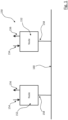
- a communication system 150 may comprise a plurality of nodes 152, each coupled to a network 160.
- Each node 152 may be configured and/or referred to as a communication device.
- the network 160 is preferably a wired network, such as an Ethernet network.
- Each node 152 may comprise a network interface 158.
- Each node 152 may send messages or receive messages via the network interface 158.
- the network interface 158 may be configured for bidirectional communication. Each message may be formed according to a predefined network protocol.
- each node 152 comprises a receive data, RXD, interface 154 and a transmit data, TXD, interface 156.
- the RXD interface 154 is used to receive data.
- the TXD interface 156 was used to send data.
- the data received via the RXD interface 154 and/or the data sent via the TXD interface 156 may comply with a (further) communication protocol.
- the nodes 152 may communicate over the network 160 by the nodes 152 exchanging messages (e.g., frames) over the network 160.
- a message to be sent over the network 160 may be formed of at least one frame.
- Each frame may comprise a series of words, each of which may be formed from a plurality of bits.
- the number of bits per word may be predefined, for example 64 bits per word.
- the frames may comply with a predefined specification, such as a network protocol, for example, an Ethernet protocol.
- a network protocol for example, an Ethernet protocol.
- frames may be exchanged between nodes 152, with each frame used for this purpose representing a timestamp.
- the timestamp of a frame may represent the time according to the internal clock of the node 152 at which the frame is sent by the node.
- nodes 152 may determine the time duration and consequently the time delay (latency) required for a frame to travel from one node 152 to another node 152.
- the nodes 152 can determine the latency to each other node 152.
- the nodes 152 can perform synchronization of internal clocks via the frames, each representing a timestamp. If many nodes 152 are coupled to a network 160 and/or if the nodes 152 are spaced apart, the latency of the frames may vary.
- the incorporation of a timestamp into a frame should be performed as close as possible to the time at which the frame is sent by a node 152. Accordingly, an internal processing time between the time the timestamp is included in the frame and the time the frame is sent by the node 152 should be very small or minimal.
- the internal processing time of a frame in a node 152 may vary considerably. For example, one frame may require encryption prior to transmission, where another frame may not require encryption prior to transmission. Without encryption, the internal processing time turns out to be shorter.
- the internal processing time of the frames in the nodes 152 may vary, such that the timestamps represented by the frames may be inaccurate in an unfavorable case and/or may not accurately represent the particular time at which a frame was sent.
- a basic idea for solving the need is based on the knowledge that the maximum, internal processing time of frames in nodes 152 can be estimated.
- the estimate of the maximum, internal processing time can be used for a buffer unit 104 within the node 152 such that a variation in the internal processing time of a frame in a node is compensated up to the maximum processing time with the effect that the varying internal processing time has no, or at most a much smaller, effect on the accuracy of synchronization of the internal clocks of multiple nodes 152 of a system 150.
- FIG. 2 schematically illustrates an example of a node 152 that comprises at least one buffer unit 104.
- the node 152 comprises an interface module 162, a timestamp module 164, a first adapter module 166, a device 100, a second adapter module 168, and a network module 170 coupled together in a series.
- the coupling forms a TXD signal path from the TXD interface 154 to the network module 170 and an RXD signal path from the network module 170 to the RXD interface 156.
- the interface module 162 may also be referred to and/or configured as a media independent interface (MII) module 162.
- MII media independent interface
- the interface module 162 may form the TXD interface 154 and the RXD interface 156.
- the timestamp module 164 may be configured to modify a frame in the TXD path so that the frame represents a timestamp.
- the timestamp may be used to synchronize the internal clocks of a plurality of nodes 152 if those plurality of nodes 152 are coupled together via the network 160.
- the first adapter module 166 may be configured to divide a frame transmitted over the TXD path 214 to the first adapter module 166 into a plurality of words. Each word comprises a predefined number of bits, such as 64 bits.
- the first adapter module 166 may further be configured to sequentially transmit the words of the frame to the device 100. In an example, the first adapter module 166 may transmit the bits of a word to the device 100 parallel in time. As a result, the first adapter module 166 may transmit the words of the frame to the device 100 one word at a time.
- the interface module 162 and/or the timestamp module 164 may each operate according to the FIFO principle.
- the FIFO principle may be performed in the interface module and/or in the timestamp module 164 at the bit level, word level, or frame level.
- the FIFO principle in the interface module 162 and/or in the timestamp module 164 may prevent temporal mixing of data from different frames in the node 152.
- the second adapter module 168 may be configured to receive sequentially words of a frame over the TXD path 214.
- the second adapter module 168 may be configured to create a data packet from received words.
- the data packet may be transmitted from the second adapter module 168 to the network module 170 via the TXD path 214.
- the network module 170 may be configured to receive the data packet via the TXD path 214. Further, the network module 170 may be configured to modify the data packet so that the data packet complies with a predefined communication protocol, for example a network protocol such as an Ethernet protocol. After modification, the network module 170 may send the modified data packet over the network interface 158.
- a predefined communication protocol for example a network protocol such as an Ethernet protocol.
- the device 100 is coupled between the first adapter module 166 and the second adapter module 168.
- the device 100 comprises a TXD input interface 172 and a TXD output interface 174.
- the device 100 may be configured to receive words of a frame via the TXD input interface 172.
- the device 100 may further be configured to transmit (other) words to the second adapter module 168 via the TXD output interface 174.
- the node 152 and/or the device 100 may be configured to process words along the RXD path 216 in a similar and/or analogous manner to how the node 152 and/or the device 100 may process words along the TXD path 214.
- Figure 3 schematically illustrates an example of a portion of the device 100 that relates to the TXD path 214.
- the device 100 may be configured in an analogous manner for the TXD path 216, even if this portion of the device 100 is not shown in Figure 3 .
- the following explanations of the example device 100 of Figure 3 may apply to a device 100 of node 152.
- the following explanations for the device 100 of Figure 3 may apply if the device 100 in a (further) example does not form part of the node 152.
- the device 100 may be a separate device 100 that can be used in another technical system or environment.
- the following explanations may apply both to an example in which the device 100 is configured as a separate device 100 and to an example in which the device 100 forms a part of the node 152.
- the device 100 comprises a data processing module 102.
- the data processing module 102 may form a physical and/or logical part of the device 100.
- the data processing module 102 may be configured to process data.
- the data processing module 102 may comprise a processing unit for processing the data. Therefore, the data processing module 102 may also be referred to and/or configured as a processor unit and/or a processor module.
- the data processing module 102 comprises an interface 106, referred to as the module input 106.
- the module input 106 may form the TXD input interface 172 of the device 100. Via the module input 106, the data processing module 102 may sequentially receive multiple words of the same frame.
- the frame may be referred to as the first frame or the first input frame.
- Each word may comprise a predefined number of bits, such as 64 bits.
- the module input 106 may comprise a data port 182 through which all bits of a (single) word are simultaneously transmittable to the module input 106 and/or the data processing module 102.
- the data port 182 may comprise a "width" corresponding to the predefined number of bits of a word.
- the data processing module 102 may receive a frame where the words of the frame are received sequentially word by word.
- the module input 106 may comprise other ports, such as the SOF port 184 and/or the EOF port 186.
- a start signal SOF1 which represents the time of an reception of a first bit of a frame at the data port 182, may be received via the SOF port 184.
- An end signal EOF 1 which represents a time of the reception of the last bit of a frame at the data port 182, may be received via the EOF port 186.
- a word received by the data processing module 102 via the module input 106 and/or the data port 182 may also be referred to as an input word.
- the data processing module 102 may be configured to process the input word and to form an output word from the processed input word.
- the output word may comprise a defined number of bits. In an example, each output word comprises the same number of bits as the input word based on which the output word was formed.
- the data processing module 102 may comprise a processing unit. In an example, the data processing module 102 may be configured to process multiple input words simultaneously. Processing an input word may comprise multiple processing steps and/or multiple processing cycles.
- the data processing module 102 comprises another interface 108, referred to as the module output 108.
- the module output 108 may be used by the data processing module 108 to sequentially send multiple output words of the same frame. Multiple output words may belong to a frame, which may also be referred to as an output frame, particularly a first output frame.
- the module output 108 may comprise a data port 218 through which all bits of a (single) output word may be sent simultaneously.
- the data port 218 may comprise a "width" corresponding to the predefined number of bits of an output word.
- the data processing module 102 may send an output frame where the output words of the output frame are sent sequentially via the data port 218.
- the module output 110 may comprise other ports, such as the SOF port 220 and/or the EOF port 222.
- a start signal SOF2 which represents the time of a transmission of a first bit of a frame at the data port 218, may be sent via the SOF port 220.
- An end signal EOF2 which represents a time of the transmission of the last bit of a frame at the data port 218, may be received via the EOF port 222.
- the device 100 comprises the buffer unit 104.
- the buffer unit 104 may form a physical and/or logical part of the device 100.
- the buffer unit 104 comprises a memory 122.
- the memory 122 may be configured to store data, such as bits of an output word.
- the buffer unit 104 may further comprise a control unit (not shown) configured to control the memory 122.
- the buffer unit 104 comprises an interface 110, also referred to as the buffer input 110.
- the module output 108 of the data processing module 102 is coupled to the buffer input 110 of the buffer unit 104.
- the buffer unit 104 may receive an output word via the buffer input 110.
- the buffer input 110 may comprise a data port 208 through which all bits of an output word may be received simultaneously.
- the data port 208 may comprise a "width" corresponding to the predefined number of bits of an output word.
- the buffer unit 104 may sequentially receive output words from the module output 108 and/or from the associated data port 218 at the buffer input 110 and/or its associated data port 208.
- the buffer input 110 may comprise other ports, such as the SOF port 224 and/or the EOF port 226.
- the start signal SOF2 may be received via the SOF port 224.
- the end signal EOF2 may be received via the EOF port 226.
- a received output word may be stored by the buffer unit 104 in the memory 122.
- the memory 122 may be configured to store the bits of an output word.
- the buffer unit 104 may be configured to store up to a fixed number of words, such as a single word only.
- the duration while an output word is stored in the memory 122 may be controlled by the buffer unit 110, in particular by the control unit of the buffer unit 110.
- the buffer unit 104 comprises another interface 114, also referred to as the input interface 114.
- the buffer unit 104 is configured to receive further data, referred to as run time data, via the input interface 114.
- the run time data represents a duration of time, referred to as run time T4, between a first time T1, at which the data processing module 102 receives an input word via the module input 106, and a second time T2, at which an output word is transmitted from the data processing module 102 via the module output 108 to the buffer input 110 of the buffer unit 104.
- the run time data preferably represents a period of time, referred to as run time T4, from the a first time T1 (in particular first point in time T1) and the second time T2 (in particular the second point in time T2).
- the output word is generated by the data processing module 102 based on the received input word.
- the run time data may represent both the first time T1 and the second time T2.
- a representation of the first and second times T1, T2 may preferably also to be understood as a representation of the duration in time between the first time T1 and the second time T2.
- the run time data may represent the first and second times T1, T2 and/or (as a result also) the run time T4.
- the data processing module 112 may comprise a through path 198.
- the data processing module 102 may be configured to process data in the through path 198 parallel in time with a received input word.
- Data may be input to the through path 198 via a path input port 228.
- a path output port 230 may be used to exit the through path 198 and transmit data.
- run time data representing the run time T4 may be transmitted to the input interface 114.
- the node 152 comprises a timestamp module 164.
- the timestamp module 164 may be configured to modify (the bits of) a frame such that the modified frame represents the timestamp generated by the timestamp module 164.
- the first word of the modified frame may represent the timestamp.
- the timestamp passes from the timestamp module 164 to the network interface 158, at which the timestamp may be represented by a (different) frame that satisfies a network protocol, such as an Ethernet protocol.
- the other frame may be referred to and/or configured as a data packet.
- a variation of the temporal duration T9 can be prevented if the temporal durations T6, T7, T8 do not vary in time, respectively.
- an adapter module 166, another adapter module 168 and a network module 170 are already available, each of which requires a constant time or a duration that does not vary in time for processing data, such as words of a frame.
- each of the temporal durations T7 and T8 do not vary in time.
- the time duration T6 may also be referred to as the reference time T6.
- the reference time T6 is shown schematically.
- the reference time T6 is the sum of the run time T4 and the delay time T5.
- the run time T4 is preferably the duration in time between the time T1 of receiving an input word by the data processing module 102 and the time T2 of transmitting an output word from the data processing module 102 to the buffer unit 104.
- the delay time T5 is preferably the duration in time between the time T2 and a time T3 at which the previously received output word is sent by the buffer unit 104.
- the maximum time duration of the run time T4 may be estimated. In an example, it may be assumed that the maximum temporal duration of the run time T4 occurs if a frame and/or its associated input words must be decrypted to generate corresponding output words. The run time T4 may be shorter if a frame's words do not need to be decrypted to generate output words. The variation of the run time T4 may be compensated by the delay time T5.
- the buffer unit 104 may also be referred to as the latency compensation unit 104. Using the run time data received by the buffer unit 104 via the input interface 114, the buffer unit 104 may determine the actual run time T4.
- the buffer unit 104 may adjust the duration while an output word is stored in the memory 122 so that the delay time T5 is short if the run time T4 is long and is long if the run time T4 is short.
- the buffer unit 104 may be configured to adjust the delay time T5 by adjusting the duration while an output word is stored in the memory 122 such that the sum of the run time T4 and the delay time T5 is preferably exactly the predefined reference time T6.
- the reference time T6 may be a constant temporal duration that is not subject to temporal variation.
- the temporal duration T9 is also constant in time as well.
- the temporal duration T9 may also be referred to as the process time T9.
- the constant process time may ensure that precise synchronization of the internal clocks of the nodes 152.
- the buffer unit 104 comprises an interface 112, referred to as the buffer output 112.
- the buffer output 112 may form the TXD output interface 174 of the device 100.
- the buffer unit 104 may send an output word (previously) stored in the memory 122 via the buffer output 112.
- the time T3 at which the buffer unit 104 sends an output word stored in the memory 122 may be controlled by the buffer unit, preferably by a control unit of the buffer unit 104.
- the buffer unit 104 may be configured to determine the time T3 depending on the run time T4 represented by the run time data.
- the buffer unit 104 may be configured to determine the time T3 depending on the run time T4 such that a sum of the delay time T5 and the run time T4 is the predefined reference time T6.
- the delay time T5 may be understood to correspond to a time duration that is predefined reference time T6 minus the running time T4.
- the predefined reference time T6 may be stored by the buffer unit 112.
- the buffer output 112 may comprise a data port 190 through which all bits of the (single) output word may be sent simultaneously.
- the data port 190 may comprise a "width "corresponding to the predefined number of bits of an output word.
- the buffer unit 104 may send an output frame where the output words of the output frame are sent sequentially via the data port 190.
- the buffer output 112 may comprise other ports, such as the first SOF port 192 and/or the EOF port 194.
- a start signal SOF3, which represents the time of a transmission of a first bit of a frame at the data port 190, may be sent via the SOF port 192.
- An end signal EOF3, which represents a time of the transmission of the last bit of a frame at the data port 190, may be received via the EOF port 194.
- the data processing module 102 is preferably configured to perform the following steps A1), A2), and A3):
- the buffer unit 104 is preferably configured to perform the following steps B1), B2), and B3):
- the run time T4 and the following delay time T5 add up to the predefined (and desired constant) reference time T6.
- the same reference time T6 is always required by the device 100 to generate and/or send an (arbitrary) first output word based on an (arbitrary) received first input word.
- a frame may be divided into a plurality of words.
- the words may be transmitted sequentially along the TXD path 214 to the device 100.
- it may be sufficient to perform step B3) for the first word of the first frame.
- All further words of the same frame follow word by word the first word along the TXD path 214, so that for all further words of the same frame have the same predefined (and desired constant) reference time T6.
- the constant reference time T6 at the device 100 can be ensured.
- the same predefined reference time T6 may be ensured for the processing of each word of a frame by the device 100.
- Such a constant, predefined reference time T6 may provide a high utilization of the network 160 and/or a high transmission speed from node 152 to node 152.
- the data processing module 102 may be configured to perform at least one of the following steps A2.1), A2.2) and A2.3) as sub-step(s) of step A2):
- the data processing module 102 may be configured to process a plurality of words of the same frame simultaneously. A plurality of words of the frame may be received sequentially by the data processing module 102 via the module input 106.
- the data processing module 102 may be configured to detect whether at least one word of the frame is encrypted based on one of the plurality of words of the frame. In an example, the data processing module 102 may detect based on the second word or third word of a frame whether any of the other words of the frame are encrypted. Provided that the data processing module 102 has detected that a word is encrypted, the data processing module 102 may perform step A2.1) in an analogous manner for the encrypted word.
- the data processing module 102 may detect that the first input word is encrypted. In this case, the data processing module 102 will perform step A2.1) in and/or as step A2). If only step A2.1) is performed in step A2), step A2.1) may replace step A2). Decrypting a word may be understood as an example for processing the word.
- the data processing module 102 may detect that the first input word is unencrypted. In this case, the data processing module 102 will perform step A2.2) in and/or as step A2). If only step A2.2) is performed in step A2), step A2.2) may replace step A2). Forwarding a word may be understood as an example for processing the word.
- the data processing module 102 may perform additional processing steps in step A2, in addition to decrypting and/or forwarding, to generate the output word based on the input word.
- step A2.3) may be performed in and/or as step A2).
- Step A2.3) may be combined with step A2.1) and/or with step A2.2).
- the data processing module 102 may be configured to, if an input word is encrypted according to the MACSec protocol, decrypt the respective input word according to the MACSec protocol such that the output word is formed by the decrypted input word.
- the corresponding decryption according to the MACSec protocol may be performed in step A2) and/or in step A2.1).
- the module output 108 of the data processing module 102 may comprise another port 124, which may also be referred to as the control input 124. Via the control input 124, the data processing module 102 may receive a signal Red2, which may also be referred to as a ready signal Red2.
- the ready signal Red2 may be generated by the buffer unit 104.
- the buffer input 110 comprises another port 126, which may be referred to as the control output 126.
- the control output 126 may be coupled to the control input 124.
- the ready signal Red2 generated by the buffer unit 104 may represent the time T3, such as by a signal change.
- the ready signal Red2 may have a predefined signal level.
- the buffer unit 104 may be configured to send the ready signal Red2 to the control input 124 of the data processing module 102 at and/or from the third time T3 via the control output 126. If the data processing module 102 receives the ready signal Red2, the data processing module 102 may sequentially transmit the other words of the first frame to the buffer input 110 of the buffer unit 104 via the module output 108.
- the ready signal Red2 can be understood approximately as meaning that, from the generation of the ready signal Red2, the (further) words of the first frame are processed word by word by the device 100. The processing of each word takes the predefined reference time T6.
- the buffer unit 104 is configured to perform the following step B4): transmit the ready signal Red2 at and/or from the third time T3 via the control input 126 to the control input 124 of the data processing module 102.
- the ready signal Red2 represents an indication to transmit at least one further word to the buffer unit 104.
- the data processing module 102 may interpret the ready signal Red2 based on the indication such that, from the time the ready signal Red2 is received, the further words of the first frame are transmitted word by word to the buffer unit 104.
- the data processing module 102 is configured to perform steps A4), A5), and A6):
- Steps A4) through A6) may be performed sequentially as a step group.
- the data processing module 102 may be configured to perform the step group for each additional input word of the frame.
- the step groups may be performed partially overlapping in time.
- step A6) is performed only while the ready signal Red2 is received, so that the ready signal Red2 can be used by the buffer unit 104 to control when further output words are transmitted to the buffer unit 104.
- the ready signal Red2 can therefore also be used to prevent further output words from being transmitted to the buffer unit 104 while the first output word is stored in the memory unit 122 during the delay time T5. Only if the first output word is sent, the further output words are transmitted word by word to the buffer unit 104.
- the output words form a closed series such that an output frame is formed from the output words.
- the step group (comprising steps A4) to A6)) may be performed parallel in time and/or overlapping in time with steps A2), and A3).
- the data processing module 102 may receive additional input words of the first frame while other input words that have already been received are processed by the data processing module 102, such as for decryption and/or for forwarding to the module output 108 for transmission to the buffer unit 104.
- the data processing module 102 may be configured to perform at least one of the following steps A5.1), A5.2), and A5.3) as sub-step(s) of step A5):
- the at least one further output word should be sent to the buffer unit 104 only if the first output word has been sent previously by the buffer unit 104 via the buffer output 112.
- the sending of the first output word is performed at time T3.
- the ready signal Red2 is sent from the buffer unit 104 to the data processing module 102.
- the data processing module 102 may be configured to prevent transmission of the at least one further output word until the ready signal Red2 is received.
- the data processing module 102 may process the input words based on the FIFO principle. The order of the words of the same frame may therefore be maintained in a process direction between the module input 106 to the buffer output 112.
- the first frame may be formed by an Ethernet frame.
- the Ethernet frame may also be referred to and/or configured as an Ethernet packet.
- the data processing module 102 may be configured to detect the first bit of a frame.
- the first bit of the frame is formed by the first bit of the first word of the first frame.
- the module input 106 may comprise a SOF port 184.
- the data processing module 102 may receive a start signal SOF1 via the SOF port 184.
- the start signal SOF1 may represent a start bit.
- the start bit is transmitted by the start signal SOF1 to the data processing module 102 at the time T 1.
- the data processing module 102 may be configured to receive both the start bit represented by the start signal SOF1 and the first bit of the first input word in parallel in time via the module input 106.
- the data processing module 102 may further be configured to detect the time T1 by a sensing of the time of reception of the start bit based on the start signal SOF1. In other words, the time T1 may be detected particularly easily based on the start signal SOF 1.
- the buffer unit 104 may receive the run time data via the input interface 114 of the buffer unit 104.
- the run time data may represent both the first time period T1 and the second time period T2.
- the first time period T1 refers to the reception of the first input word by the data processing module 102.
- the second time period refers to the transmission of the first output word from the data processing module 102 to the buffer unit 104.
- the buffer unit 104 may be configured to calculate the run time T4 based on the first and the second times T1, T2. Once the run time T4 is calculated, the buffer unit 104 may subtract the run time T4 from the reference time T6 to determine the remaining delay time T5. The buffer unit 104 may be configured to buffer (only) the first output word for exactly the delay time T5. Subsequent output words of the same frame may be forwarded by the buffer unit 104 without applying the delay time T5.
- the run time data may be divided into two parts.
- the run time data may be formed of a first data part and a second data part.
- the buffer unit 104 may be configured to receive the two data parts separately via the input interface 114.
- the first data part may represent the first time T1.
- the second data part may represent the second time T2.
- the two data parts may come from different sources.
- a first sensor may be used for the device 100 to detect the first time T1.
- the first sensor may detect the time of receiving the first input word and/or the time of receiving the start bit (represented by the SOF1 signal).
- the device 100 may comprise another sensor to detect the time of transmission of the first output word from the data processing module 102 to the buffer unit 104.
- the first sensor may generate and transmit the first data part to the input interface 114.
- the second sensor may generate and transmit the second data part to the input interface 114.
- the two sensors may be coupled to each other.
- the two sensors may be configured to transmit the two data parts to the input interface 114 of the buffer unit 104 in parallel in time.
- the buffer unit 104 may be configured to receive the first data part and the second data part in parallel in time.
- the data processing module 102 may be configured to generate the first data part representing the first time T1.
- the input interface 114 of the buffer unit 104 may be coupled to the module output 108 of the data processing module 102.
- the data processing module 102 may further be configured to transmit the first data part to the input interface 114 of the buffer unit 104.
- the device 100 may comprise a counter unit 136, such as a free counter.
- the input interface 114 of the buffer unit 104 may be coupled to the counter unit 136.
- the counter unit 136 may be configured to generate the second data part representing the second time T2.
- the counter unit 136 may transmit the second data part to the input interface 114 of the buffer unit 104.
- the counter unit 136 is configured to periodically generate timestamps. For each generated timestamp, the counter unit 136 may generate a second data part representing the respective timestamp and transmit the second data part to the input interface 114 of the buffer unit 104. Second data parts may be periodically transmitted from the counter unit 136 to the input interface 114 of the buffer unit 104.
- the buffer unit 104 may be configured to solely accept, select, and/or receive the second data part that is received in parallel time with the first data part.
- the corresponding, second data part represents the time T2 at which the first output word is transmitted from the data processing module 102 to the buffer unit 104.
- the counter unit 136 may be coupled to the module input 106 of the data processing module 102.
- the data processing module 102 may be configured to generate a third data part representing the respective timestamp for each generated timestamp.
- the counter unit 136 may transmit each third data part to the module input 106.
- the counter unit 136 transmits each third data part to the path input port 228 of the module input 106.
- the data processing module 102 is configured to process the third data part received at the path input port 228 in parallel time with the first input word at the data port 182.
- the third data part received by the data processing module 102 in parallel in time with the first input word may be referred to as the first data part.
- the data processing module 102 may process the first data part in parallel in time with the step A2). In the step A2, the data processing module generates the first output word based on the first input word.
- the data processing module 102 may further be configured to transmit the first data part and the first output word to the buffer unit 104 in parallel in time.
- the data processing module 102 may comprise the through path 198 that forms a processing path from the path input port 228 of the module input 106 to the path output port 230 of the module output 108.
- the data processing module 102 may transmit the first data part from the path output port 230 to the input interface 114 of the buffer unit 104.
- the first data part represents the time T1 at which the data processing module 102 received the first input word via the module input 106.
- Transmission of the first data part to the input interface 114 of the buffer unit 104 also simultaneously sets the time at which the buffer unit 104 accepts and/or selects a second data part to be transmitted from the counter unit 136 to the input interface 114 of the buffer unit 104.
- the selected and/or accepted second data part represents the time at which the first output word is transmitted from the data processing module 102 to the buffer unit 104.
- the input interface 114 of the buffer unit 104 receives both the first data part and the second data part in parallel in time.
- the buffer unit receives information about the first time T1 and the second time T2. From the two times T1, T2, the buffer unit can determine the run time T4.
- the reference time T6 is predefined and may be stored by the buffer unit 104.
- the buffer unit 104 can determine the delay time T5 from the reference time T6 and the processing time T4.
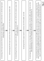
- the device 100 comprising a data processing module 102, and a buffer unit 104, wherein the data processing module 102 comprises a module input 106, and a module output 108, wherein the buffer unit 104 comprising a buffer input 110, a buffer output 112, and an input interface 114, wherein the module output 108 is coupled to the buffer input 110, and wherein the method comprising the steps:
- the systems and methods described herein may at least partially be embodied by a computer program or a plurality of computer programs, which may exist in a variety of forms both active and inactive in a single computer system or across multiple computer systems.
- they may exist as software program(s) comprised of program instructions in source code, object code, executable code or other formats for performing some of the steps.
- Any of the above may be embodied on a computer-readable medium, which may include storage devices and signals, in compressed or uncompressed form.
- the term "computer” refers to any electronic device comprising a processor, such as a general-purpose central processing unit (CPU), a specific-purpose processor or a microcontroller.
- a computer is capable of receiving data (an input), of performing a sequence of predetermined operations thereupon, and of producing thereby a result in the form of information or signals (an output).
- the term "computer” will mean either a processor in particular or more generally a processor in association with an assemblage of interrelated elements contained within a single case or housing.
- processor or “processing unit” refers to a data processing circuit that may be a microprocessor, a co-processor, a microcontroller, a microcomputer, a central processing unit, a field programmable gate array (FPGA), a programmable logic circuit, and/or any circuit that manipulates signals (analog or digital) based on operational instructions that are stored in a memory.
- memory refers to a storage circuit or multiple storage circuits such as read-only memory, random access memory, volatile memory, non-volatile memory, static memory, dynamic memory, Flash memory, cache memory, and/or any circuit that stores digital information.
- a "computer-readable medium” or “storage medium” may be any means that can contain, store, communicate, propagate, or transport a computer program for use by or in connection with the instruction execution system, apparatus, or device.
- the computer-readable medium may be, for example but not limited to, an electronic, magnetic, optical, electromagnetic, infrared, or semiconductor system, apparatus, device, or propagation medium.
- the computer-readable medium may include the following: an electrical connection having one or more wires, a portable computer diskette, a random-access memory (RAM), a read-only memory (ROM), an erasable programmable read-only memory (EPROM or Flash memory), an optical fiber, a portable compact disc read-only memory (CDROM), a digital versatile disc (DVD), a Blu-ray disc (BD), and a memory card.
- RAM random-access memory
- ROM read-only memory
- EPROM or Flash memory erasable programmable read-only memory
- CDROM compact disc read-only memory
- DVD digital versatile disc
- BD Blu-ray disc
Landscapes
- Engineering & Computer Science (AREA)
- Computer Security & Cryptography (AREA)
- Signal Processing (AREA)
- Computer Networks & Wireless Communication (AREA)
- Computer Hardware Design (AREA)
- General Engineering & Computer Science (AREA)
- Theoretical Computer Science (AREA)
- Computing Systems (AREA)
- Health & Medical Sciences (AREA)
- Software Systems (AREA)
- Physics & Mathematics (AREA)
- General Physics & Mathematics (AREA)
- General Health & Medical Sciences (AREA)
- Bioethics (AREA)
- Multimedia (AREA)
- Data Exchanges In Wide-Area Networks (AREA)
- Communication Control (AREA)
Priority Applications (3)
| Application Number | Priority Date | Filing Date | Title |
|---|---|---|---|
| EP23170592.2A EP4456512A1 (de) | 2023-04-28 | 2023-04-28 | Vorrichtung und verfahren für die vorrichtung |
| CN202410394078.XA CN118866032A (zh) | 2023-04-28 | 2024-04-02 | 装置和用于所述装置的方法 |
| US18/639,724 US20240364664A1 (en) | 2023-04-28 | 2024-04-18 | Device and a method for the device |
Applications Claiming Priority (1)
| Application Number | Priority Date | Filing Date | Title |
|---|---|---|---|
| EP23170592.2A EP4456512A1 (de) | 2023-04-28 | 2023-04-28 | Vorrichtung und verfahren für die vorrichtung |
Publications (1)
| Publication Number | Publication Date |
|---|---|
| EP4456512A1 true EP4456512A1 (de) | 2024-10-30 |
Family
ID=86282592
Family Applications (1)
| Application Number | Title | Priority Date | Filing Date |
|---|---|---|---|
| EP23170592.2A Pending EP4456512A1 (de) | 2023-04-28 | 2023-04-28 | Vorrichtung und verfahren für die vorrichtung |
Country Status (3)
| Country | Link |
|---|---|
| US (1) | US20240364664A1 (de) |
| EP (1) | EP4456512A1 (de) |
| CN (1) | CN118866032A (de) |
Citations (2)
| Publication number | Priority date | Publication date | Assignee | Title |
|---|---|---|---|---|
| EP3840255A1 (de) * | 2019-12-20 | 2021-06-23 | Juniper Networks, Inc. | Zeitsynchronisation für verschlüsselten verkehr in einem computernetzwerk |
| US20220116373A1 (en) * | 2021-12-22 | 2022-04-14 | Choon Yip Soo | Systems and methods for communicating encrypted time-related data |
Family Cites Families (7)
| Publication number | Priority date | Publication date | Assignee | Title |
|---|---|---|---|---|
| EP1238489B1 (de) * | 1999-12-13 | 2008-03-05 | Broadcom Corporation | Sprach-durchgangsvorrichtung mit sprachsynchronisierung in abwärtsrichtung |
| US20070174429A1 (en) * | 2006-01-24 | 2007-07-26 | Citrix Systems, Inc. | Methods and servers for establishing a connection between a client system and a virtual machine hosting a requested computing environment |
| US20130212334A1 (en) * | 2012-02-09 | 2013-08-15 | Qualcomm Incorporated | Determining Optimal Preload Distance at Runtime |
| US9690555B2 (en) * | 2015-06-29 | 2017-06-27 | International Business Machines Corporation | Optimization of application workflow in mobile embedded devices |
| US10043021B2 (en) * | 2016-04-07 | 2018-08-07 | Blackberry Limited | Controlling access to application data |
| US10931391B2 (en) * | 2017-09-27 | 2021-02-23 | Intel Corporation | One-step time stamping of synchronization packets for networked devices |
| CN111758045B (zh) * | 2018-01-03 | 2024-07-09 | 混合雷达系统公司 | 用于测量两个事件之间信号传输时间的装置和方法 |
-
2023
- 2023-04-28 EP EP23170592.2A patent/EP4456512A1/de active Pending
-
2024
- 2024-04-02 CN CN202410394078.XA patent/CN118866032A/zh active Pending
- 2024-04-18 US US18/639,724 patent/US20240364664A1/en active Pending
Patent Citations (2)
| Publication number | Priority date | Publication date | Assignee | Title |
|---|---|---|---|---|
| EP3840255A1 (de) * | 2019-12-20 | 2021-06-23 | Juniper Networks, Inc. | Zeitsynchronisation für verschlüsselten verkehr in einem computernetzwerk |
| US20220116373A1 (en) * | 2021-12-22 | 2022-04-14 | Choon Yip Soo | Systems and methods for communicating encrypted time-related data |
Also Published As
| Publication number | Publication date |
|---|---|
| US20240364664A1 (en) | 2024-10-31 |
| CN118866032A (zh) | 2024-10-29 |
Similar Documents
| Publication | Publication Date | Title |
|---|---|---|
| US11689440B2 (en) | Method and apparatus for transmit time timestamping | |
| KR101610270B1 (ko) | 네트워크 요소들에서 정밀 시간 프로토콜 및 미디어 액세스 제어 보안을 통합하기 위한 방법 및 장치 | |
| US11277455B2 (en) | Streaming system | |
| US10931391B2 (en) | One-step time stamping of synchronization packets for networked devices | |
| CN104012025B (zh) | 时戳及mac安全性的物理层处理 | |
| US9602271B2 (en) | Sub-nanosecond distributed clock synchronization using alignment marker in ethernet IEEE 1588 protocol | |
| US8325616B2 (en) | Method and system for determination and exchange of network timing information | |
| US9042411B1 (en) | System and method for accurate time sampling in presence of output delay | |
| CN107666384B (zh) | 更新加密密钥的方法和设备 | |
| JP6222802B2 (ja) | ランダム値生成方法およびシステム | |
| EP4203382A1 (de) | Systeme und verfahren zur kommunikation verschlüsselter zeitbezogener daten | |
| WO2021022794A1 (zh) | 基于rdma的数据传输方法、网卡、服务器及介质 | |
| US10599587B2 (en) | High latency channel and low latency channel | |
| KR20170105573A (ko) | Otn 네트워크에서의 시간 동기화 방법, 기기, 시스템 및 저장 매체 | |
| JP6743898B2 (ja) | 通信装置、通信方法、通信システム及び通信プログラム | |
| US20210266205A1 (en) | Modulating signal level transitions to increase data throughput over communication channels | |
| Eckhardt et al. | Analysis of the round trip time of opc ua and tsn based peer-to-peer communication | |
| EP4456512A1 (de) | Vorrichtung und verfahren für die vorrichtung | |
| CN109617676B (zh) | 一种密码同步方法、通信节点、电子设备和可读存储介质 | |
| CN116261000A (zh) | 一种云会议中音视频的同步方法、装置和电子设备 | |
| US20240364611A1 (en) | Module for a communication device, a corresponding communication device, and a method for the module | |
| CN108777601B (zh) | 一种时钟同步方法、装置及网络设备 | |
| KR102937891B1 (ko) | 시간 민감형 네트워킹을 위한 데이터 암호화 방법, 데이터 암호화 장치 및 기록 매체에 저장된 프로그램 | |
| US20250220004A1 (en) | Accurate Timestamp Measurements for a Single Step Precision Time Protocol | |
| CN112350920A (zh) | 基于区块链的即时通讯系统 |
Legal Events
| Date | Code | Title | Description |
|---|---|---|---|
| PUAI | Public reference made under article 153(3) epc to a published international application that has entered the european phase |
Free format text: ORIGINAL CODE: 0009012 |
|
| STAA | Information on the status of an ep patent application or granted ep patent |
Free format text: STATUS: THE APPLICATION HAS BEEN PUBLISHED |
|
| AK | Designated contracting states |
Kind code of ref document: A1 Designated state(s): AL AT BE BG CH CY CZ DE DK EE ES FI FR GB GR HR HU IE IS IT LI LT LU LV MC ME MK MT NL NO PL PT RO RS SE SI SK SM TR |
|
| STAA | Information on the status of an ep patent application or granted ep patent |
Free format text: STATUS: REQUEST FOR EXAMINATION WAS MADE |
|
| 17P | Request for examination filed |
Effective date: 20250430 |
|
| GRAP | Despatch of communication of intention to grant a patent |
Free format text: ORIGINAL CODE: EPIDOSNIGR1 |
|
| STAA | Information on the status of an ep patent application or granted ep patent |
Free format text: STATUS: GRANT OF PATENT IS INTENDED |
|
| INTG | Intention to grant announced |
Effective date: 20260102 |
|
| GRAJ | Information related to disapproval of communication of intention to grant by the applicant or resumption of examination proceedings by the epo deleted |
Free format text: ORIGINAL CODE: EPIDOSDIGR1 |
|
| STAA | Information on the status of an ep patent application or granted ep patent |
Free format text: STATUS: REQUEST FOR EXAMINATION WAS MADE |
|
| INTC | Intention to grant announced (deleted) | ||
| GRAP | Despatch of communication of intention to grant a patent |
Free format text: ORIGINAL CODE: EPIDOSNIGR1 |
|
| STAA | Information on the status of an ep patent application or granted ep patent |
Free format text: STATUS: GRANT OF PATENT IS INTENDED |