EP4456358A1 - Protection in a direct current high voltage electric system - Google Patents
Protection in a direct current high voltage electric system Download PDFInfo
- Publication number
- EP4456358A1 EP4456358A1 EP23170425.5A EP23170425A EP4456358A1 EP 4456358 A1 EP4456358 A1 EP 4456358A1 EP 23170425 A EP23170425 A EP 23170425A EP 4456358 A1 EP4456358 A1 EP 4456358A1
- Authority
- EP
- European Patent Office
- Prior art keywords
- connection
- coupling
- resistor
- supply
- output terminal
- Prior art date
- Legal status (The legal status is an assumption and is not a legal conclusion. Google has not performed a legal analysis and makes no representation as to the accuracy of the status listed.)
- Pending
Links
Images



Classifications
-
- H—ELECTRICITY
- H02—GENERATION; CONVERSION OR DISTRIBUTION OF ELECTRIC POWER
- H02H—EMERGENCY PROTECTIVE CIRCUIT ARRANGEMENTS
- H02H3/00—Emergency protective circuit arrangements for automatic disconnection directly responsive to an undesired change from normal electric working condition with or without subsequent reconnection ; integrated protection
- H02H3/08—Emergency protective circuit arrangements for automatic disconnection directly responsive to an undesired change from normal electric working condition with or without subsequent reconnection ; integrated protection responsive to excess current
- H02H3/087—Emergency protective circuit arrangements for automatic disconnection directly responsive to an undesired change from normal electric working condition with or without subsequent reconnection ; integrated protection responsive to excess current for DC applications
-
- H—ELECTRICITY
- H02—GENERATION; CONVERSION OR DISTRIBUTION OF ELECTRIC POWER
- H02H—EMERGENCY PROTECTIVE CIRCUIT ARRANGEMENTS
- H02H3/00—Emergency protective circuit arrangements for automatic disconnection directly responsive to an undesired change from normal electric working condition with or without subsequent reconnection ; integrated protection
- H02H3/08—Emergency protective circuit arrangements for automatic disconnection directly responsive to an undesired change from normal electric working condition with or without subsequent reconnection ; integrated protection responsive to excess current
- H02H3/10—Emergency protective circuit arrangements for automatic disconnection directly responsive to an undesired change from normal electric working condition with or without subsequent reconnection ; integrated protection responsive to excess current additionally responsive to some other abnormal electrical conditions
-
- H—ELECTRICITY
- H02—GENERATION; CONVERSION OR DISTRIBUTION OF ELECTRIC POWER
- H02H—EMERGENCY PROTECTIVE CIRCUIT ARRANGEMENTS
- H02H9/00—Emergency protective circuit arrangements for limiting excess current or voltage without disconnection
- H02H9/04—Emergency protective circuit arrangements for limiting excess current or voltage without disconnection responsive to excess voltage
- H02H9/042—Emergency protective circuit arrangements for limiting excess current or voltage without disconnection responsive to excess voltage comprising means to limit the absorbed power or indicate damaged over-voltage protection device
-
- B—PERFORMING OPERATIONS; TRANSPORTING
- B64—AIRCRAFT; AVIATION; COSMONAUTICS
- B64D—EQUIPMENT FOR FITTING IN OR TO AIRCRAFT; FLIGHT SUITS; PARACHUTES; ARRANGEMENT OR MOUNTING OF POWER PLANTS OR PROPULSION TRANSMISSIONS IN AIRCRAFT
- B64D45/00—Aircraft indicators or protectors not otherwise provided for
-
- H—ELECTRICITY
- H02—GENERATION; CONVERSION OR DISTRIBUTION OF ELECTRIC POWER
- H02H—EMERGENCY PROTECTIVE CIRCUIT ARRANGEMENTS
- H02H7/00—Emergency protective circuit arrangements specially adapted for specific types of electric machines or apparatus or for sectionalised protection of cable or line systems, and effecting automatic switching in the event of an undesired change from normal working conditions
- H02H7/008—Emergency protective circuit arrangements specially adapted for specific types of electric machines or apparatus or for sectionalised protection of cable or line systems, and effecting automatic switching in the event of an undesired change from normal working conditions for protective arrangements according to this subclass
-
- H—ELECTRICITY
- H03—ELECTRONIC CIRCUITRY
- H03K—PULSE TECHNIQUE
- H03K17/00—Electronic switching or gating, i.e. not by contact-making and –breaking
- H03K17/08—Modifications for protecting switching circuit against overcurrent or overvoltage
- H03K17/081—Modifications for protecting switching circuit against overcurrent or overvoltage without feedback from the output circuit to the control circuit
- H03K17/0814—Modifications for protecting switching circuit against overcurrent or overvoltage without feedback from the output circuit to the control circuit by measures taken in the output circuit
Definitions
- the present invention relates to an electrical arrangement for protection in a direct current high voltage electric system, to an electric system with a direct current network, to an aircraft and to a method for protected switching in a direct current high voltage electric system.
- switching components can be provided, such as for deactivating the system to avoid unwanted conditions.
- An example are switches or fuses that provide a temporal disconnection.
- additional measures like clamping circuits, need to be provided to avoid a temporal overload situation due to the switching-off.
- clamping devices like varistors and Zener diodes require a complex matching procedure and may result in rather bulky arrangements.
- an electrical arrangement for protection in a direct current high voltage electric system comprises an input connection with an input terminal, an output connection with an output terminal, a main disconnection component between the input terminal and the output terminal and at least one clamping circuit between the input terminal and the output terminal.
- the clamping circuit has a first connecting path and a second connecting path, arranged in parallel to each other.
- the first connection path comprises a storage coupling for temporarily buffering an overvoltage present between the input terminal and the output terminal and an activatable switch for selectably connecting the storage coupling with the output terminal.
- the second connection path comprises a supply coupling for operating the activatable switch in dependency of the overvoltage.
- the main switching element can thus be provided in a more efficient and targeted manner.
- the energy stored on the lines e.g. due to inductance, can be absorbed by the clamping circuit.
- the clamping circuit is arranged in parallel to a main switch or fuse.
- the main disconnection component is a safety element configured to open an electrical circuit in the direct current high voltage electric system in order to protect at least a part of the electrical circuit.
- the storage coupling comprises a capacitor and a first resistor in a parallel connection.
- the storage coupling also comprises a second resistor in series with the parallel connection of the capacitor and the first resistor.
- the activatable switch comprises a semiconductor switch that is blocked in a first state and that provides a connection to the output terminal in a second state.
- the activatable switch comprises an enhancement type field-effect-transistor, which is connected to the storage coupling with its drain connector, to the output terminal with its source connector and to the supply coupling with its gate as control coupling.
- the supply coupling comprises a first coupling resistor and a second coupling resistor connected in series between the input terminal and the output terminal.
- a trigger element is provided that comprises an input voltage terminal connected to a connection point between the first coupling resistor and the second coupling resistor with its positive connector and to a reference voltage connection with its negative connector.
- the trigger element also comprises a supply voltage terminal connected to a supply source with its positive connector and to output terminal with its negative connector.
- the trigger element is configured to provide a switch supply voltage to the gate of the activatable switch in order to close the activatable switch for activating the storage coupling.
- the supply coupling comprises a first transorber, a second transorber and a third transorber connected in series.
- a supply resistor is connected to a connection point of the second transorber and the third transorber, and a supply diode connected between the supply resistor and the activatable switch.
- the diode is connected to the supply resistor with its anode end.
- a supply filter capacitor is connected between a connection point of the supply resistor and the supply diode.
- a pull down resistor is connected between the gate and the output terminal.
- An overvoltage protection diode is connected between the gate and the output terminal.
- the electrical arrangement is provided as a bi-directional electrical arrangement.
- the input connection comprises a first input terminal and a second input terminal.
- the main disconnection component comprises a first main disconnection element between the first input terminal and the output terminal, and a second main disconnection element between the second input terminal and the output terminal.
- the clamping circuit is provided as a first clamping circuit between the first input terminal and a midpoint terminal, and a second clamping circuit is provided between the second input terminal and the midpoint terminal.
- the first clamping circuit has the first connecting path and the second connecting path; and the second clamping circuit has a third connecting path and a fourth connecting path, arranged in parallel to each other.
- the third connection path comprises a second storage coupling for temporarily buffering an overvoltage present between the second input terminal and the midpoint terminal, and a second activatable switch for selectably connecting the second storage coupling with the output terminal.
- the fourth connection path comprises a second supply coupling for operating the second activatable switch in dependency of the overvoltage.
- the second connection path and the fourth connection path are provided at least partly as a shared connection path.
- an electric system with a direct current network comprises at least one source, at least one load and an electrical arrangement according to one of the preceding examples.
- the source is selected from the group of: batteries, super capacitors, fuel cells, solar cells, power network and combinations thereof.
- the at least one load comprises at least one of the group of: electrical engines, electric drives and motors, electric actuators.
- the source is connected to the at least one load via an electric connection.
- the electrical arrangement is provided within the electric connection such that the main disconnection component can temporarily disconnect the least one load from the source.
- the direct current network is provided on board of a vehicle comprising at least one of the group of an aircraft and an automotive.
- the electrical arrangement is configured to handle voltages larger than 800 V and currents larger than 1000 A.
- an aircraft comprising a fuselage structure comprising a use portion, a lift and propulsion structure connected to the fuselage structure and an electric system with a direct current network according to one of the preceding examples.
- the electric system is configured to be at least temporarily used for an operation of the aircraft.
- a method for protected switching in a direct current high voltage electric system comprises the steps of: providing an electrical arrangement for protection according to one of the preceding examples in the direct current high voltage electric system; and activating the main disconnection component.
- the clamping circuit is temporarily absorbing at least a part of an excess energy present as an overcurrent in the direct current high voltage electric system at the time of activating the main disconnection component.
- a component for disconnection in a high voltage circuit is supplemented with a topology that provides a buffer for temporarily storing energy that is still present when the disconnection of the circuit takes place by the component for disconnection.
- the topology also provides the possibility for draining the buffer automatically.
- Fig. 1 schematically shows an example of an electrical arrangement 10 for protection in a direct current high voltage electric system.
- the arrangement 10 comprises an input connection 12 with an input terminal 14.
- the arrangement 10 also comprises an output connection 16 with an output terminal 18.
- the arrangement 10 further comprises a main disconnection component 20 between the input terminal and the output terminal and at least one clamping circuit 22 between the input terminal 14 and the output terminal 18.
- the clamping circuit 22 has a first connecting path 24 and a second connecting path 26, arranged in parallel to each other.
- the first connection path 24 comprises a storage coupling 28 for temporarily buffering an overvoltage present between the input terminal 14 and the output terminal 18.
- the first connection path 24 also comprises an activatable switch 30 for selectably connecting the storage coupling 28 with the output terminal.
- the second connection path 26 comprises a supply coupling 32 for operating the activatable switch in dependency of the overvoltage.
- the at least one clamping circuit 22 between the input terminal 14 and the output terminal 18 is connected in parallel to the main disconnection component.
- the main disconnection component 20 provides a conducting state as a normal state. Only if a predetermined maximum current level is exceeded, the main disconnection component turns into a high-resistance state.
- the main disconnection component 20 can also be referred to as main disconnector, main switch, main switchable component or main switching component.
- the main disconnection component 20 acts like an electronic fuse.
- the input terminal 14 is a positive input terminal and the output terminal 18 is a negative output terminal.
- the clamping circuit 22 provides a controlled clamping circuit.
- the clamping circuit 22 provides the effect of absorbing an energy stored within the network or circuit when interrupting an electric current in the circuit.
- the conductors provide an inductivity that results in urging to continue a current when suddenly interrupted.
- the clamping circuit 22 provides a limitation or clamping of voltage when opening the circuit.
- the main disconnection component 20 is provided as a safety element configured to open an electrical circuit in the direct current high voltage electric system in order to protect at least a part of the electrical circuit.
- the main disconnection component 20 is provided as a fuse that opens the connection when exceeding a predetermined threshold current.
- the main disconnection component 20 is a fuse within a positive conductor of a system circuit.
- the system circuit relates to an avionic system of an aircraft.
- the storage coupling 28 is used to charge the capacitor when an overvoltage between the input terminal 14 and the output terminal 18 is detected.
- the activatable switch 30 for selectably connecting the storage coupling with the output terminal is configured to activate the clamping circuit in case of an overcurrent.
- Fig. 2 shows an example of an electric system 100 with a direct current network.
- the electric system 100 comprises at least one source 102 and at least one load 104.
- the electric system 100 further comprises an example of the electrical arrangement 10 according to one of the examples above and below.
- the source 102 is selected from the group of: batteries, super capacitors, fuel cells, solar cells, power network and combinations thereof.
- the at least one load 104 comprises at least one of the group of: electrical engines, electric drives and motors, electric actuators.
- the source 102 is connected to the at least one load 104 via an electric connection 106.
- the electrical arrangement 10 is provided within the electric connection 106 such that the main disconnection component can temporarily disconnect the least one load 104 from the source 102.
- the electric system 100 comprises multiple sources 102.
- the direct current network is provided on board of a vehicle, such as an aircraft or an automotive.
- the electrical arrangement is configured to handle voltages larger than 800 V and currents larger than 1000 A.
- Fig. 3 shows an example of an aircraft 150.
- the aircraft 150 comprises a fuselage structure 152 comprising a use portion.
- the aircraft 150 further comprises a lift and propulsion structure 154 connected to the fuselage structure 152.
- the aircraft 150 also comprises an example of the electric system 100 with a direct current network according to one of the examples above and below.
- the electric system 100 is configured to be at least temporarily used for an operation of the aircraft 150.
- the electric system 100 is used for the propulsion or for adjusting flight components.
- the use portion is a cabin area 156 or a cargo area within the fuselage.
- the lift and propulsion structure 154 may comprise, among others, a pair of wings 158 and engines 160 mounted to the wings.
- Fig. 4 shows basic steps of an example of a method 200 for protected switching in a direct current high voltage electric system.
- the method 200 comprises the following steps: In a first step 202, an electrical arrangement for protection according to one of the examples above and below are provided in the direct current high voltage electric system. In a second step 204, the main disconnection component is activated, and the clamping circuit is temporarily absorbing at least a part of an excess energy present as an overcurrent in the direct current high voltage electric system at the time of activating the main disconnection component.
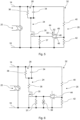
- Fig. 5 shows an example of a configuration of the electrical arrangement 10 of Fig. 1 .
- the storage coupling 28 of the first connecting path 24 comprises a capacitor 34 and a first resistor 36 in a parallel connection.
- the storage coupling 28 also comprises a second resistor 38 in series with the parallel connection of the capacitor 34 and the first resistor 36.
- the capacitor 34 is constantly discharged via the first resistor 36.
- the capacitor 34 is connected to the input terminal 14 on the one side and to the activatable switch 30 on the other side.
- the first resistor 36 can also be referred to as discharge resistor.
- the second resistor 38 is provided as an additional option in combination with the first resistor 36 and the capacitor 34.
- the second resistor 38 is coupled between the parallel connection and the activatable switch 30.
- the second resistor 38 restricts the current flow and also absorbs energy.
- the capacitor 34 is provided in a non-charged state.
- the main disconnection component 20 is provided as a semiconductor switch that provides a connection in a first state and that is blocked in a second state when exceeding a predetermined threshold current.
- the semiconductor switch is bridged by a diode element connected to the input terminal with its cathode.
- the activatable switch 30 comprises a semiconductor switch that is blocked in a first state and that provides a connection to the output terminal in a second state.
- the activatable switch 30 comprises an enhancement type field-effect-transistor, which is connected to the storage coupling 28 with its drain connector, to the output terminal 18 with its source connector and to the supply coupling 32 with its gate.
- the switch In a normal state, the switch is open, and the capacitor does not get loaded or charged.
- a pull down resistor 37 is connected between the gate and the output terminal 18.
- an overvoltage protection diode 39 is connected between the gate and the output terminal 18.
- the overvoltage protection diode 39 can also be referred to as transorber, with the same reference numeral 39.
- the resistor 37 is a pull-down resistor to keep the activatable switch 30 closed.
- the pull-down resistor 37 pulls the gate to zero, such that the transistor is turned off, in case that there is no supply, which avoids unwanted charge of the gate capacitance.
- the transorber 39 is provided as a gate protection.
- the transorber 39 is also referred to as transient voltage suppression diode.
- the transorber 39 is provided as additional option to the pull down resistor 37.
- the first resistor 36 with the capacitor 34 in parallel connection are provided connected to the activatable switch 30.
- the first and second coupling resistors 40, 42 are provided together with the trigger element 44 as well as the pull down resistor 37.
- Fig. 6 shows another example of a configuration of the electrical arrangement 10 of Fig. 1 .
- the supply coupling 32 comprises a first coupling resistor 40 and a second coupling resistor 42 connected in series between the input terminal 14 and the output terminal 18.
- a trigger element 44 is provided that comprises an input voltage terminal 46 connected to a connection point between the first coupling resistor 40 and the second coupling resistor 42 with its positive connector, and to a reference voltage connection 48 with its negative connector 49.
- the reference voltage connection 48 is also referred to as V ref .
- the trigger element 44 comprises a supply voltage terminal 50 connected to a supply source 52 with its positive connector and to the output terminal 18 with its negative connector.
- the supply source 52 is also referred to as V supply .
- the trigger element 44 is configured to provide a switch supply voltage to the gate of the activatable switch 30 in order to close the activatable switch 30 for activating the storage coupling 28.
- the first and second coupling resistor 40, 42 provide a dividing of the voltage in half design, to fit the needs of the control circuit to switch at the desired voltage.
- the first resistor 36 with the capacitor 34 in parallel connection are provided together with the second resistor 38 in series connection connected to the activatable switch 30.
- the first and second coupling resistors 40, 42 are provided together with the trigger element 44 as well as the transorber and the pull down resistor.
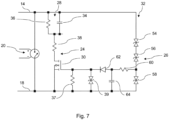
- Fig. 7 shows a further example of a configuration of the electrical arrangement 10 of Fig. 1 .
- the supply coupling 32 comprises a first transorber 54, a second transorber 56 and a third transorber 58 connected in series.
- a supply resistor 60 is connected to a connection point of the second transorber 56 and the third transorber 58, and a supply diode 62 is connected between the supply resistor 60 and the activatable switch 30.
- the supply diode 62 is connected to the supply resistor 60 with its anode end.
- a supply filter capacitor 64 is connected between a connection point of the supply resistor 60 and the supply diode 62.
- the supply filter capacitor 64 acts as a low pass filter together with the supply resistor 60.
- the supply resistor 60, the supply diode 62 and the supply filter capacitor 64 are referencing to the transorber setup.
- an external supply voltage is not needed for activating, i.e. operating the activatable switch.
- the first, second and third transorbers 54, 56, 58 provide a voltage dependent series connection.
- the first and second transorbers 54, 56 may be provided as higher-voltage transorbers.
- the third transorber 58 is configured for a lower gate voltage for the activatable switch 30.
- the pull down resistor 37 and the transorber 39 are provided in combination with the first coupling resistor 40 and the second coupling resistor 40 connected in series and the trigger element 44.
- the pull down resistor 37 and the transorber 39 are provided in combination with the first transorber 54, the second transorber 56 and the third transorber 58 connected in series, as well as the supply resistor 60 and the supply diode 62 and the supply filter capacitor 64.
- the first resistor 36 with the capacitor 34 in parallel connection are provided together with the second resistor 38 in series connection connected to the activatable switch 30.
- the first transorber 54, the second transorber 56 and the third transorber 58 are provided together with the supply resistor 60, the supply diode 62 and the supply filter capacitor 64 as well as the transorber 39 and the pull down resistor 37.
- the electrical arrangement is provided as a uni-directional electrical arrangement comprising the main disconnection component.
- the electrical arrangement is provided for a use in the field of power electronics to solve problems during switching, such as opening of a fuse or a safety switch, in high power DC networks.
- the electrical arrangement provides high performance overvoltage clamping and ensures a proper operation of such networks in case of a failure where the safety element, e.g. fuse, is triggered.
- the electrical arrangement provides a controlled electronic solution to overcome existing problems.
- Fig. 7 also comes with a redundancy feature and does not require an auxiliary voltage supply. Also the energy distribution and switch protection during switching or fuse blow is considered.
- a solution for clamping overvoltages generated when a DC network is opened, e.g. a fuse, in case of failure.
- the active current or even worse, failure current, comes with a high amount of stored energy in the unavoidable parasitic inductances of the cables/network.
- the safety element triggers and opens the circuit, this energy is absorbed to avoid very high overvoltage.
- protection is provided.
- the electrical arrangement provides improved flexibility and enhanced performance. Further, redundancy concepts can be combined with reasonable weight compared to actual solutions.
- the electrical arrangement benefits from a combination of a fast and controllable energy storage and clamping method based on a fast semiconductor switch with fast analog control circuit. This solution enables increased functionalities compared to the actual solutions.
- This solution is intended to be used for network and energy storage reconfiguration, switching and protection.
- the topology of active controlled hybrid clamping circuit with energy distribution and redundancy shown in Fig. 7 provides the benefits that main energy is stored in the capacitor, and that the capacitor max. voltage has not to respect the overall operating voltage but the considered energy to clamp.
- a further benefit is that the rest of the energy is distributed, and that the switch current is limited by the resistor, since the resistor also takes some energy.
- a still further benefit is that no power supply is needed, and that some redundancy is implemented e.g. in case of failure at the controlled switch.
- the transorbers are still active; and the capacitor is discharged by the resistor.
- the topology of active controlled hybrid clamping circuit with energy distribution and high accuracy shown in Fig. 6 provides the benefits that the main clamping energy is stored in the capacitor, and that the capacitor max. voltage has not to respect the overall operating voltage but the considered energy to clamp switch current is limited by the resistor and the resistor also takes some energy and a simplified circuit with high clamping accuracy is provided with the capacitor discharged by the resistor.
- the topology of active controlled hybrid clamping circuit with high accuracy shown in Fig. 5 provides the benefits that the clamping energy is stored mainly in the capacitor which results in no heating of further components.
- the capacitor max. voltage has to respect the overall operating voltage but the considered energy to clamp. In the very simple circuit, only the essential components are considered but high clamping accuracy is still given. And the capacitor is discharged by the resistor.
- Fig. 8 shows an example of a bi-directional electrical arrangement for protection in a direct current high voltage electric system.
- the input connection comprises a first input terminal 70 and a second input terminal 72.
- the main disconnection component 20 comprises a first main disconnection element 74 between the first input terminal 70 and the output terminal 18, and a second main disconnection element 76 between the second input terminal 72 and the output terminal 18.
- the clamping circuit 22 is provided as a first clamping circuit 78 between the first input terminal 70 and a midpoint terminal 80. Further, a second clamping circuit 82 is provided between the second input terminal 72 and the midpoint terminal 80.
- the first clamping circuit 78 has the first connecting path 24 and the second connecting path 26.
- the second clamping circuit 82 has a third connecting path 84 and a fourth connecting path 86, arranged in parallel to each other.
- the third connection path 84 comprises a second storage coupling 88 with a second capacitor 87 for temporarily buffering an overvoltage present between the second input terminal and the midpoint terminal.
- the third connection path 84 also comprises a second activatable switch 90 for selectably connecting the second storage coupling with the output terminal 18.
- the fourth connection path comprises a second supply coupling 92 for operating the second activatable switch in dependency of the overvoltage.
- the second connection path 26 and the fourth connection path 86 are provided at least partly as a shared connection path.
- the second supply coupling 92 is provided as the (first) supply coupling 32. In other words, a common supply coupling is provided shared by the two storage couplings 24, 84.
- the second connecting path 26 is provided with a first diode 91 controlling a first current flow direction for the first clamping circuit 78.
- the fourth connecting path 86 is provided with a second diode 89 controlling a second current flow direction for the second clamping circuit 82.
- the midpoint terminal 80 is provided as a common source.
- the shared connection path comprises a first coupling resistor 94 and a second coupling resistor 96 connected in series between an input connection terminal and the output terminal.
- a common trigger element 98 is provided that comprises an input voltage terminal connected to a connection point between the first coupling resistor and the second coupling resistor with its positive connector and to a reference voltage connection with its negative connector; and a supply voltage terminal connected to a supply source with its positive connector and to an output terminal with its negative connector.
- the trigger element is configured to provide a switch supply voltage to the gate of the first activatable switch and the second activatable switch in order to close the first activatable switch and the second activatable switch.
- a connection 97 connects the common supply coupling to the second activatable switch 90.
- the main disconnection component 20 comprises a first semiconductor switch that provides a connection in a first state and that is blocked in a second state, and a second semiconductor switch that provides a connection in a first state and that is blocked in a second state.
- Each of the semiconductor switches is bridged by a diode element 95, 93 connected to the respective input terminal with its cathode.
Landscapes
- Engineering & Computer Science (AREA)
- Aviation & Aerospace Engineering (AREA)
- Emergency Protection Circuit Devices (AREA)
Abstract
The present invention relates to an electrical arrangement. In order to provide improved measures for supporting disconnections in a high voltage network, an electrical arrangement (10) for protection in a direct current high voltage electric system is provided that comprises an input connection (12) with an input terminal (14), an output connection (16) with a output terminal (18), a main disconnection component (20) between the input terminal and the output terminal and at least one clamping circuit (22) between the input terminal and the output terminal. The clamping circuit has a first connecting path (24) and a second connecting path (26), arranged in parallel to each other. The first connection path comprises a storage coupling (28) for temporarily buffering an overvoltage present between the input terminal and the output terminal. The first connection path also comprises an activatable switch (30) for selectably connecting the storage coupling with the output terminal. The second connection path comprises a supply coupling (32) for operating the activatable switch in dependency of the overvoltage.
Description
- The present invention relates to an electrical arrangement for protection in a direct current high voltage electric system, to an electric system with a direct current network, to an aircraft and to a method for protected switching in a direct current high voltage electric system.
- In electrical systems, switching components can be provided, such as for deactivating the system to avoid unwanted conditions. An example are switches or fuses that provide a temporal disconnection. For switching in a direct current high voltage electric system, additional measures, like clamping circuits, need to be provided to avoid a temporal overload situation due to the switching-off. However, it has been shown that clamping devices like varistors and Zener diodes require a complex matching procedure and may result in rather bulky arrangements.
- There may thus be a need for improved measures for supporting disconnections in a high voltage network.
- The object of the present invention is solved by the subject-matter of the independent claims; further embodiments are incorporated in the dependent claims. It should be noted that the following described aspects of the invention apply also for the electrical arrangement for protection in a direct current high voltage electric system, for the electric system with a direct current network and for the method for protected switching in a direct current high voltage electric system.
- According to the present invention, an electrical arrangement for protection in a direct current high voltage electric system is provided. The arrangement comprises an input connection with an input terminal, an output connection with an output terminal, a main disconnection component between the input terminal and the output terminal and at least one clamping circuit between the input terminal and the output terminal. The clamping circuit has a first connecting path and a second connecting path, arranged in parallel to each other. The first connection path comprises a storage coupling for temporarily buffering an overvoltage present between the input terminal and the output terminal and an activatable switch for selectably connecting the storage coupling with the output terminal. The second connection path comprises a supply coupling for operating the activatable switch in dependency of the overvoltage.
- As an effect, in case of a disconnection of the main circuit, energy still present can be temporarily stored within the clamping circuit. The main switching element can thus be provided in a more efficient and targeted manner. In the event the main switch opening, the energy stored on the lines, e.g. due to inductance, can be absorbed by the clamping circuit.
- In an example, the clamping circuit is arranged in parallel to a main switch or fuse.
- According to an example, the main disconnection component is a safety element configured to open an electrical circuit in the direct current high voltage electric system in order to protect at least a part of the electrical circuit.
- According to an example, the storage coupling comprises a capacitor and a first resistor in a parallel connection.
- As an option, the storage coupling also comprises a second resistor in series with the parallel connection of the capacitor and the first resistor.
- According to an example, the activatable switch comprises a semiconductor switch that is blocked in a first state and that provides a connection to the output terminal in a second state.
- According to an example, the activatable switch comprises an enhancement type field-effect-transistor, which is connected to the storage coupling with its drain connector, to the output terminal with its source connector and to the supply coupling with its gate as control coupling.
- According to an example, the supply coupling comprises a first coupling resistor and a second coupling resistor connected in series between the input terminal and the output terminal. A trigger element is provided that comprises an input voltage terminal connected to a connection point between the first coupling resistor and the second coupling resistor with its positive connector and to a reference voltage connection with its negative connector. The trigger element also comprises a supply voltage terminal connected to a supply source with its positive connector and to output terminal with its negative connector. When the voltage present at the connection point between the first coupling resistor and the second coupling resistor exceeds a predetermined threshold, the trigger element is configured to provide a switch supply voltage to the gate of the activatable switch in order to close the activatable switch for activating the storage coupling.
- According to another example, the supply coupling comprises a first transorber, a second transorber and a third transorber connected in series. A supply resistor is connected to a connection point of the second transorber and the third transorber, and a supply diode connected between the supply resistor and the activatable switch. The diode is connected to the supply resistor with its anode end. Further, a supply filter capacitor is connected between a connection point of the supply resistor and the supply diode.
- According to an example, a pull down resistor is connected between the gate and the output terminal. An overvoltage protection diode is connected between the gate and the output terminal.
- According to an example, the electrical arrangement is provided as a bi-directional electrical arrangement. The input connection comprises a first input terminal and a second input terminal. The main disconnection component comprises a first main disconnection element between the first input terminal and the output terminal, and a second main disconnection element between the second input terminal and the output terminal. The clamping circuit is provided as a first clamping circuit between the first input terminal and a midpoint terminal, and a second clamping circuit is provided between the second input terminal and the midpoint terminal. The first clamping circuit has the first connecting path and the second connecting path; and the second clamping circuit has a third connecting path and a fourth connecting path, arranged in parallel to each other. The third connection path comprises a second storage coupling for temporarily buffering an overvoltage present between the second input terminal and the midpoint terminal, and a second activatable switch for selectably connecting the second storage coupling with the output terminal. The fourth connection path comprises a second supply coupling for operating the second activatable switch in dependency of the overvoltage. The second connection path and the fourth connection path are provided at least partly as a shared connection path.
- According to the present invention, also an electric system with a direct current network is provide. The system comprises at least one source, at least one load and an electrical arrangement according to one of the preceding examples. The source is selected from the group of: batteries, super capacitors, fuel cells, solar cells, power network and combinations thereof. The at least one load comprises at least one of the group of: electrical engines, electric drives and motors, electric actuators. The source is connected to the at least one load via an electric connection. The electrical arrangement is provided within the electric connection such that the main disconnection component can temporarily disconnect the least one load from the source.
- According to an example, the direct current network is provided on board of a vehicle comprising at least one of the group of an aircraft and an automotive.
- According to an example, the electrical arrangement is configured to handle voltages larger than 800 V and currents larger than 1000 A.
- According to the present invention, also an aircraft is provided. The aircraft comprises a fuselage structure comprising a use portion, a lift and propulsion structure connected to the fuselage structure and an electric system with a direct current network according to one of the preceding examples. The electric system is configured to be at least temporarily used for an operation of the aircraft.
- According to the present invention, also a method for protected switching in a direct current high voltage electric system is provided. The method comprises the steps of: providing an electrical arrangement for protection according to one of the preceding examples in the direct current high voltage electric system; and activating the main disconnection component. The clamping circuit is temporarily absorbing at least a part of an excess energy present as an overcurrent in the direct current high voltage electric system at the time of activating the main disconnection component.
- According to an aspect, a component for disconnection in a high voltage circuit is supplemented with a topology that provides a buffer for temporarily storing energy that is still present when the disconnection of the circuit takes place by the component for disconnection. The topology also provides the possibility for draining the buffer automatically.
- These and other aspects of the present invention will become apparent from and be elucidated with reference to the embodiments described hereinafter.
- Exemplary embodiments of the invention will be described in the following with reference to the following drawings:
-
Fig. 1 schematically shows an example of an electrical arrangement for protection in a direct current high voltage electric system. -
Fig. 2 shows an example of an electric system with a direct current network and the electrical arrangement ofFig. 1 . -
Fig. 3 shows an example of an aircraft. -
Fig. 4 shows basic steps of an example of a method for protected switching in a direct current high voltage electric system. -
Fig. 5 shows an example of a configuration of the electrical arrangement ofFig. 1 . -
Fig. 6 shows another example of a configuration of the electrical arrangement ofFig. 1 . -
Fig. 7 shows a further example of a configuration of the electrical arrangement ofFig. 1 . -
Fig. 8 shows an example of a bi-directional electrical arrangement for protection in a direct current high voltage electric system. - Certain embodiments will now be described in greater details with reference to the accompanying drawings. In the following description, like drawing reference numerals are used for like elements, even in different drawings. The matters defined in the description, such as detailed construction and elements, are provided to assist in a comprehensive understanding of the exemplary embodiments. Also, well-known functions or constructions are not described in detail since they would obscure the embodiments with unnecessary detail. Moreover, expressions such as "at least one of', when preceding a list of elements, modify the entire list of elements and do not modify the individual elements of the list.
- Exemplary embodiments of the invention will be described in the following with reference to the following drawings:
Fig. 1 schematically shows an example of anelectrical arrangement 10 for protection in a direct current high voltage electric system. Thearrangement 10 comprises aninput connection 12 with aninput terminal 14. Thearrangement 10 also comprises anoutput connection 16 with anoutput terminal 18. Thearrangement 10 further comprises amain disconnection component 20 between the input terminal and the output terminal and at least one clamping circuit 22 between theinput terminal 14 and theoutput terminal 18. The clamping circuit 22 has a first connectingpath 24 and a second connectingpath 26, arranged in parallel to each other. Thefirst connection path 24 comprises astorage coupling 28 for temporarily buffering an overvoltage present between theinput terminal 14 and theoutput terminal 18. Thefirst connection path 24 also comprises anactivatable switch 30 for selectably connecting thestorage coupling 28 with the output terminal. Thesecond connection path 26 comprises asupply coupling 32 for operating the activatable switch in dependency of the overvoltage. - The at least one clamping circuit 22 between the
input terminal 14 and theoutput terminal 18 is connected in parallel to the main disconnection component. - The
main disconnection component 20 provides a conducting state as a normal state. Only if a predetermined maximum current level is exceeded, the main disconnection component turns into a high-resistance state. - The
main disconnection component 20 can also be referred to as main disconnector, main switch, main switchable component or main switching component. - In an example, the
main disconnection component 20 acts like an electronic fuse. - In an example, the
input terminal 14 is a positive input terminal and theoutput terminal 18 is a negative output terminal. - The clamping circuit 22 provides a controlled clamping circuit. The clamping circuit 22 provides the effect of absorbing an energy stored within the network or circuit when interrupting an electric current in the circuit.
- As an example, the conductors provide an inductivity that results in urging to continue a current when suddenly interrupted.
- The clamping circuit 22 provides a limitation or clamping of voltage when opening the circuit.
- In a first option, the
main disconnection component 20 is provided as a safety element configured to open an electrical circuit in the direct current high voltage electric system in order to protect at least a part of the electrical circuit. - In a second option, the
main disconnection component 20 is provided as a fuse that opens the connection when exceeding a predetermined threshold current. - In an example, the
main disconnection component 20 is a fuse within a positive conductor of a system circuit. As an example, the system circuit relates to an avionic system of an aircraft. - The
storage coupling 28 is used to charge the capacitor when an overvoltage between theinput terminal 14 and theoutput terminal 18 is detected. - In an example, the
activatable switch 30 for selectably connecting the storage coupling with the output terminal is configured to activate the clamping circuit in case of an overcurrent. -
Fig. 2 shows an example of anelectric system 100 with a direct current network. Theelectric system 100 comprises at least onesource 102 and at least oneload 104. Theelectric system 100 further comprises an example of theelectrical arrangement 10 according to one of the examples above and below. Thesource 102 is selected from the group of: batteries, super capacitors, fuel cells, solar cells, power network and combinations thereof. The at least oneload 104 comprises at least one of the group of: electrical engines, electric drives and motors, electric actuators. Thesource 102 is connected to the at least oneload 104 via anelectric connection 106. Theelectrical arrangement 10 is provided within theelectric connection 106 such that the main disconnection component can temporarily disconnect the least oneload 104 from thesource 102. - In an example, the
electric system 100 comprisesmultiple sources 102. - In an option, the direct current network is provided on board of a vehicle, such as an aircraft or an automotive.
- In a further option, the electrical arrangement is configured to handle voltages larger than 800 V and currents larger than 1000 A.
-
Fig. 3 shows an example of anaircraft 150. Theaircraft 150 comprises afuselage structure 152 comprising a use portion. Theaircraft 150 further comprises a lift andpropulsion structure 154 connected to thefuselage structure 152. Theaircraft 150 also comprises an example of theelectric system 100 with a direct current network according to one of the examples above and below. Theelectric system 100 is configured to be at least temporarily used for an operation of theaircraft 150. For example, theelectric system 100 is used for the propulsion or for adjusting flight components. As an example, the use portion is acabin area 156 or a cargo area within the fuselage. The lift andpropulsion structure 154 may comprise, among others, a pair ofwings 158 andengines 160 mounted to the wings. -
Fig. 4 shows basic steps of an example of amethod 200 for protected switching in a direct current high voltage electric system. Themethod 200 comprises the following steps: In afirst step 202, an electrical arrangement for protection according to one of the examples above and below are provided in the direct current high voltage electric system. In asecond step 204, the main disconnection component is activated, and the clamping circuit is temporarily absorbing at least a part of an excess energy present as an overcurrent in the direct current high voltage electric system at the time of activating the main disconnection component. -
Fig. 5 shows an example of a configuration of theelectrical arrangement 10 ofFig. 1 . As an option, thestorage coupling 28 of the first connectingpath 24 comprises acapacitor 34 and afirst resistor 36 in a parallel connection. As an additional or alternative option (see e.g.Fig. 6 ), thestorage coupling 28 also comprises asecond resistor 38 in series with the parallel connection of thecapacitor 34 and thefirst resistor 36. - The
capacitor 34 is constantly discharged via thefirst resistor 36. - The
capacitor 34 is connected to theinput terminal 14 on the one side and to theactivatable switch 30 on the other side. - The
first resistor 36 can also be referred to as discharge resistor. - The
second resistor 38 is provided as an additional option in combination with thefirst resistor 36 and thecapacitor 34. Thesecond resistor 38 is coupled between the parallel connection and theactivatable switch 30. - The
second resistor 38 restricts the current flow and also absorbs energy. - In an example, the
capacitor 34 is provided in a non-charged state. - In an option, the
main disconnection component 20 is provided as a semiconductor switch that provides a connection in a first state and that is blocked in a second state when exceeding a predetermined threshold current. - In an option, the semiconductor switch is bridged by a diode element connected to the input terminal with its cathode.
- In another option, the
activatable switch 30 comprises a semiconductor switch that is blocked in a first state and that provides a connection to the output terminal in a second state. - In a further option, the
activatable switch 30 comprises an enhancement type field-effect-transistor, which is connected to thestorage coupling 28 with its drain connector, to theoutput terminal 18 with its source connector and to thesupply coupling 32 with its gate. - In a normal state, the switch is open, and the capacitor does not get loaded or charged.
- As another option, a pull down
resistor 37 is connected between the gate and theoutput terminal 18. As an additional option (seeFig. 6 ), anovervoltage protection diode 39 is connected between the gate and theoutput terminal 18. Theovervoltage protection diode 39 can also be referred to as transorber, with thesame reference numeral 39. Theresistor 37 is a pull-down resistor to keep theactivatable switch 30 closed. The pull-down resistor 37 pulls the gate to zero, such that the transistor is turned off, in case that there is no supply, which avoids unwanted charge of the gate capacitance. Thetransorber 39 is provided as a gate protection. Thetransorber 39 is also referred to as transient voltage suppression diode. Thetransorber 39 is provided as additional option to the pull downresistor 37. - In an option, shown in
Fig. 5 , thefirst resistor 36 with thecapacitor 34 in parallel connection are provided connected to theactivatable switch 30. The first andsecond coupling resistors trigger element 44 as well as the pull downresistor 37. -
Fig. 6 shows another example of a configuration of theelectrical arrangement 10 ofFig. 1 . As an option, thesupply coupling 32 comprises afirst coupling resistor 40 and asecond coupling resistor 42 connected in series between theinput terminal 14 and theoutput terminal 18. Further, atrigger element 44 is provided that comprises aninput voltage terminal 46 connected to a connection point between thefirst coupling resistor 40 and thesecond coupling resistor 42 with its positive connector, and to areference voltage connection 48 with itsnegative connector 49. Thereference voltage connection 48 is also referred to as Vref. Further, thetrigger element 44 comprises asupply voltage terminal 50 connected to asupply source 52 with its positive connector and to theoutput terminal 18 with its negative connector. Thesupply source 52 is also referred to as Vsupply. When the voltage present at the connection point between thefirst coupling resistor 40 and thesecond coupling resistor 42 exceeds a predetermined threshold, thetrigger element 44 is configured to provide a switch supply voltage to the gate of theactivatable switch 30 in order to close theactivatable switch 30 for activating thestorage coupling 28. - The first and
second coupling resistor - In an option, shown in
Fig. 6 , thefirst resistor 36 with thecapacitor 34 in parallel connection are provided together with thesecond resistor 38 in series connection connected to theactivatable switch 30. The first andsecond coupling resistors trigger element 44 as well as the transorber and the pull down resistor. -
Fig. 7 shows a further example of a configuration of theelectrical arrangement 10 ofFig. 1 . As an option, thesupply coupling 32 comprises afirst transorber 54, asecond transorber 56 and athird transorber 58 connected in series. Asupply resistor 60 is connected to a connection point of thesecond transorber 56 and thethird transorber 58, and asupply diode 62 is connected between thesupply resistor 60 and theactivatable switch 30. Thesupply diode 62 is connected to thesupply resistor 60 with its anode end. Further, asupply filter capacitor 64 is connected between a connection point of thesupply resistor 60 and thesupply diode 62. - In an example, the
supply filter capacitor 64 acts as a low pass filter together with thesupply resistor 60. - The
supply resistor 60, thesupply diode 62 and thesupply filter capacitor 64 are referencing to the transorber setup. - As an advantage, an external supply voltage is not needed for activating, i.e. operating the activatable switch.
- The first, second and
third transorbers second transorbers third transorber 58 is configured for a lower gate voltage for theactivatable switch 30. - In an example (see
Fig. 6 ), the pull downresistor 37 and thetransorber 39 are provided in combination with thefirst coupling resistor 40 and thesecond coupling resistor 40 connected in series and thetrigger element 44. - In another example (see
Fig. 7 ), the pull downresistor 37 and thetransorber 39 are provided in combination with thefirst transorber 54, thesecond transorber 56 and thethird transorber 58 connected in series, as well as thesupply resistor 60 and thesupply diode 62 and thesupply filter capacitor 64. - In an option, shown in
Fig. 7 , thefirst resistor 36 with thecapacitor 34 in parallel connection are provided together with thesecond resistor 38 in series connection connected to theactivatable switch 30. Thefirst transorber 54, thesecond transorber 56 and thethird transorber 58 are provided together with thesupply resistor 60, thesupply diode 62 and thesupply filter capacitor 64 as well as thetransorber 39 and the pull downresistor 37. - In an example, the electrical arrangement is provided as a uni-directional electrical arrangement comprising the main disconnection component.
- The electrical arrangement is provided for a use in the field of power electronics to solve problems during switching, such as opening of a fuse or a safety switch, in high power DC networks. The electrical arrangement provides high performance overvoltage clamping and ensures a proper operation of such networks in case of a failure where the safety element, e.g. fuse, is triggered.
- The electrical arrangement provides a controlled electronic solution to overcome existing problems.
- The version shown in
Fig. 7 also comes with a redundancy feature and does not require an auxiliary voltage supply. Also the energy distribution and switch protection during switching or fuse blow is considered. - According to an aspect, a solution is provided for clamping overvoltages generated when a DC network is opened, e.g. a fuse, in case of failure. The active current, or even worse, failure current, comes with a high amount of stored energy in the unavoidable parasitic inductances of the cables/network. When the safety element triggers and opens the circuit, this energy is absorbed to avoid very high overvoltage. To preclude this and protect the residual network from overvoltage, protection is provided. The electrical arrangement provides improved flexibility and enhanced performance. Further, redundancy concepts can be combined with reasonable weight compared to actual solutions. The electrical arrangement benefits from a combination of a fast and controllable energy storage and clamping method based on a fast semiconductor switch with fast analog control circuit. This solution enables increased functionalities compared to the actual solutions.
- This solution is intended to be used for network and energy storage reconfiguration, switching and protection.
- The topology of active controlled hybrid clamping circuit with energy distribution and redundancy shown in
Fig. 7 provides the benefits that main energy is stored in the capacitor, and that the capacitor max. voltage has not to respect the overall operating voltage but the considered energy to clamp. A further benefit is that the rest of the energy is distributed, and that the switch current is limited by the resistor, since the resistor also takes some energy. A still further benefit is that no power supply is needed, and that some redundancy is implemented e.g. in case of failure at the controlled switch. The transorbers are still active; and the capacitor is discharged by the resistor. - The topology of active controlled hybrid clamping circuit with energy distribution and high accuracy shown in
Fig. 6 , provides the benefits that the main clamping energy is stored in the capacitor, and that the capacitor max. voltage has not to respect the overall operating voltage but the considered energy to clamp switch current is limited by the resistor and the resistor also takes some energy and a simplified circuit with high clamping accuracy is provided with the capacitor discharged by the resistor. - The topology of active controlled hybrid clamping circuit with high accuracy shown in
Fig. 5 provides the benefits that the clamping energy is stored mainly in the capacitor which results in no heating of further components. The capacitor max. voltage has to respect the overall operating voltage but the considered energy to clamp. In the very simple circuit, only the essential components are considered but high clamping accuracy is still given. And the capacitor is discharged by the resistor. -
Fig. 8 shows an example of a bi-directional electrical arrangement for protection in a direct current high voltage electric system. The input connection comprises afirst input terminal 70 and asecond input terminal 72. Themain disconnection component 20 comprises a firstmain disconnection element 74 between thefirst input terminal 70 and theoutput terminal 18, and a secondmain disconnection element 76 between thesecond input terminal 72 and theoutput terminal 18. The clamping circuit 22 is provided as afirst clamping circuit 78 between thefirst input terminal 70 and amidpoint terminal 80. Further, asecond clamping circuit 82 is provided between thesecond input terminal 72 and themidpoint terminal 80. Thefirst clamping circuit 78 has the first connectingpath 24 and the second connectingpath 26. Thesecond clamping circuit 82 has a third connectingpath 84 and a fourth connectingpath 86, arranged in parallel to each other. Thethird connection path 84 comprises asecond storage coupling 88 with asecond capacitor 87 for temporarily buffering an overvoltage present between the second input terminal and the midpoint terminal. Thethird connection path 84 also comprises asecond activatable switch 90 for selectably connecting the second storage coupling with theoutput terminal 18. The fourth connection path comprises asecond supply coupling 92 for operating the second activatable switch in dependency of the overvoltage. Thesecond connection path 26 and thefourth connection path 86 are provided at least partly as a shared connection path. As an example, thesecond supply coupling 92 is provided as the (first)supply coupling 32. In other words, a common supply coupling is provided shared by the twostorage couplings - The second connecting
path 26 is provided with afirst diode 91 controlling a first current flow direction for thefirst clamping circuit 78. The fourth connectingpath 86 is provided with asecond diode 89 controlling a second current flow direction for thesecond clamping circuit 82. - The
midpoint terminal 80 is provided as a common source. - In an example, the shared connection path comprises a
first coupling resistor 94 and asecond coupling resistor 96 connected in series between an input connection terminal and the output terminal. Acommon trigger element 98 is provided that comprises an input voltage terminal connected to a connection point between the first coupling resistor and the second coupling resistor with its positive connector and to a reference voltage connection with its negative connector; and a supply voltage terminal connected to a supply source with its positive connector and to an output terminal with its negative connector. When the voltage present at the connection point between the first coupling resistor and the second coupling resistor exceeds a predetermined threshold, the trigger element is configured to provide a switch supply voltage to the gate of the first activatable switch and the second activatable switch in order to close the first activatable switch and the second activatable switch. - Further, a common pull down
resistor 99 is provided. Aconnection 97 connects the common supply coupling to thesecond activatable switch 90. - In an example, the
main disconnection component 20 comprises a first semiconductor switch that provides a connection in a first state and that is blocked in a second state, and a second semiconductor switch that provides a connection in a first state and that is blocked in a second state. Each of the semiconductor switches is bridged by adiode element - It has to be noted that embodiments of the invention are described with reference to different subject matters. In particular, some embodiments are described with reference to method type claims whereas other embodiments are described with reference to the device type claims. However, a person skilled in the art will gather from the above and the following description that, unless otherwise notified, in addition to any combination of features belonging to one type of subject matter also any combination between features relating to different subject matters is considered to be disclosed with this application. However, all features can be combined providing synergetic effects that are more than the simple summation of the features.
- While the invention has been illustrated and described in detail in the drawings and foregoing description, such illustration and description are to be considered illustrative or exemplary and not restrictive. The invention is not limited to the disclosed embodiments. Other variations to the disclosed embodiments can be understood and effected by those skilled in the art in practicing a claimed invention, from a study of the drawings, the disclosure, and the dependent claims.
- In the claims, the word "comprising" does not exclude other elements or steps, and the indefinite article "a" or "an" does not exclude a plurality. A single processor or other unit may fulfil the functions of several items re-cited in the claims. The mere fact that certain measures are re-cited in mutually different dependent claims does not indicate that a combination of these measures cannot be used to advantage. Any reference signs in the claims should not be construed as limiting the scope.
Claims (15)
- An electrical arrangement (10) for protection in a direct current high voltage electric system, the arrangement comprising:- an input connection (12) with an input terminal (14);- an output connection (16) with a output terminal (18);- a main disconnection component (20) between the input terminal and the output terminal; and- at least one clamping circuit (22) between the input terminal and the output terminal;wherein the clamping circuit has a first connecting path (24) and a second connecting path (26), arranged in parallel to each other;wherein the first connection path comprises:- a storage coupling (28) for temporarily buffering an overvoltage present between the input terminal and the output terminal; and- an activatable switch (30) for selectably connecting the storage coupling with the output terminal; and
wherein the second connection path comprises:- a supply coupling (32) for operating the activatable switch in dependency of the overvoltage. - Arrangement according to claim 1, wherein the main disconnection component is provided as:i) a safety element configured to open an electrical circuit in the direct current high voltage electric system in order to protect at least a part of the electrical circuit; orii) a fuse that opens the connection when exceeding a predetermined threshold current.
- Arrangement according to claim 1 or 2, wherein the main disconnection component is provided as a semiconductor switch that provides a connection in a first state and that is blocked in a second state when exceeding a predetermined threshold current.
- Arrangement according to one of the preceding claims, wherein the storage coupling comprises a capacitor (34) and a first resistor (36) in a parallel connection; and
wherein the storage coupling also comprises a second resistor (38) in series with the parallel connection of the capacitor and the first resistor. - Arrangement according to one of the preceding claims, wherein the activatable switch comprises a semiconductor switch that is blocked in a first state and that provides a connection to the output terminal in a second state.
- Arrangement according to one of the preceding claims, wherein the activatable switch comprises an enhancement type field-effect-transistor, which is connected to the storage coupling with its drain connector, to the output terminal with its source connector and to the supply coupling with its gate.
- Arrangement according to one of the preceding claims, wherein the supply coupling comprises a first coupling resistor (40) and a second coupling resistor (42) connected in series between the input terminal and the output terminal;wherein a trigger element (44) is provided that comprises- an input voltage terminal (46) connected to a connection point between the first coupling resistor and the second coupling resistor with its positive connector and to a reference voltage connection (48) with its negative connector; and- a supply voltage terminal (50) connected to a supply source with its positive connector and to output terminal with its negative connector; andwherein, when the voltage present at the connection point between the first coupling resistor and the second coupling resistor exceeds a predetermined threshold, the trigger element is configured to provide a switch supply voltage to the gate of the activatable switch in order to close the activatable switch for activating the storage coupling.
- Arrangement according to one of the preceding claims, wherein the supply coupling comprises a first transorber (54), a second transorber (56) and a third transorber (58) connected in series;wherein a supply resistor is connected to a connection point of the second transorber and the third transorber, and a supply diode (62) connected between the supply resistor and the activatable switch;wherein the supply diode is connected to the supply resistor with its anode end; andwherein a supply filter capacitor (64) is connected between a connection point of the supply resistor and the supply diode.
- Arrangement according to one of the preceding claims, wherein a pull down resistor (37) is connected between the gate and the output terminal; and
wherein an overvoltage protection diode is connected between the gate and the output terminal. - Arrangement according to one of the preceding claims, wherein the electrical arrangement is provided as a bi-directional electrical arrangement,wherein the input connection comprises a first input terminal (70) and a second input terminal (72);wherein the main disconnection component comprises a first main disconnection element (74) between the first input terminal and the output terminal; and a second main disconnection element (76) between the second input terminal and the output terminal;wherein the clamping circuit is provided as a first clamping circuit (78) between the first input terminal and a midpoint terminal (80); and wherein a second clamping circuit (82) is provided between the second input terminal and the midpoint terminal;wherein the first clamping circuit has the first connecting path and the second connecting path; and wherein the second clamping circuit has a third connecting path (84) and a fourth connecting path (86), arranged in parallel to each other;wherein the third connection path comprises a second storage coupling (88) for temporarily buffering an overvoltage present between the second input terminal and the midpoint terminal; and a second activatable switch (90) for selectably connecting the second storage coupling with the output terminal; andwherein the fourth connection path comprises a second supply coupling (92) for operating the second activatable switch in dependency of the overvoltage; wherein the second connection path and the fourth connection path are provided at least partly as a shared connection path.
- An electric system (100) with a direct current network, the system comprising:- at least one source (102);- at least one load (104); and- an electrical arrangement (10) according to one of the preceding claims;wherein the source is selected from the group of: batteries, super capacitors, fuel cells, solar cells, power network and combinations thereof;wherein the at least one load comprises at least one of the group of: electrical engines, electric drives and motors, electric actuators;wherein the source is connected to the at least one load via an electric connection; andwherein the electrical arrangement is provided within the electric connection such that the main disconnection component can temporarily disconnect the least one load from the source.
- System according to claim 11, wherein the direct current network is provided on board of a vehicle comprising at least one of the group of an aircraft and an automotive.
- System according to claim 11 or 12, wherein the electrical arrangement is configured to handle voltages larger than 800 V and currents larger than 1000 A.
- An aircraft (150), comprising:- a fuselage structure (152) comprising a use portion;- a lift and propulsion structure (154) connected to the fuselage structure; and- an electric system (100) with a direct current network according to one of the claims 11 to 13;
wherein the electric system is configured to be at least temporarily used for an operation of the aircraft. - A method (200) for protected switching in a direct current high voltage electric system, the method comprising:- providing (202) an electrical arrangement for protection according to one of the claims 1-11 in the direct current high voltage electric system; and- activating (204) the main disconnection component;
wherein the clamping circuit is temporarily absorbing at least a part of an excess energy present as an overcurrent in the direct current high voltage electric system at the time of activating the main disconnection component.
Priority Applications (3)
| Application Number | Priority Date | Filing Date | Title |
|---|---|---|---|
| EP23170425.5A EP4456358A1 (en) | 2023-04-27 | 2023-04-27 | Protection in a direct current high voltage electric system |
| CN202410491134.1A CN118867990A (en) | 2023-04-27 | 2024-04-23 | Protection of DC high voltage power system |
| US18/646,143 US20240364095A1 (en) | 2023-04-27 | 2024-04-25 | Protection in a direct current high voltage electric system |
Applications Claiming Priority (1)
| Application Number | Priority Date | Filing Date | Title |
|---|---|---|---|
| EP23170425.5A EP4456358A1 (en) | 2023-04-27 | 2023-04-27 | Protection in a direct current high voltage electric system |
Publications (1)
| Publication Number | Publication Date |
|---|---|
| EP4456358A1 true EP4456358A1 (en) | 2024-10-30 |
Family
ID=86272472
Family Applications (1)
| Application Number | Title | Priority Date | Filing Date |
|---|---|---|---|
| EP23170425.5A Pending EP4456358A1 (en) | 2023-04-27 | 2023-04-27 | Protection in a direct current high voltage electric system |
Country Status (3)
| Country | Link |
|---|---|
| US (1) | US20240364095A1 (en) |
| EP (1) | EP4456358A1 (en) |
| CN (1) | CN118867990A (en) |
Cited By (1)
| Publication number | Priority date | Publication date | Assignee | Title |
|---|---|---|---|---|
| DE102024126056A1 (en) * | 2024-09-11 | 2026-03-12 | Airbus S.A.S. | Semiconductor protection switch with an active clamping circuit comprising a low-voltage switching device |
Citations (3)
| Publication number | Priority date | Publication date | Assignee | Title |
|---|---|---|---|---|
| US5923513A (en) * | 1997-01-10 | 1999-07-13 | International Rectifier Corp. | Active snubber device for power modules |
| US20050146814A1 (en) * | 2003-12-05 | 2005-07-07 | Pierre Sellier | Dispositif disjoncteur hybride |
| WO2020106964A1 (en) * | 2018-11-21 | 2020-05-28 | Abb Schweiz Ag | Voltage clamping circuit for solid state circuit breaker |
Family Cites Families (5)
| Publication number | Priority date | Publication date | Assignee | Title |
|---|---|---|---|---|
| FR2663478A1 (en) * | 1990-06-13 | 1991-12-20 | Ferraz | PROTECTIVE DEVICE FOR SEMICONDUCTOR STATIC RELAY. |
| FR2969861B1 (en) * | 2010-12-28 | 2014-02-28 | Hispano Suiza Sa | VOLTAGE CONVERSION MODULE BETWEEN A HIGH VOLTAGE ELECTRICAL NETWORK OF AN AIRCRAFT AND AN ENERGY STORAGE ELEMENT |
| JP6565244B2 (en) * | 2015-03-20 | 2019-08-28 | 富士電機株式会社 | Semiconductor device for igniter, igniter system and ignition coil unit |
| EP3157034B1 (en) * | 2015-10-13 | 2018-03-21 | General Electric Technology GmbH | Mechatronic circuit-breaker device |
| JP6657035B2 (en) * | 2016-06-28 | 2020-03-04 | エイブリック株式会社 | Boost circuit |
-
2023
- 2023-04-27 EP EP23170425.5A patent/EP4456358A1/en active Pending
-
2024
- 2024-04-23 CN CN202410491134.1A patent/CN118867990A/en active Pending
- 2024-04-25 US US18/646,143 patent/US20240364095A1/en active Pending
Patent Citations (3)
| Publication number | Priority date | Publication date | Assignee | Title |
|---|---|---|---|---|
| US5923513A (en) * | 1997-01-10 | 1999-07-13 | International Rectifier Corp. | Active snubber device for power modules |
| US20050146814A1 (en) * | 2003-12-05 | 2005-07-07 | Pierre Sellier | Dispositif disjoncteur hybride |
| WO2020106964A1 (en) * | 2018-11-21 | 2020-05-28 | Abb Schweiz Ag | Voltage clamping circuit for solid state circuit breaker |
Cited By (1)
| Publication number | Priority date | Publication date | Assignee | Title |
|---|---|---|---|---|
| DE102024126056A1 (en) * | 2024-09-11 | 2026-03-12 | Airbus S.A.S. | Semiconductor protection switch with an active clamping circuit comprising a low-voltage switching device |
Also Published As
| Publication number | Publication date |
|---|---|
| CN118867990A (en) | 2024-10-29 |
| US20240364095A1 (en) | 2024-10-31 |
Similar Documents
| Publication | Publication Date | Title |
|---|---|---|
| US10298017B2 (en) | Circuit arrangement for a photovoltaic inverter for break relief using short-circuit switches, and uses of the circuit arrangement | |
| EP3872944A1 (en) | Direct current energy dissipation apparatus and control method therefor | |
| US9692226B2 (en) | Circuit interruption device | |
| US8687389B2 (en) | Apparatus having a converter | |
| US8842404B2 (en) | Short circuit protection device and switchgear assembly having such protection devices | |
| US10439400B2 (en) | Electric protection on AC side of HVDC | |
| CN106711931B (en) | Direct current breaker and control method thereof | |
| CN103299544B (en) | For electronically controlling the circuit arrangement of DC network | |
| KR102473704B1 (en) | Solid State Switch | |
| US20180166994A1 (en) | Voltage-Regulated Power Converter Module | |
| US11258437B2 (en) | Switching device for disconnecting a current path | |
| KR20160114408A (en) | Active current control system for battery protection | |
| US20210297073A1 (en) | Switching Device for Separating a Current Path | |
| US12597765B2 (en) | Circuit breaker unit | |
| US11289895B2 (en) | Multi-stage protection device for the overcurrent- and overvoltage-protected transfer of electrical energy | |
| US20240364095A1 (en) | Protection in a direct current high voltage electric system | |
| Peftitsis et al. | Design considerations and performance evaluation of hybrid DC circuit breakers for HVDC grids | |
| US12266489B2 (en) | Electrical network | |
| CN108701563B (en) | Device for switching a direct current in a pole of a direct current network | |
| CN111509680A (en) | Direct-current circuit breaker sharing transfer branch and energy consumption branch and application method thereof | |
| US12444931B2 (en) | Electrical arrangement for direct current electric systems | |
| JP7395417B2 (en) | Shutoff device | |
| Kapaun et al. | Modular Clamping Circuit for High Speed Solid State Circuit Breakers | |
| US20260128581A1 (en) | Electrical protection circuit for energy storage unit | |
| EP4435989A1 (en) | Electrical protection circuit for energy storage unit |
Legal Events
| Date | Code | Title | Description |
|---|---|---|---|
| PUAI | Public reference made under article 153(3) epc to a published international application that has entered the european phase |
Free format text: ORIGINAL CODE: 0009012 |
|
| STAA | Information on the status of an ep patent application or granted ep patent |
Free format text: STATUS: THE APPLICATION HAS BEEN PUBLISHED |
|
| AK | Designated contracting states |
Kind code of ref document: A1 Designated state(s): AL AT BE BG CH CY CZ DE DK EE ES FI FR GB GR HR HU IE IS IT LI LT LU LV MC ME MK MT NL NO PL PT RO RS SE SI SK SM TR |
|
| STAA | Information on the status of an ep patent application or granted ep patent |
Free format text: STATUS: REQUEST FOR EXAMINATION WAS MADE |
|
| 17P | Request for examination filed |
Effective date: 20250429 |