EP4456152A1 - Back-contact photovoltaic module and manufacturing method thereof - Google Patents
Back-contact photovoltaic module and manufacturing method thereof Download PDFInfo
- Publication number
- EP4456152A1 EP4456152A1 EP23198994.8A EP23198994A EP4456152A1 EP 4456152 A1 EP4456152 A1 EP 4456152A1 EP 23198994 A EP23198994 A EP 23198994A EP 4456152 A1 EP4456152 A1 EP 4456152A1
- Authority
- EP
- European Patent Office
- Prior art keywords
- solar cell
- contact
- photovoltaic module
- transparent
- support layer
- Prior art date
- Legal status (The legal status is an assumption and is not a legal conclusion. Google has not performed a legal analysis and makes no representation as to the accuracy of the status listed.)
- Granted
Links
Images




Classifications
-
- H—ELECTRICITY
- H10—SEMICONDUCTOR DEVICES; ELECTRIC SOLID-STATE DEVICES NOT OTHERWISE PROVIDED FOR
- H10F—INORGANIC SEMICONDUCTOR DEVICES SENSITIVE TO INFRARED RADIATION, LIGHT, ELECTROMAGNETIC RADIATION OF SHORTER WAVELENGTH OR CORPUSCULAR RADIATION
- H10F19/00—Integrated devices, or assemblies of multiple devices, comprising at least one photovoltaic cell covered by group H10F10/00, e.g. photovoltaic modules
- H10F19/80—Encapsulations or containers for integrated devices, or assemblies of multiple devices, having photovoltaic cells
-
- H—ELECTRICITY
- H10—SEMICONDUCTOR DEVICES; ELECTRIC SOLID-STATE DEVICES NOT OTHERWISE PROVIDED FOR
- H10F—INORGANIC SEMICONDUCTOR DEVICES SENSITIVE TO INFRARED RADIATION, LIGHT, ELECTROMAGNETIC RADIATION OF SHORTER WAVELENGTH OR CORPUSCULAR RADIATION
- H10F77/00—Constructional details of devices covered by this subclass
- H10F77/20—Electrodes
- H10F77/206—Electrodes for devices having potential barriers
- H10F77/211—Electrodes for devices having potential barriers for photovoltaic cells
- H10F77/219—Arrangements for electrodes of back-contact photovoltaic cells
-
- H—ELECTRICITY
- H10—SEMICONDUCTOR DEVICES; ELECTRIC SOLID-STATE DEVICES NOT OTHERWISE PROVIDED FOR
- H10F—INORGANIC SEMICONDUCTOR DEVICES SENSITIVE TO INFRARED RADIATION, LIGHT, ELECTROMAGNETIC RADIATION OF SHORTER WAVELENGTH OR CORPUSCULAR RADIATION
- H10F19/00—Integrated devices, or assemblies of multiple devices, comprising at least one photovoltaic cell covered by group H10F10/00, e.g. photovoltaic modules
- H10F19/80—Encapsulations or containers for integrated devices, or assemblies of multiple devices, having photovoltaic cells
- H10F19/804—Materials of encapsulations
-
- H—ELECTRICITY
- H10—SEMICONDUCTOR DEVICES; ELECTRIC SOLID-STATE DEVICES NOT OTHERWISE PROVIDED FOR
- H10F—INORGANIC SEMICONDUCTOR DEVICES SENSITIVE TO INFRARED RADIATION, LIGHT, ELECTROMAGNETIC RADIATION OF SHORTER WAVELENGTH OR CORPUSCULAR RADIATION
- H10F71/00—Manufacture or treatment of devices covered by this subclass
-
- H—ELECTRICITY
- H10—SEMICONDUCTOR DEVICES; ELECTRIC SOLID-STATE DEVICES NOT OTHERWISE PROVIDED FOR
- H10F—INORGANIC SEMICONDUCTOR DEVICES SENSITIVE TO INFRARED RADIATION, LIGHT, ELECTROMAGNETIC RADIATION OF SHORTER WAVELENGTH OR CORPUSCULAR RADIATION
- H10F71/00—Manufacture or treatment of devices covered by this subclass
- H10F71/137—Batch treatment of the devices
-
- H—ELECTRICITY
- H10—SEMICONDUCTOR DEVICES; ELECTRIC SOLID-STATE DEVICES NOT OTHERWISE PROVIDED FOR
- H10F—INORGANIC SEMICONDUCTOR DEVICES SENSITIVE TO INFRARED RADIATION, LIGHT, ELECTROMAGNETIC RADIATION OF SHORTER WAVELENGTH OR CORPUSCULAR RADIATION
- H10F77/00—Constructional details of devices covered by this subclass
- H10F77/30—Coatings
- H10F77/306—Coatings for devices having potential barriers
- H10F77/311—Coatings for devices having potential barriers for photovoltaic cells
-
- Y—GENERAL TAGGING OF NEW TECHNOLOGICAL DEVELOPMENTS; GENERAL TAGGING OF CROSS-SECTIONAL TECHNOLOGIES SPANNING OVER SEVERAL SECTIONS OF THE IPC; TECHNICAL SUBJECTS COVERED BY FORMER USPC CROSS-REFERENCE ART COLLECTIONS [XRACs] AND DIGESTS
- Y02—TECHNOLOGIES OR APPLICATIONS FOR MITIGATION OR ADAPTATION AGAINST CLIMATE CHANGE
- Y02E—REDUCTION OF GREENHOUSE GAS [GHG] EMISSIONS, RELATED TO ENERGY GENERATION, TRANSMISSION OR DISTRIBUTION
- Y02E10/00—Energy generation through renewable energy sources
- Y02E10/50—Photovoltaic [PV] energy
Definitions
- the present disclosure relates to the technical field of photovoltaic manufacturing, and in particular, to a back-contact photovoltaic module and a manufacturing method thereof.
- PN junctions and electrodes of a back-contact solar cell are located on a back surface of the cell.
- electrodes in emitter and base regions of the back-contact solar cell are all on the back surface, and a front surface is not shielded by gate lines, which can significantly improve photoelectric conversion performance of the solar cell and bring high cell efficiency and great development potential.
- a front film layer is directly in contact with a transfer table, which easily causes scratches during the transfer of the back-contact solar cell and affects an appearance of the solar cell.
- the present disclosure provides a back-contact photovoltaic module and a manufacturing method thereof, so as to protect the front surface of the back-contact solar cell and reduce a risk of scratches to the back-contact photovoltaic module.
- a back-contact photovoltaic module including a glass substrate, an upper adhesive film layer, a solar cell layer, a lower adhesive film layer, and a back sheet arranged in sequence from top to bottom; and the solar cell layer includes back-contact solar cells, and a front surface of each of the back-contact solar cells is provided with a transparent support layer, the transparent support layer protruding from a surface of the back-contact solar cell, and the transparent support layer covering a partial region of the front surface.
- an area ratio of the transparent support layer to the front surface ranges from 1% to 80%.
- the transparent support layer includes transparent bumps.
- the transparent bumps are evenly distributed on the surface of the back-contact solar cell.
- a number of the transparent bumps is equal to or more than 9; or an interval between adjacent transparent bumps is equal to or less than 7 cm.
- a projected area of the transparent bumps on the surface of the back-contact solar cell is less than 10 mm 2 .
- a height of each of the transparent bumps is less than 0.5 mm.
- a gap is provided between each of the transparent bumps and an edge of each of the back-contact solar cells.
- the transparent support layer is made of any one of an insulating adhesive, a hot melt adhesive, polyethylene terephthalate (PET), ethyl vinyl acetate (EVA), and polyolefin elastomer (POE).
- PET polyethylene terephthalate
- EVA ethyl vinyl acetate
- POE polyolefin elastomer
- a side of the upper adhesive film layer facing the back-contact solar cell is provided with a groove, the groove fitting the transparent support layer.
- a method for manufacturing a back-contact photovoltaic module includes a glass substrate, an upper adhesive film layer, a solar cell layer, a lower adhesive film layer, and a back sheet arranged in sequence from top to bottom; and
- the solar cell layer includes back-contact solar cells, and a front surface of each of the back-contact solar cells is provided with a transparent support layer, the transparent support layer protruding from a surface of the back-contact solar cell, and the transparent support layer covering a partial region of the front surface; and the manufacturing method includes:
- connection may be a fixed connection, a detachable connection, or an integral connection; or an electrical connection; or a direct connection or an indirect connection through an intermediate medium.
- connection may be a fixed connection, a detachable connection, or an integral connection; or an electrical connection; or a direct connection or an indirect connection through an intermediate medium.
- some embodiments of the present disclosure provide a back-contact photovoltaic module, including a glass substrate 1, an upper adhesive film layer 2, a solar cell layer 3, a lower adhesive film layer 4, and a back sheet 5 arranged in sequence from top to bottom.
- the glass substrate 1 and the upper adhesive film layer 2 are arranged on a front surface of the solar cell layer 3 (i.e., a light-receiving surface of the solar cell layer 3).
- the lower adhesive film layer 4 and the back sheet 5 are arranged on a back surface of the solar cell layer 3 (i.e., a backlight surface of the solar cell layer 3).
- the upper adhesive film layer 2 and the lower adhesive film layer 4 may be made of a same material or different materials.
- the material includes EVA, POE, PVB, and the like.
- the glass substrate 1, the upper adhesive film layer 2, the solar cell layer 3, the lower adhesive film layer 4, and the back sheet 5 are laminated and packaged to form a photovoltaic module that can be used outdoors for a long time.
- the back-contact photovoltaic module may further include a frame 6 and a junction box.
- the frame 6 is arranged on an edge of the back-contact photovoltaic module to enhance structural strength of the module, prolong the service life of the module, and facilitate transportation, mounting, and fixing of the module.
- the junction box connects a circuit of the back-contact photovoltaic module and an external load circuit to realize transfer of electric energy.
- the solar cell layer 3 includes back-contact solar cells 31.
- Each back-contact solar cell 31 includes a front surface and a back surface arranged oppositely.
- the back surface refers to a side of the back-contact solar cell 31 provided with a gate line
- the front surface refers to a side of the back-contact solar cell 31 provided with no gate line.
- the back-contact solar cell 31 includes a base 311.
- a back surface of the base 311 is sequentially provided with a doping layer 312, a first passivation layer 313, and a first antireflection layer 314, a front surface of the base 311 is sequentially provided with a second passivation layer 315 and a second antireflection layer 316, the first antireflection layer 314 forms a surface of the front surface of the back-contact solar cell 31, and the second antireflection layer 316 forms a surface of the back surface of the back-contact solar cell 31.
- the doping layer 312 includes a first doping region 3121 and a second doping region 3122.
- first doping region 3121 and the second doping region 3122 are opposite.
- the first doping region 3121 is an N-type doping region
- the second doping region 3122 is a P-type doping region.
- the first doping region 3121 is connected to a first electrode 317, and the first electrode 317 passes through the first passivation layer 313 and the first antireflection layer 314 and is exposed to the surface of the back-contact solar cell.
- the second doping region 3122 is connected to a second electrode 318, and the second electrode 318 passes through the first passivation layer 313 and the first antireflection layer 314 and is exposed to the surface of the back-contact solar cell.
- a tunnel oxide layer and a doped polysilicon layer may also be provided between the base 311 and the doping layer 312.
- One or more doped polysilicon layers are provided.
- the front surface of the back-contact solar cell 31 is provided with a transparent support layer 7. That is, the transparent support layer 7 is attached to the surface of the front surface of the back-contact solar cell 31.
- the transparent support layer is only required to be manufactured on the front surface of the back-contact solar cell 31 in a use process (for example, a process of using the back-contact solar cell 31 to manufacture the photovoltaic module), without changing an original structure and a manufacturing process of the back-contact solar cell 31, which can effectively reduce manufacturing costs.
- the transparent support layer 7 is made of a transparent material, so that the incident light can pass therethrough smoothly.
- the transparent support layer 7 protrudes from the surface of the front surface of the back-contact solar cell 31.
- the transparent support layer 7 separates the back-contact solar cell 31 from a transfer table, the transparent support layer 7 is in contact with the transfer table, and a gap is formed between the front surface of the back-contact solar cell 31 and the transfer table, so that the transparent support layer 7 protects the front surface of the back-contact solar cell 31, which prevents direct contact of the surface of the back-contact solar cell 31 with the transfer table, thereby reducing a risk of scratches to the back-contact photovoltaic module.
- the transparent support layer 7 covers a partial region of the front surface. That is, the transparent support layer 7 does not completely cover the front surface of the back-contact solar cell 31.
- the transparent support layer 7 accounts for no more than 95% of an area of the front surface, which further reduces absorption of the incident light by the transparent support layer 7, thereby improving conversion efficiency of solar energy.
- the transparent support layer 7 accounts for 1% to 80% of the area of the front surface.
- the transparent support layer accounts for 1%, 2%, 3%, 4%, 5%, 6%, 7%, 8%, 9%, 10%, 15%, 20%, 25%, 30%, 35%, 40%, 45%, 50%, 55%, 60%, 65%, 70%, 75%, or 80% of the area of the front surface, which can effectively protect the front surface of the back-contact solar cell 31 and can also ensure that the front surface of the back-contact solar cell 31 has sufficiently high transmittance, thereby improving the conversion efficiency of the solar energy.
- the transparent support layer 7 accounts for less than 1% of the area of the front surface, the area of the transparent support layer 7 is excessively small.
- the transparent support layer 7 cannot effectively protect the front surface of the back-contact solar cell 31, and the partial region of the front surface of the back-contact solar cell 31 may still be in contact with the transfer table.
- the transparent support layer 7 accounts for more than 80% of the area of the front surface, the area of the transparent support layer 7 is excessively large, so that great losses are generated when light passes through the transparent support layer 7, resulting in low transmittance.
- the transparent support layer 7 accounts for 2% to 30% of the area of the front surface.
- the transparent support layer 7 accounts for 2%, 3%, 4%, 5%, 6%, 7%, 8%, 9%, 10%, 12%, 15%, 18%, 20%, 23%, 25%, 28%, or 30% of the area of the front surface.
- the front surface of the back-contact solar cell 31 can be reliably protected, and the front surface of the back-contact solar cell 31 can be guaranteed to have higher transmittance as much as possible, thereby improving the conversion efficiency of the solar energy.
- the transparent support layer 7 may be arranged as a continuous structure or a discrete structure.
- the transparent support layer 7 When the transparent support layer 7 is arranged as the continuous structure, the transparent support layer 7 may be arranged in any suitable shape such as a rectangle, a circle, a ring, a zigzag, a curve or an irregular shape.
- the transparent support layer 7 is arranged as a rectangular structure (refer to FIG. 3 ) or a rectangular ring structure (refer to FIG. 4 ).
- the transparent support layer 7 is arranged in a center of the back-contact solar cell 31, and a uniform interval is formed between an edge of the transparent support layer 7 and an edge of the back-contact solar cell 31, so that the transparent support layer 7 can provide uniform and stable support for the back-contact solar cell 31.
- the transparent support layer 7 may include support portions spaced apart from each other. Each support portion protrudes from the surface of the back-contact solar cell 31, and the plurality of support portions jointly form the transparent support layer 7.
- the plurality of support portions may be evenly distributed on the surface of the back-contact solar cell 31 in a rectangular array or an annular array, and the plurality of support portions may alternatively be unevenly distributed on the surface of the back-contact solar cell 31 in a random manner. It may be understood that each support portion may be arranged in any suitable shape such as a rectangle, a circle, a ring, a zigzag, a curve or an irregular shape.
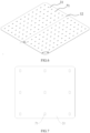
- the transparent support layer 7 includes transparent bumps 71, the transparent bumps 71 protrude from the surface of the back-contact solar cell 31, and the plurality of transparent bumps 71 are distributed at intervals on the surface of the back-contact solar cell 31.
- the transparent bumps 71 form scattered small-area shields on the front surface of the back-contact solar cell 31, thereby reducing the losses generated when the light passes through the transparent support layer 7.
- each transparent bump 71 can form a support point for the back-contact solar cell 31, and the plurality of transparent bumps 71 form scattered support points for the back-contact solar cell31, so as to provide stable support for the back-contact solar cell 31 and prevent shaking of the back-contact solar cell 31 during the transfer.
- the transparent bumps 71 are evenly distributed on the surface of the back-contact solar cell 31.
- the evenly distributed transparent bumps 71 can form uniform shields on the front surface of the back-contact solar cell 31, so that the incident light is uniformly distributed on the front surface of the back-contact solar cell 31.
- the evenly distributed transparent bumps 71 can form uniform support points on the front surface of the back-contact solar cell 31, so that each transparent bump 71 can bear a load evenly, which prevents local damages caused by an uneven force on the back-contact solar cell 31.
- the transparent bumps 71 may alternatively be unevenly distributed on the surface of the back-contact solar cell 31.
- the plurality of transparent bumps 71 may be unevenly distributed on the surface of the back-contact solar cell 31 in a random manner.
- the transparent bumps 71 are evenly distributed on the surface of the back-contact solar cell 31 according to a rectangular array, and two mutually perpendicular sides of the back-contact solar cell 31 respectively form rows and columns of the rectangular array, so that the arrangement of the transparent bumps 71 is compatible with the structure of the back-contact solar cell 31.
- the 9 transparent bumps 71 are distributed in a 3X3 rectangular array. That is, three transparent bumps 71 are arranged on each side of the back-contact solar cell 31, and one transparent bump 71 is arranged in the center, so as to form support for edge and central parts of the back-contact solar cell 31, which effectively prevent possible contact of the partial region of the back-contact solar cell 31 with the transfer table.
- a size of the back-contact solar cell 31 is small, and the number of the transparent bumps 71 is less than 9, for example 3.
- the plurality of transparent bumps 71 are unevenly distributed on the surface of the back-contact solar cell 31, so that each transparent bump 71 forms an effective region as large as possible, which reduces the number of the transparent bumps 71 on the surface of the back-contact solar cell 31, thereby reducing the light absorbed by the transparent bumps 71.
- An interval L between adjacent transparent bumps 71 is no greater than 7 cm.
- the interval between the adjacent transparent bumps 71 may be 7 cm, 6.5 cm, 6 cm, 5.5 cm, 5 cm, 4.5 cm, 4 cm, 3.5 cm, 3 cm, 2.5 cm, 2 cm, 1.5 cm, 1 cm, 0.5 cm, or the like, so that a small interval is kept between two adjacent support points, which effectively prevents the possible contact of the partial region of the back-contact solar cell 31 with the transfer table.
- the interval between the adjacent transparent bumps 71 is greater than 7 cm, a distance between two adjacent support points is excessively large, resulting in local damages due to easy contact of a part of the back-contact solar cell 31 between the two adjacent support points with the transfer table.
- a projected area of the transparent bumps 71 on the surface of the back-contact solar cell 31 is less than 10 mm 2 .
- the projected area of the transparent bumps 71 on the surface of the back-contact solar cell 31 may be 10 mm 2 , 9.5 mm 2 , 9 mm , 8.5 mm , 8 mm 2 , 7.5 mm 2 , 7 mm 2 , 6.5 mm 2 , 6 mm 2 , 5.5 mm 2 , 5 mm 2 , 4.5 mm 2 , 4 mm 2 , 3.5 mm 2 , 3 mm 2 , 2.5 mm 2 , 2 mm 2 , 1.5 mm 2 , 1 mm 2 , 0.5 mm 2 , or the like, which reduces absorption of the incident light by the transparent bumps 71 as much as possible and improves the conversion efficiency of the solar energy.
- a height of each of the transparent bumps 71 is less than 0.5 mm.
- the height of the transparent bump 71 may be 0.5 mm, 0.45 mm, 0.4 mm, 0.35 mm, 0.3 mm, 0.25 mm, 0.2 mm, 0.15 mm, 0.1 mm, 0.05 mm, or the like.
- the transparent bump 71 maintains high structural strength, thereby providing stable support for the back-contact solar cell 31.
- an influence of formation of pressure points inside the photovoltaic module by the transparent bumps 71 on an overall load capacity of the photovoltaic module is prevented.
- gaps there are gaps (i.e., D1 is greater than 0 and D2 is greater than 0 in the drawings) between the transparent bump 71 and edges of the back-contact solar cell 31, and when the back-contact solar cell 31 is required to be scribed, there is a gap (i.e., D3 is greater than 0 in the drawings) between the transparent bump 71 and a cutting line 32 of the back-contact solar cell 31, so as to prevent warping after the transparent bump 71 is cured and improve flatness of the transparent bump 71.
- the transparent support layer is made of any one of an insulating adhesive (any one of silicone, epoxy, and acrylic systems), a hot melt adhesive, PET, EVA, and POE, which can form better adhesion on the surface of the back-contact solar cell 31 and prevent damages such as delamination during lamination of the back-contact photovoltaic module, can have good light transmission, and produce no optical gain effect. That is, the transparent support layer is only light-transmitting and does not produce any optical gain effect, and the light passes through the transparent support layer and irradiates the surface of the back-contact solar cell 31, which is not significantly different from direct irradiation on the surface of the back-contact solar cell 31.
- an insulating adhesive any one of silicone, epoxy, and acrylic systems
- a hot melt adhesive PET, EVA, and POE
- the transparent support layer may alternatively be made of a material with an optical gain effect such as PVB, EPE, or EP, as long as the selected material has high adhesion and high transparency.
- a side of the upper adhesive film layer 2 facing the back-contact solar cell 31 is provided with a groove 21, and the groove 21 fits the transparent support layer. That is, the groove 21 is arranged at a position of the upper adhesive film layer 2 corresponding to the transparent support layer, a shape and a size of the groove 21 are adapted to those of the transparent support layer, and a depth of the groove 21 is adapted to a height of the transparent support layer, so that the transparent support layer can be stretched into the groove 21. Moreover, the groove 21 can be just filled up with the transparent support layer, so as to form a flat photovoltaic module structure. In addition, through the fitting between the groove 21 and the transparent support layer, positioning between the solar cell layer 3 and the upper adhesive film layer 2 can be achieved, which prevents slipping of the back-contact solar cell 31 during the lamination.
- some embodiments of the present disclosure provide a manufacturing method for a back-contact photovoltaic module.
- the back-contact photovoltaic module includes a glass substrate 1, an upper adhesive film layer 2, a solar cell layer 3, a lower adhesive film layer 4, and a back sheet 5 arranged in sequence from top to bottom.
- the solar cell layer 3 includes back-contact solar cells 31, a front surface of each of the back-contact solar cells 31 is provided with a transparent support layer, the transparent support layer protrudes from a surface of the back-contact solar cell 31, and the transparent support layer covers a partial region of the front surface.
- the manufacturing method includes: making the front surface of the back-contact solar cell 31 face upwards, and manufacturing the transparent support layer on the front surface of the back-contact solar cell 31; curing the transparent support layer; turning the back-contact solar cell 31 over for transfer; and packaging the back-contact solar cells 31 to form the back-contact photovoltaic module.
- the front surface of the back-contact solar cell 31 is provided with the transparent support layer, and the transparent support layer is made of a transparent material, so that incident light can pass therethrough smoothly.
- the transparent support layer protrudes from the surface of the back-contact solar cell 31, so that the transparent support layer can protect the front surface of the back-contact solar cell 31 and prevent direct contact of the surface of the back-contact solar cell 31 with the transfer table, thereby reducing a risk of scratches to the back-contact photovoltaic module.
- the transparent support layer covers the partial region of the front surface. That is, the transparent support layer does not completely cover the front surface of the back-contact solar cell 31, which further reduces absorption of the incident light by the transparent support layer, thereby improving the conversion efficiency of the solar energy.
- the transparent support layer may be manufactured on the front surface of the back-contact solar cell 31 by glue printing.
- the transparent support layer may be cured by thermosetting or photo-curing, or both.
- the packaging the back-contact solar cells 31 to form the back-contact photovoltaic module may include: printing and curing an insulating material on a back surface of the back-contact solar cell 31; printing and curing a conductive layer on the back surface of the back-contact solar cell 31; scribing; series welding; layout; and lamination.
- the frame 6 and the junction box may be further mounted after the lamination.
- the printing and curing of the insulating material on the back surface of the back-contact solar cell 31 realizes insulation between positive and negative electrodes and prevents a short circuit caused by contact of solder strips during soldering.
- the printing and curing of the conductive layer on the back surface of the back-contact solar cell 31 realizes interconnection of the back-contact solar cells 31. Scribing means reducing on-chip current transfer losses in the module by cutting the whole cell into small pieces.
Landscapes
- Photovoltaic Devices (AREA)
- Life Sciences & Earth Sciences (AREA)
- Engineering & Computer Science (AREA)
- Sustainable Development (AREA)
- Sustainable Energy (AREA)
Abstract
Description
- The present application claims priority to
Chinese Patent Application No. 202310458880.6, filed on April 24, 2023 - The present disclosure relates to the technical field of photovoltaic manufacturing, and in particular, to a back-contact photovoltaic module and a manufacturing method thereof.
- PN junctions and electrodes of a back-contact solar cell are located on a back surface of the cell. In other words, electrodes in emitter and base regions of the back-contact solar cell are all on the back surface, and a front surface is not shielded by gate lines, which can significantly improve photoelectric conversion performance of the solar cell and bring high cell efficiency and great development potential. Since the front surface of the back-contact solar cell is not shielded by the gate lines, a front film layer is directly in contact with a transfer table, which easily causes scratches during the transfer of the back-contact solar cell and affects an appearance of the solar cell.
- The present disclosure provides a back-contact photovoltaic module and a manufacturing method thereof, so as to protect the front surface of the back-contact solar cell and reduce a risk of scratches to the back-contact photovoltaic module.
- In a first aspect of the present disclosure, a back-contact photovoltaic module is provided, including a glass substrate, an upper adhesive film layer, a solar cell layer, a lower adhesive film layer, and a back sheet arranged in sequence from top to bottom; and
the solar cell layer includes back-contact solar cells, and a front surface of each of the back-contact solar cells is provided with a transparent support layer, the transparent support layer protruding from a surface of the back-contact solar cell, and the transparent support layer covering a partial region of the front surface. - In some embodiments, an area ratio of the transparent support layer to the front surface ranges from 1% to 80%.
- In some embodiments, the transparent support layer includes transparent bumps.
- In some embodiments, the transparent bumps are evenly distributed on the surface of the back-contact solar cell.
- In some embodiments, a number of the transparent bumps is equal to or more than 9;
or an interval between adjacent transparent bumps is equal to or less than 7 cm. - In some embodiments, a projected area of the transparent bumps on the surface of the back-contact solar cell is less than 10 mm2.
- In some embodiments, a height of each of the transparent bumps is less than 0.5 mm.
- In some embodiments, a gap is provided between each of the transparent bumps and an edge of each of the back-contact solar cells.
- In some embodiments, the transparent support layer is made of any one of an insulating adhesive, a hot melt adhesive, polyethylene terephthalate (PET), ethyl vinyl acetate (EVA), and polyolefin elastomer (POE).
- In some embodiments, a side of the upper adhesive film layer facing the back-contact solar cell is provided with a groove, the groove fitting the transparent support layer.
- In a second aspect of the present disclosure, a method for manufacturing a back-contact photovoltaic module is provided, wherein the back-contact photovoltaic module includes a glass substrate, an upper adhesive film layer, a solar cell layer, a lower adhesive film layer, and a back sheet arranged in sequence from top to bottom; and
- the solar cell layer includes back-contact solar cells, and a front surface of each of the back-contact solar cells is provided with a transparent support layer, the transparent support layer protruding from a surface of the back-contact solar cell, and the transparent support layer covering a partial region of the front surface; and the manufacturing method includes:
- making the front surface of the back-contact solar cell face upwards, and manufacturing the transparent support layer on the front surface of the back-contact solar cell; curing the transparent support layer; turning the back-contact solar cell over for transfer; and packaging the back-contact solar cells to form the back-contact photovoltaic module.
- It should be understood that the general description above and the detailed description in the following are merely exemplary, and cannot limit the present disclosure.
-
-
FIG. 1 is a schematic structural diagram of a back-contact photovoltaic module according to some embodiments of the present disclosure; -
FIG. 2 is a schematic structural diagram of a back-contact solar cell according to some embodiments of the present disclosure; -
FIG. 3 is a schematic structural diagram of a transparent support layer according to some embodiments of the present disclosure; -
FIG. 4 is another schematic structural diagram of a transparent support layer according to some embodiments of the present disclosure; -
FIG. 5 is a schematic structural diagram of a front surface of a back-contact solar cell according to some embodiments of the present disclosure; -
FIG. 6 is a schematic structural diagram of a front surface of another back-contact solar cell according to some embodiments of the present disclosure; -
FIG. 7 is a schematic diagram of a distribution structure of transparent bumps according to some embodiments of the present disclosure; -
FIG. 8 is a schematic diagram of another distribution structure of transparent bumps according to some embodiments of the present disclosure; -
FIG. 9 is a schematic diagram of a fitting structure of an upper adhesive film layer and a transparent support layer according to some embodiments of the present disclosure; and -
FIG. 10 is a flowchart of a back-contact photovoltaic module according to some embodiments of the present disclosure. -
- 1: glass substrate;
- 2: upper adhesive film layer;
21: groove; - 3: solar cell layer;
- 31: back-contact solar cell;
- 311: base;
- 312: doping layer;
- 3121: first doping region;
- 3122: second doping region;
- 313: first passivation layer;
- 314: first antireflection layer;
- 315: second passivation layer;
- 316: second antireflection layer;
- 317: first electrode;
- 318: second electrode;
- 32: cutting line;
- 31: back-contact solar cell;
- 4: lower adhesive film layer;
- 5: back sheet;
- 6: frame;
- 7: transparent support layer;
71: transparent bump. - The accompanying drawings herein, which are incorporated in and constitute a part of this specification, illustrate embodiments consistent with the present disclosure and, together with the specification, serve to explain principles of the present disclosure.
- In order to make the objectives, technical solutions, and advantages of the present disclosure clearer, the present disclosure is described in further detail below with reference to the accompanying drawings and embodiments. It should be understood that specific embodiments described herein are intended only to interpret the present disclosure and not intended to limit the present disclosure.
- In the description of the present disclosure, unless otherwise clearly stated and limited, the terms "first" and "second" are used for descriptive purposes only, which cannot be construed as indicating or implying a relative importance. Unless otherwise specified or stated, the term "a plurality of" means two or more. The terms "connection" and "fixing" should be understood in a broad sense. For example, "connection" may be a fixed connection, a detachable connection, or an integral connection; or an electrical connection; or a direct connection or an indirect connection through an intermediate medium. For those of ordinary skill in the art, the specific meanings of the foregoing terms in the present disclosure can be understood on a case-by-case basis.
- In the description of the present disclosure, it is to be understood that orientation terms such as "up" and "down" described in the embodiments of the present disclosure are described from the perspective shown in the accompanying drawings, and should not be construed as limiting the embodiments of the present disclosure. Besides, in this context, it is to be further understood that one element described as being connected "on" or "under" another element not only means that the element may be directly connected "on" or "under" the another element, but also means that the element may be indirectly connected "on" or "under" the another element through an intermediate element.
- As shown in
FIG. 1 to FIG. 9 , some embodiments of the present disclosure provide a back-contact photovoltaic module, including a glass substrate 1, an upperadhesive film layer 2, asolar cell layer 3, a loweradhesive film layer 4, and aback sheet 5 arranged in sequence from top to bottom. The glass substrate 1 and the upperadhesive film layer 2 are arranged on a front surface of the solar cell layer 3 (i.e., a light-receiving surface of the solar cell layer 3). The loweradhesive film layer 4 and theback sheet 5 are arranged on a back surface of the solar cell layer 3 (i.e., a backlight surface of the solar cell layer 3). The upperadhesive film layer 2 and the loweradhesive film layer 4 may be made of a same material or different materials. In some embodiments, the material includes EVA, POE, PVB, and the like. The glass substrate 1, the upperadhesive film layer 2, thesolar cell layer 3, the loweradhesive film layer 4, and theback sheet 5 are laminated and packaged to form a photovoltaic module that can be used outdoors for a long time. The back-contact photovoltaic module may further include aframe 6 and a junction box. Theframe 6 is arranged on an edge of the back-contact photovoltaic module to enhance structural strength of the module, prolong the service life of the module, and facilitate transportation, mounting, and fixing of the module. The junction box connects a circuit of the back-contact photovoltaic module and an external load circuit to realize transfer of electric energy. - In an embodiment, the
solar cell layer 3 includes back-contactsolar cells 31. Each back-contactsolar cell 31 includes a front surface and a back surface arranged oppositely. The back surface refers to a side of the back-contactsolar cell 31 provided with a gate line, and the front surface refers to a side of the back-contactsolar cell 31 provided with no gate line. - For example, referring to
FIG. 2 , the back-contactsolar cell 31 includes abase 311. A back surface of thebase 311 is sequentially provided with adoping layer 312, afirst passivation layer 313, and afirst antireflection layer 314, a front surface of thebase 311 is sequentially provided with asecond passivation layer 315 and asecond antireflection layer 316, thefirst antireflection layer 314 forms a surface of the front surface of the back-contactsolar cell 31, and thesecond antireflection layer 316 forms a surface of the back surface of the back-contactsolar cell 31. Thedoping layer 312 includes afirst doping region 3121 and asecond doping region 3122. Doping types of thefirst doping region 3121 and thesecond doping region 3122 are opposite. For example, thefirst doping region 3121 is an N-type doping region, and thesecond doping region 3122 is a P-type doping region. Thefirst doping region 3121 is connected to afirst electrode 317, and thefirst electrode 317 passes through thefirst passivation layer 313 and thefirst antireflection layer 314 and is exposed to the surface of the back-contact solar cell. Thesecond doping region 3122 is connected to asecond electrode 318, and thesecond electrode 318 passes through thefirst passivation layer 313 and thefirst antireflection layer 314 and is exposed to the surface of the back-contact solar cell. In some embodiments, a tunnel oxide layer and a doped polysilicon layer may also be provided between the base 311 and thedoping layer 312. One or more doped polysilicon layers are provided. - Referring to
FIG. 3 to FIG. 8 , further, the front surface of the back-contactsolar cell 31 is provided with atransparent support layer 7. That is, thetransparent support layer 7 is attached to the surface of the front surface of the back-contactsolar cell 31. The transparent support layer is only required to be manufactured on the front surface of the back-contactsolar cell 31 in a use process (for example, a process of using the back-contactsolar cell 31 to manufacture the photovoltaic module), without changing an original structure and a manufacturing process of the back-contactsolar cell 31, which can effectively reduce manufacturing costs. - In an embodiment, the
transparent support layer 7 is made of a transparent material, so that the incident light can pass therethrough smoothly. Thetransparent support layer 7 protrudes from the surface of the front surface of the back-contactsolar cell 31. When the front surface of the back-contactsolar cell 31 is transferred downwards, thetransparent support layer 7 separates the back-contactsolar cell 31 from a transfer table, thetransparent support layer 7 is in contact with the transfer table, and a gap is formed between the front surface of the back-contactsolar cell 31 and the transfer table, so that thetransparent support layer 7 protects the front surface of the back-contactsolar cell 31, which prevents direct contact of the surface of the back-contactsolar cell 31 with the transfer table, thereby reducing a risk of scratches to the back-contact photovoltaic module. - In an embodiment, the
transparent support layer 7 covers a partial region of the front surface. That is, thetransparent support layer 7 does not completely cover the front surface of the back-contactsolar cell 31. For example, thetransparent support layer 7 accounts for no more than 95% of an area of the front surface, which further reduces absorption of the incident light by thetransparent support layer 7, thereby improving conversion efficiency of solar energy. - Preferably, the
transparent support layer 7 accounts for 1% to 80% of the area of the front surface. For example, the transparent support layer accounts for 1%, 2%, 3%, 4%, 5%, 6%, 7%, 8%, 9%, 10%, 15%, 20%, 25%, 30%, 35%, 40%, 45%, 50%, 55%, 60%, 65%, 70%, 75%, or 80% of the area of the front surface, which can effectively protect the front surface of the back-contactsolar cell 31 and can also ensure that the front surface of the back-contactsolar cell 31 has sufficiently high transmittance, thereby improving the conversion efficiency of the solar energy. When thetransparent support layer 7 accounts for less than 1% of the area of the front surface, the area of thetransparent support layer 7 is excessively small. Due to influences of factors such as unevenness of the transfer table, possible bending of the back-contactsolar cell 31, and vibration or shaking generated during the transfer, thetransparent support layer 7 cannot effectively protect the front surface of the back-contactsolar cell 31, and the partial region of the front surface of the back-contactsolar cell 31 may still be in contact with the transfer table. When thetransparent support layer 7 accounts for more than 80% of the area of the front surface, the area of thetransparent support layer 7 is excessively large, so that great losses are generated when light passes through thetransparent support layer 7, resulting in low transmittance. - More preferably, the
transparent support layer 7 accounts for 2% to 30% of the area of the front surface. For example, thetransparent support layer 7 accounts for 2%, 3%, 4%, 5%, 6%, 7%, 8%, 9%, 10%, 12%, 15%, 18%, 20%, 23%, 25%, 28%, or 30% of the area of the front surface. Within the range, the front surface of the back-contactsolar cell 31 can be reliably protected, and the front surface of the back-contactsolar cell 31 can be guaranteed to have higher transmittance as much as possible, thereby improving the conversion efficiency of the solar energy. - The
transparent support layer 7 may be arranged as a continuous structure or a discrete structure. - When the
transparent support layer 7 is arranged as the continuous structure, thetransparent support layer 7 may be arranged in any suitable shape such as a rectangle, a circle, a ring, a zigzag, a curve or an irregular shape. Preferably, thetransparent support layer 7 is arranged as a rectangular structure (refer toFIG. 3 ) or a rectangular ring structure (refer toFIG. 4 ). Thetransparent support layer 7 is arranged in a center of the back-contactsolar cell 31, and a uniform interval is formed between an edge of thetransparent support layer 7 and an edge of the back-contactsolar cell 31, so that thetransparent support layer 7 can provide uniform and stable support for the back-contactsolar cell 31. - When the
transparent support layer 7 is arranged as the discrete structure, thetransparent support layer 7 may include support portions spaced apart from each other. Each support portion protrudes from the surface of the back-contactsolar cell 31, and the plurality of support portions jointly form thetransparent support layer 7. The plurality of support portions may be evenly distributed on the surface of the back-contactsolar cell 31 in a rectangular array or an annular array, and the plurality of support portions may alternatively be unevenly distributed on the surface of the back-contactsolar cell 31 in a random manner. It may be understood that each support portion may be arranged in any suitable shape such as a rectangle, a circle, a ring, a zigzag, a curve or an irregular shape. - Referring to
FIG. 5 to FIG. 8 , further, thetransparent support layer 7 includestransparent bumps 71, thetransparent bumps 71 protrude from the surface of the back-contactsolar cell 31, and the plurality oftransparent bumps 71 are distributed at intervals on the surface of the back-contactsolar cell 31. On the one hand, thetransparent bumps 71 form scattered small-area shields on the front surface of the back-contactsolar cell 31, thereby reducing the losses generated when the light passes through thetransparent support layer 7. On the other hand, eachtransparent bump 71 can form a support point for the back-contactsolar cell 31, and the plurality oftransparent bumps 71 form scattered support points for the back-contact solar cell31, so as to provide stable support for the back-contactsolar cell 31 and prevent shaking of the back-contactsolar cell 31 during the transfer. - In an embodiment, the
transparent bumps 71 are evenly distributed on the surface of the back-contactsolar cell 31. On the one hand, the evenly distributedtransparent bumps 71 can form uniform shields on the front surface of the back-contactsolar cell 31, so that the incident light is uniformly distributed on the front surface of the back-contactsolar cell 31. On the other hand, the evenly distributedtransparent bumps 71 can form uniform support points on the front surface of the back-contactsolar cell 31, so that eachtransparent bump 71 can bear a load evenly, which prevents local damages caused by an uneven force on the back-contactsolar cell 31. It may be understood that thetransparent bumps 71 may alternatively be unevenly distributed on the surface of the back-contactsolar cell 31. For example, the plurality oftransparent bumps 71 may be unevenly distributed on the surface of the back-contactsolar cell 31 in a random manner. - In some embodiments, referring to
FIG. 7 , thetransparent bumps 71 are evenly distributed on the surface of the back-contactsolar cell 31 according to a rectangular array, and two mutually perpendicular sides of the back-contactsolar cell 31 respectively form rows and columns of the rectangular array, so that the arrangement of thetransparent bumps 71 is compatible with the structure of the back-contactsolar cell 31. - When the plurality of
transparent bumps 71 are unevenly distributed according to the rectangular array, a number of thetransparent bumps 71 is no less than 9. Taking 9transparent bumps 71 as an example for detailed illustration, the 9transparent bumps 71 are distributed in a 3X3 rectangular array. That is, threetransparent bumps 71 are arranged on each side of the back-contactsolar cell 31, and onetransparent bump 71 is arranged in the center, so as to form support for edge and central parts of the back-contactsolar cell 31, which effectively prevent possible contact of the partial region of the back-contactsolar cell 31 with the transfer table. - In some other embodiments, referring to
FIG. 8 , a size of the back-contactsolar cell 31 is small, and the number of thetransparent bumps 71 is less than 9, for example 3. The plurality oftransparent bumps 71 are unevenly distributed on the surface of the back-contactsolar cell 31, so that eachtransparent bump 71 forms an effective region as large as possible, which reduces the number of thetransparent bumps 71 on the surface of the back-contactsolar cell 31, thereby reducing the light absorbed by the transparent bumps 71. An interval L between adjacenttransparent bumps 71 is no greater than 7 cm. For example, the interval between the adjacenttransparent bumps 71 may be 7 cm, 6.5 cm, 6 cm, 5.5 cm, 5 cm, 4.5 cm, 4 cm, 3.5 cm, 3 cm, 2.5 cm, 2 cm, 1.5 cm, 1 cm, 0.5 cm, or the like, so that a small interval is kept between two adjacent support points, which effectively prevents the possible contact of the partial region of the back-contactsolar cell 31 with the transfer table. When the interval between the adjacenttransparent bumps 71 is greater than 7 cm, a distance between two adjacent support points is excessively large, resulting in local damages due to easy contact of a part of the back-contactsolar cell 31 between the two adjacent support points with the transfer table. - In an embodiment, a projected area of the
transparent bumps 71 on the surface of the back-contactsolar cell 31 is less than 10 mm2. For example, the projected area of thetransparent bumps 71 on the surface of the back-contactsolar cell 31 may be 10 mm2, 9.5 mm2, 9 mm , 8.5 mm , 8 mm2, 7.5 mm2, 7 mm2, 6.5 mm2, 6 mm2, 5.5 mm2, 5 mm2, 4.5 mm2, 4 mm2, 3.5 mm2, 3 mm2, 2.5 mm2, 2 mm2, 1.5 mm2, 1 mm2, 0.5 mm2, or the like, which reduces absorption of the incident light by thetransparent bumps 71 as much as possible and improves the conversion efficiency of the solar energy. - In an embodiment, a height of each of the
transparent bumps 71 is less than 0.5 mm. For example, the height of thetransparent bump 71 may be 0.5 mm, 0.45 mm, 0.4 mm, 0.35 mm, 0.3 mm, 0.25 mm, 0.2 mm, 0.15 mm, 0.1 mm, 0.05 mm, or the like. On the one hand, thetransparent bump 71 maintains high structural strength, thereby providing stable support for the back-contactsolar cell 31. On the other hand, an influence of formation of pressure points inside the photovoltaic module by thetransparent bumps 71 on an overall load capacity of the photovoltaic module is prevented. - In an embodiment, referring to
FIG. 5 to FIG. 8 , there are gaps (i.e., D1 is greater than 0 and D2 is greater than 0 in the drawings) between thetransparent bump 71 and edges of the back-contactsolar cell 31, and when the back-contactsolar cell 31 is required to be scribed, there is a gap (i.e., D3 is greater than 0 in the drawings) between thetransparent bump 71 and acutting line 32 of the back-contactsolar cell 31, so as to prevent warping after thetransparent bump 71 is cured and improve flatness of thetransparent bump 71. - In an embodiment, the transparent support layer is made of any one of an insulating adhesive (any one of silicone, epoxy, and acrylic systems), a hot melt adhesive, PET, EVA, and POE, which can form better adhesion on the surface of the back-contact
solar cell 31 and prevent damages such as delamination during lamination of the back-contact photovoltaic module, can have good light transmission, and produce no optical gain effect. That is, the transparent support layer is only light-transmitting and does not produce any optical gain effect, and the light passes through the transparent support layer and irradiates the surface of the back-contactsolar cell 31, which is not significantly different from direct irradiation on the surface of the back-contactsolar cell 31. Therefore, an influence of the transparent support layer on the incident light can be reduced as much as possible, and uniformity of distribution of the incident light on the surface of the back-contactsolar cell 31 can be maintained. It may be understood that the transparent support layer may alternatively be made of a material with an optical gain effect such as PVB, EPE, or EP, as long as the selected material has high adhesion and high transparency. - In an embodiment, referring to
FIG. 9 , a side of the upperadhesive film layer 2 facing the back-contactsolar cell 31 is provided with agroove 21, and thegroove 21 fits the transparent support layer. That is, thegroove 21 is arranged at a position of the upperadhesive film layer 2 corresponding to the transparent support layer, a shape and a size of thegroove 21 are adapted to those of the transparent support layer, and a depth of thegroove 21 is adapted to a height of the transparent support layer, so that the transparent support layer can be stretched into thegroove 21. Moreover, thegroove 21 can be just filled up with the transparent support layer, so as to form a flat photovoltaic module structure. In addition, through the fitting between thegroove 21 and the transparent support layer, positioning between thesolar cell layer 3 and the upperadhesive film layer 2 can be achieved, which prevents slipping of the back-contactsolar cell 31 during the lamination. - As shown in
FIG. 10 , some embodiments of the present disclosure provide a manufacturing method for a back-contact photovoltaic module. The back-contact photovoltaic module includes a glass substrate 1, an upperadhesive film layer 2, asolar cell layer 3, a loweradhesive film layer 4, and aback sheet 5 arranged in sequence from top to bottom. Thesolar cell layer 3 includes back-contactsolar cells 31, a front surface of each of the back-contactsolar cells 31 is provided with a transparent support layer, the transparent support layer protrudes from a surface of the back-contactsolar cell 31, and the transparent support layer covers a partial region of the front surface. The manufacturing method includes: making the front surface of the back-contactsolar cell 31 face upwards, and manufacturing the transparent support layer on the front surface of the back-contactsolar cell 31; curing the transparent support layer; turning the back-contactsolar cell 31 over for transfer; and packaging the back-contactsolar cells 31 to form the back-contact photovoltaic module. - The front surface of the back-contact
solar cell 31 is provided with the transparent support layer, and the transparent support layer is made of a transparent material, so that incident light can pass therethrough smoothly. The transparent support layer protrudes from the surface of the back-contactsolar cell 31, so that the transparent support layer can protect the front surface of the back-contactsolar cell 31 and prevent direct contact of the surface of the back-contactsolar cell 31 with the transfer table, thereby reducing a risk of scratches to the back-contact photovoltaic module. The transparent support layer covers the partial region of the front surface. That is, the transparent support layer does not completely cover the front surface of the back-contactsolar cell 31, which further reduces absorption of the incident light by the transparent support layer, thereby improving the conversion efficiency of the solar energy. - In an embodiment, the transparent support layer may be manufactured on the front surface of the back-contact
solar cell 31 by glue printing. The transparent support layer may be cured by thermosetting or photo-curing, or both. - In an embodiment, the packaging the back-contact
solar cells 31 to form the back-contact photovoltaic module may include: printing and curing an insulating material on a back surface of the back-contactsolar cell 31; printing and curing a conductive layer on the back surface of the back-contactsolar cell 31; scribing; series welding; layout; and lamination. Theframe 6 and the junction box may be further mounted after the lamination. - The printing and curing of the insulating material on the back surface of the back-contact
solar cell 31 realizes insulation between positive and negative electrodes and prevents a short circuit caused by contact of solder strips during soldering. The printing and curing of the conductive layer on the back surface of the back-contactsolar cell 31 realizes interconnection of the back-contactsolar cells 31. Scribing means reducing on-chip current transfer losses in the module by cutting the whole cell into small pieces. - The above descriptions are only preferred embodiments of the present disclosure, and are not intended to limit the present disclosure. For those skilled in the art, various modifications and changes may be made to the present disclosure. Any modifications, equivalent replacements, improvements, and the like made within the spirit and the principle of the present disclosure shall fall within the protection scope of the present disclosure.
Claims (15)
- A back-contact photovoltaic module, comprising a glass substrate, an upper adhesive film layer, a solar cell layer, a lower adhesive film layer, and a back sheet arranged in sequence from top to bottom; and
wherein the solar cell layer comprises back-contact solar cells, and a front surface of each of the back-contact solar cells is provided with a transparent support layer, the transparent support layer protrudes from a surface of the back-contact solar cell, and the transparent support layer covers a partial region of the front surface. - The back-contact photovoltaic module according to claim 1, wherein an area ratio of the transparent support layer to the front surface ranges from 1% to 80%.
- The back-contact photovoltaic module according to claim 1, wherein the transparent support layer comprises transparent bumps.
- The back-contact photovoltaic module according to claim 3, wherein the transparent bumps are evenly distributed on the surface of the back-contact solar cell.
- The back-contact photovoltaic module according to claim 3, wherein a number of the transparent bumps is equal to or more than 9;
or an interval between adjacent transparent bumps is equal to or less than 7 cm. - The back-contact photovoltaic module according to claim 3, wherein a projected area of the transparent bumps on the surface of the back-contact solar cell is less than 10 mm2.
- The back-contact photovoltaic module according to claim 3, wherein a height of each of the transparent bumps is less than 0.5 mm.
- The back-contact photovoltaic module according to claim 3, wherein a gap is provided between each of the transparent bumps and an edge of each of the back-contact solar cells.
- The back-contact photovoltaic module according to claim 1, wherein the transparent support layer is made of any one of an insulating adhesive, a hot melt adhesive, polyethylene terephthalate (PET), ethyl vinyl acetate (EVA), and polyolefin elastomer (POE).
- The back-contact photovoltaic module according to claim 1, wherein a side of the upper adhesive film layer facing the back-contact solar cell is provided with a groove, and the groove fits the transparent support layer.
- A method for manufacturing a back-contact photovoltaic module, wherein the back-contact photovoltaic module comprises a glass substrate, an upper adhesive film layer, a solar cell layer, a lower adhesive film layer, and a back sheet arranged in sequence from top to bottom; andwherein the solar cell layer comprises back-contact solar cells, and a front surface of each of the back-contact solar cells is provided with a transparent support layer, the transparent support layer protrudes from a surface of the back-contact solar cell, and the transparent support layer covers a partial region of the front surface; andwherein the method comprises:making the front surface of the back-contact solar cell face upwards, and manufacturing the transparent support layer on the front surface of the back-contact solar cell;curing the transparent support layer;turning the back-contact solar cell over for transferring; andpackaging the back-contact solar cell to form the back-contact photovoltaic module.
- The back-contact photovoltaic module according to claim 11, wherein an area ratio of the transparent support layer to the front surface ranges from 1% to 80%.
- The back-contact photovoltaic module according to claim 11, wherein the transparent support layer comprises transparent bumps.
- The back-contact photovoltaic module according to claim 13, wherein the transparent bumps are evenly distributed on the surface of the back-contact solar cell.
- The back-contact photovoltaic module according to claim 13, wherein a number of the transparent bumps is equal to or more than 9;
or an interval between adjacent transparent bumps is equal to or less than 7 cm.
Priority Applications (1)
| Application Number | Priority Date | Filing Date | Title |
|---|---|---|---|
| EP26154818.4A EP4712736A2 (en) | 2023-04-24 | 2023-09-22 | Back-contact photovoltaic module and manufacturing method thereof |
Applications Claiming Priority (1)
| Application Number | Priority Date | Filing Date | Title |
|---|---|---|---|
| CN202310458880.6A CN116404050A (en) | 2023-04-24 | 2023-04-24 | Back-contact photovoltaic module and manufacturing method thereof |
Related Child Applications (2)
| Application Number | Title | Priority Date | Filing Date |
|---|---|---|---|
| EP26154818.4A Division-Into EP4712736A2 (en) | 2023-04-24 | 2023-09-22 | Back-contact photovoltaic module and manufacturing method thereof |
| EP26154818.4A Division EP4712736A2 (en) | 2023-04-24 | 2023-09-22 | Back-contact photovoltaic module and manufacturing method thereof |
Publications (2)
| Publication Number | Publication Date |
|---|---|
| EP4456152A1 true EP4456152A1 (en) | 2024-10-30 |
| EP4456152B1 EP4456152B1 (en) | 2026-04-15 |
Family
ID=87007466
Family Applications (2)
| Application Number | Title | Priority Date | Filing Date |
|---|---|---|---|
| EP23198994.8A Active EP4456152B1 (en) | 2023-04-24 | 2023-09-22 | Back-contact photovoltaic module and manufacturing method thereof |
| EP26154818.4A Pending EP4712736A2 (en) | 2023-04-24 | 2023-09-22 | Back-contact photovoltaic module and manufacturing method thereof |
Family Applications After (1)
| Application Number | Title | Priority Date | Filing Date |
|---|---|---|---|
| EP26154818.4A Pending EP4712736A2 (en) | 2023-04-24 | 2023-09-22 | Back-contact photovoltaic module and manufacturing method thereof |
Country Status (6)
| Country | Link |
|---|---|
| US (1) | US20240030365A1 (en) |
| EP (2) | EP4456152B1 (en) |
| JP (1) | JP7576138B1 (en) |
| CN (1) | CN116404050A (en) |
| AU (2) | AU2023233146B2 (en) |
| DE (1) | DE202023106524U1 (en) |
Families Citing this family (9)
| Publication number | Priority date | Publication date | Assignee | Title |
|---|---|---|---|---|
| AU2024291327A1 (en) * | 2023-07-04 | 2025-07-31 | Longi Solar Technology (Taizhou) Co., Ltd. | Cell, photovoltaic module, and packaging method for cell |
| CN220585238U (en) * | 2023-08-22 | 2024-03-12 | 珠海富山爱旭太阳能科技有限公司 | Back contact cell, cell module and photovoltaic system |
| CN117153951B (en) * | 2023-10-20 | 2024-07-19 | 正泰新能科技股份有限公司 | A production method of back-contact photovoltaic module and back-contact photovoltaic module |
| CN117438488B (en) * | 2023-12-21 | 2024-03-29 | 正泰新能科技股份有限公司 | Photovoltaic module and photovoltaic module preparation method |
| CN118507573A (en) * | 2024-01-29 | 2024-08-16 | 天合光能股份有限公司 | Solar cell, preparation method thereof, photovoltaic module and photovoltaic system |
| CN118156373A (en) * | 2024-05-08 | 2024-06-07 | 浙江晶科能源有限公司 | Photovoltaic module preparation method |
| CN119744027B (en) * | 2024-12-24 | 2025-07-25 | 隆基绿能科技股份有限公司 | Back contact battery and photovoltaic module |
| CN121924832A (en) * | 2025-09-15 | 2026-04-24 | 晶科能源(海宁)有限公司 | Back contact battery and photovoltaic module |
| CN121057353B (en) * | 2025-11-05 | 2026-02-10 | 苏州新维度微纳科技有限公司 | Methods for fabricating photovoltaic cell grid lines |
Citations (4)
| Publication number | Priority date | Publication date | Assignee | Title |
|---|---|---|---|---|
| CN1189949C (en) * | 1999-02-01 | 2005-02-16 | 库尔特玻璃+制镜股份公司 | Solar module |
| US20110014725A1 (en) * | 2008-01-31 | 2011-01-20 | Yoshiya Abiko | Method for manufacturing solar cell module |
| US9252299B2 (en) * | 2008-08-22 | 2016-02-02 | Panasonic Intellectual Property Management Co., Ltd. | Solar cell module, solar cell and solar cell module manufacturing method |
| CN218827167U (en) | 2022-08-01 | 2023-04-07 | 泰州隆基乐叶光伏科技有限公司 | Back contact battery piece and solar module |
Family Cites Families (7)
| Publication number | Priority date | Publication date | Assignee | Title |
|---|---|---|---|---|
| JP2008311604A (en) * | 2007-02-06 | 2008-12-25 | Hitachi Chem Co Ltd | Solar cell module and wavelength conversion type condensing film for solar cell module |
| JP5152858B2 (en) * | 2008-08-22 | 2013-02-27 | シャープ株式会社 | Solar cell module and manufacturing method thereof |
| US8933526B2 (en) * | 2009-07-15 | 2015-01-13 | First Solar, Inc. | Nanostructured functional coatings and devices |
| KR101131057B1 (en) * | 2010-08-02 | 2012-03-30 | 한국기계연구원 | High efficiency solar cell and method for manufacturing thereof |
| JP2013161980A (en) * | 2012-02-06 | 2013-08-19 | Nitto Denko Corp | Solar cell module, back surface electrode type solar cell element unit, and adhesive sheet |
| CN209804681U (en) * | 2018-12-28 | 2019-12-17 | 北京汉能光伏投资有限公司 | Solar cell module |
| CN218160393U (en) * | 2022-07-08 | 2022-12-27 | 晶澳(扬州)太阳能科技有限公司 | Solar cell and solar cell module thereof |
-
2023
- 2023-04-24 CN CN202310458880.6A patent/CN116404050A/en active Pending
- 2023-09-01 JP JP2023142572A patent/JP7576138B1/en active Active
- 2023-09-21 AU AU2023233146A patent/AU2023233146B2/en active Active
- 2023-09-22 EP EP23198994.8A patent/EP4456152B1/en active Active
- 2023-09-22 EP EP26154818.4A patent/EP4712736A2/en active Pending
- 2023-09-26 US US18/475,155 patent/US20240030365A1/en active Pending
- 2023-11-08 DE DE202023106524.4U patent/DE202023106524U1/en active Active
-
2025
- 2025-08-22 AU AU2025220860A patent/AU2025220860A1/en active Pending
Patent Citations (4)
| Publication number | Priority date | Publication date | Assignee | Title |
|---|---|---|---|---|
| CN1189949C (en) * | 1999-02-01 | 2005-02-16 | 库尔特玻璃+制镜股份公司 | Solar module |
| US20110014725A1 (en) * | 2008-01-31 | 2011-01-20 | Yoshiya Abiko | Method for manufacturing solar cell module |
| US9252299B2 (en) * | 2008-08-22 | 2016-02-02 | Panasonic Intellectual Property Management Co., Ltd. | Solar cell module, solar cell and solar cell module manufacturing method |
| CN218827167U (en) | 2022-08-01 | 2023-04-07 | 泰州隆基乐叶光伏科技有限公司 | Back contact battery piece and solar module |
Also Published As
| Publication number | Publication date |
|---|---|
| AU2023233146B2 (en) | 2025-05-22 |
| DE202023106524U1 (en) | 2024-02-07 |
| AU2025220860A1 (en) | 2025-09-11 |
| EP4456152B1 (en) | 2026-04-15 |
| US20240030365A1 (en) | 2024-01-25 |
| CN116404050A (en) | 2023-07-07 |
| JP2024159406A (en) | 2024-11-08 |
| JP7576138B1 (en) | 2024-10-30 |
| EP4712736A2 (en) | 2026-03-18 |
| AU2023233146A1 (en) | 2024-11-07 |
Similar Documents
| Publication | Publication Date | Title |
|---|---|---|
| EP4456152B1 (en) | Back-contact photovoltaic module and manufacturing method thereof | |
| US8039731B2 (en) | Photovoltaic concentrator for solar energy system | |
| US10879410B2 (en) | Solar cell module | |
| KR102323459B1 (en) | P-type PERC double-sided solar cell and its module, system and manufacturing method | |
| US20160268964A1 (en) | Solar cell module | |
| EP3067937B1 (en) | Solar cell module | |
| CN106098831A (en) | A kind of back contact solar cell string and preparation method thereof and assembly, system | |
| US20180366606A1 (en) | Solar cell module | |
| JP2016171299A (en) | Solar cell module | |
| KR20140098305A (en) | Solar cell module | |
| US20180294367A1 (en) | Back contact solar cell substrate, method of manufacturing the same and back contact solar cell | |
| US20170194525A1 (en) | High power solar cell module | |
| US10840402B2 (en) | Solar cell module | |
| US10784392B2 (en) | Solar cell module and method for manufacturing the same | |
| US20130306132A1 (en) | Solar photoelectrical module and fabrication thereof | |
| KR102196929B1 (en) | Solar cell module and rear substrate for the same | |
| US20150107649A1 (en) | Light Deflecting Layer For Photovoltaic Solar Panels | |
| US20230335657A1 (en) | Photovoltaic module | |
| US20180294370A1 (en) | Hybrid solar module | |
| JP2009147363A (en) | Solar cell module | |
| CN108780822B (en) | solar cell module | |
| JP4097549B2 (en) | Solar cell device and manufacturing method thereof | |
| JP2018056454A (en) | Solar cell module and method for manufacturing solar cell module | |
| CN206931606U (en) | P-type PERC double-sided solar batteries and its component, system | |
| CN220021136U (en) | Encapsulation cover plate and solar cell module |
Legal Events
| Date | Code | Title | Description |
|---|---|---|---|
| PUAI | Public reference made under article 153(3) epc to a published international application that has entered the european phase |
Free format text: ORIGINAL CODE: 0009012 |
|
| STAA | Information on the status of an ep patent application or granted ep patent |
Free format text: STATUS: REQUEST FOR EXAMINATION WAS MADE |
|
| 17P | Request for examination filed |
Effective date: 20230922 |
|
| AK | Designated contracting states |
Kind code of ref document: A1 Designated state(s): AL AT BE BG CH CY CZ DE DK EE ES FI FR GB GR HR HU IE IS IT LI LT LU LV MC ME MK MT NL NO PL PT RO RS SE SI SK SM TR |
|
| STAA | Information on the status of an ep patent application or granted ep patent |
Free format text: STATUS: EXAMINATION IS IN PROGRESS |
|
| TPAC | Observations filed by third parties |
Free format text: ORIGINAL CODE: EPIDOSNTIPA |
|
| 17Q | First examination report despatched |
Effective date: 20250613 |
|
| REG | Reference to a national code |
Ref country code: DE Free format text: PREVIOUS MAIN CLASS: H01L0031048000 Ref country code: DE Ref legal event code: R079 Ref document number: 602023015227 Country of ref document: DE Free format text: PREVIOUS MAIN CLASS: H01L0031048000 Ipc: H10F0077300000 |
|
| GRAP | Despatch of communication of intention to grant a patent |
Free format text: ORIGINAL CODE: EPIDOSNIGR1 |
|
| STAA | Information on the status of an ep patent application or granted ep patent |
Free format text: STATUS: GRANT OF PATENT IS INTENDED |
|
| RIC1 | Information provided on ipc code assigned before grant |
Ipc: H10F 77/30 20250101AFI20251205BHEP Ipc: H10F 19/80 20250101ALI20251205BHEP |
|
| INTG | Intention to grant announced |
Effective date: 20251218 |
|
| GRAS | Grant fee paid |
Free format text: ORIGINAL CODE: EPIDOSNIGR3 |
|
| GRAA | (expected) grant |
Free format text: ORIGINAL CODE: 0009210 |
|
| STAA | Information on the status of an ep patent application or granted ep patent |
Free format text: STATUS: THE PATENT HAS BEEN GRANTED |
|
| AK | Designated contracting states |
Kind code of ref document: B1 Designated state(s): AL AT BE BG CH CY CZ DE DK EE ES FI FR GB GR HR HU IE IS IT LI LT LU LV MC ME MK MT NL NO PL PT RO RS SE SI SK SM TR |
|
| REG | Reference to a national code |
Ref country code: CH Ref legal event code: F10 Free format text: ST27 STATUS EVENT CODE: U-0-0-F10-F00 (AS PROVIDED BY THE NATIONAL OFFICE) Effective date: 20260415 |