EP4456147A1 - Junction barrier schottky diode and method for manufacturing same - Google Patents
Junction barrier schottky diode and method for manufacturing same Download PDFInfo
- Publication number
- EP4456147A1 EP4456147A1 EP22911146.3A EP22911146A EP4456147A1 EP 4456147 A1 EP4456147 A1 EP 4456147A1 EP 22911146 A EP22911146 A EP 22911146A EP 4456147 A1 EP4456147 A1 EP 4456147A1
- Authority
- EP
- European Patent Office
- Prior art keywords
- type semiconductor
- semiconductor layer
- trenches
- semiconductor film
- diode
- Prior art date
- Legal status (The legal status is an assumption and is not a legal conclusion. Google has not performed a legal analysis and makes no representation as to the accuracy of the status listed.)
- Pending
Links
Images


Classifications
-
- H—ELECTRICITY
- H10—SEMICONDUCTOR DEVICES; ELECTRIC SOLID-STATE DEVICES NOT OTHERWISE PROVIDED FOR
- H10D—INORGANIC ELECTRIC SEMICONDUCTOR DEVICES
- H10D8/00—Diodes
- H10D8/60—Schottky-barrier diodes
-
- H—ELECTRICITY
- H10—SEMICONDUCTOR DEVICES; ELECTRIC SOLID-STATE DEVICES NOT OTHERWISE PROVIDED FOR
- H10D—INORGANIC ELECTRIC SEMICONDUCTOR DEVICES
- H10D8/00—Diodes
- H10D8/60—Schottky-barrier diodes
- H10D8/605—Schottky-barrier diodes of the trench conductor-insulator-semiconductor barrier type, e.g. trench MOS barrier Schottky rectifiers [TMBS]
-
- H—ELECTRICITY
- H10—SEMICONDUCTOR DEVICES; ELECTRIC SOLID-STATE DEVICES NOT OTHERWISE PROVIDED FOR
- H10D—INORGANIC ELECTRIC SEMICONDUCTOR DEVICES
- H10D62/00—Semiconductor bodies, or regions thereof, of devices having potential barriers
- H10D62/10—Shapes, relative sizes or dispositions of the regions of the semiconductor bodies; Shapes of the semiconductor bodies
- H10D62/102—Constructional design considerations for preventing surface leakage or controlling electric field concentration
- H10D62/103—Constructional design considerations for preventing surface leakage or controlling electric field concentration for increasing or controlling the breakdown voltage of reverse-biased devices
- H10D62/105—Constructional design considerations for preventing surface leakage or controlling electric field concentration for increasing or controlling the breakdown voltage of reverse-biased devices by having particular doping profiles, shapes or arrangements of PN junctions; by having supplementary regions, e.g. junction termination extension [JTE]
- H10D62/106—Constructional design considerations for preventing surface leakage or controlling electric field concentration for increasing or controlling the breakdown voltage of reverse-biased devices by having particular doping profiles, shapes or arrangements of PN junctions; by having supplementary regions, e.g. junction termination extension [JTE] having supplementary regions doped oppositely to or in rectifying contact with regions of the semiconductor bodies, e.g. guard rings with PN or Schottky junctions
-
- H—ELECTRICITY
- H10—SEMICONDUCTOR DEVICES; ELECTRIC SOLID-STATE DEVICES NOT OTHERWISE PROVIDED FOR
- H10D—INORGANIC ELECTRIC SEMICONDUCTOR DEVICES
- H10D62/00—Semiconductor bodies, or regions thereof, of devices having potential barriers
- H10D62/10—Shapes, relative sizes or dispositions of the regions of the semiconductor bodies; Shapes of the semiconductor bodies
- H10D62/124—Shapes, relative sizes or dispositions of the regions of semiconductor bodies or of junctions between the regions
- H10D62/125—Shapes of junctions between the regions
-
- H—ELECTRICITY
- H10—SEMICONDUCTOR DEVICES; ELECTRIC SOLID-STATE DEVICES NOT OTHERWISE PROVIDED FOR
- H10D—INORGANIC ELECTRIC SEMICONDUCTOR DEVICES
- H10D62/00—Semiconductor bodies, or regions thereof, of devices having potential barriers
- H10D62/80—Semiconductor bodies, or regions thereof, of devices having potential barriers characterised by the materials
- H10D62/82—Heterojunctions
- H10D62/8271—Heterojunctions comprising only oxide semiconductor materials heterojunctions, e.g. IGZO/IZO
-
- H—ELECTRICITY
- H10—SEMICONDUCTOR DEVICES; ELECTRIC SOLID-STATE DEVICES NOT OTHERWISE PROVIDED FOR
- H10D—INORGANIC ELECTRIC SEMICONDUCTOR DEVICES
- H10D62/00—Semiconductor bodies, or regions thereof, of devices having potential barriers
- H10D62/80—Semiconductor bodies, or regions thereof, of devices having potential barriers characterised by the materials
- H10D62/86—Semiconductor bodies, or regions thereof, of devices having potential barriers characterised by the materials being Group II-VI materials, e.g. ZnO
-
- H—ELECTRICITY
- H10—SEMICONDUCTOR DEVICES; ELECTRIC SOLID-STATE DEVICES NOT OTHERWISE PROVIDED FOR
- H10D—INORGANIC ELECTRIC SEMICONDUCTOR DEVICES
- H10D64/00—Electrodes of devices having potential barriers
- H10D64/20—Electrodes characterised by their shapes, relative sizes or dispositions
- H10D64/23—Electrodes carrying the current to be rectified, amplified, oscillated or switched, e.g. sources, drains, anodes or cathodes
-
- H—ELECTRICITY
- H10—SEMICONDUCTOR DEVICES; ELECTRIC SOLID-STATE DEVICES NOT OTHERWISE PROVIDED FOR
- H10D—INORGANIC ELECTRIC SEMICONDUCTOR DEVICES
- H10D8/00—Diodes
- H10D8/01—Manufacture or treatment
- H10D8/051—Manufacture or treatment of Schottky diodes
-
- H—ELECTRICITY
- H10—SEMICONDUCTOR DEVICES; ELECTRIC SOLID-STATE DEVICES NOT OTHERWISE PROVIDED FOR
- H10D—INORGANIC ELECTRIC SEMICONDUCTOR DEVICES
- H10D62/00—Semiconductor bodies, or regions thereof, of devices having potential barriers
- H10D62/80—Semiconductor bodies, or regions thereof, of devices having potential barriers characterised by the materials
- H10D62/82—Heterojunctions
-
- H—ELECTRICITY
- H10—SEMICONDUCTOR DEVICES; ELECTRIC SOLID-STATE DEVICES NOT OTHERWISE PROVIDED FOR
- H10D—INORGANIC ELECTRIC SEMICONDUCTOR DEVICES
- H10D62/00—Semiconductor bodies, or regions thereof, of devices having potential barriers
- H10D62/80—Semiconductor bodies, or regions thereof, of devices having potential barriers characterised by the materials
- H10D62/871—Semiconductor bodies, or regions thereof, of devices having potential barriers characterised by the materials being Group I-VI materials, e.g. Cu2O; being Group I-VII materials, e.g. CuI
Definitions
- the present invention relates to a junction barrier Schottky diode and a method for manufacturing the same.
- JBS diode which includes an n-type semiconductor layer formed on an n-type semiconductor substrate and having trenches opening on a surface opposite to the n-type semiconductor substrate, p-type semiconductor layers buried in the trenches of the n-type semiconductor layer, an anode electrode formed on the n-type semiconductor layer so as to be in contact with the p-type semiconductor layers, and a cathode electrode formed on a surface of the n-type semiconductor substrate opposite to the n-type semiconductor layer (see Patent Literature 1).
- JBS trench junction barrier Schottky
- Patent Literature 1 JP 2019/36593 A
- the electrical resistance of the p-type semiconductor layers is large because the p-type semiconductor layers are buried in the entire region in the trenches. Therefore, heat generated when a surge current occurs is large, and the connecting portions around the p-type semiconductor layers may be likely to be damaged. In other words, it may cause low surge resistance.
- the electrical resistance of the p-type semiconductor layer is high, it hinders the movement of charge necessary for charging/discharging for formation/disappearance of the depletion region near the pn junction, resulting in that energy losses during switching operations become large in some cases.
- an aspect of the present invention provides a junction barrier Schottky diode defined in (1) to (4) below and a method for manufacturing a junction barrier Schottky diode defined in (5) below.
- junction barrier Schottky diode with a trench structure that is excellent in surge resistance and exhibits suppressed energy losses during switching operations, and a method for manufacturing the same.
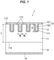
- FIG. 1 is a vertical cross-sectional view showing a junction barrier Schottky (JBS) diode 1 in an embodiment of the invention.
- the JBS diode 1 is a vertical JBS diode that has a trench structure.
- the JBS diode 1 includes an n-type semiconductor layer 11 having plural trenches 111 that open on a first surface 113, p-type semiconductor films 12 provided in contact with inner surfaces of the trenches 111 of the n-type semiconductor layer 11, an anode electrode 13 that is provided on the first surface 113 of the n-type semiconductor layer 11 so as to be in contact with mesa-shaped portions 112 between the plural trenches 111 of the n-type semiconductor layer 11 and has a portion 132 covered with the p-type semiconductor films 12 in the plural trenches 111, and a cathode electrode 14 provided, directly or through another layer, on a second surface 114 of the n-type semiconductor layer 11 opposite to the first surface 113.
- the JBS diode 1 includes an n-type semiconductor substrate 10 as a base for epitaxial growth of the n-type semiconductor layer 11, and the second surface 114 of the n-type semiconductor layer 11 is in contact with the n-type semiconductor substrate 10, as shown in FIG. 1 .
- the cathode electrode 14 is provided on a surface of the n-type semiconductor substrate 10 opposite to the n-type semiconductor layer 11. In other words, the cathode electrode 14 is provided on the second surface 114 of the n-type semiconductor layer 11 through the n-type semiconductor substrate 10.
- the n-type semiconductor layer 11 and the anode electrode 13 form a Schottky junction, and the JBS diode 1 uses the rectifying properties of this Schottky junction.
- a potential barrier at an interface between the anode electrode 13 and the n-type semiconductor layer 11 as viewed from the n-type semiconductor layer 11 is lowered by applying forward voltage between the anode electrode 13 and the cathode electrode 14 (positive potential on the anode electrode 13 side), allowing a current to flow from the anode electrode 13 to the cathode electrode 14.
- the JBS diode 1 in the present embodiment has a trench JBS structure and thus can have a high withstand voltage without an increase in resistance of the n-type semiconductor layer 11.
- the JBS diode 1 is a Schottky barrier diode having a high withstand voltage and low loss.
- the n-type semiconductor substrate 10 is formed of a single crystal of an n-type gallium oxide-based semiconductor containing a group IV element such as Si or Sn as a donor.
- a donor concentration in the n-type semiconductor substrate 10 is, e.g., not less than 1.0 ⁇ 10 16 cm -3 and not more than 1.0 ⁇ 10 22 cm -3 , preferably not less than 1.0 ⁇ 10 18 cm -3 and not more than 1.0 ⁇ 10 22 cm -3 .
- a thickness of the n-type semiconductor substrate 10 is, e.g., not less than 5 ⁇ m and not more than 650 ⁇ m.
- the gallium oxide-based semiconductor here is Ga 2 O 3 or is Ga 2 O 3 doped with one or both of Al and In, and has a composition represented by (Ga x Al y In (1-x-y) ) 2 O 3 (0 ⁇ x ⁇ 1, 0 ⁇ y ⁇ 1, 0 ⁇ x+y ⁇ 1).
- Ga 2 O 3 has a wider band gap when doped with Al and a narrower band gap when doped with In.
- the single crystal of the gallium oxide-based semiconductor mentioned above typically has a ⁇ -crystal structure.
- Ga 2 O 3 which is a typical example of gallium oxide-based semiconductor, has a band gap energy of 4.5 to 4.9 eV and a breakdown field strength of about 8.0 MV/cm.
- the n-type semiconductor layer 11 is formed of a single crystal of an n-type gallium oxide-based semiconductor containing a group IV element such as Si or Sn as a donor.
- a donor concentration in the n-type semiconductor layer 11 is lower than the donor concentration in the n-type semiconductor substrate 10.
- the n-type semiconductor layer 11 is, e.g., an epitaxial film epitaxially grown on the n-type semiconductor substrate 10.
- a high-donor-concentration layer containing a high concentration of donor may be formed between the n-type semiconductor substrate 10 and the n-type semiconductor layer 11.
- the high-donor-concentration layer is used in case where, e.g., the n-type semiconductor layer 11 is epitaxially grown on the n-type semiconductor substrate 10.
- the amount of dopant incorporated thereinto is unstable and an acceptor impurity is diffused from the n-type semiconductor substrate 10.
- resistance may increase in a region of the n-type semiconductor layer 11 close to the interface with the n-type semiconductor substrate 10 when the n-type semiconductor layer 11 is grown directly on the n-type semiconductor substrate 10.
- the high-donor-concentration layer is used to avoid such problems.
- a donor concentration in the high-donor-concentration layer is set to, e.g., higher than the donor concentration in the n-type semiconductor layer 11, and is more preferably set to not less than 10 times higher than the donor concentration in the n-type semiconductor layer 11.
- the donor concentration in the n-type semiconductor layer 11 is, e.g., not less than 2 ⁇ 10 14 cm -3 and not more than 4 ⁇ 10 17 cm -3 .
- the donor concentration in the n-type semiconductor layer 11 is preferably not more than 4 ⁇ 10 17 cm -3 , and more preferably, not less than 8 ⁇ 10 15 cm -3 and not more than 4 ⁇ 10 17 cm -3 .
- the donor concentration in the n-type semiconductor layer 11 is preferably not more than 1 ⁇ 10 17 cm -3 , and more preferably, not less than 2 ⁇ 10 15 cm -3 and not more than 1 ⁇ 10 17 cm -3 .
- the donor concentration in the n-type semiconductor layer 11 is preferably not more than 8 ⁇ 10 16 cm -3 , and more preferably, not less than 1.6 ⁇ 10 15 cm -3 and not more than 8 ⁇ 10 16 cm -3 .
- the donor concentration in the n-type semiconductor layer 11 is preferably not more than 5 ⁇ 10 16 cm -3 , and more preferably, not less than 1 ⁇ 10 15 cm -3 and not more than 5 ⁇ 10 16 cm -3 .
- the donor concentration in the n-type semiconductor layer 11 is preferably not more than 3 ⁇ 10 16 cm -3 , and more preferably, not less than 6 ⁇ 10 14 cm -3 and not more than 3 ⁇ 10 16 cm -3 .
- the donor concentration in the n-type semiconductor layer 11 is preferably not more than 1 ⁇ 10 16 cm -3 , and more preferably, not less than 2 ⁇ 10 14 cm -3 and not more than 1 ⁇ 10 16 cm -3 .
- the depth D of the trench 111 is preferably not less than 0.5 ⁇ m and not more than 5 ⁇ m.
- the thickness T of the n-type semiconductor layer 11 has, e.g., a value obtained by adding 0.5 to 110 ⁇ m to the depth D of the trench 111 measured from the first surface 113. And in order for the JBS diode 1 to have a withstand voltage of not less than 400 V, the thickness T of the n-type semiconductor layer 11 preferably has a value obtained by adding 0.6 to 9 ⁇ m to the depth D of the trench 111, more preferably has a value obtained by adding 0.6 to 6 ⁇ m.
- the thickness T of the n-type semiconductor layer 11 preferably has a value obtained by adding 0.8 to 11 ⁇ m to the depth D of the trench 111, more preferably has a value obtained by adding 0.8 to 7 ⁇ m.
- the thickness T of the n-type semiconductor layer 11 preferably has a value obtained by adding 1.5 to 20 ⁇ m to the depth D of the trench 111, more preferably has a value obtained by adding 1.5 to 12 ⁇ m.
- the thickness T of the n-type semiconductor layer 11 preferably has a value obtained by adding 4 to 40 ⁇ m to the depth D of the trench 111, more preferably has a value obtained by adding 4 to 25 ⁇ m.
- the thickness T of the n-type semiconductor layer 11 preferably has a value obtained by adding 5 to 50 ⁇ m to the depth D of the trench 111, more preferably has a value obtained by adding 5 to 30 ⁇ m.
- the thickness T of the n-type semiconductor layer 11 preferably has a value obtained by adding 7 to 90 ⁇ m to the depth D of the trench 111, more preferably has a value obtained by adding 7 to 55 ⁇ m.
- the thickness T of the n-type semiconductor layer 11 preferably has a value obtained by adding 12 to 180 ⁇ m to the depth D of the trench 111, more preferably has a value obtained by adding 12 to 110 ⁇ m.
- the width W m of the mesa-shaped portion 112 between adjacent trenches 111 of the n-type semiconductor layer 11 decreases, the electric field strength directly below the anode electrode 13 in the mesa-shaped portion 112 and the electric field strength at the junction between the n-type semiconductor layer 11 and the p-type semiconductor film 12 decrease.
- the width W m of the mesa-shaped section 112 is preferably not more than 5 ⁇ m.
- the width W m of the mesa-shaped portion 112 is preferably not less than 0.25 ⁇ m.
- the anode electrode 13 includes a portion 131 located outside the trenches 111 and the portion 132 located inside the trenches 111.
- the anode electrode 13 is configured such that a portion in contact with the n-type semiconductor layer 11 is formed of a material that forms a Schottky junction with the n-type semiconductor layer 11. That is, the anode electrode 13 when having a single layer structure is entirely formed of a material that forms a Schottky junction with the n-type semiconductor layer 11, and the anode electrode 13 when having a multilayer structure is configured such that at least a layer in contact with the n-type semiconductor layer 11 is formed of a material that forms a Schottky junction with the n-type semiconductor layer 11.
- the material of the portion of the anode electrode 13 that is in contact with the n-type semiconductor layer 11 it is possible to use, e.g., Pt, Ni, Au, Cu, Mo, W, Fe, Pd, or Cr, which forms a Schottky junction with the n-type semiconductor layer 11 formed of a gallium oxide-based semiconductor.
- the turn-on voltage of the JBS diode 1 is not less than 0.7 and not more than 1.2 V when using Pt or Ni as the material of the anode electrode 13, and the turn-on voltage of the JBS diode 1 is not less than 0.3 and not more than 0.8 V when using Mo as the material of anode electrode 13.
- the turn-on voltage depends on the width W m of the mesa-shaped portion 112 and increases as the width W m decreases.
- the field strength in the JBS diode 1 is affected by the width W m of the mesa portion 112 between two adjacent trenches 111 and the depth D of the trench 111, etc., as described above but is hardly affected by the planar pattern of the trenches 111.
- the planar pattern of the trenches 111 on the n-type semiconductor layer 11 is not specifically limited.
- the plural trenches 111 may be included in one continuous trench as long as the planar pattern of the trenches 111 is a planar pattern that forms the mesa-shaped portions 112 (e.g., a mesh pattern).
- the cathode electrode 14 is in ohmic contact with the n-type semiconductor substrate 10.
- the cathode electrode 14 is formed of a metal such as Ti.
- the cathode electrode 14 may have a multilayer structure formed by stacking different metal films, e.g., Ti/Au, Ti/Al, Ti/Ni/Au, or Ti/Al/Ni/Au.
- the cathode electrode 14 is preferably configured such that a layer in contact with the n-type semiconductor substrate 10 is formed of Ti.
- the cathode electrode 14 is in ohmic contact with the n-type semiconductor layer 11.
- the p-type semiconductor film 12 is used to improve the surge resistance of the JBS diode 1.
- the p-type semiconductor film 12 is a deposited film formed by deposition using a sputtering method or a CVD method, etc., and is not a region which is formed as part of the n-type semiconductor layer 11 by implanting an impurity into the inner surfaces of the trenches 111 using an ion implantation method.
- pn diodes have a higher on-voltage (forward turn-on voltage) than Schottky diodes. Therefore, it is possible to design so that a pn diode portion (a pn junction portion between the p-type semiconductor film 12 and the n-type semiconductor layer 11) does not turn on at the voltage at which the JBS diode 1 turns on. It is possible to design such that, e.g., the on-voltage of the JBS diode 1 is about 1 V and the on-voltage of the pn diode portion is about 2 V
- the p-type semiconductor film 12 is in the form of a film and thus has lower electrical resistance than a p-type semiconductor layer buried in the entire region in the trenches, such as the p-type semiconductor layer included in the trench JBS diode described in Patent Literature 1 mentioned above. Therefore, heat generated when a surge current occurs is small, and damage to the connecting portions around the p-type semiconductor film can be suppressed. In addition, since the electrical resistance of the p-type semiconductor film 12 is small, energy losses during switching operations of the JBS diode 1 can be suppressed.
- the p-type semiconductor film 12 is formed of a material that satisfies the condition represented by Expression 1 below so that a potential barrier is formed between itself and the n-type semiconductor layer 11.
- Expression 1 ⁇ p and ⁇ p are respectively electron affinity and work function of the p-type semiconductor which is the material of the p-type semiconductor film 12
- ⁇ n and ⁇ n are respectively electron affinity and work function of the n-type semiconductor which is the material of the n-type semiconductor layer 11.
- the work function mentioned above is the energy of the Fermi level as seen from the vacuum level.
- ⁇ n of Ga 2 O 3 which is a typical material of the n-type semiconductor layer 11, is about 4.0 eV, and ⁇ n varies depending on a carrier concentration in the n-type semiconductor layer 11 but is about 4.3 to 4.0 eV in the carrier concentration range of 1 ⁇ 10 14 cm -3 to 1 ⁇ 10 19 cm -3 .
- Materials which can be used as the material of the p-type semiconductor film 12 and can satisfy the condition represented by Expression 1 above are, e.g., p-type semiconductors such as Cu 2 O, NiO, Ag 2 O, polycrystalline Si, single crystal Si, amorphous Si, SnO, and CuO.
- p-type semiconductors such as Cu 2 O, NiO, Ag 2 O, polycrystalline Si, single crystal Si, amorphous Si, SnO, or CuO.
- Mixtures containing a p-type semiconductor such as Cu 2 O, NiO, Ag 2 O, polycrystalline Si, single crystal Si, amorphous Si, SnO, or CuO at a concentration sufficient to make the p-type semiconductor film 12 p-type can also be used as the material of the p-type semiconductor film 12.
- the p-type semiconductor as the material of the p-type semiconductor film 12 includes, e.g., Cu 2 O, NiO, Ag 2 O, polycrystalline Si, single crystal Si, amorphous Si, SnO, or CuO.
- Cu 2 O, NiO and SnO exhibit p-type conductivity without adding a dopant but may contain an acceptor impurity such as Li or nitrogen (N).
- Polycrystalline Si, single crystal Si, and amorphous Si preferably contain an acceptor impurity such as B or Al.
- a carrier concentration in the p-type semiconductor film 12 is preferably higher than the carrier concentration in the n-type semiconductor layer 11 so that the depletion layer generated in the p-type semiconductor film 12 from the interface with the n-type semiconductor layer 11 does not increase in thickness and reach the anode electrode 13 when reverse voltage is applied to the JBS diode 1.
- a thickness d of the p-type semiconductor film 12 preferably satisfies the condition represented by Expression 2 below to obtain the desired withstand voltage of the JBS diode 1.
- V BR is the desired withstand voltage (design withstand voltage)
- N D is the carrier concentration in the n-type semiconductor layer 11
- N A is the carrier concentration in the p-type semiconductor film 12
- ⁇ n is the electric permittivity of the n-type semiconductor layer 11
- q is the elementary charge.
- the withstand voltage of the JBS diode 1 can be not less than 1200 V when the thickness of the p-type semiconductor film 12 is not less than 200 nm.
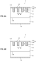
- FIGS. 2A and 2B are vertical cross-sectional views showing modifications of the p-type semiconductor film of the JBS diode 1.
- the height of the upper end of the p-type semiconductor film 12 does not need to match the height of the first surface 113. That is, the upper end of the p-type semiconductor film 12 may be higher than the first surface 113 as shown in FIG. 2A , and the upper end of the p-type semiconductor film 12 may be lower than the first surface 113 as shown in FIG. 2B .
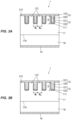
- FIGS. 3A and 3B are vertical cross-sectional views showing other modifications of the p-type semiconductor film of the JBS diode 1.
- the p-type semiconductor film 12 may be composed of a p-type semiconductor film 121 in contact with the inner surface of the trench 111, and a p-type semiconductor film 122 stacked thereon on the inner side.
- An impurity concentration in the p-type semiconductor film 122 is higher than an impurity concentration in the p-type semiconductor film 121.
- the carrier concentration limit determined by (Expression 2) above can be set lower than the carrier concentration limit determined by (Expression 2) above, hence, when reverse voltage is applied to the JBS diode 1, the electric field applied to trench corner portions of the p-type semiconductor film 121 and the n-type semiconductor layer 11 (the portions near the curved portions of the bottom edge of the trench 111) can be smaller than in the structure of FIG. 1 .
- the p-type semiconductor film 122 may have a shape which covers only around the bottom of the portion 132 of the anode electrode 13 inside the trench 111, as shown in FIG. 3B .
- the carrier concentration in the p-type semiconductor film 121 in the structure shown in FIG. 3B can be set lower than the carrier concentration limit determined by (Expression 2) above, hence, when reverse voltage is applied to the JBS diode 1, the electric field applied to the trench corner portions of the p-type semiconductor film 121 and the n-type semiconductor layer 11 can be smaller than in the structure of FIG. 1 .
- FIGS. 4A to 4C , 5A to 5C , 6A and 6B are explanatory vertical cross-sectional views showing a process of manufacturing the JBS diode 1 in the present embodiment.
- a single crystal of a gallium oxide-based semiconductor with a controlled donor concentration is epitaxially grown on the n-type semiconductor substrate 10 by a HVPE method, a CVD method, or an MBE method, etc., thereby forming an n-type semiconductor layer 11.
- plural trenches 111 are formed on the first surface 113 of the n-type semiconductor layer 11 by photolithography and dry etching, etc.
- the preferable conditions of the dry etching used to form the trenches 111 are, e.g., use of BCl 3 (30 sccm) as an etching gas, pressure of 1.0 Pa, antenna power of 160W, bias power of 17W, and duration of 90 minutes.
- a p-type semiconductor is deposited on the entire surface of the n-type semiconductor layer 11 on the first surface 113 side by a sputtering method or a CVD method, etc., thereby forming the p-type semiconductor film 12.
- the p-type semiconductor film 12 covers the inner surfaces of the trenches 111 and the first surface 113.
- Non-Patent Literature “Appl. Phys. Lett. 111, 093501 (2017), Fabrication and characterization of sputtered Cu 2 O:N/c-Si heterojunction diode”.
- NiO As the material of the p-type semiconductor film 12
- Non-Patent Literature “Appl. Phys. Lett. 117, 022104 (2020), A 1.86-kV double-layered NiO/ ⁇ -Ga 2 O 3 -vertical pn heterojunction diode”.
- polycrystalline Si, amorphous Si, or single crystal Si as the material of the p-type semiconductor film 12 it is possible to respectively use known deposition methods.
- a photoresist 20 is deposited on the entire surface of the p-type semiconductor film 12 by the spin coating method, etc., at least to the height where the voids in the trenched 111 are filled. At this time, deposition is performed so that the height difference between peaks and recesses on the surface of the photoresist 20 is smaller than the height difference between peaks and recesses on the p-type semiconductor film 12.
- the p-type semiconductor film 12 on the first surface 113 is exposed by etching back the photoresist 20.
- etching of the photoresist 20 e.g., a plasma asher device using oxygen plasma, etc., is used.
- the first surface 113 of the n-type semiconductor layer 11 is exposed by etching the p-type semiconductor film 12.
- the p-type semiconductor film 12 is formed of Cu 2 O
- a wet etching method using an acidic solution such as a buffered hydrofluoric acid solution, dilute hydrofluoric acid, diluted aqua regia, or dilute sulfuric acid, or a dry etching method can be used to etch the p-type semiconductor film 12, and the above wet etching method and the dry etching method can be used in combination.
- the photoresist 20 is removed.
- an organic chemical agent such as NMP or acetone is used to remove the photoresist 20.
- the anode electrode 13 is formed on the first surface 113 of the n-type semiconductor layer 11 so that the portion 132 thereof is covered with the p-type semiconductor films 12 in the plural trenches 111, and the cathode electrode 14 is formed on the bottom surface of the n-type semiconductor substrate 10.
- an electron beam evaporation method is used to form the anode electrode 13 and the cathode electrode 14.
- the p-type semiconductor film 12 is film that covers the inner surface of the trench 111. Therefore, as compared to when filling the trenches 111 with a p-type semiconductor, time required to deposit the material is shorter and the time required to remove the portion formed outside the trenches 111 is also shorter.
- the portion of the p-type semiconductor film 12 formed outside the trenches 111 is removed by the resist etch-back method using the photoresist 20 in the method described above but may be removed by polishing process such as CMP.
- the n-type semiconductor layer 11 may be formed of a material other than the gallium oxide-based semiconductor. Also in this case, electron affinity ⁇ n and work function ⁇ n of the material of the n-type semiconductor layer 11 and electron affinity ⁇ p and work function ⁇ p of the material of the p-type semiconductor film 12 satisfy the condition represented by Expression 1 above.
- the p-type semiconductor film 12 is a deposited film and is not formed as part of the n-type semiconductor layer 11 by ion implantation. Therefore, even when the n-type semiconductor layer 11 is formed of a material that is difficult to convert into p-type, such as a gallium oxide-based semiconductor, the p-type semiconductor film 12 can be formed using a material (base material) different from the n-type semiconductor layer 11.
- the n-type semiconductor layer 11 is preferably formed of, e.g., a material with a breakdown field strength of not less than 1 MV/cm or a band gap energy of not less than 1.
- gallium oxide-based semiconductor e.g., SiC with a breakdown field strength of 2.5 MV/cm and a band gap energy of 3.3 eV
- GaN with a breakdown field strength of 3.3 MV/cm and a band gap energy of 3.4 eV
- Al x In y Ga 1-x-y N with a breakdown field strength of 1.2 to 12 MV/cm and a band gap energy of 0.6 to 6.2 eV
- diamond with a breakdown field strength of about 8.0 MV/cm and a band gap energy of 5.5 eV can be used as the material of the n-type semiconductor layer 11.
- the n-type semiconductor substrate 10 may also be formed of a material other than the gallium oxide-based semiconductor.
- the same material as the n-type semiconductor layer 11 can be used as the material of the n-type semiconductor substrate 10.
- the JBS diode 1 with a trench structure that is excellent in surge resistance and exhibits suppressed energy losses during switching operations, and a method for manufacturing the same.
- the JBS diode 1 has high surge resistance and low turn-on voltage and can thus be suitably used in, e.g., a power converter circuit such as AC-DC converter.
- junction barrier Schottky diode with a trench structure that is excellent in surge resistance and exhibits suppressed energy losses during switching operations, and a method for manufacturing the same.
Landscapes
- Electrodes Of Semiconductors (AREA)
Abstract
Description
- The present invention relates to a junction barrier Schottky diode and a method for manufacturing the same.
- A trench junction barrier Schottky (JBS) diode is known which includes an n-type semiconductor layer formed on an n-type semiconductor substrate and having trenches opening on a surface opposite to the n-type semiconductor substrate, p-type semiconductor layers buried in the trenches of the n-type semiconductor layer, an anode electrode formed on the n-type semiconductor layer so as to be in contact with the p-type semiconductor layers, and a cathode electrode formed on a surface of the n-type semiconductor substrate opposite to the n-type semiconductor layer (see Patent Literature 1).
- In the trench JBS diode described in
Patent Literature 1, when reverse voltage is applied between the anode electrode and the cathode electrode, the current does not flow due to the Schottky barrier, and at this time, depletion layers spread from the p-type semiconductor layers and close channels between adjacent p-type semiconductor layers, hence, leakage current is effectively suppressed. - Patent Literature 1:
JP 2019/36593 A - In the trench JBS diode described in
Patent Literature 1, however, the electrical resistance of the p-type semiconductor layers is large because the p-type semiconductor layers are buried in the entire region in the trenches. Therefore, heat generated when a surge current occurs is large, and the connecting portions around the p-type semiconductor layers may be likely to be damaged. In other words, it may cause low surge resistance. In addition, if the electrical resistance of the p-type semiconductor layer is high, it hinders the movement of charge necessary for charging/discharging for formation/disappearance of the depletion region near the pn junction, resulting in that energy losses during switching operations become large in some cases. - It is an object of the invention to provide a junction barrier Schottky diode with a trench structure that is excellent in surge resistance and exhibits suppressed energy losses during switching operations, and a method for manufacturing the same.
- To achieve the above-mentioned object, an aspect of the present invention provides a junction barrier Schottky diode defined in (1) to (4) below and a method for manufacturing a junction barrier Schottky diode defined in (5) below.
- (1) Ajunction barrier Schottky diode, comprising:
- an n-type semiconductor layer comprising an n-type semiconductor and having a plurality of trenches that open on a first surface;
- a p-type semiconductor film comprising a p-type semiconductor and provided in contact with inner surfaces of the plurality of trenches;
- an anode electrode that is provided on the first surface of the n-type semiconductor layer so as to be in contact with a mesa-shaped portion between the plurality of trenches of the n-type semiconductor layer and comprises a portion covered with the p-type semiconductor film in the plurality of trenches; and
- a cathode electrode provided, directly or through another layer, on a second surface of the n-type semiconductor layer opposite to the first surface,
- wherein electron affinity χp and work function ϕp of the p-type semiconductor and electron affinity χn and work function ϕn of the n-type semiconductor satisfy a condition represented by an expression of the form χn - χp > ϕp - ϕn.
- (2) The junction barrier Schottky diode defined in (1), wherein the n-type semiconductor layer and the p-type semiconductor film comprise different semiconductors.
- (3) The junction barrier Schottky diode defined in (2), wherein the n-type semiconductor layer comprises a gallium oxide-based semiconductor.
- (4) The junction barrier Schottky diode defined in any one of (1) to (3), wherein the p-type semiconductor includes Cu2O, NiO, Ag2O, polycrystalline Si, single crystal Si, amorphous Si, SnO, or CuO.
- (5) A method for manufacturing a junction barrier Schottky diode, comprising:
- forming a plurality of trenches on a first surface of an n-type semiconductor layer that comprises an n-type semiconductor;
- forming a p-type semiconductor film that comprises a p-type semiconductor and is in contact with inner surfaces of the plurality of trenches;
- forming, on the first surface of the n-type semiconductor layer, an anode electrode that comprises a portion covered with the p-type semiconductor film in the plurality of trenches; and
- forming a cathode electrode, directly or through another layer, on a second surface of the n-type semiconductor layer opposite to the first surface,
- wherein electron affinity χp and work function ϕp of the p-type semiconductor and electron affinity χn and work function ϕn of the n-type semiconductor satisfy a condition represented by an expression of the form χn - χp > ϕp - ϕn.
- According to the invention, it is possible to provide a junction barrier Schottky diode with a trench structure that is excellent in surge resistance and exhibits suppressed energy losses during switching operations, and a method for manufacturing the same.
-
-
FIG. 1 is a vertical cross-sectional view showing a junction barrier Schottky (JBS) diode in an embodiment of the present invention. -
FIG. 2A is a vertical cross-sectional view showing a modification of a p-type semiconductor film of the JBS diode. -
FIG. 2B is a vertical cross-sectional view showing a modification of the p-type semiconductor film of the JBS diode. -
FIG. 3A is a vertical cross-sectional view showing another modification of the p-type semiconductor film of the JBS diode. -
FIG. 3B is a vertical cross-sectional view showing another modification of the p-type semiconductor film of the JBS diode. -
FIG. 4A is an explanatory vertical cross-sectional view showing a process of manufacturing the JBS diode in the embodiment. -
FIG. 4B is an explanatory vertical cross-sectional view showing the process of manufacturing the JBS diode in the embodiment. -
FIG. 4C is an explanatory vertical cross-sectional view showing the process of manufacturing the JBS diode in the embodiment. -
FIG. 5A is an explanatory vertical cross-sectional view showing the process of manufacturing the JBS diode in the embodiment. -
FIG. 5B is an explanatory vertical cross-sectional view showing the process of manufacturing the JBS diode in the embodiment. -
FIG. 5C is an explanatory vertical cross-sectional view showing the process of manufacturing the JBS diode in the embodiment. -
FIG. 6A is an explanatory vertical cross-sectional view showing the process of manufacturing the JBS diode in the embodiment. -
FIG. 6B is an explanatory vertical cross-sectional view showing the process of manufacturing the JBS diode in the embodiment. -
FIG. 1 is a vertical cross-sectional view showing a junction barrier Schottky (JBS)diode 1 in an embodiment of the invention. The JBSdiode 1 is a vertical JBS diode that has a trench structure. - The JBS
diode 1 includes an n-type semiconductor layer 11 havingplural trenches 111 that open on afirst surface 113, p-type semiconductor films 12 provided in contact with inner surfaces of thetrenches 111 of the n-type semiconductor layer 11, ananode electrode 13 that is provided on thefirst surface 113 of the n-type semiconductor layer 11 so as to be in contact with mesa-shaped portions 112 between theplural trenches 111 of the n-type semiconductor layer 11 and has aportion 132 covered with the p-type semiconductor films 12 in theplural trenches 111, and acathode electrode 14 provided, directly or through another layer, on asecond surface 114 of the n-type semiconductor layer 11 opposite to thefirst surface 113. - Typically, the JBS
diode 1 includes an n-type semiconductor substrate 10 as a base for epitaxial growth of the n-type semiconductor layer 11, and thesecond surface 114 of the n-type semiconductor layer 11 is in contact with the n-type semiconductor substrate 10, as shown inFIG. 1 . In this case, thecathode electrode 14 is provided on a surface of the n-type semiconductor substrate 10 opposite to the n-type semiconductor layer 11. In other words, thecathode electrode 14 is provided on thesecond surface 114 of the n-type semiconductor layer 11 through the n-type semiconductor substrate 10. - The n-
type semiconductor layer 11 and theanode electrode 13 form a Schottky junction, and theJBS diode 1 uses the rectifying properties of this Schottky junction. In theJBS diode 1, a potential barrier at an interface between theanode electrode 13 and the n-type semiconductor layer 11 as viewed from the n-type semiconductor layer 11 is lowered by applying forward voltage between theanode electrode 13 and the cathode electrode 14 (positive potential on theanode electrode 13 side), allowing a current to flow from theanode electrode 13 to thecathode electrode 14. - On the other hand, when reverse voltage is applied between the
anode electrode 13 and the cathode electrode 14 (negative potential on theanode electrode 13 side), the current does not flow due to the Schottky barrier. At this time, since depletion layers spread from the p-type semiconductor films 12 inside thetrenches 111 and close channels in the mesa-shapedportions 112 betweenadjacent trenches 111, leakage current is effectively suppressed. - The
JBS diode 1 in the present embodiment has a trench JBS structure and thus can have a high withstand voltage without an increase in resistance of the n-type semiconductor layer 11. In other words, theJBS diode 1 is a Schottky barrier diode having a high withstand voltage and low loss. - The n-
type semiconductor substrate 10 is formed of a single crystal of an n-type gallium oxide-based semiconductor containing a group IV element such as Si or Sn as a donor. A donor concentration in the n-type semiconductor substrate 10 is, e.g., not less than 1.0×1016 cm-3 and not more than 1.0×1022 cm-3, preferably not less than 1.0×1018 cm-3 and not more than 1.0×1022 cm-3. A thickness of the n-type semiconductor substrate 10 is, e.g., not less than 5 µm and not more than 650 µm. - The gallium oxide-based semiconductor here is Ga2O3 or is Ga2O3 doped with one or both of Al and In, and has a composition represented by (GaxAlyIn(1-x-y))2O3 (0<x≤1, 0≤y<1, 0<x+y≤1). Ga2O3 has a wider band gap when doped with Al and a narrower band gap when doped with In. The single crystal of the gallium oxide-based semiconductor mentioned above typically has a β-crystal structure. For example, Ga2O3, which is a typical example of gallium oxide-based semiconductor, has a band gap energy of 4.5 to 4.9 eV and a breakdown field strength of about 8.0 MV/cm.
- The n-
type semiconductor layer 11 is formed of a single crystal of an n-type gallium oxide-based semiconductor containing a group IV element such as Si or Sn as a donor. A donor concentration in the n-type semiconductor layer 11 is lower than the donor concentration in the n-type semiconductor substrate 10. The n-type semiconductor layer 11 is, e.g., an epitaxial film epitaxially grown on the n-type semiconductor substrate 10. - A high-donor-concentration layer containing a high concentration of donor may be formed between the n-
type semiconductor substrate 10 and the n-type semiconductor layer 11. The high-donor-concentration layer is used in case where, e.g., the n-type semiconductor layer 11 is epitaxially grown on the n-type semiconductor substrate 10. At the early growth stage of the n-type semiconductor layer 11, the amount of dopant incorporated thereinto is unstable and an acceptor impurity is diffused from the n-type semiconductor substrate 10. Thus, resistance may increase in a region of the n-type semiconductor layer 11 close to the interface with the n-type semiconductor substrate 10 when the n-type semiconductor layer 11 is grown directly on the n-type semiconductor substrate 10. The high-donor-concentration layer is used to avoid such problems. A donor concentration in the high-donor-concentration layer is set to, e.g., higher than the donor concentration in the n-type semiconductor layer 11, and is more preferably set to not less than 10 times higher than the donor concentration in the n-type semiconductor layer 11. - As the donor concentration in the n-
type semiconductor layer 11 increases, electrical field strength in each part of theJBS diode 1 increases. The donor concentration in the n-type semiconductor layer 11 is, e.g., not less than 2×1014 cm-3 and not more than 4×1017 cm-3. In order for theJBS diode 1 to have a withstand voltage of not less than 400 V, the donor concentration in the n-type semiconductor layer 11 is preferably not more than 4×1017 cm-3, and more preferably, not less than 8×1015 cm-3 and not more than 4×1017 cm-3. - In addition, in order for the
JBS diode 1 to have a withstand voltage of not less than 600 V, not more than 2×1017 cm-3 is preferable, and not less than 4×1015 cm-3 and not more than 2×1017 cm-3 is more preferable. In order for theJBS diode 1 to have a withstand voltage of not less than 1200 V, the donor concentration in the n-type semiconductor layer 11 is preferably not more than 1×1017 cm-3, and more preferably, not less than 2×1015 cm-3 and not more than 1×1017 cm-3. - In order for the
JBS diode 1 to have a withstand voltage of not less than 2200 V, the donor concentration in the n-type semiconductor layer 11 is preferably not more than 8×1016 cm-3, and more preferably, not less than 1.6×1015 cm-3 and not more than 8×1016 cm-3. In order for theJBS diode 1 to have a withstand voltage of not less than 3300 V, the donor concentration in the n-type semiconductor layer 11 is preferably not more than 5×1016 cm-3, and more preferably, not less than 1×1015 cm-3 and not more than 5×1016 cm-3. - In order for the
JBS diode 1 to have a withstand voltage of not less than 5000 V, the donor concentration in the n-type semiconductor layer 11 is preferably not more than 3×1016 cm-3, and more preferably, not less than 6×1014 cm-3 and not more than 3×1016 cm-3. In order for theJBS diode 1 to have a withstand voltage of not less than 10000 V, the donor concentration in the n-type semiconductor layer 11 is preferably not more than 1×1016 cm-3, and more preferably, not less than 2×1014 cm-3 and not more than 1×1016 cm-3. - When a thickness T of the n-
type semiconductor layer 11 is designed so that an electric field generated in each part when applying a reverse voltage equal to the design withstand voltage to theJBS diode 1 is smaller than the breakdown field, the larger the depth D of thetrench 111, the lower the electric field at the Schottky interface between theanode electrode 13 and thefirst surface 113 when reverse voltage is applied. On the other hand, if the depth D of thetrench 111 is too large, electrical resistance between theanode electrode 13 and thecathode electrode 14 of theJBS diode 1 increases. Thus, the depth D of thetrench 111 is preferably not less than 0.5 µm and not more than 5 µm. - The thickness T of the n-
type semiconductor layer 11 has, e.g., a value obtained by adding 0.5 to 110 µm to the depth D of thetrench 111 measured from thefirst surface 113. And in order for theJBS diode 1 to have a withstand voltage of not less than 400 V, the thickness T of the n-type semiconductor layer 11 preferably has a value obtained by adding 0.6 to 9 µm to the depth D of thetrench 111, more preferably has a value obtained by adding 0.6 to 6 µm. - Furthermore, in order for the
JBS diode 1 to have a withstand voltage of not less than 600 V, the thickness T of the n-type semiconductor layer 11 preferably has a value obtained by adding 0.8 to 11 µm to the depth D of thetrench 111, more preferably has a value obtained by adding 0.8 to 7 µm. In order for theJBS diode 1 to have a withstand voltage of not less than 1200 V, the thickness T of the n-type semiconductor layer 11 preferably has a value obtained by adding 1.5 to 20 µm to the depth D of thetrench 111, more preferably has a value obtained by adding 1.5 to 12 µm. - In order for the
JBS diode 1 to have a withstand voltage of not less than 2200 V, the thickness T of the n-type semiconductor layer 11 preferably has a value obtained by adding 4 to 40 µm to the depth D of thetrench 111, more preferably has a value obtained by adding 4 to 25 µm. In order for theJBS diode 1 to have a withstand voltage of not less than 3300 V, the thickness T of the n-type semiconductor layer 11 preferably has a value obtained by adding 5 to 50 µm to the depth D of thetrench 111, more preferably has a value obtained by adding 5 to 30 µm. - In order for the
JBS diode 1 to have a withstand voltage of not less than 5000 V, the thickness T of the n-type semiconductor layer 11 preferably has a value obtained by adding 7 to 90 µm to the depth D of thetrench 111, more preferably has a value obtained by adding 7 to 55 µm. In order for theJBS diode 1 to have a withstand voltage of not less than 10000 V, the thickness T of the n-type semiconductor layer 11 preferably has a value obtained by adding 12 to 180 µm to the depth D of thetrench 111, more preferably has a value obtained by adding 12 to 110 µm. - When a width Wt of the
trench 11 is narrower, the conduction loss can be more reduced but it is more difficult to manufacture, causing a decrease in production yield. Therefore, not less than 0.3 µm and not more than 5 µm is preferable. - As a width Wm of the mesa-shaped
portion 112 betweenadjacent trenches 111 of the n-type semiconductor layer 11 decreases, the electric field strength directly below theanode electrode 13 in the mesa-shapedportion 112 and the electric field strength at the junction between the n-type semiconductor layer 11 and the p-type semiconductor film 12 decrease. To effectively reduce these electric field strengths, the width Wm of the mesa-shapedsection 112 is preferably not more than 5 µm. On the other hand, the smaller the width Wm of the mesa-shapedportion 112, the more difficult it is to manufacture thetrench 111, hence, the width Wm of the mesa-shapedportion 112 is preferably not less than 0.25 µm. - The
anode electrode 13 includes aportion 131 located outside thetrenches 111 and theportion 132 located inside thetrenches 111. Theanode electrode 13 is configured such that a portion in contact with the n-type semiconductor layer 11 is formed of a material that forms a Schottky junction with the n-type semiconductor layer 11. That is, theanode electrode 13 when having a single layer structure is entirely formed of a material that forms a Schottky junction with the n-type semiconductor layer 11, and theanode electrode 13 when having a multilayer structure is configured such that at least a layer in contact with the n-type semiconductor layer 11 is formed of a material that forms a Schottky junction with the n-type semiconductor layer 11. - As the material of the portion of the
anode electrode 13 that is in contact with the n-type semiconductor layer 11, it is possible to use, e.g., Pt, Ni, Au, Cu, Mo, W, Fe, Pd, or Cr, which forms a Schottky junction with the n-type semiconductor layer 11 formed of a gallium oxide-based semiconductor. - In case that, e.g., the n-
type semiconductor layer 11 is formed of Ga2O3, the turn-on voltage of theJBS diode 1 is not less than 0.7 and not more than 1.2 V when using Pt or Ni as the material of theanode electrode 13, and the turn-on voltage of theJBS diode 1 is not less than 0.3 and not more than 0.8 V when using Mo as the material ofanode electrode 13. - In the
JBS diode 1, a potential barrier is formed in the mesa-shapedportion 112. Therefore, the turn-on voltage depends on the width Wm of the mesa-shapedportion 112 and increases as the width Wm decreases. - The field strength in the
JBS diode 1 is affected by the width Wm of themesa portion 112 between twoadjacent trenches 111 and the depth D of thetrench 111, etc., as described above but is hardly affected by the planar pattern of thetrenches 111. Thus, the planar pattern of thetrenches 111 on the n-type semiconductor layer 11 is not specifically limited. Theplural trenches 111 may be included in one continuous trench as long as the planar pattern of thetrenches 111 is a planar pattern that forms the mesa-shaped portions 112 (e.g., a mesh pattern). - When the
JBS diode 1 includes the n-type semiconductor substrate 10, thecathode electrode 14 is in ohmic contact with the n-type semiconductor substrate 10. Thecathode electrode 14 is formed of a metal such as Ti. Thecathode electrode 14 may have a multilayer structure formed by stacking different metal films, e.g., Ti/Au, Ti/Al, Ti/Ni/Au, or Ti/Al/Ni/Au. For reliable ohmic contact between thecathode electrode 14 and the n-type semiconductor substrate 10, thecathode electrode 14 is preferably configured such that a layer in contact with the n-type semiconductor substrate 10 is formed of Ti. When theJBS diode 1 does not include the n-type semiconductor substrate 10 and thecathode electrode 14 is directly connected to the n-type semiconductor layer 11, thecathode electrode 14 is in ohmic contact with the n-type semiconductor layer 11. - The p-
type semiconductor film 12 is used to improve the surge resistance of theJBS diode 1. The p-type semiconductor film 12 is a deposited film formed by deposition using a sputtering method or a CVD method, etc., and is not a region which is formed as part of the n-type semiconductor layer 11 by implanting an impurity into the inner surfaces of thetrenches 111 using an ion implantation method. - Normally, pn diodes have a higher on-voltage (forward turn-on voltage) than Schottky diodes. Therefore, it is possible to design so that a pn diode portion (a pn junction portion between the p-
type semiconductor film 12 and the n-type semiconductor layer 11) does not turn on at the voltage at which theJBS diode 1 turns on. It is possible to design such that, e.g., the on-voltage of theJBS diode 1 is about 1 V and the on-voltage of the pn diode portion is about 2 V - This allows for high-speed operation inherent to Schottky diode since the pn diode portion does not turn on during normal operation of the
JBS diode 1. On the other hand, when an inrush current occurs, the voltage of theJBS diode 1 rises and reaches the voltage at which the pn diode portion turns on, and current is injected from the p-type semiconductor film 12 to the n-type semiconductor layer 11. - At that time, resistance of a drift layer decreases and a large current called inrush current flows through
JBS diode 1 but the voltage rise is suppressed, hence, temperature rise is suppressed and damage to theJBS diode 1 due to inrush current can be prevented. - The p-
type semiconductor film 12 is in the form of a film and thus has lower electrical resistance than a p-type semiconductor layer buried in the entire region in the trenches, such as the p-type semiconductor layer included in the trench JBS diode described inPatent Literature 1 mentioned above. Therefore, heat generated when a surge current occurs is small, and damage to the connecting portions around the p-type semiconductor film can be suppressed. In addition, since the electrical resistance of the p-type semiconductor film 12 is small, energy losses during switching operations of theJBS diode 1 can be suppressed. - The p-
type semiconductor film 12 is formed of a material that satisfies the condition represented byExpression 1 below so that a potential barrier is formed between itself and the n-type semiconductor layer 11. InExpression 1, χp and ϕp are respectively electron affinity and work function of the p-type semiconductor which is the material of the p-type semiconductor film 12, and χn and ϕn are respectively electron affinity and work function of the n-type semiconductor which is the material of the n-type semiconductor layer 11. The work function mentioned above is the energy of the Fermi level as seen from the vacuum level. For example, χn of Ga2O3, which is a typical material of the n-type semiconductor layer 11, is about 4.0 eV, and ϕn varies depending on a carrier concentration in the n-type semiconductor layer 11 but is about 4.3 to 4.0 eV in the carrier concentration range of 1×1014 cm-3 to 1×1019 cm-3.
- Materials which can be used as the material of the p-
type semiconductor film 12 and can satisfy the condition represented byExpression 1 above are, e.g., p-type semiconductors such as Cu2O, NiO, Ag2O, polycrystalline Si, single crystal Si, amorphous Si, SnO, and CuO. Mixtures containing a p-type semiconductor such as Cu2O, NiO, Ag2O, polycrystalline Si, single crystal Si, amorphous Si, SnO, or CuO at a concentration sufficient to make the p-type semiconductor film 12 p-type can also be used as the material of the p-type semiconductor film 12. - That is, the p-type semiconductor as the material of the p-
type semiconductor film 12 includes, e.g., Cu2O, NiO, Ag2O, polycrystalline Si, single crystal Si, amorphous Si, SnO, or CuO. Cu2O, NiO and SnO exhibit p-type conductivity without adding a dopant but may contain an acceptor impurity such as Li or nitrogen (N). Polycrystalline Si, single crystal Si, and amorphous Si preferably contain an acceptor impurity such as B or Al. - A carrier concentration in the p-
type semiconductor film 12 is preferably higher than the carrier concentration in the n-type semiconductor layer 11 so that the depletion layer generated in the p-type semiconductor film 12 from the interface with the n-type semiconductor layer 11 does not increase in thickness and reach theanode electrode 13 when reverse voltage is applied to theJBS diode 1. - A thickness d of the p-
type semiconductor film 12 preferably satisfies the condition represented by Expression 2 below to obtain the desired withstand voltage of theJBS diode 1. In Expression 2, VBR is the desired withstand voltage (design withstand voltage), ND is the carrier concentration in the n-type semiconductor layer 11, NA is the carrier concentration in the p-type semiconductor film 12, εn is the electric permittivity of the n-type semiconductor layer 11, and q is the elementary charge.
- In case that, e.g., the carrier concentration in the n-
type semiconductor layer 11 formed of a gallium oxide-based semiconductor is 1×1016 cm-3 and the carrier concentration in the p-type semiconductor film 12 is 1×1019 cm-3, the withstand voltage of theJBS diode 1 can be not less than 1200 V when the thickness of the p-type semiconductor film 12 is not less than 200 nm. -
FIGS. 2A and 2B are vertical cross-sectional views showing modifications of the p-type semiconductor film of theJBS diode 1. In theJBS diode 1, the height of the upper end of the p-type semiconductor film 12 does not need to match the height of thefirst surface 113. That is, the upper end of the p-type semiconductor film 12 may be higher than thefirst surface 113 as shown inFIG. 2A , and the upper end of the p-type semiconductor film 12 may be lower than thefirst surface 113 as shown inFIG. 2B . -
FIGS. 3A and 3B are vertical cross-sectional views showing other modifications of the p-type semiconductor film of theJBS diode 1. As shown inFIG. 3A , the p-type semiconductor film 12 may be composed of a p-type semiconductor film 121 in contact with the inner surface of thetrench 111, and a p-type semiconductor film 122 stacked thereon on the inner side. An impurity concentration in the p-type semiconductor film 122 is higher than an impurity concentration in the p-type semiconductor film 121. A carrier concentration in the p-type semiconductor film 121 in the structure shown inFIG. 3A can be set lower than the carrier concentration limit determined by (Expression 2) above, hence, when reverse voltage is applied to theJBS diode 1, the electric field applied to trench corner portions of the p-type semiconductor film 121 and the n-type semiconductor layer 11 (the portions near the curved portions of the bottom edge of the trench 111) can be smaller than in the structure ofFIG. 1 . - Alternatively, the p-
type semiconductor film 122 may have a shape which covers only around the bottom of theportion 132 of theanode electrode 13 inside thetrench 111, as shown inFIG. 3B . Also in this case, the carrier concentration in the p-type semiconductor film 121 in the structure shown inFIG. 3B can be set lower than the carrier concentration limit determined by (Expression 2) above, hence, when reverse voltage is applied to theJBS diode 1, the electric field applied to the trench corner portions of the p-type semiconductor film 121 and the n-type semiconductor layer 11 can be smaller than in the structure ofFIG. 1 . - An example of a method for manufacturing the
JBS diode 1 will be described below. -
FIGS. 4A to 4C ,5A to 5C ,6A and 6B are explanatory vertical cross-sectional views showing a process of manufacturing theJBS diode 1 in the present embodiment. First, as shown inFIG. 4A , a single crystal of a gallium oxide-based semiconductor with a controlled donor concentration is epitaxially grown on the n-type semiconductor substrate 10 by a HVPE method, a CVD method, or an MBE method, etc., thereby forming an n-type semiconductor layer 11. - Next, as shown in
FIG. 4B ,plural trenches 111 are formed on thefirst surface 113 of the n-type semiconductor layer 11 by photolithography and dry etching, etc. The preferable conditions of the dry etching used to form thetrenches 111 are, e.g., use of BCl3 (30 sccm) as an etching gas, pressure of 1.0 Pa, antenna power of 160W, bias power of 17W, and duration of 90 minutes. - Next, as shown in
FIG. 4C , a p-type semiconductor is deposited on the entire surface of the n-type semiconductor layer 11 on thefirst surface 113 side by a sputtering method or a CVD method, etc., thereby forming the p-type semiconductor film 12. At this point, the p-type semiconductor film 12 covers the inner surfaces of thetrenches 111 and thefirst surface 113. - When using, e.g., Cu2O as the material of the p-
type semiconductor film 12, it is possible to use the method described in Non-Patent Literature "Appl. Phys. Lett. 111, 093501 (2017), Fabrication and characterization of sputtered Cu2O:N/c-Si heterojunction diode". When using NiO as the material of the p-type semiconductor film 12, it is possible to use the method described in Non-Patent Literature "Appl. Phys. Lett. 117, 022104 (2020), A 1.86-kV double-layered NiO/β-Ga2O3-vertical pn heterojunction diode". Furthermore, when using polycrystalline Si, amorphous Si, or single crystal Si as the material of the p-type semiconductor film 12, it is possible to respectively use known deposition methods. - Next, as shown in
FIG. 5A , aphotoresist 20 is deposited on the entire surface of the p-type semiconductor film 12 by the spin coating method, etc., at least to the height where the voids in the trenched 111 are filled. At this time, deposition is performed so that the height difference between peaks and recesses on the surface of thephotoresist 20 is smaller than the height difference between peaks and recesses on the p-type semiconductor film 12. - Next, as shown in
FIG. 5B , the p-type semiconductor film 12 on thefirst surface 113 is exposed by etching back thephotoresist 20. For etching of thephotoresist 20, e.g., a plasma asher device using oxygen plasma, etc., is used. - Next, as shown in
FIG. 5C , thefirst surface 113 of the n-type semiconductor layer 11 is exposed by etching the p-type semiconductor film 12. When, e.g., the p-type semiconductor film 12 is formed of Cu2O, a wet etching method using an acidic solution such as a buffered hydrofluoric acid solution, dilute hydrofluoric acid, diluted aqua regia, or dilute sulfuric acid, or a dry etching method can be used to etch the p-type semiconductor film 12, and the above wet etching method and the dry etching method can be used in combination. - Next, as shown in
FIG. 6A , thephotoresist 20 is removed. For example, an organic chemical agent such as NMP or acetone is used to remove thephotoresist 20. - Next, as shown in
FIG. 6B , theanode electrode 13 is formed on thefirst surface 113 of the n-type semiconductor layer 11 so that theportion 132 thereof is covered with the p-type semiconductor films 12 in theplural trenches 111, and thecathode electrode 14 is formed on the bottom surface of the n-type semiconductor substrate 10. For example, an electron beam evaporation method is used to form theanode electrode 13 and thecathode electrode 14. - The p-
type semiconductor film 12 is film that covers the inner surface of thetrench 111. Therefore, as compared to when filling thetrenches 111 with a p-type semiconductor, time required to deposit the material is shorter and the time required to remove the portion formed outside thetrenches 111 is also shorter. - In addition, the portion of the p-
type semiconductor film 12 formed outside thetrenches 111 is removed by the resist etch-back method using thephotoresist 20 in the method described above but may be removed by polishing process such as CMP. - The n-
type semiconductor layer 11 may be formed of a material other than the gallium oxide-based semiconductor. Also in this case, electron affinity χn and work function ϕn of the material of the n-type semiconductor layer 11 and electron affinity χp and work function ϕp of the material of the p-type semiconductor film 12 satisfy the condition represented byExpression 1 above. - As described above, the p-
type semiconductor film 12 is a deposited film and is not formed as part of the n-type semiconductor layer 11 by ion implantation. Therefore, even when the n-type semiconductor layer 11 is formed of a material that is difficult to convert into p-type, such as a gallium oxide-based semiconductor, the p-type semiconductor film 12 can be formed using a material (base material) different from the n-type semiconductor layer 11. - When the breakdown field strength of the n-
type semiconductor layer 11 is large, it is possible to have a large withstand voltage while suppressing an increase in on-resistance. For this reason, the n-type semiconductor layer 11 is preferably formed of, e.g., a material with a breakdown field strength of not less than 1 MV/cm or a band gap energy of not less than 1. - In addition to the gallium oxide-based semiconductor, e.g., SiC with a breakdown field strength of 2.5 MV/cm and a band gap energy of 3.3 eV, GaN with a breakdown field strength of 3.3 MV/cm and a band gap energy of 3.4 eV, AlxInyGa1-x-yN with a breakdown field strength of 1.2 to 12 MV/cm and a band gap energy of 0.6 to 6.2 eV, or diamond with a breakdown field strength of about 8.0 MV/cm and a band gap energy of 5.5 eV can be used as the material of the n-
type semiconductor layer 11. - The n-
type semiconductor substrate 10 may also be formed of a material other than the gallium oxide-based semiconductor. The same material as the n-type semiconductor layer 11 can be used as the material of the n-type semiconductor substrate 10. - According to the embodiment described above, it is possible to provide the
JBS diode 1 with a trench structure that is excellent in surge resistance and exhibits suppressed energy losses during switching operations, and a method for manufacturing the same. TheJBS diode 1 has high surge resistance and low turn-on voltage and can thus be suitably used in, e.g., a power converter circuit such as AC-DC converter. - Although the embodiment of the invention has been described, the invention is not intended to be limited to the embodiment, and the various kinds of modifications can be implemented without departing from the gist of the invention. In addition, the invention according to claims is not to be limited to the embodiment described above. Further, it should be noted that not all combinations of the features described in the embodiment are necessary to solve the problem of the invention.
- Provided are a junction barrier Schottky diode with a trench structure that is excellent in surge resistance and exhibits suppressed energy losses during switching operations, and a method for manufacturing the same.
-
- 1
- JUNCTION BARRIER SCHOTTKY DIODE
- 10
- N-TYPE SEMICONDUCTOR SUBSTRATE
- 11
- N-TYPE SEMICONDUCTOR LAYER
- 111
- TRENCH
- 112
- MESA-SHAPED PORTION
- 113
- FIRST SURFACE
- 114
- SECOND SURFACE
- 12
- P-TYPE SEMICONDUCTOR FILM
- 13
- ANODE ELECTRODE
- 14
- CATHODE ELECTRODE
Claims (5)
- A junction barrier Schottky diode, comprising:an n-type semiconductor layer comprising an n-type semiconductor and having a plurality of trenches that open on a first surface;a p-type semiconductor film comprising a p-type semiconductor and provided in contact with inner surfaces of the plurality of trenches;an anode electrode that is provided on the first surface of the n-type semiconductor layer so as to be in contact with a mesa-shaped portion between the plurality of trenches of the n-type semiconductor layer and comprises a portion covered with the p-type semiconductor film in the plurality of trenches; anda cathode electrode provided, directly or through another layer, on a second surface of the n-type semiconductor layer opposite to the first surface,wherein electron affinity χp and work function ϕp of the p-type semiconductor and electron affinity χn and work function ϕn of the n-type semiconductor satisfy a condition represented by an expression of the form χn - χp > ϕp - ϕn.
- The junction barrier Schottky diode according to claim 1, wherein the n-type semiconductor layer and the p-type semiconductor film comprise different semiconductors.
- The junction barrier Schottky diode according to claim 2, wherein the n-type semiconductor layer comprises a gallium oxide-based semiconductor.
- The junction barrier Schottky diode according to any one of claims 1 to 3, wherein the p-type semiconductor includes Cu2O, NiO, Ag2O, polycrystalline Si, single crystal Si, amorphous Si, SnO, or CuO.
- A method for manufacturing a junction barrier Schottky diode, comprising:forming a plurality of trenches on a first surface of an n-type semiconductor layer that comprises an n-type semiconductor;forming a p-type semiconductor film that comprises a p-type semiconductor and is in contact with inner surfaces of the plurality of trenches;forming, on the first surface of the n-type semiconductor layer, an anode electrode that comprises a portion covered with the p-type semiconductor film in the plurality of trenches; andforming a cathode electrode, directly or through another layer, on a second surface of the n-type semiconductor layer opposite to the first surface,wherein electron affinity χp and work function ϕp of the p-type semiconductor and electron affinity χn and work function ϕn of the n-type semiconductor satisfy a condition represented by an expression of the form χn - χp > ϕp - ϕn.
Applications Claiming Priority (2)
| Application Number | Priority Date | Filing Date | Title |
|---|---|---|---|
| JP2021210457A JP2023094888A (en) | 2021-12-24 | 2021-12-24 | Junction barrier Schottky diode and manufacturing method thereof |
| PCT/JP2022/046558 WO2023120443A1 (en) | 2021-12-24 | 2022-12-17 | Junction barrier schottky diode and method for manufacturing same |
Publications (2)
| Publication Number | Publication Date |
|---|---|
| EP4456147A1 true EP4456147A1 (en) | 2024-10-30 |
| EP4456147A4 EP4456147A4 (en) | 2025-11-26 |
Family
ID=86902410
Family Applications (1)
| Application Number | Title | Priority Date | Filing Date |
|---|---|---|---|
| EP22911146.3A Pending EP4456147A4 (en) | 2021-12-24 | 2022-12-17 | Barrier layer Schottky diode and method for its manufacture |
Country Status (6)
| Country | Link |
|---|---|
| US (1) | US20250386528A1 (en) |
| EP (1) | EP4456147A4 (en) |
| JP (1) | JP2023094888A (en) |
| CN (1) | CN118435360A (en) |
| TW (1) | TW202329251A (en) |
| WO (1) | WO2023120443A1 (en) |
Families Citing this family (1)
| Publication number | Priority date | Publication date | Assignee | Title |
|---|---|---|---|---|
| CN119451139A (en) * | 2024-10-31 | 2025-02-14 | 中国电子科技集团公司第五十八研究所 | A trench-type gallium oxide heterojunction barrier Schottky diode |
Family Cites Families (7)
| Publication number | Priority date | Publication date | Assignee | Title |
|---|---|---|---|---|
| JP5103683B2 (en) * | 2007-11-21 | 2012-12-19 | 日本軽金属株式会社 | Method of manufacturing electrode for gallium oxide substrate and electrode for gallium oxide substrate manufactured thereby |
| JP2012234949A (en) * | 2011-04-28 | 2012-11-29 | Panasonic Corp | Solid state imaging device and manufacturing method therefor |
| JP5607676B2 (en) * | 2012-04-17 | 2014-10-15 | 国立大学法人電気通信大学 | Rectifier element |
| CN106415845B (en) * | 2014-07-22 | 2019-12-10 | 株式会社Flosfia | Crystalline semiconductor film, plate-like body, and semiconductor device |
| JP7037142B2 (en) * | 2017-08-10 | 2022-03-16 | 株式会社タムラ製作所 | diode |
| DE112018007055B4 (en) * | 2018-02-09 | 2024-02-01 | Mitsubishi Electric Corporation | Power semiconductor unit |
| JP7382559B2 (en) * | 2019-12-25 | 2023-11-17 | 株式会社ノベルクリスタルテクノロジー | Trench MESFET |
-
2021
- 2021-12-24 JP JP2021210457A patent/JP2023094888A/en active Pending
-
2022
- 2022-12-17 US US18/723,653 patent/US20250386528A1/en active Pending
- 2022-12-17 CN CN202280085639.7A patent/CN118435360A/en active Pending
- 2022-12-17 WO PCT/JP2022/046558 patent/WO2023120443A1/en not_active Ceased
- 2022-12-17 EP EP22911146.3A patent/EP4456147A4/en active Pending
- 2022-12-20 TW TW111148851A patent/TW202329251A/en unknown
Also Published As
| Publication number | Publication date |
|---|---|
| US20250386528A1 (en) | 2025-12-18 |
| EP4456147A4 (en) | 2025-11-26 |
| TW202329251A (en) | 2023-07-16 |
| WO2023120443A1 (en) | 2023-06-29 |
| JP2023094888A (en) | 2023-07-06 |
| CN118435360A (en) | 2024-08-02 |
Similar Documents
| Publication | Publication Date | Title |
|---|---|---|
| EP3667737B1 (en) | Diode | |
| CN110112207B (en) | A kind of gallium oxide-based hybrid PiN Schottky diode and preparation method thereof | |
| JP5011069B2 (en) | Low voltage diode with small parasitic resistance and manufacturing method | |
| US20190140046A1 (en) | Silicon carbide power device employing heterojunction terminal and manufacturing method thereof | |
| KR101412802B1 (en) | Semiconductor device having surge current protection and method of manufacturing the same | |
| TWI798402B (en) | Schottky barrier diode | |
| US11923464B2 (en) | Schottky barrier diode | |
| US20130140584A1 (en) | Semiconductor device | |
| EP3703137A1 (en) | Schottky barrier diode | |
| CN113725296B (en) | Nitride semiconductor epitaxial lamination structure and power element thereof | |
| CN103930974A (en) | Method for Fabricating GaN Hybrid P-I-N Schottky (MPS) Diodes | |
| US8823148B2 (en) | Diode with epitaxially grown semiconductor layers | |
| US11923463B2 (en) | Power Schottky barrier diodes with high breakdown voltage and low leakage current | |
| US20130119437A1 (en) | Semiconductor device | |
| US11456388B2 (en) | Trench MOS schottky diode and method for producing same | |
| US11424357B2 (en) | Semiconductor device | |
| US20250386528A1 (en) | Junction barrier schottky diode and method for manufacturing same | |
| JP5140998B2 (en) | Wide band gap semiconductor device and method of manufacturing the same | |
| CN121099620A (en) | Semiconductor structure and manufacturing method thereof | |
| EP4632822A1 (en) | Junction barrier schottky diode and production method therefor | |
| US12532488B2 (en) | Semiconductor device with selectively grown field oxide layer in edge termination region | |
| CN118016665A (en) | Enhancement-mode GaN HEMT on SiC substrate with integrated SBD |
Legal Events
| Date | Code | Title | Description |
|---|---|---|---|
| STAA | Information on the status of an ep patent application or granted ep patent |
Free format text: STATUS: THE INTERNATIONAL PUBLICATION HAS BEEN MADE |
|
| PUAI | Public reference made under article 153(3) epc to a published international application that has entered the european phase |
Free format text: ORIGINAL CODE: 0009012 |
|
| STAA | Information on the status of an ep patent application or granted ep patent |
Free format text: STATUS: REQUEST FOR EXAMINATION WAS MADE |
|
| 17P | Request for examination filed |
Effective date: 20240724 |
|
| AK | Designated contracting states |
Kind code of ref document: A1 Designated state(s): AL AT BE BG CH CY CZ DE DK EE ES FI FR GB GR HR HU IE IS IT LI LT LU LV MC ME MK MT NL NO PL PT RO RS SE SI SK SM TR |
|
| DAV | Request for validation of the european patent (deleted) | ||
| DAX | Request for extension of the european patent (deleted) | ||
| REG | Reference to a national code |
Ref country code: DE Ref legal event code: R079 Free format text: PREVIOUS MAIN CLASS: H01L0029872000 Ipc: H10D0008600000 |
|
| A4 | Supplementary search report drawn up and despatched |
Effective date: 20251029 |
|
| RIC1 | Information provided on ipc code assigned before grant |
Ipc: H10D 8/60 20250101AFI20251023BHEP Ipc: H10D 8/01 20250101ALI20251023BHEP Ipc: H10D 64/64 20250101ALI20251023BHEP Ipc: H10D 8/00 20250101ALI20251023BHEP Ipc: H10D 8/50 20250101ALI20251023BHEP Ipc: H10D 62/10 20250101ALI20251023BHEP Ipc: H10D 62/82 20250101ALI20251023BHEP Ipc: H10D 64/23 20250101ALN20251023BHEP |