EP4456072A2 - Speicherzugrifflatenzschätzverfahren und speicherzugrifflatenzschätzsystem zur schätzung einer speicherzugrifflatenz nach mehreren koeffizienten und indizes - Google Patents
Speicherzugrifflatenzschätzverfahren und speicherzugrifflatenzschätzsystem zur schätzung einer speicherzugrifflatenz nach mehreren koeffizienten und indizes Download PDFInfo
- Publication number
- EP4456072A2 EP4456072A2 EP24172130.7A EP24172130A EP4456072A2 EP 4456072 A2 EP4456072 A2 EP 4456072A2 EP 24172130 A EP24172130 A EP 24172130A EP 4456072 A2 EP4456072 A2 EP 4456072A2
- Authority
- EP
- European Patent Office
- Prior art keywords
- memory
- indexes
- coefficients
- latency
- access
- Prior art date
- Legal status (The legal status is an assumption and is not a legal conclusion. Google has not performed a legal analysis and makes no representation as to the accuracy of the status listed.)
- Pending
Links
Images



Classifications
-
- G—PHYSICS
- G11—INFORMATION STORAGE
- G11C—STATIC STORES
- G11C29/00—Checking stores for correct operation ; Subsequent repair; Testing stores during standby or offline operation
- G11C29/02—Detection or location of defective auxiliary circuits, e.g. defective refresh counters
- G11C29/028—Detection or location of defective auxiliary circuits, e.g. defective refresh counters with adaption or trimming of parameters
-
- G—PHYSICS
- G06—COMPUTING OR CALCULATING; COUNTING
- G06F—ELECTRIC DIGITAL DATA PROCESSING
- G06F3/00—Input arrangements for transferring data to be processed into a form capable of being handled by the computer; Output arrangements for transferring data from processing unit to output unit, e.g. interface arrangements
- G06F3/06—Digital input from, or digital output to, record carriers, e.g. RAID, emulated record carriers or networked record carriers
- G06F3/0601—Interfaces specially adapted for storage systems
- G06F3/0602—Interfaces specially adapted for storage systems specifically adapted to achieve a particular effect
- G06F3/0625—Power saving in storage systems
-
- G—PHYSICS
- G06—COMPUTING OR CALCULATING; COUNTING
- G06F—ELECTRIC DIGITAL DATA PROCESSING
- G06F13/00—Interconnection of, or transfer of information or other signals between, memories, input/output devices or central processing units
- G06F13/14—Handling requests for interconnection or transfer
- G06F13/16—Handling requests for interconnection or transfer for access to memory bus
- G06F13/1605—Handling requests for interconnection or transfer for access to memory bus based on arbitration
- G06F13/161—Handling requests for interconnection or transfer for access to memory bus based on arbitration with latency improvement
-
- G—PHYSICS
- G06—COMPUTING OR CALCULATING; COUNTING
- G06F—ELECTRIC DIGITAL DATA PROCESSING
- G06F13/00—Interconnection of, or transfer of information or other signals between, memories, input/output devices or central processing units
- G06F13/14—Handling requests for interconnection or transfer
- G06F13/16—Handling requests for interconnection or transfer for access to memory bus
- G06F13/1605—Handling requests for interconnection or transfer for access to memory bus based on arbitration
- G06F13/1652—Handling requests for interconnection or transfer for access to memory bus based on arbitration in a multiprocessor architecture
- G06F13/1657—Access to multiple memories
-
- G—PHYSICS
- G06—COMPUTING OR CALCULATING; COUNTING
- G06F—ELECTRIC DIGITAL DATA PROCESSING
- G06F3/00—Input arrangements for transferring data to be processed into a form capable of being handled by the computer; Output arrangements for transferring data from processing unit to output unit, e.g. interface arrangements
- G06F3/06—Digital input from, or digital output to, record carriers, e.g. RAID, emulated record carriers or networked record carriers
- G06F3/0601—Interfaces specially adapted for storage systems
- G06F3/0628—Interfaces specially adapted for storage systems making use of a particular technique
- G06F3/0653—Monitoring storage devices or systems
-
- G—PHYSICS
- G06—COMPUTING OR CALCULATING; COUNTING
- G06F—ELECTRIC DIGITAL DATA PROCESSING
- G06F3/00—Input arrangements for transferring data to be processed into a form capable of being handled by the computer; Output arrangements for transferring data from processing unit to output unit, e.g. interface arrangements
- G06F3/06—Digital input from, or digital output to, record carriers, e.g. RAID, emulated record carriers or networked record carriers
- G06F3/0601—Interfaces specially adapted for storage systems
- G06F3/0668—Interfaces specially adapted for storage systems adopting a particular infrastructure
- G06F3/0671—In-line storage system
- G06F3/0673—Single storage device
-
- G—PHYSICS
- G11—INFORMATION STORAGE
- G11C—STATIC STORES
- G11C29/00—Checking stores for correct operation ; Subsequent repair; Testing stores during standby or offline operation
- G11C29/02—Detection or location of defective auxiliary circuits, e.g. defective refresh counters
- G11C29/023—Detection or location of defective auxiliary circuits, e.g. defective refresh counters in clock generator or timing circuitry
Definitions
- a memory e.g. DRAM
- the waiting time of a processor will be longer, increasing the power consumption of the processor.
- the access latency may be reduced, but it will increase the power consumption of the memory. Since the access latency of the memory is related to the power consumption, it is helpful for managing power consumption to estimate the access latency correctly. However, it is a challenge to estimate and control the access latency of the memory, and a solution for controlling the access latency is still in need in the field.
- the memory access latency estimation method includes measuring a first access latency of a first access operation of a first memory; measuring a plurality of first indexes of the first memory corresponding to the first access operation, using a plurality of first coefficients and the plurality of first indexes to perform a first weighted calculation to generate a first estimated latency, adjusting the plurality of first coefficients to generate a plurality of updated first coefficients, using the plurality of updated first coefficients and the plurality of first indexes to perform the first weighted calculation to adjust the first estimated latency for the first estimated latency to approximate the first access latency, and using the plurality of updated first coefficients and a plurality of second indexes of the first memory to perform a second weighted calculation to generate a second estimated latency for a second access operation. Number and types of the plurality of first indexe
- Another embodiment provides a memory access latency estimation system including a first monitor, a plurality of second monitors and a processor.
- the first monitor is used to measure a first access latency of a first access operation of a first memory.
- the plurality of second monitors are used to measuring a plurality of first indexes of the first memory corresponding to the first access operation.
- the processor is used to use a plurality of first coefficients and the plurality of first indexes to perform a first weighted calculation to generate a first estimated latency, adjust the plurality of first coefficients to generate a plurality of updated first coefficients in order to use the plurality of updated first coefficients and the plurality of first indexes to perform the first weighted calculation to adjust the first estimated latency for the first estimated latency to approximate the first access latency, and use the plurality of updated first coefficients and a plurality of second indexes of the first memory to perform a second weighted calculation to generate a second estimated latency for a second access operation.
- Number and types of the plurality of first indexes are the same as number and types of the plurality of second indexes, the plurality of second indexes are corresponding to the second access operation, and the first access operation precedes the second access operation.
- Another embodiment provides a memory access latency estimation method, including measuring a plurality of first indexes of a first memory, measuring a plurality of second indexes of a second memory, obtaining a relationship between the plurality of first indexes of the first memory and the plurality of second indexes of the second memory, and generating a plurality of second coefficients for the second memory according to the relationship and a plurality of first coefficients of the first memory.
- the plurality of second coefficients are used to estimate an access latency of the second memory, and number and the types of the plurality of first indexes are the same as number and types of the plurality of second indexes.
- a bandwidth may be an amount of data transmitted per unit time. The larger the bandwidth, the more data may be transmitted per unit time.
- an asterisk i.e. *
- a neural network model or a machine learning model may include hardware and software integrated in a model and used for machine learning.
- a neural network model may include a convolutional neural network (CNN), a recurrent neural network (RNN), a deep neural network (DNN) and/or a proper neural network model.
- FIG.1 illustrates a memory access latency estimation system 100 for controlling a first memory 105 according to an embodiment.
- the memory access latency estimation system 100 may include a monitor 110, a plurality of monitors 120 and a processor 130.
- the monitor 110 may measure an access latency L1 of an access operation of the first memory 105.
- the monitors 120 may measure a plurality of indexes I11 to I1n of the first memory 105 corresponding to the access operation.
- the access latency L1 is an actual latency obtained by measurement instead of by estimation.
- the processor 130 may use a plurality of coefficients C11 to C1n and the indexes I11 to I1n to perform a weighted calculation to generate an estimated latency LE1.
- the weighted calculation may be expressed as the following equation eq-1.
- LE 1 C 11 * I 11 + C 12 * I 12 + ... + C 1 n * I 1 n
- the processor 130 may adjust the coefficients C11 to C1n to generate a plurality of updated coefficients C11' to C1n' in order to use the updated coefficients C11' to C1n' and the indexes I11 to I1n to perform the weighted calculation to adjust the estimated latency LE1 to generate an updated estimated latency LE1' for the updated estimated latency LE1' to approximate the access latency L1.
- the weighted calculation with the updated coefficients C11' to C1n' may be expressed as the following equation eq-2.
- LE 1 ′ C 11 ′ * I 11 + C 12 ′ * I 12 + ... + C 1 n ′ * I 1 n
- the updated coefficients C11' to C1n' may be further adjusted by a machine learning model (e.g. neural network model) of the processor 130 to further adjust the updated estimated latency LE1' for the updated estimated latency LE1' to be closer to the access latency L1.
- the updated coefficients C1 1' to C1n' may be adjusted and improved recursively to adjust the updated estimated latency LE1' to be closer to the actual access latency L1.
- the updated coefficients C11' to C1n' may be used to generate an estimated latency for the first memory 105.
- the processor 130 may use the updated coefficients C11' to C1n' and a plurality of indexes I21 to I2n of the first memory 105 to perform a weighted calculation to generate an estimated latency LE2 for a later access operation.
- the weighted calculation may be expressed as the following equation eq-3.
- LE 2 C 11 ′ * I 21 + C 12 ′ * I 22 + ... + C 1 n ′ * I 2 n
- the estimated latency LE2 is an estimated latency instead of an actual latency obtained through measurement.
- the estimated latency LE2 corresponding to the access operation may be generated before an actual latency is measured.
- the estimated latency LE2 may be used by the processor 130 to manage and reduce the power consumption of the later access operation of the first memory 105.
- an actual latency of the new access operation may be measured, for example, by the monitor 110.
- the updated coefficients C1 1' to C1n' may be further adjusted and improved according to the estimated latency LE2 and the actual latency of the later access operation to adjust the result of the equations eq-3 to be closer to the actual latency. Hence, subsequent estimations will be more accurate with the updated coefficients.
- the adjustment of the coefficients and the related calculations may be performed using the neural network model in the processor 130.
- the number and the types of the indexes I11 to I1n may be the same as the number and the types of the indexes I21 to I2n.
- the access operation with the latency L1 may precede the later access operation.
- the updated coefficients (e.g. C11' to C1n') may be used to generate the estimated latency LE2 for the later access operation to improve power management and controls related to data accessing of the first memory 105.
- the types of the indexes I11 to I1n and the indexes I21 to I2n will be described below.
- an access latency of a second memory 205 may be estimated according to the result of optimizing the estimation of the access latency for the first memory 105.
- FIG.2 illustrates a memory access latency estimation system 200 for controlling the first memory 105 and a second memory 205 according to another embodiment.
- the first memory 105, the monitor 110 and the monitors 120 may be similar to that in FIG. 1 .
- the memory access latency estimation system 200 may further include a monitor 210 and a plurality of monitors 220.
- the monitor 210 may measure an access latency L2 of an access operation of the second memory 205.
- the monitors 220 may measure a plurality of indexes 131 to I3n of the second memory 205 corresponding to the access operation of the second memory 205.
- the processor 130 may further use the foresaid updated coefficients C11' to C1n' (corresponding to the first memory 105) and the indexes I31 to I3n (corresponding to the second memory 205) to perform an weighted calculation to generate an estimated latency LE3 for the second memory 205, and weighted calculation may be expressed as the following equation eq-4.
- LE 3 C 11 ′ * I 31 + C 12 ′ * I 32 + ... + C 1 n ′ * I 3 n
- the processor 130 may adjust the updated coefficients C11' to C1n' to generate a plurality of coefficients C21 to C2n. Then, the processor 130 may use the coefficients C21 to C2n and the indexes I31 to I3n to perform the weighted calculation (e.g. eq-4) to adjust the estimated latency LE3 to approximate the access latency L2, and the calculation may be expressed as the following equation eq-5.
- LE 3 ′ C 21 * I 31 + C 22 * I 32 + ... + C 2 n * I 3 n
- the estimated latency LE3' may be generated using the coefficients C21 to C2n, and the estimated latency LE3' may be closer to the access latency L2 (i.e. actual latency) than the estimated latency LE3.
- the processor 130 may obtain and store a relationship between the updated coefficients C11' to C1n' and the coefficients C21 to C2n.
- the updated coefficients C1 1' to C1n' are corresponding to the first memory 105, and the coefficients C21 to C2n are corresponding to the second memory 205.
- the relationship may be expressed as a function f(), and the relationship between the updated coefficients C1 1' to C1n' and the coefficients C21 to C2n may be expressed as the following equation eq-6.
- f C 11 ′ , C 12 ′ , C 13 ′ , ... , C 1 n ′ C 21 , C 22 , ... , C 2 n
- the processor 130 may estimate a group of coefficients corresponding to the second memory 205 according to a group of coefficients corresponding to the first memory 105 and the relationship f().
- the coefficients for estimating the latency of the first memory 105 in the first chip may be converted to the coefficients for estimating the latency of the second memory 205 in the second chip.
- the coefficients for estimating the latency of the second memory 205 in the second chip may be further adjusted to be more accurate. As a result, resources used for generating the coefficients for estimating the access latency of the second memory 205 are reduced.
- the processor 130, the monitors 110, 120, 210 and 220 may be implemented using hardware such as circuits. Appropriate software and/or firmware may be installed in the processor 130, and the monitors 110, 120, 210 and 220 to perform related operations.
- the first memory 105 and the second memory 205 may be dynamic random-access memories, such as DDR (double data rate) memories.
- the processor 130 may include a central processing unit (CPU), a graphic processing unit (GPU), a tensor processing unit (TPU), a neural network processing unit (NPU), an application specific integrated circuit (ASIC), a deep learning processing unit (DPU), a vector processing unit (VPU), a microprocessor, a micro controller unit (MCU) and/or an appropriate processing unit.
- At least one of the indexes may include a bandwidth of a corresponding memory (e.g. the first memory 105 or the second memory 205).
- At least one of the indexes may include a reciprocal of an operation frequency of a corresponding memory (e.g. the first memory 105 or the second memory 205).
- At least one of the indexes may include a reciprocal of an operation frequency of an interface for a corresponding memory (e.g. the first memory 105 or the second memory 205).
- the interface may include an external memory interface (EMI).
- At least one of the indexes may include a reciprocal of a parameter corresponding to a transaction priority of a corresponding memory (e.g. the first memory 105 or the second memory 205).
- a transaction priority of a memory may refer to the priority levels assigned to memory operations in a system, and it may determine the order in which different tasks or processes access memory resources, ensuring that more critical or time-sensitive operations take precedence.
- At least one of the indexes may include a parameter corresponding to variety of access patterns of a corresponding memory (e.g. the first memory 105 or the second memory 205).
- a memory access pattern may be the pattern with which a system or program reads and writes a memory.
- At least one of the indexes may include a squared value of the bandwidth of a corresponding memory (e.g. the first memory 105 or the second memory 205).
- At least one of the indexes may include a ratio of a frequency of a corresponding memory (e.g. the first memory 105 or the second memory 205) to a frequency of an interface.
- the frequency of the memory may be a frequency of a DDR (double data rate) memory
- the frequency of the interface may be a frequency of an external memory interface (EMI).
- At least one of the indexes may include the square of a ratio of the frequency of a corresponding memory to the frequency of an interface.
- At least one of the indexes may include a ratio of a first value to a second value, the first value is a smaller one of the number of read operations and the number of write operations, and the second value is a larger one of the number of read operations and the number of write operations.
- the access latency may be longer since the operation mode of the memory should be switched frequently.
- the access latency may be shorter since the operation mode of the memory is less switched.
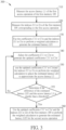
- FIG.3 illustrates a flowchart of a memory access latency estimation method 300 for the memory access latency estimation system 100 in FIG. 1 according to an embodiment.
- the memory access latency estimation method 300 may include the following steps.
- Step 310 to Step 355 the processor 130 may perform optimization to generate the updated coefficients C11' to C1n' to make the estimated access latency closer to the actual access latency.
- Step 355 may be omitted.
- the updated coefficients C11' to C1n' may be used to generate the estimated latency LE2 for the second access operation of the first memory 105 before the actual access latency is measured, and the estimated latency LE2 may be used to control the memory 105 and manage the power consumption.
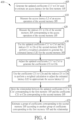
- FIG.4 illustrates a flowchart of a memory access latency estimation method 400 for the memory access latency estimation system 200 in FIG.2 according to another embodiment.
- the method 400 may include the following steps.
- Step 405 may include Step 310 to Step 355 of FIG.1 to generate and optimize the updated coefficients C1 1' to C1n' used to estimate the access latency of the first memory 105.
- Step 440 and Step 450 may be performed repeatedly to adjust the coefficients C21 to C2n until a difference of the generated estimated access latency (e.g. LE3) and the actual access latency L2 is smaller than a threshold.
- the neural network model in the processor 130 may be used to analyze and generate the relationship (e.g. the abovementioned function f()).
- the function e.g.
- the function f()) of the relationship may be generated according to a posterior probability and/or linear regression using a machine learning model and/or a neural network model of the processor 130.
- the relationship e.g. the function f()
- the relationship may be applied to find the group of coefficients corresponding to the second memory 205 for estimating the access latency for the second memory 205.
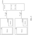
- FIG.5 illustrates a memory access latency estimation system 500 for controlling the first memory 105 and a second memory 205 according to another embodiment.
- the memory access latency estimation system 500 can include monitors 510, monitors 520 and a processor 570.
- FIG.6 is a flowchart of a memory access latency estimation method 600 for the memory access latency estimation system 500 in FIG.5 .
- the memory access latency estimation method 600 may include the following steps.
- the memory 105 can be embedded in a first chip, and the second memory 205 can be embedded in a second chip.
- the coefficients for estimating the latency of the first memory 105 in the first chip may be converted to the coefficients for estimating the latency of the second memory 205 in the second chip.
- a known formula can be used to calculate the access latency of the first memory 105.
- number and types of the indexes I11 to I1n can be fixed.
- the coefficients C11 to C1n, which are used to calculate the access latency of the first memory 105 have been optimized and are now fixed.
- This formula can be applied for a weighted calculation, for instance, the calculation like C11*I11+C12*I12+...+ C1n*I1n to generate the access latency of the first memory 105.
- the monitors 510 can measure the first memory 105 to generate the indexes I11 to I1n.
- the characteristics of the first memory 105 can be measured according to the indexes I11 to I1n.
- the monitors 520 can measure the second memory 205 to generate the indexes I21 to I2n.
- the characteristics of the second memory 205 can be measured according to the indexes I21 to I2n.
- the relationship can correspond to a mapping between the characteristics of the first memory 105 and the second memory 205.
- a neural network model in the processor 570 may be used to analyze and generate the relationship between the indexes I11 to I1n (of the first memory 105) and the indexes I21 to I2n (of the second memory 205).
- the relationship may be a function generated according to a posterior probability and/or linear regression using a machine learning model and/or a neural network model of the processor 570.
- the relationship in Step 630 can be expressed as a function and a formula.
- the number and the types of the indexes I11 to I1n can be the same as the number and types of the indexes I21 to I2n.
- Step 640 the coefficients C21 to C2n for the second memory 205 can be generated according to the known coefficients C11 to C1n of the first memory 105 and the relationship obtained in Step 630.
- the coefficients C21 to C2n can be used to estimate the access latency of the second memory 205.
- the coefficients C21 to C2n and a group of measured indexes I21' to I2n' of the second memory 205 can be used to perform a weighted calculation to estimate the access latency of the second memory 205.
- the estimated access latency of the second memory 205 can be generated with a formula such as C21 *I21' + C22*I22' + ... + C2n*I2n'.
- an access latency of an access operation of a memory may be estimated.
- the coefficients for estimating the access latency for the second memory 205 may be generated according known coefficients for the first memory 105.
- the coefficients for estimating the access latency of the second memory 205 can be generated according known coefficients for the first memory 105.
- the effort for calculating the coefficients for the second memory 205 is effectively reduced.
- an improved solution for estimating memory access latency is provided based on machine learning and neural network model, and it is helpful for power management to reduce the power consumption.
Landscapes
- Engineering & Computer Science (AREA)
- Theoretical Computer Science (AREA)
- Physics & Mathematics (AREA)
- General Engineering & Computer Science (AREA)
- General Physics & Mathematics (AREA)
- Human Computer Interaction (AREA)
- Debugging And Monitoring (AREA)
- Techniques For Improving Reliability Of Storages (AREA)
Applications Claiming Priority (2)
| Application Number | Priority Date | Filing Date | Title |
|---|---|---|---|
| US202363498029P | 2023-04-25 | 2023-04-25 | |
| US18/642,859 US20240361927A1 (en) | 2023-04-25 | 2024-04-23 | Memory access latency estimation method and memory access latency estimation system for estimating an access latency of a memory according to a plurality of coefficients and a plurality of indexes |
Publications (2)
| Publication Number | Publication Date |
|---|---|
| EP4456072A2 true EP4456072A2 (de) | 2024-10-30 |
| EP4456072A3 EP4456072A3 (de) | 2024-12-18 |
Family
ID=90880600
Family Applications (1)
| Application Number | Title | Priority Date | Filing Date |
|---|---|---|---|
| EP24172130.7A Pending EP4456072A3 (de) | 2023-04-25 | 2024-04-24 | Speicherzugrifflatenzschätzverfahren und speicherzugrifflatenzschätzsystem zur schätzung einer speicherzugrifflatenz nach mehreren koeffizienten und indizes |
Country Status (3)
| Country | Link |
|---|---|
| US (1) | US20240361927A1 (de) |
| EP (1) | EP4456072A3 (de) |
| TW (1) | TWI882781B (de) |
Family Cites Families (3)
| Publication number | Priority date | Publication date | Assignee | Title |
|---|---|---|---|---|
| TW201216163A (en) * | 2010-10-12 | 2012-04-16 | Ind Tech Res Inst | Memory modeling method and model generator |
| US11074011B2 (en) * | 2019-03-20 | 2021-07-27 | Western Digital Technologies, Inc. | Solid state drive latency estimation interface for host performance tuning |
| CN113505084B (zh) * | 2021-06-24 | 2023-09-12 | 中国科学院计算技术研究所 | 基于访存和性能建模的内存资源动态调控方法及系统 |
-
2024
- 2024-04-23 US US18/642,859 patent/US20240361927A1/en active Pending
- 2024-04-24 EP EP24172130.7A patent/EP4456072A3/de active Pending
- 2024-04-25 TW TW113115532A patent/TWI882781B/zh active
Also Published As
| Publication number | Publication date |
|---|---|
| TW202443403A (zh) | 2024-11-01 |
| TWI882781B (zh) | 2025-05-01 |
| EP4456072A3 (de) | 2024-12-18 |
| US20240361927A1 (en) | 2024-10-31 |
Similar Documents
| Publication | Publication Date | Title |
|---|---|---|
| KR102891516B1 (ko) | 전력 측정에 기초한 온도 검출 및 열 관리를 위한 방법 및 장치 | |
| WO2023202355A1 (zh) | 一种基于边界面塑性模型的土体状态数据计算方法及装置 | |
| US7480750B2 (en) | Optimization of buffer pool sizes for data storage | |
| CN119595992A (zh) | 基于卡尔曼滤波的测频方法、装置、电子设备及存储介质 | |
| CN118070040A (zh) | 一种炼钢厂数据采集方法、装置、电子设备及存储介质 | |
| US20240361927A1 (en) | Memory access latency estimation method and memory access latency estimation system for estimating an access latency of a memory according to a plurality of coefficients and a plurality of indexes | |
| US12254418B2 (en) | Systems and methods for heuristic algorithms with variable effort parameters | |
| US20250225390A1 (en) | Data processing method, data processing apparatus, and computer-readable storage medium | |
| CN112464599A (zh) | 应用在电路的静态时序分析中确定电源电压数据的方法 | |
| US10644968B1 (en) | Sampling in sliding windows with tight optimality and time decayed design | |
| TW202024925A (zh) | 卷積神經網路的特徵圖存取方法及其系統 | |
| CN118838706A (zh) | 内存访问延迟估算方法及根据多个系数和多个索引估算内存访问延迟的内存访问延迟估算系统 | |
| CN115841136A (zh) | 神经网络的量化方法、装置、芯片、板卡及设备 | |
| CN113762472A (zh) | 一种神经网络的指令序列生成方法及装置 | |
| JP6517706B2 (ja) | 効率的に数値制御データの受け渡しをする数値制御システム | |
| CN120104304A (zh) | 一种计算卸载与资源分配联合优化方法及装置 | |
| CN117667614B (zh) | 调节压测系统响应时长的方法、装置、设备、介质 | |
| CN114648456B (zh) | 超声图像的降噪方法和电子设备 | |
| CN112545484B (zh) | 医学成像系统校准时间确定方法、装置和计算机设备 | |
| JP7601236B2 (ja) | 情報処理装置および情報処理方法 | |
| US20230068381A1 (en) | Method and electronic device for quantizing dnn model | |
| JP2002328162A (ja) | 目標追尾装置 | |
| US20250383915A1 (en) | Non-transitory computer-readable recording medium, information processing apparatus, and information processing method | |
| CN113204411A (zh) | 一种数据处理方法、中间处理设备及存储介质 | |
| JP7563575B2 (ja) | 情報処理装置、情報処理方法およびプログラム |
Legal Events
| Date | Code | Title | Description |
|---|---|---|---|
| PUAI | Public reference made under article 153(3) epc to a published international application that has entered the european phase |
Free format text: ORIGINAL CODE: 0009012 |
|
| STAA | Information on the status of an ep patent application or granted ep patent |
Free format text: STATUS: THE APPLICATION HAS BEEN PUBLISHED |
|
| AK | Designated contracting states |
Kind code of ref document: A2 Designated state(s): AL AT BE BG CH CY CZ DE DK EE ES FI FR GB GR HR HU IE IS IT LI LT LU LV MC ME MK MT NL NO PL PT RO RS SE SI SK SM TR |
|
| PUAL | Search report despatched |
Free format text: ORIGINAL CODE: 0009013 |
|
| AK | Designated contracting states |
Kind code of ref document: A3 Designated state(s): AL AT BE BG CH CY CZ DE DK EE ES FI FR GB GR HR HU IE IS IT LI LT LU LV MC ME MK MT NL NO PL PT RO RS SE SI SK SM TR |
|
| RIC1 | Information provided on ipc code assigned before grant |
Ipc: G06F 13/16 20060101ALI20241112BHEP Ipc: G11C 29/02 20060101AFI20241112BHEP |
|
| STAA | Information on the status of an ep patent application or granted ep patent |
Free format text: STATUS: REQUEST FOR EXAMINATION WAS MADE |
|
| 17P | Request for examination filed |
Effective date: 20250220 |
|
| GRAP | Despatch of communication of intention to grant a patent |
Free format text: ORIGINAL CODE: EPIDOSNIGR1 |
|
| STAA | Information on the status of an ep patent application or granted ep patent |
Free format text: STATUS: GRANT OF PATENT IS INTENDED |