EP4455893A1 - Systeme, verfahren und vorrichtung für vorrichtungen mit speicher- und speicherkonfigurationen - Google Patents
Systeme, verfahren und vorrichtung für vorrichtungen mit speicher- und speicherkonfigurationen Download PDFInfo
- Publication number
- EP4455893A1 EP4455893A1 EP24166807.8A EP24166807A EP4455893A1 EP 4455893 A1 EP4455893 A1 EP 4455893A1 EP 24166807 A EP24166807 A EP 24166807A EP 4455893 A1 EP4455893 A1 EP 4455893A1
- Authority
- EP
- European Patent Office
- Prior art keywords
- memory
- storage
- media
- cache
- storage media
- Prior art date
- Legal status (The legal status is an assumption and is not a legal conclusion. Google has not performed a legal analysis and makes no representation as to the accuracy of the status listed.)
- Pending
Links
Images






Classifications
-
- G—PHYSICS
- G06—COMPUTING OR CALCULATING; COUNTING
- G06F—ELECTRIC DIGITAL DATA PROCESSING
- G06F12/00—Accessing, addressing or allocating within memory systems or architectures
- G06F12/02—Addressing or allocation; Relocation
- G06F12/08—Addressing or allocation; Relocation in hierarchically structured memory systems, e.g. virtual memory systems
- G06F12/0802—Addressing of a memory level in which the access to the desired data or data block requires associative addressing means, e.g. caches
- G06F12/0866—Addressing of a memory level in which the access to the desired data or data block requires associative addressing means, e.g. caches for peripheral storage systems, e.g. disk cache
- G06F12/0868—Data transfer between cache memory and other subsystems, e.g. storage devices or host systems
-
- G—PHYSICS
- G06—COMPUTING OR CALCULATING; COUNTING
- G06F—ELECTRIC DIGITAL DATA PROCESSING
- G06F3/00—Input arrangements for transferring data to be processed into a form capable of being handled by the computer; Output arrangements for transferring data from processing unit to output unit, e.g. interface arrangements
- G06F3/06—Digital input from, or digital output to, record carriers, e.g. RAID, emulated record carriers or networked record carriers
- G06F3/0601—Interfaces specially adapted for storage systems
- G06F3/0628—Interfaces specially adapted for storage systems making use of a particular technique
- G06F3/0655—Vertical data movement, i.e. input-output transfer; data movement between one or more hosts and one or more storage devices
- G06F3/0656—Data buffering arrangements
-
- G—PHYSICS
- G06—COMPUTING OR CALCULATING; COUNTING
- G06F—ELECTRIC DIGITAL DATA PROCESSING
- G06F3/00—Input arrangements for transferring data to be processed into a form capable of being handled by the computer; Output arrangements for transferring data from processing unit to output unit, e.g. interface arrangements
- G06F3/06—Digital input from, or digital output to, record carriers, e.g. RAID, emulated record carriers or networked record carriers
- G06F3/0601—Interfaces specially adapted for storage systems
- G06F3/0602—Interfaces specially adapted for storage systems specifically adapted to achieve a particular effect
- G06F3/0604—Improving or facilitating administration, e.g. storage management
-
- G—PHYSICS
- G06—COMPUTING OR CALCULATING; COUNTING
- G06F—ELECTRIC DIGITAL DATA PROCESSING
- G06F12/00—Accessing, addressing or allocating within memory systems or architectures
- G06F12/02—Addressing or allocation; Relocation
- G06F12/08—Addressing or allocation; Relocation in hierarchically structured memory systems, e.g. virtual memory systems
- G06F12/0802—Addressing of a memory level in which the access to the desired data or data block requires associative addressing means, e.g. caches
-
- G—PHYSICS
- G06—COMPUTING OR CALCULATING; COUNTING
- G06F—ELECTRIC DIGITAL DATA PROCESSING
- G06F13/00—Interconnection of, or transfer of information or other signals between, memories, input/output devices or central processing units
- G06F13/14—Handling requests for interconnection or transfer
-
- G—PHYSICS
- G06—COMPUTING OR CALCULATING; COUNTING
- G06F—ELECTRIC DIGITAL DATA PROCESSING
- G06F3/00—Input arrangements for transferring data to be processed into a form capable of being handled by the computer; Output arrangements for transferring data from processing unit to output unit, e.g. interface arrangements
- G06F3/06—Digital input from, or digital output to, record carriers, e.g. RAID, emulated record carriers or networked record carriers
- G06F3/0601—Interfaces specially adapted for storage systems
- G06F3/0628—Interfaces specially adapted for storage systems making use of a particular technique
- G06F3/0655—Vertical data movement, i.e. input-output transfer; data movement between one or more hosts and one or more storage devices
- G06F3/0658—Controller construction arrangements
-
- G—PHYSICS
- G06—COMPUTING OR CALCULATING; COUNTING
- G06F—ELECTRIC DIGITAL DATA PROCESSING
- G06F3/00—Input arrangements for transferring data to be processed into a form capable of being handled by the computer; Output arrangements for transferring data from processing unit to output unit, e.g. interface arrangements
- G06F3/06—Digital input from, or digital output to, record carriers, e.g. RAID, emulated record carriers or networked record carriers
- G06F3/0601—Interfaces specially adapted for storage systems
- G06F3/0628—Interfaces specially adapted for storage systems making use of a particular technique
- G06F3/0655—Vertical data movement, i.e. input-output transfer; data movement between one or more hosts and one or more storage devices
- G06F3/0659—Command handling arrangements, e.g. command buffers, queues, command scheduling
-
- G—PHYSICS
- G06—COMPUTING OR CALCULATING; COUNTING
- G06F—ELECTRIC DIGITAL DATA PROCESSING
- G06F3/00—Input arrangements for transferring data to be processed into a form capable of being handled by the computer; Output arrangements for transferring data from processing unit to output unit, e.g. interface arrangements
- G06F3/06—Digital input from, or digital output to, record carriers, e.g. RAID, emulated record carriers or networked record carriers
- G06F3/0601—Interfaces specially adapted for storage systems
- G06F3/0668—Interfaces specially adapted for storage systems adopting a particular infrastructure
- G06F3/0671—In-line storage system
- G06F3/0673—Single storage device
- G06F3/0679—Non-volatile semiconductor memory device, e.g. flash memory, one time programmable memory [OTP]
-
- G—PHYSICS
- G06—COMPUTING OR CALCULATING; COUNTING
- G06F—ELECTRIC DIGITAL DATA PROCESSING
- G06F2212/00—Indexing scheme relating to accessing, addressing or allocation within memory systems or architectures
- G06F2212/10—Providing a specific technical effect
- G06F2212/1016—Performance improvement
-
- G—PHYSICS
- G06—COMPUTING OR CALCULATING; COUNTING
- G06F—ELECTRIC DIGITAL DATA PROCESSING
- G06F2212/00—Indexing scheme relating to accessing, addressing or allocation within memory systems or architectures
- G06F2212/10—Providing a specific technical effect
- G06F2212/1016—Performance improvement
- G06F2212/1024—Latency reduction
Definitions
- This disclosure relates generally to devices with memory and storage, and more specifically to systems, methods, and apparatus for devices with memory and storage configurations.
- a storage device may include one or more storage media configured to store data received at the storage device.
- a storage device may communicate with a host, a storage system, and/or the like using a storage interface, a storage protocol, and/or the like.
- An application or other user may access storage media at a storage device using read and/or write commands.
- a device may include a cache media, a storage media, a communication interface, and at least one control circuit configured to receive, using the communication interface, a first memory access request to access a portion of the storage media, receive, using the communication interface, a second memory access request to access the portion of the storage media, access, based on the first memory access request, the portion of the storage media, and access, based on the second memory access request, a portion of the cache media.
- the portion of the cache media may include a first cache
- the at least one control circuit may be configured to access, based on the first memory access request, the portion of the storage media by reading data from the portion of the storage media, storing the data in a second cache, and loading at least a portion of the data from the second cache.
- the at least one control circuit may be configured to write at least a portion of the portion of the cache media to the portion of the storage media.
- the portion of the storage media may be a first portion of the storage media, and the at least one control circuit may be configured to receive, using the communication interface, a storage access request to access a second portion of the storage media, and access, based on the storage access request, the second portion of the storage media.
- the at least one control circuit may be configured to receive the first memory access request using a first protocol, and receive the storage access request using a second protocol.
- the at least one control circuit may be configured to operate the portion of the cache media and the first portion of the storage media as a first logical device, and operate the second portion of the storage media as a second logical device.
- the at least one control circuit may be configured to receive, using the communication interface, a storage access request to access the portion of the storage media, and access, based on the storage access request, the portion of the storage media.
- the at least one control circuit may be configured to receive the first memory access request using a first protocol, and receive the storage access request using a second protocol.
- the first protocol may include a memory access protocol
- the second protocol may include a storage access protocol.
- the at least one control circuit may be configured to perform a coherency operation associated with the portion of the storage media.
- the portion of the storage media may be a first portion of the storage media, and the at least one control circuit may be configured to write at least a portion of the portion of the cache media to a second portion of the storage media.
- the at least one control circuit may include work logic configured to receive a command, and perform, based on the command, a data movement operation or an operation associated with the portion of the cache media.
- a device may include a memory media, a storage media, a communication interface, and at least one control circuit configured to receive, using the communication interface, a memory access request to access a portion of the memory media, access, based on the memory access request, the portion of the storage media, and write the portion of the memory media to a portion of the storage media.
- the portion of the storage media may be a first portion of the storage media
- the at least one control circuit may be configured to receive, using the communication interface, a storage access request to access a second portion of the storage media, and access, based on the storage access request, the second portion of the storage media.
- the at least one control circuit may be configured to operate the portion of the memory media and the first portion of the storage media as a first logical device, and operate the second portion of the storage media as a second logical device.
- the portion of the memory media may be a first portion of the memory media, and the at least one control circuit may be configured to access, based on the storage access request, a second portion of the memory media.
- a device may include media comprising cache media and storage media, a communication interface, and at least one control circuit configured to receive, using the communication interface, a first memory access request, access, based on the first memory access request, a first portion of the media, receive, using the communication interface, a first storage access request, access, based on the first storage access request, a second portion of the media, receive, using the communication interface, a second memory access request, receive, using the communication interface, a second storage access request, access, based on the second memory access request, a third portion of the media, and access, based on the second storage access request, the third portion of the media.
- the first portion of the media may include a portion of the cache media, and the at least one control circuit may be configured to write data from the portion of the cache media to a portion of the storage media.
- the at least one control circuit may be configured to map the first portion of the media to the second portion of the media.
- the at least one control circuit may be configured to access, based on the first storage access request, a portion of the cache media.
- Computing systems may include memory media which may have relatively short access times, but relatively high costs and/or low capacities compared to storage media.
- an operating system may implement memory using storage media.
- an operating system may implement memory mapped files that may be located on storage devices but may appear as memory to an application or other user.
- memory mapped files may have relatively long access times and/or may involve operating system overhead.
- a storage device in accordance with example embodiments of the disclosure may include storage media that may be accessed as memory.
- the storage device may also include memory media that may be configured as a cache for the storage media.
- at least a portion of the storage media may be configured to appear as volatile memory.
- some embodiments may present a relatively large storage media as a volatile memory space that may be mapped, for example, as system memory.
- the memory media that may be configured as a cache for the storage media may reduce access times (e.g., latency) for the volatile memory space.
- the storage media may be configured to appear as persistent memory.
- some embodiments may present a relatively large storage media as a persistent memory space.
- the memory media that may be configured as a cache may be persisted (e.g., written), for example, to the storage media (e.g., based on a power loss event).
- the memory media that may be configured as a cache may reduce access times (e.g., latency) for the persistent memory space.
- At least a portion of the storage media may be configured to appear as either memory or storage.
- a storage device may implement a first access method in which at least a portion of the storage media may be accessed as storage space.
- the storage device may also implement a second access method in which a portion (e.g., the same portion) of the storage media may be accessed as memory space.
- the storage device may also include memory media that may be configured as a cache for the storage media. If accessed as memory space, the storage media may be configured to appear as volatile and/or persistent memory.
- the memory media that may be configured as a cache may be persisted, for example, to the storage media (e.g., based on a power loss event).
- first and second access methods (which may be referred to as multi-mode or dual mode operation) may enable a user to create, manage, use, and/or the like, any storage-as-memory configuration.
- a storage device in accordance with example embodiments of the disclosure may include memory media (e.g., volatile memory media) that may be configured to appear as persistent memory.
- the memory media may be persisted, for example, to storage media in the storage device (e.g., based on a power loss event).
- some embodiments may present a relatively large amount of volatile memory as persistent memory space.
- a storage device may implement multiple memory and/or storage spaces (e.g., a memory space and a storage space) in the same device. In some embodiments, different spaces may be implemented as different logical devices.
- a first portion of a storage media may be configured to appear as volatile memory in a first logical device.
- a second portion of the storage media may be configured to appear as storage space in a second logical device.
- a first portion of a storage media may be configured to appear as persistent memory in a first logical device.
- a second portion of the storage media may be configured to appear as storage space in a second logical device.
- a storage device may enable a user to configure memory media and/or storage media to implement any of the configurations described herein, and/or other configurations. Such embodiments may be referred to as composable devices and/or may be characterized as having composable memory, storage, and/or storage-as-memory.
- composable may refer to an aspect of a device, memory media, storage media, controller, and/or the like, that may be capable of being configured, e.g., by a user.
- a storage device may enable a user to configure one or more portions of storage media as memory space (e.g., volatile and/or persistent), as storage space, or a combination thereof.
- a storage device may enable a user to configure one or more portions of memory media as a cache for storage media, as a volatile and/or persistent memory space, and/or the like, or a combination thereof.
- a storage device may enable a user to configure one or more portions of storage media to be accessed as memory space or storage space, for example, using different access methods.
- a storage device may implement one or more commands for cache operations (e.g., prefetch, invalidate, write back, and/or the like), data movement (e.g., moving data between a host system memory and a memory space in the storage device), and/or the like.
- one or more commands implemented by the storage device may offload one or more operations (e.g., memory transfer operations) from a host or other user.
- This disclosure encompasses numerous aspects relating to devices with memory and storage configurations.
- the aspects disclosed herein may have independent utility and may be embodied individually, and not every embodiment may utilize every aspect. Moreover, the aspects may also be embodied in various combinations, some of which may amplify some benefits of the individual aspects in a synergistic manner.
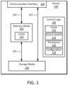
- Fig. 1 illustrates an embodiment of a device having memory and storage media in accordance with example embodiments of the disclosure.
- the device 100 illustrated in Fig. 1 may include memory media 102, storage media 104, one or more communication interfaces 106, and/or control logic 108.
- the communication interface 106 may be configured to enable a user to access the memory media 102 as shown by arrow 103 and/or the storage media 104 as shown by arrow 107.
- a portion (e.g., some or all) of the storage media 104 may be configured to appear as memory, for example, visible to (e.g., accessible by) a user through the communication interface 106.
- a portion of the memory media 102 may be configured as a cache 110 for a portion of the storage media 104.
- the control logic 108 may implement, facilitate, control, and/or the like, one or more schemes for the configuration, operation, and/or the like, of one or more components of the device 100.
- the control logic 108 may include various types of logic such as cache logic 112, access control logic 114, persistency logic 116, configuration logic 118, and/or the like. Not every embodiment of control logic 108 may include each type of logic, and some embodiments may include additional types of logic not illustrated in Fig. 1 . Any or all of the control logic 108 may be implemented as a single component (e.g., implemented with a single processor) or may be implemented with separate components, operations, and/or the like, for example, using separate processors, logic circuits, and/or the like).
- control logic 108 may include cache logic 112 that may configure and/or control the operation of the cache portion 110 of the memory media 102.
- cache control operations may include implementing one or more cache mappings, data writing policies (e.g., write-through, write-back, and/or the like), cache replacement policies, and/or the like.
- a cache may be used to improve one or more aspects (e.g., latency, power, and/or the like) of accessing data in an underlying medium.
- the cache logic 112 may configure the cache portion 110 of the memory media 102 to operate as a cache for a portion of the storage media 104.
- the control logic 108 may receive a storage access request to write user data in the portion of the storage media 104.
- the cache logic 112 may, based on the storage access request (e.g., a write request), store a copy of the user data in the cache portion 110 of the memory media 102.
- the cache logic 112 may also proceed (e.g., without delay) to write the user data to the portion of the storage media 104 as shown by arrow 105, e.g., if the cache logic 112 implements a write-through policy, or the cache logic 112 may wait until the user data is evicted from the cache portion 110 of the memory media 102 to write the user data to the portion of the storage media 104 as shown by arrow 105, e.g., if the cache logic 112 implements a write-back policy.
- the cache logic 112 may implement a cache policy (e.g., a predictive policy, eviction policy, and/or the like) in which the cache logic 112 may copy user data from storage media 104 to the cache portion 110 of the memory media 102 in anticipation of the user data being accessed by a user.
- the cache logic 112 may evict other user data from the cache portion 110 of the memory media 102 to make room for the user data being copied from the storage media 104.
- the cache logic 112 may service the storage access request (e.g., a read request) by loading the user data from the cache portion 110 of the memory media 102 as shown by arrow 103 instead of reading the user data from the portion of the storage media 104.
- the cache portion 110 of the memory media 102 may be implemented with memory media 102 that may have lower access latency than the portion of the storage media 104.
- the use of a cache may reduce the latency associated with accessing data from the underlying media.
- the use of a cache may reduce the amount of power consumption associated with performing an access operation to access data from the underlying media (e.g., a page read) because the data may already be available in the cache portion 110 of the memory media 102.
- control logic 108 may include access control logic 114 that may configure and/or control the operation of the memory media 102 and/or storage media 104 (or one or more portions thereof) to be visible or invisible to a user, to be accessible as memory, as storage, or a combination thereof, and/or the like.
- the access control logic 114 may operate to cause a portion of the storage media 104 (which may have a native block-based interface scheme) to appear as visible memory (e.g., volatile memory and/or persistent memory).
- the access control logic 114 may read, from the storage media 104, a page in which the requested byte may be located. The access control logic 114 may obtain the requested byte from the page and return the requested byte in response to the load command (e.g., again using the memory access protocol through the communication interface 106).
- a memory access interface and/or protocol may access data in units of cache lines (e.g., 64 bytes), and thus, the access control logic 114 may return a requested cache line of data from the page read from the storage media 104.
- the access control logic 114 may configure and/or control the operation of the memory media 102 to be accessible as visible memory (e.g., using a memory access protocol through the communication interface 106).
- the access control logic 114 may implement a dual mode access scheme in which a portion of the storage media 104 may be accessed as either memory or storage.
- control logic 108 may include persistency logic 116 that may configure and/or control the operation of a portion of the memory media 102 to be persisted (e.g., copied to nonvolatile memory), for example, to the storage media 104 (e.g., based on a power loss event).
- persistency logic 116 may flush (e.g., copy) the contents of the cache 110 to the storage media 104 in response to a power loss event.
- Example embodiments of a persistent memory space that may be implemented with an invisible cache in memory media for a visible memory space in storage media are described below with respect to Figs. 4 and 5 .
- control logic 108 may include configuration logic 118 that may enable a user to configure one or more of the components, operations, and/or the like of the device 100.
- the configuration logic 118 may receive commands, instructions, and/or the like from a user (e.g., through the communication interface 106) that may enable a user to specify a size of the cache 110, whether the cache 110 operates as volatile memory and/or persistent memory, how much of the storage media 104 may be accessible as memory, how much of the storage media 104 may be accessible as storage, how much of the storage media 104 may be used to persist (e.g., store in nonvolatile media) some or all of the cache 110, and/or the like.
- a medium may be referred to as being configured as a cache, configured as visible, configured as invisible, and/or the like
- one or more controllers may actually be configured to use the medium in a manner that may cause the medium to appear as cache, appear as visible, appear as invisible, and/or the like.
- a reference to a medium configured in a certain manner may refer to an arrangement in which a controller (e.g., control logic) may be configured to cause the medium to operate as though it is configured in the certain manner.
- a portion of storage media 104 may be configured as visible memory that may be accessible to a user (e.g., in units of 64-byte cache lines using a memory access protocol through the communication interface 106), the user may not directly access the portion of the storage media 104. Instead, the control logic 108 may act as an intermediary to access, on behalf of the user, the portion of the storage media 104 (e.g., in units of pages and/or blocks using an underlying page and/or block-based interface, e.g., using a flash translation layer (FLT) in a solid state drive (SSD)).
- FLT flash translation layer
- SSD solid state drive
- control logic 108 may translate one or more access requests of a first type to one or more access requests of a second type.
- memory load and/or store requests which may usually be used to access memory media may be translated to and/or from storage read and/or write requests which may usually be used to access storage media.
- one or more underlying caches may be used to implement one or more translations.
- the control logic 108 may receive, from a user, a memory access request to load a cache line of data (e.g., a 64-bit cache line) from the portion of the storage media 104 configured as visible memory.
- a cache line of data e.g., a 64-bit cache line
- the storage media may only be accessible in units of 4K byte pages.
- control logic 108 may translate the memory access request to a storage read request that may read a page containing the requested cache line from the storage media 104 and store it in a cache that may be hidden from the user. The control logic 108 may then load the requested cache line of data from the hidden cache and return it to the user in response to the memory access request.
- Fig. 1 may be used, for example, to implement devices having various configurations of memory media and/or storage media which may be referred to as modes of operation. Depending on the implementation details, some embodiments may present a relatively large storage media as a volatile memory space, a persistent memory space, a storage space, or a combination thereof.
- the arrows 103, 105, and/or 107 shown in Fig. 1 may illustrate data flow that, depending on the implementation details, may show end-to-end data flow and to simplify the drawing may not illustrate one or more intermediate components such as memory device interfaces, storage device interfaces, translation apparatus (e.g., a flash translation layer (FTL)), buffers, controllers, and/or the like, through which the data may flow.
- translation apparatus e.g., a flash translation layer (FTL)
- FTL flash translation layer
- buffers e.g., a flash translation layer (FTL)
- controllers e.g., a flash translation layer
- NVMe controller e.g., an NVMe controller as
- control logic 108 data that may be transferred between the communication interface 106 and memory media 102 (e.g., using a CXL protocol) as shown by arrow 103 may pass through a memory protocol controller (e.g., a CXL interface controller as illustrated in Figs. 5-9 ) in control logic 108.
- a memory protocol controller e.g., a CXL interface controller as illustrated in Figs. 5-9
- data that may be transferred between the memory media 102 and the storage media 104 as shown by arrow 105 may pass through a memory protocol controller (e.g., a CXL interface controller) and/or a storage protocol controller (e.g., an NVMe controller) in control logic 108.
- a memory protocol controller e.g., a CXL interface controller
- a storage protocol controller e.g., an NVMe controller
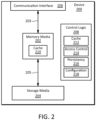
- Fig. 2 illustrates another embodiment of a device having memory and storage media in accordance with example embodiments of the disclosure.
- the device 200 illustrated in Fig. 2 may include one or more elements similar to the embodiment illustrated in Fig. 1 in which similar elements may be indicated by reference numbers ending in, and/or containing, the same digits, letters, and/or the like.
- the device 200 may include memory media 202, storage media 204, a communication interface 206, and/or control logic 208 that may operate in a manner similar to corresponding components in Fig 1 .
- the access control logic 214 may configure and/or control the memory media 202 to appear as persistent memory that may be visible to (e.g., accessible by) a user through the communication interface 206.
- the persistency logic 216 may configure and/or control the memory media 202 to be persisted, for example, to the storage media 204 (e.g., based on a power loss event).
- the access control logic 214 may essentially implement an entire visible persistent memory space with a portion of the memory media 202 that may be persisted to the storage media 204. Depending on the implementation details, this may result in a relatively high-performance (e.g., low latency) persistent memory space because, for example, essentially all access requests for the persistent memory space may be serviced by the memory media 202 rather than involving an access of the storage media 204.
- Example embodiments of a persistent memory space that may be implemented with a visible memory space in memory media with an invisible persistence space in storage media are described below with respect to Figs. 6 and 7 .
- Fig. 2 may be used, for example, to implement devices having various configurations of memory media and/or storage media which may be referred to as modes of operation.
- the arrows 203 and/or 205 shown in Fig. 2 may illustrate data flow that, depending on the implementation details, may show end-to-end data flow and to simplify the drawing may not illustrate one or more intermediate components such as memory device interfaces, storage device interfaces, translation apparatus (e.g., a flash translation layer (FTL)), buffers, controllers, and/or the like, through which the data may flow.
- translation apparatus e.g., a flash translation layer (FTL)
- FTL flash translation layer
- data that may be transferred between the communication interface 206 and memory media 202 (e.g., using a CXL protocol) as shown by arrow 203 may pass through a memory protocol controller (e.g., a CXL interface controller) in control logic 208.
- a memory protocol controller e.g., a CXL interface controller
- data that may be transferred between the memory media 202 and the storage media 204 as shown by arrow 205 may pass through a memory protocol controller (e.g., a CXL interface controller) and/or a storage protocol controller (e.g., an NVMe controller) in control logic 208.
- a memory protocol controller e.g., a CXL interface controller
- a storage protocol controller e.g., an NVMe controller
- memory media may be implemented with volatile memory media such as dynamic random access memory (DRAM), static random access memory (SRAM), and/or the like
- storage media may be implemented with nonvolatile memory media such as magnetic media, solid state nonvolatile memory media (e.g., flash memory which may include not-AND (NAND) flash memory, NOR flash memory, cross-gridded nonvolatile memory, memory with bulk resistance change, phase change memory (PCM), and/or the like), optical media, and/or the like.
- nonvolatile memory media such as magnetic media, solid state nonvolatile memory media (e.g., flash memory which may include not-AND (NAND) flash memory, NOR flash memory, cross-gridded nonvolatile memory, memory with bulk resistance change, phase change memory (PCM), and/or the like), optical media, and/or the like.
- NAND not-AND
- NOR flash memory NOR flash memory
- PCM phase change memory
- memory media may be addressable in relatively smaller units such as bytes, words, cache lines, and/or the like, whereas storage media may be addressable in relatively larger units such as pages, blocks, sectors, and/or the like.
- memory media may be accessed by software using load and/or store instructions, whereas storage media may be accessed by software using read and/or write instructions.
- memory media may be accessed using a memory interface and/or protocol such as double data rate (DDR) of any generation (e.g., DDR4, DDR5, etc.), direct memory access (DMA), remote DMA (RDMA), Open Memory Interface (OMI), Compute Express Link (CXL), Gen-Z, and/or the like
- DDR double data rate
- DMA direct memory access
- RDMA remote DMA
- OMI Open Memory Interface
- CXL Compute Express Link
- Gen-Z Gen-Z
- storage media may be accessed using a storage interface and/or protocol such as serial ATA (SATA), Small Computer System Interface (SCSI), serial attached SCSI (SAS), Nonvolatile Memory Express (NVMe), NVMe over fabrics (NVMe-oF), and/or the like.
- SATA serial ATA
- SCSI Small Computer System Interface
- SAS serial attached SCSI
- NVMe Nonvolatile Memory Express
- NVMe-oF NVMe over fabrics
- a memory interface and/or protocol may access data in relatively smaller units such as bytes, words, cache lines, and/or the like, whereas a storage interface and/or protocol may access data in relatively larger units such as pages, blocks, sectors, and/or the like.
- any of the devices 100 and/or 200 as well as any other devices disclosed herein may be implemented in any form such as storage devices, accelerators, network interface cards and/or network interface controllers (NICs), and/or the like, having any physical form factor including one or more form factors used for storage devices (e.g., solid state drives (SSDs), hard disk drives (HDDs), optical drives, and/or the like) such as Peripheral Component Interconnect Express (PCIe) add-in cards, 3.5 inch drives, 2.5 inch drives, 1.8 inch drives, M.2 drives, U.2 and/or U.3 drives, Enterprise and Data Center SSD Form Factor (EDSFF) drives, any of the SFF-TA-100X form factors (e.g., SFF-TA-1002), NF1, and/or the like, using any connector configuration such as SATA, SCSI, SAS, M.2, U.2, U.3 and/or the like.
- a device may be implemented in any other form, for example, as a collection of one or more components
- cache media may be implemented with memory media such as DRAM
- other types of media e.g., storage media
- cache media may be used for cache media.
- some or all of the caches 110 and/or 210 may be implemented with media other than memory media that may have one or more relative characteristics (e.g., relative to a storage media 104 and/or 204) that may make one or both of them more suitable for their respective functions.
- the storage media 104 and/or 204 may be implemented with magnetic media which may have a relatively higher capacity, lower cost, and/or the like, whereas some or all of the caches 110 and/or 210 may be implemented with NAND flash which may have relatively lower access latency that may make it relatively more suitable for use as a cache.
- any of the devices 100 and/or 200 as well as any other devices disclosed herein may be used in connection with one or more personal computers, smart phones, tablet computers, servers, server chassis, server racks, datarooms, datacenters, edge datacenters, mobile edge datacenters, and/or any combinations thereof.
- any of the communication interfaces 106 and/or 206 as well as any other communication interfaces disclosed herein may be implemented with any interconnect interface and/or protocol such as PCIe, NVMe, NVMe Key-Value (NVMe-KV), SATA, SAS, SCSI, Compute Express Link (CXL) and/or a one or more CXL protocols such as CXL.mem, CXL.cache, and/or CXL.io, Gen-Z, Coherent Accelerator Processor Interface (CAPI), Cache Coherent Interconnect for Accelerators (CCIX), and/or the like, or any combination thereof.
- PCIe Peripherent Memory Express Interface
- NVMe-KV NVMe Key-Value
- SATA Serial Advanced Technology Attachment
- SAS Serial Bus Component Interconnect
- CXL Compute Express Link
- CXL protocols such as CXL.mem, CXL.cache, and/or CXL.io, Gen-Z, Coher
- any of the communication interfaces 106 and/or 206 as well as any other communication interfaces disclosed herein may be implemented with any networking interface and/or protocol such as Ethernet, Transmission Control Protocol/Internet Protocol (TCP/IP), remote direct memory access (RDMA), RDMA over Converged Ethernet (RoCE), Fibre Channel, InfiniBand (IB), iWARP, NVMe-over-fabrics (NVMe-oF), and/or the like, or any combination thereof.
- TCP/IP Transmission Control Protocol/Internet Protocol
- RDMA remote direct memory access
- RoCE RDMA over Converged Ethernet
- Fibre Channel Fibre Channel
- IB InfiniBand
- IB InfiniBand
- iWARP NVMe-over-fabrics
- NVMe-oF NVMe-over-fabrics
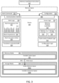
- Fig. 3 illustrates a first example embodiment of a scheme for configuring and/or operating a device having memory media and storage media in accordance with example embodiments of the disclosure.
- the embodiment illustrated in Fig. 3 may be used to implement, and/or may be implemented with, for example, the device illustrated in Fig. 1 in which similar elements may be indicated by reference numbers ending in, and/or containing, the same digits, letters, and/or the like.
- a device 300 may include memory media 302 that, in this example, may be implemented with DRAM but in other embodiments may be implemented with other types of memory media (e.g., volatile media that may have relatively high access speeds, e.g., relatively low latency).
- the device 300 may also include storage media 304 that, in this example, may be implemented with NAND flash but in other embodiments may be implemented with other types of storage media (e.g., nonvolatile media that may have relatively high capacity and/or relatively low cost).
- the device 300 may also include a communication interface 306 which, in this example, may implement one or more CXL protocols but in other embodiments may implement, or be implemented with, any other interfaces, protocols, and/or the like that may enable a user to access data as memory (e.g., DDR, OMI, Gen-Z, DMA, RDMA, and/or the like).
- the CXL (or other) protocol(s) may operate with any underlying transport scheme (e.g., physical layer, transport layer, and/or the like) including, for example, PCIe, Ethernet, InfiniBand, and/or the like.
- the device 300 may also include cache and/or prefetch logic 312 that may configure and/or control the operation of a cache portion 310 of the memory media 302.
- cache control operations may include implementing one or more cache mappings, data writing policies (e.g., write-through, write-back, and/or the like), cache replacement policies, and/or the like.
- the device 300 may also include access control logic 314 that may be implemented, at least in part, with a memory protocol controller 320 that, in this embodiment, may implement CXL (e.g., as a CXL interface controller), but in other embodiments may be implemented with any other type of protocol controller that may enable a user to access data as memory.
- the access control logic 314 may include a memory 324 controller which, in this example, may be implemented with a DRAM controller that may control DRAM that may be used to implement the memory media 302.
- the access control logic 314 may also include a storage controller 326 which, in this example, may be implemented with a flash translation layer (FTL) and/or a NAND controller (e.g.
- FTL flash translation layer
- NAND controller e.g.
- NAND channel controller that may control NAND flash that may be used to implement the storage media 304.
- access control logic 314 may include any of the memory and/or storage media access schemes disclosed herein including those described and illustrated with respect to Figs. 1 through 11 .
- the device 300 may also include configuration logic 318 that may enable a user to configure one or more of the components and/or operations illustrated in Fig. 3 , for example, based on configuration information 319.
- the configuration information 319 may be received from a user, for example, using the CXL.io protocol.
- Examples of configuration information 319 may include amounts, types, and/or the like of memory media 302, storage media 304, invisible cache space 310, visible memory space 304A, and/or invisible endurance space 304B, one or more cache policies, and/or the like that the configuration logic 318 may use to configure the media and/or spaces illustrated in Fig. 3 .
- the device 300 may also include a device translation lookaside buffer (TLB) 328 that may cache address translations, for example, to enable the device 300 to support shared virtual memory (SVM) by processing (e.g., directly) data from an application address space.
- TLB device translation lookaside buffer
- the device 300 may also include work logic 330 that may enable the device 300 to implement one or more operations related to data movement, cache management, memory management, storage management, and/or the like. Examples of operations that may be implemented by the work logic 330 may include artificial intelligence (AI) and/or machine learning (ML) training, inferencing, classification, generation, and/or the like.
- the work logic 330 may include a work acceptance unit 332 (which may also be referred to as a work submission unit), one or more work dispatchers 334, and/or one or more work execution units 336.
- the work acceptance unit 332 may include one or more work queues 333 (which may also be referred to as submission queues) that may accept commands to invoke any of the operations implemented by the work logic 330.
- the work execution unit may execute, based on the commands received at the work acceptance unit 332, any of the operations implemented by the work logic 330.
- the work dispatcher(s) 334 may fetch entries from the work queue(s) 333 and pass the entries to the work execution unit(s) 336 for execution.
- the work dispatcher(s) 334 may determine an order of execution of the commands based on various factors such as the availability, capacity, capability, and/or the like of one or more work execution units 336, the type of command and/or operation, one or more priorities, privileges, and/or the like.
- Examples of commands and/or operations related to data movement may include moving data to and/or from visible (which may also be referred to as exposed to and/or accessible by a user) memory, storage, and/or the like (e.g., moving data between a host system memory and a visible memory space in the storage device), prefetching data from a storage medium 304 to a cache 310, and/or the like.
- the work execution unit(s) 336 may perform data transfer operations using, for example, DMA, RDMA, RoCE, and/or the like.
- Examples of commands and/or operations related to cache management may include prefetching and/or invalidating data for writing back data (e.g., to storage medium 304) and/or discarding a portion of data in a cache 310.
- Examples of commands and/or operations related to storage management may include invalidating data, for example, to inform the storage controller 326 that data in the storage medium 304 may be invalid and therefore may be deleted and/or garbage collected from the storage medium 304.
- one or more commands and/or operations implemented by the work logic 330 may be offloaded from a host and/or other user.
- the work logic 330 may provide relatively efficient and/or low-overhead scheme for moving data in user mode, kernel-mode, and/or the like.
- some embodiments may implement one or more commands and/or operations similar to the work logic 330 using, for example, a relatively simple mechanism such as implementing commands using one or more CXL.io mechanisms (e.g., vendor-defined CXL.io mechanisms).
- a relatively simple mechanism such as implementing commands using one or more CXL.io mechanisms (e.g., vendor-defined CXL.io mechanisms).
- access logic 314, cache and/or prefetch logic 312, configuration logic 318, work logic 330, translation lookaside buffer 328, and/or the like may be characterized and/or referred to, collectively and/or individually, as control logic.
- a portion of the storage media 304 may be configured as a visible memory space 304A that may be exposed to a user as a memory space 303 (e.g., a volatile memory space).
- a portion of the memory media 302 may be configured as an invisible (to the user) cache space 310 for the visible memory space 304A.
- the cache space 310 may be used, for example, to reduce access times for frequency used data (which may be placed in the cache space 310 by cache and/or prefetch logic 312) and/or data that may be prefetched to the cache space 310 (e.g., by cache and/or prefetch logic 312, for example, based on receiving a prefetch work command 335 from a user).
- a user may access the memory space 303 using one or more memory load and/or store (load/store) instructions 307 that may be sent to the access logic 314 through the communication interface 306 using, for example, the CXL.mem protocol.
- load/store memory load and/or store instructions 307 that may be sent to the access logic 314 through the communication interface 306 using, for example, the CXL.mem protocol.
- the cache and/or prefetch logic 312 may use the memory controller 324 to load or store the data to or from the cache space 310.
- the cache and/or prefetch logic 312 may, depending on a cache replacement and/or eviction policy, store the new version of the data in the invisible cache space 310 and/or the visible memory space 304A. For instance, if the cache and/or prefetch logic 312 implements a least recently used (LRU) eviction policy, the cache and/or prefetch logic 312 may store the new data in the cache space 310 (e.g., because recently used data may be likely to be accessed again soon).
- LRU least recently used
- the cache and/or prefetch logic 312 may also store a copy of the new data in the visible memory space 304A in storage media 304 without delay if the cache and/or prefetch logic 312 implements a write-through policy, or the cache and/or prefetch logic 312 may store a copy of the new data in the visible memory space 304A in storage media 304 at a later time, (e.g., when the new data is later evicted) if the cache and/or prefetch logic 312 implements a write-back policy (e.g., an opportunistic write-back).
- a write-back policy e.g., an opportunistic write-back
- the cache and/or prefetch logic 312 may not store the new data in the cache space 310 in memory media 302 (e.g., because recently used data may not be likely to be accessed again for a relatively long time). Instead, the cache and/or prefetch logic 312 may store the new data in the visible memory space 304A in storage media 304.
- MRU most recently used
- the cache and/or prefetch logic 312 may load the requested data from the cache space 310.
- the access logic 314 may use the storage controller 326 to read or write the data from or to the visible memory space 304A.
- the access logic 314 and/or the storage controller 326 may access a page, block, sector, and/or the like, containing the requested data from the visible memory space 304A and extract or insert the requested data which may be a byte, word, cache line, and/or the like. If the access is a store, the access logic 314 and/or the storage controller 326 may write the modified page, block, sector, and/or the like, back to the visible memory space 304A.
- a copy of the accessed data may also be stored in the cache space 310.
- the access logic 314 and/or the storage controller 326 may return (e.g., send to the user that sent the request) the requested data which may be a byte, word, cache line, and/or the like.
- the access logic 314 and/or the storage controller 326 may store (e.g., temporarily) the page, block, sector, and/or the like, containing the requested data in a second cache after reading it from the visible memory space 304A in the storage media 304.
- the access logic 314 and/or the storage controller 326 may then extract the requested data from the second cache.
- the second cache may be implemented, for example, as part of the invisible cache space 310, within the access logic 314, and/or the like.
- a portion of the storage media 304 may be configured as invisible (to a user) endurance space (e.g., an overprovisioning (OP) space) 304B, for example, to enhance the endurance of the portion of the storage media 304 implemented as the visible memory space 304A.
- the invisible endurance space 304B may be implemented with a relatively large amount of storage media to compensate for a relatively large number of write cycles that may be encountered with a visible memory space 304A exposed as memory.
- the embodiment illustrated in Fig. 3 may expose a relatively large amount of storage media 304 as a volatile memory space 303 at a relatively low cost. Moreover, the portion of memory media 302 configured as cache space 310 may reduce access times (e.g., latency) for the memory space 303.
- the visible memory space 304A and invisible endurance space 304B may each be implemented with 1TB of storage media
- the memory space 303 may be implemented as a 1TB memory space
- the invisible cache space 310 may be implemented as a 16GB cache space.
- the memory space 303 may be suitable to be mapped as system memory (e.g., memory for general use that may be allocated using operating system (e.g., Linux) memory allocation commands such as malloc).
- system memory e.g., memory for general use that may be allocated using operating system (e.g., Linux) memory allocation commands such as malloc).
- a user such as an application may use the memory space 303 implemented in the embodiment illustrated in Fig. 3 without any awareness of, and/or capability of manipulating, the underlying configuration of memory media 302 and/or storage media 304.
- a host may run an operating system, virtual machine manager, and/or the like that may configure the memory space 303 and allocate memory from the memory space 303 to an application, virtual machine, and/or the like running on the host.
- the application, virtual machine, and/or the like may use the allocated memory from the memory space 303 without any awareness that the allocated memory may be implemented with storage media 304 and/or cache space 310 in memory media 302.
- a user e.g., a host, an application, a process, a service, an operating system, another device, and/or the like
- a user may use one or more features to enhance the performance, endurance, and/or the like of the device illustrated in Fig. 3 .
- the user may send a prefetch request to the cache and/or prefetch logic 312 (e.g., by submitting a work command 335 to the work acceptance unit 332) to cause the cache and/or prefetch logic 312 to store a copy of the data in the cache space 310.
- a prefetch request to the cache and/or prefetch logic 312 (e.g., by submitting a work command 335 to the work acceptance unit 332) to cause the cache and/or prefetch logic 312 to store a copy of the data in the cache space 310.
- the user may send a cache invalidate request to the cache and/or prefetch logic 312 (e.g., by submitting a work command 335 to the work acceptance unit 332) to cause the cache and/or prefetch logic 312 to invalidate the data in the cache space 310 and/or a corresponding location in the visible memory space 304.
- this may enable the storage controller 326 to garbage collect the data in the storage media 304.
- the user may send a data transfer request to transfer the data from the system memory to the memory space 303 (e.g., by submitting a work command 335 to the work acceptance unit 332).
- the work dispatcher(s) 334 may schedule the data transfer request to be executed, for example, by a work execution unit that may transfer the data, for example, using an RDMA operation.
- one or more of the features to enhance the performance, endurance, and/or the like may be used by middleware at a host or other user.
- Fig. 4 illustrates a second example embodiment of a scheme for configuring and/or operating a device having memory media and storage media in accordance with example embodiments of the disclosure.
- the embodiment illustrated in Fig. 4 may be used to implement, and/or may be implemented with, for example, the device illustrated in Fig. 1 in which similar elements may be indicated by reference numbers ending in, and/or containing, the same digits, letters, and/or the like.
- the device 400 illustrated in Fig. 4 may include one or more elements similar to the embodiment illustrated in Fig. 3 in which similar elements may be indicated by reference numbers ending in, and/or containing, the same digits, letters, and/or the like.
- the configuration and/or operation of the device 400 illustrated in Fig. 4 may be similar to the configuration and/or operation of the device 300 illustrated in Fig. 3 .
- at least a portion of the memory space 403 exposed to a user may be implemented as a persistent memory space.
- the persistent memory space 403 may be implemented with visible memory space 404A in storage media 404 which may be inherently persistent.
- the persistent memory space 403 may also be implemented with an invisible cache space 410 within memory media 402 that may be configured as a cache for the visible memory space 404A in storage media 404.
- the device 400 may configure a portion of the storage media 404 as an invisible persistence space 404C.
- the device 400 may also include persistency logic 416 and/or a persistency power source 417. In response to a power loss event, the persistency logic 416 may perform a data transfer operation to flush the contents of the invisible cache space 410 to the invisible persistence space 404C.
- the persistency power source 417 may be configured to provide power to one or more portions of the persistency logic 416, the memory media 402, the storage media 404, and/or any other components that may be involved in flushing data from the invisible cache space 410 to the invisible persistence space 404C.
- the persistency power source 417 may be implemented with one or more capacitors (e.g., supercapacitors), internal and/or external batteries, and/or the like.
- the persistency logic 416 may be implemented with or as a Global Persistency Flush (GPF) unit, for example, as part of CXL.
- GPF Global Persistency Flush
- access logic 414 cache and/or prefetch logic 412, configuration logic 418, work logic 430, translation lookaside buffer 428, persistency logic 416, and/or the like, may be characterized and/or referred to, collectively and/or individually, as control logic.
- the embodiment illustrated in Fig. 4 may expose a relatively large amount of storage media 404 as a persistent memory space 403 at a relatively low cost. Moreover, the portion of memory media 402 configured as cache space 410 may reduce access times (e.g., latency) for the persistent memory space 403. As with the embodiment illustrated in Fig. 3 , the access logic 414 in the device 400 may enable a user to access the visible memory space 404A in storage media 404 as memory, for example, using CXL.mem through the communication interface 406.
- the persistent memory space 403 may be implemented as special-purpose memory (which may also be referred to as protected memory or restricted memory). For example, if the device 400 is accessed using an operating system such as Linux, some or all of the persistent memory space 403 may be mapped as special-purpose memory which, depending on the implementation details, may prevent it from being allocated as system (e.g., general) memory using memory allocation commands such as malloc.
- special-purpose memory which may also be referred to as protected memory or restricted memory.
- the visible memory space 404A may be implemented with 1TB of storage media
- the persistent memory space 403 may be implemented as a 1TB memory space
- the invisible endurance space 404B may be implemented with 894GB of storage media
- the invisible cache space 410 may be implemented 16GB of memory media 402.
- Fig. 5 illustrates a third example embodiment of a scheme for configuring and/or operating a device having memory media and storage media in accordance with example embodiments of the disclosure.
- the embodiment illustrated in Fig. 5 may be used to implement, and/or may be implemented with, for example, the device illustrated in Fig. 1 in which similar elements may be indicated by reference numbers ending in, and/or containing, the same digits, letters, and/or the like.
- the device 500 illustrated in Fig. 5 may include one or more elements similar to the embodiments illustrated in Fig. 3 and/or Fig. 4 in which similar elements may be indicated by reference numbers ending in, and/or containing, the same digits, letters, and/or the like.
- the configuration and/or operation of the device 500 illustrated in Fig. 5 may be similar to the configuration and/or operation of the device 400 illustrated in Fig. 4 .
- a first portion of the storage media 504 may be configured as visible memory space 504A
- a second portion of the storage media 504 may be configured as visible storage space 504B.
- portions of the storage media 504 may be exposed as both persistent memory space 503 and storage space 505.
- a first portion of the memory media 502 may be configured as invisible cache space 510A for the visible memory space 504A (which may be exposed as persistent memory space 503).
- the visible storage space 504B may be operated without a cache, in some embodiments, a second portion of the memory media 502 may be configured as invisible read cache space 510B for the visible storage space 504B.
- a portion 504D of the storage media 504 may be configured as invisible persistence space for the invisible cache space 510A. Additionally, or alternatively, the portion 504D of the storage media 504 may be configured as invisible endurance space for the visible memory space 504A. In some embodiments, a portion of the storage media 504 may be configured as invisible endurance space 504C for the visible storage space 504B.
- the access logic 514 may include a storage protocol controller 521 that, in this embodiment, may be implemented with an NVMe controller, but in other embodiments may be implemented with any other type of protocol controller that may enable a user to access data as storage, for example, using logical block addresses (LBAs).
- an NVMe protocol may be implemented with an underlying transport scheme based on CXL.io.
- a user may access the storage space 505 using one or more storage read and/or write (read/write) instructions 509 that may be sent to the access logic 514 through the communication interface 506 using, for example, a storage protocol (which may also be referred to as a storage access protocol) such as NVMe (e.g., NVMe, NVMe-oF, and/or the like).
- a storage protocol which may also be referred to as a storage access protocol
- NVMe e.g., NVMe, NVMe-oF, and/or the like.
- the corresponding memory location in the visible storage space 504B in the storage media 504 may be updated using a write back operation 569 (e.g., opportunistic write back), a write through operation, and/or the like, which may be controlled, for example, by the cache and/or prefetch logic 512.
- a write back operation 569 e.g., opportunistic write back
- a write through operation e.g., a write through operation, and/or the like
- the access logic 514 may use the storage controller 526 to read or write the data from or to the visible storage space 504B. If the access is a write, the access logic 514 and/or the storage controller 526 may write the data (e.g., page, block, sector, and/or the like) to the visible storage space 504B. Depending on a cache replacement policy implemented by the cache and/or prefetch logic 512, a copy of the accessed data may be stored in the cache space 510B.
- the device 500 may expose a memory space 503 (which may be accessed using a memory access protocol such as CXL) and a storage space 505 (which may be accessed using a storage access protocol such as NVMe), both of which may be implemented with storage media 504.
- a memory space 503 which may be accessed using a memory access protocol such as CXL
- a storage space 505 which may be accessed using a storage access protocol such as NVMe
- Either or both of the memory space 503 and/or storage space 505 may also implement a cache (e.g., cache space 510A for memory space 503 and/or cache space 510B for storage space 505.
- the memory space 503 and storage space 505 may be implemented using separate logical devices.
- the memory protocol controller 520 may be implemented with a CXL interface controller as a first logical device
- the storage protocol controller 521 may be implemented with an NVMe controller.
- the communication interface 506 may be implemented with a single underlying transport scheme (e.g., PCIe, CXL.io, Ethernet, InfiniBand, and/or the like), connector, and/or the like.
- a user may access, through the same slot, connector, and/or the like, a memory space 503 with a first logical device using memory load/store commands and a memory access protocol such as CXL, and a storage space 505 with a second logical device using storage read/write commands and a storage protocol such as NVMe.
- the embodiment illustrated in Fig. 5 may expose a relatively large amount of storage media 504 as a persistent memory space 503 at a relatively low cost.
- the excess storage media 504 may be implemented as visible storage space 504B which may be exposed as a storage space 505.
- the one or more portions of memory media 502 configured as cache space 510A and/or 510B may reduce access times (e.g., latency) for the persistent memory space 503 and/or storage space 505.
- the persistent memory space 503 may be implemented as special-purpose memory. For example, if the device 500 is accessed using an operating system such as Linux, some or all of the persistent memory space 503 may be mapped as special-purpose memory which, depending on the implementation details, may prevent it from being allocated as system (e.g., general) memory using memory allocation commands such as malloc.
- an operating system such as Linux
- some or all of the persistent memory space 503 may be mapped as special-purpose memory which, depending on the implementation details, may prevent it from being allocated as system (e.g., general) memory using memory allocation commands such as malloc.
- the visible memory space 504A may be implemented with 256GB of storage media
- the persistent memory space 503 may be implemented as a 256GB memory space
- the invisible persistence and/or endurance space 504D may be implemented with 256GB of storage media
- the invisible cache space 510A may be implemented 12GB of memory media
- the visible storage space 504B may be implemented with 1TB of storage media
- storage space 505 may be implemented as a 1TB storage space
- the invisible endurance space 504C may be implemented with 512GB of storage media
- the invisible read cache space 510B may be implemented 4GB of memory media.
- access logic 514 cache and/or prefetch logic 512, configuration logic 518, work logic 530, translation lookaside buffer 528, persistency logic 516, and/or the like, may be characterized and/or referred to, collectively and/or individually, as control logic.
- Fig. 6 illustrates a fourth example embodiment of a scheme for configuring and/or operating a device having memory media and storage media in accordance with example embodiments of the disclosure.
- the embodiment illustrated in Fig. 6 may be used to implement, and/or may be implemented with, for example, the device illustrated in Fig. 2 in which similar elements may be indicated by reference numbers ending in, and/or containing, the same digits, letters, and/or the like.
- the device 600 illustrated in Fig. 6 may include one or more elements similar to the embodiments illustrated in Fig. 3 , Fig. 4 , and/or Fig. 5 in which similar elements may be indicated by reference numbers ending in, and/or containing, the same digits, letters, and/or the like.
- the configuration and/or operation of the device 600 illustrated in Fig. 6 may be similar to the configuration and/or operation of the device 400 illustrated in Fig. 4 .
- a portion of the memory media 602 may be configured as visible memory space 611 that may be exposed as persistent memory space 603.
- a portion of the storage media 604 may be configured as invisible persistence space 604A for the visible memory space 611.
- Some or all of the contents of the visible memory space 611 may be persisted (e.g., flushed) to the invisible persistence space 604A, for example, by the persistency logic 616 (e.g., based on a power loss event) using power supplied by the persistency power source 617.
- a user may access the persistent memory space 603 using one or more memory load/store instructions 607 that may be sent to the access logic 614 through the communication interface 606 using, for example, the CXL.mem protocol.
- the device 600 may provide a relatively high-performance (e.g., low latency and/or high bandwidth) persistent memory space 603 using a relatively low cost combination of memory media 602 (e.g., DRAM) and storage media 604 (e.g., NAND flash memory).
- the access control logic 614 may implement essentially the entire persistent memory space 603 with the visible memory space 611 which may be implemented with relatively high performance DRAM.
- this may produce a relatively high-performance (e.g., low latency) persistent memory space 603 because, for example, essentially all access requests for the persistent memory space 603 may be serviced by the memory media 602 rather than involving an access of the storage media 604.
- the persistent memory space 603 may be implemented as special-purpose memory.
- the visible memory space 611 may be implemented with 16GB of memory media
- the persistent memory space 603 may be implemented as a 16GB memory space
- the invisible persistence space 604A may be implemented with 1TB of storage media 604.
- access logic 614 cache and/or prefetch logic 612, configuration logic 618, work logic 630, translation lookaside buffer 628, persistency logic 616, and/or the like, may be characterized and/or referred to, collectively and/or individually, as control logic.
- Fig. 7 illustrates a fifth example embodiment of a scheme for configuring and/or operating a device having memory media and storage media in accordance with example embodiments of the disclosure.
- the embodiment illustrated in Fig. 7 may be used to implement, and/or may be implemented with, for example, the device illustrated in Fig. 2 in which similar elements may be indicated by reference numbers ending in, and/or containing, the same digits, letters, and/or the like.
- the device 700 illustrated in Fig. 7 may include one or more elements similar to the embodiments illustrated in Fig. 3 , Fig. 4 , Fig. 5 , and/or Fig. 6 in which similar elements may be indicated by reference numbers ending in, and/or containing, the same digits, letters, and/or the like.
- the configuration and/or operation of the device 700 illustrated in Fig. 7 may be similar to the configuration and/or operation of the device 500 illustrated in Fig. 5 .
- a portion of the memory media 702 may be configured as visible memory space 711 that may be exposed as persistent memory space 703.
- a portion of the storage media 704 may be configured as invisible persistence space 704A for the visible memory space 711.
- Some or all of the contents of the visible memory space 711 may be persisted (e.g., flushed) to the invisible persistence space 704A, for example, by the persistency logic 716 (e.g., based on a power loss event) using power supplied by the persistency power source 717.
- the device 700 may provide a relatively high-performance (e.g., low latency and/or high bandwidth) persistent memory space 703 using a relatively low cost combination of memory media 702 (e.g., DRAM) and storage media 704 (e.g., NAND flash memory) for persistence.
- the access control logic 714 may implement essentially the entire persistent memory space 703 with the visible memory space 711 which may be implemented with relatively high performance DRAM.
- this may produce a relatively high-performance (e.g., low latency) persistent memory space 703 because, for example, essentially all access requests for the persistent memory space 703 may be serviced by the memory media 702 rather than involving an access of the storage media 704.
- the device 700 illustrated in Fig. 7 may implement the persistent memory space 703 with a first logical device and the storage space 705 with a second logical device.
- a user may access, through the same slot, connector, and/or the like, a relatively high performance memory space 703 with a first logical device using memory load/store commands and a memory access protocol such as CXL, and a storage space 705 with a second logical device using storage read/write commands and a storage protocol such as NVMe.
- the storage media 704 may include more capacity than may be used by invisible persistence space 704A to persist the visible memory space 711.
- the excess storage media may be used to implement visible storage space 704B which may be exposed as a storage space 705. Additionally, although the visible memory space 711 may be exposed as storage space 705 without cache, if a portion of the memory media 702 is configured as cache space 711, it may reduce access times (e.g., latency) for the storage space 705.
- the persistent memory space 703 may be implemented as special-purpose memory.
- the visible memory space 711 may be implemented with 12GB of memory media
- the persistent memory space 703 may be implemented as a 12GB memory space
- the invisible persistence space 704A may be implemented with 128GB of storage media
- the invisible read cache space 710 may be implemented 4GB of memory media
- the storage space 705 may be implemented as a 1TB storage space
- the visible storage space 704B may be implemented with 1TB of storage media
- the invisible endurance space 704C may be implemented with 894GB of storage media.
- access logic 714 cache and/or prefetch logic 712, configuration logic 718, work logic 730, translation lookaside buffer 728, persistency logic 716, and/or the like, may be characterized and/or referred to, collectively and/or individually, as control logic.
- Fig. 8 illustrates a sixth example embodiment of a scheme for configuring and/or operating a device having memory media and storage media in accordance with example embodiments of the disclosure.
- the embodiment illustrated in Fig. 8 may be used to implement, and/or may be implemented with, for example, the device illustrated in Fig. 1 in which similar elements may be indicated by reference numbers ending in, and/or containing, the same digits, letters, and/or the like.
- the device 800 illustrated in Fig. 8 may include one or more elements similar to the embodiments illustrated in Fig. 3 , Fig. 4 , Fig. 5 , Fig. 6 , and/or Fig. 7 in which similar elements may be indicated by reference numbers ending in, and/or containing, the same digits, letters, and/or the like.
- the configuration and/or operation of the device 800 illustrated in Fig. 8 may be similar to the configuration and/or operation of the device 400 illustrated in Fig. 4 .
- a portion of the storage media 804 may be configured as a visible memory and/or storage space 804A that may be exposed as a memory and/or storage space 840 that may be accessed as storage and/or as memory.
- the visible memory and/or storage space 804A may be accessed as memory using memory load/store instructions sent to the access logic 814 using a memory access protocol such as CXL (e.g., in an embodiment in which the memory protocol controller 820 is implemented with a CXL controller).
- the visible memory and/or storage space 804A may be accessed as storage using storage read/write instructions sent to the access logic 814 using a storage access protocol such as NVMe (e.g., in an embodiment in which the storage protocol controller 821 is implemented with an NVMe controller).
- a storage access protocol such as NVMe (e.g., in an embodiment in which the storage protocol controller 821 is implemented with an NVMe controller).
- the visible memory and/or storage space 804A and the memory and/or storage space 840 that may be accessed as storage and/or as memory may be implemented, for example, using a dual mode access scheme as described below.
- the visible memory and/or storage space 804A may be configured without a cache. In some embodiments, however, a portion of the memory media 802 may be configured as an invisible cache space 810 for the visible memory and/or storage space 804A. To prevent data loss (e.g., based on a power loss event), the persistency logic 816 may flush data in the invisible cache space 810 to a portion of the storage media 804 that may be configured as invisible persistence space 804C. Another portion of the storage media 804 may be configured as invisible endurance space for the visible memory and/or storage space 804A.
- the memory and/or storage space 840 may be configured to be accessed as both memory and storage using different access mechanisms, in some embodiments, it may be beneficial to configure the memory as special-purpose memory. Depending on the implementation details, this may prevent an operating system from allocating memory, which may also be accessed as storage, as general memory.
- the memory and/or storage space 840 may be implemented primarily as a storage space, for example, by configuring the memory and/or storage space 840 as visible storage space by default. One or more portions of the memory and/or storage space 840 may additionally be configured as visible memory space (e.g., for dual mode access) on an as-needed basis, on an as-used basis, when requested by a user, and/or the like.
- the memory and/or storage space 840 may be controlled by an NVMe driver, a file system, and/or the like, which may be referred to as an owner. For example, an owner may determine which of one or more portions of the memory and/or storage space 840 may be accessed by one or more specific users and for one or more specific amounts of time.
- an owner of a portion of the memory and/or storage space 840 may configure, operate, and/or the like, one or more additional caches (e.g., other than CPU caches), for example, in system memory (e.g., DRAM) at a host.
- the owner may implement a coherency scheme between one or more portions of memory and/or storage space 840 configured as memory and the one or more additional caches.
- Some embodiments may implement one or more features for data consistency and/or coherency between data accessed as storage (e.g., using NVMe) and data accessed as memory (e.g., using CXL).
- a device e.g., as a CXL Type-3 device and/or using a CXL 2.0 protocol
- a host or an application, process, service, operating system, VM, VM manager, and/or the like, running on the host
- a device accessing a portion of the memory and/or storage space 840 as storage may perform one or more data consistency and/or coherency operations. For example, if a device is implemented with an accelerator (e.g., as a CXL Type-2 device and/or using a CXL 2.0 protocol), the device may be configured to issue an ownership request (e.g., using CXL.cache) based on a write to memory and/or storage space 840 as storage (e.g., an NVMe write).
- an ownership request e.g., using CXL.cache
- the device may be configured to use either a back-invalidation snoop (e.g., using CXL.cache and/or CXL.mem) based on a write to memory and/or storage space 840 as storage (e.g., an NVMe write).
- a back-invalidation snoop e.g., using CXL.cache and/or CXL.mem
- the device 800 may be used to implement memory mapped storage, for example, using a dual mode access scheme. Depending on the implementation details, such an embodiment may provide improved performance (e.g., lower latency) compared, for example, to a memory mapped storage scheme that may be implemented in an operating system such as mmap in Linux.
- access logic 814 cache and/or prefetch logic 812, configuration logic 818, work logic 830, translation lookaside buffer 828, persistency logic 816, and/or the like, may be characterized and/or referred to, collectively and/or individually, as control logic.
- Fig. 9 illustrates a seventh example embodiment of a scheme for configuring and/or operating a device having memory media and storage media in accordance with example embodiments of the disclosure.
- the embodiment illustrated in Fig. 9 may be used to implement, and/or may be implemented with, for example, the device illustrated in Fig. 1 in which similar elements may be indicated by reference numbers ending in, and/or containing, the same digits, letters, and/or the like.
- the device 900 illustrated in Fig. 9 may include one or more elements similar to the embodiments illustrated in Fig. 3 , Fig. 4 , Fig. 5 , Fig. 6 , Fig. 7 , and/or Fig. 8 in which similar elements may be indicated by reference numbers ending in, and/or containing, the same digits, letters, and/or the like.
- the configuration and/or operation of the device 900 illustrated in Fig. 9 may be similar to the configuration and/or operation of the device 800 illustrated in Fig. 8 .
- the embodiment illustrated in Fig. 9 may not include persistency logic and/or a persistency power source.
- the device 900 may provide a user with one or more commands such as a cache flush command (e.g., using the work logic 930) to enable the user to manage persistency of data in the invisible cache space 910.
- a cache flush command e.g., using the work logic 930
- Such an embodiment may be used, for example, in an implementation in which an external power source is used to provide backup power to the device 900, and the user is aware of a power loss event.
- a dual mode access scheme may refer to an access scheme in which a portion of storage media may be accessed as memory using a memory access method and as storage using a storage access method.
- Fig. 10 illustrates an embodiment of a dual mode storage access scheme in accordance with example embodiments of the disclosure.
- the embodiment illustrated in Fig. 10 may include a host 1001 and a storage device 1000.
- the host 1001 may include one or more processors that may run an operating system 1046 and an application 1044.
- the storage device 1000 may include memory media 1002 (e.g., DRAM), storage media 1004 (e.g., NAND flash), a communication interface 1042, and a cache controller 1012.
- memory media 1002 may be addressable in relatively smaller units such as bytes, words, cache lines, and/or the like, whereas storage media 1004 may be addressable in relatively larger units such as pages, blocks, sectors, and/or the like.
- the storage device 1000 may be configured to enable the host to access the storage media 1004 as storage using a first data transfer mechanism 1048, or as memory using a second data transfer mechanism 1050.
- the communication interface 1042 may implement the first data transfer mechanism 1048 using CXL.io, and the second data transfer mechanism using CXL.mem.
- the configuration illustrated in Fig. 10 may enable the operating system (e.g., Linux) 1046 to access the storage media 1004 as storage, for example, using a file system based access scheme that supports an NVMe protocol running over CXL.io.
- a file system in the operating system 1046 may access data in the storage media 1004 using NVMe read and/or write commands that may read data from, and/or write data to, the storage media 1004 in units of one or more pages.
- the configuration illustrated in Fig. 10 may also enable the application 1044 to access the storage media 1004 as memory, for example, with memory load/store instructions using CXL.mem.
- the cache controller 1012 may configure a portion of the memory media 1002 as a cache for the storage media 1004.
- the storage device 1000 may service a memory load command for data (e.g., a byte, word, cache line, and/or the like) in the storage media 1004 by reading a page, block, sector, and/or the like, containing the requested data from the storage media 1004 and storing the page, block, sector, and/or the like in a cache (e.g., in a portion of memory media 1002).
- the storage device 1000 may then extract the requested data from the cache and return it in response to the memory load command.
- the embodiment illustrated in Fig. 10 may be used, for example, to implement a memory mapped storage scheme in accordance with example embodiments of the disclosure.
- a scheme may improve performance (e.g., reduce latency) compared, for example, to a memory mapped file scheme implemented by an operating system.
- an operating system such as Linux may implement a memory mapped file scheme in which, for an application running at a host to read, as memory, data in a file stored in storage media at a storage device, the operating system may read, as storage, a sector from the storage media using an NVMe protocol. The operating system may then store the sector in main memory (e.g. DRAM) from which the application may load the requested data.
- main memory e.g. DRAM
- the operating system 1046 may be configured to enable the application 1044 to access, as memory, a file stored in the storage media 1004 relatively directly, for example, by bypassing one or more operations of the operating system 1046 and using the second data transfer mechanism 1050 (e.g., CXL).
- the application 1044 may send a memory load command (e.g., using CXL which may bypass the operating system 1046) to the storage device 1000 to request a byte of data in the storage media 1004.
- the cache controller 1012 may read the requested data from the cache and return the requested data in response to the memory load command. However, even if the requested data is not stored in a cache, and the cache controller 1012 uses a storage read command to read a page containing the requested byte of data from the storage media 1004 (which may then be stored in a cache from which the memory load command may be serviced), the memory load command may still bypass the operating system 1046. Depending on the implementation details, this may reduce overhead, power consumption, latency, and/or the like, associated with an operating system transferring a sector to host memory.
- Using the second data transfer mechanism 1050 may also result in a faster data transfer compared, for example, to using a storage protocol such as NVMe running over a relatively slow PCIe or CXL.io transport scheme.
- Fig. 11 illustrates another embodiment of a dual mode storage access scheme in accordance with example embodiments of the disclosure.
- the embodiment illustrated in Fig. 11 may be described in the context of a storage device 1100 that may access data in units of sectors. However, other embodiments may access storage media in units of pages, blocks, and/or the like.
- the embodiment illustrated in Fig. 11 may include a storage device 1100 having storage media 1104 and a DMA engine 1152. Data may be stored in the storage media 1104 as sectors 1154-0, 1154-1, ..., 1154-N-1 (which may be referred to collectively and/or individually as 1154).
- a sector may include, for example, 512 bytes numbered 0 through 511.
- a memory mapped file 1156 may be stored in one or more sectors 1154 including sector 1154-A which may include data of interest stored in byte 1.
- a host 1101 may include a system memory space 1158 having a main memory region 1162 that may be implemented, for example, with dual inline memory modules (DIMMS) on a circuit board (e.g., a host motherboard). Some or all of the storage media 1104 may be mapped, using a memory access protocol such as CXL, as host managed device memory (HDM) 1162 to a region of the system memory space 1158.
- DIMS dual inline memory modules
- CXL memory access protocol
- HDM host managed device memory
- the host 1101 may access data in the memory mapped file 1156 as storage using a first access mode (which may also be referred to as a method) or as memory using a second access mode.
- a first access mode which may also be referred to as a method
- a second access mode which may also be referred to as memory
- the first mode may be implemented by an operating system running on the host 1101.
- the operating system may implement the first mode with a storage access protocol such as NVMe using an NVMe driver 1164 at the host 1101.
- the NVMe protocol may be implemented with an underlying transport scheme based, for example, on CXL.io which may use a PCIe physical layer.
- the NVMe driver 1164 may use a portion 1166 of system memory 1158 for PCIe configuration (PCI CFG), base address registers (BAR), and/or the like.
- PCI CFG PCIe configuration
- BAR base address registers
- An application may access data in the file 1156 in units of sectors (or blocks, pages, and/or the like) using one or more storage read/write instructions 1168.
- an application may issue, to the NVMe driver 1164, a storage read command 1168 for the sector 1154-A that includes byte 1.
- the NVMe driver 1164 may initiate a DMA transfer by the DMA engine 1152 as shown by arrow 1170.
- the DMA engine 1152 may transfer the sector 1154-A to the main memory region 1160 of system memory 1158 as shown by arrow 1172.
- the application may then access byte 1 by reading it from the main memory region 1160.
- the second mode may be implemented with a memory access protocol such as CXL which may map the storage media 1104 as host managed device memory (HDM) 1162 to a region of the system memory space 1158.
- CXL memory access protocol
- the sector 1154-A including byte 1 may be mapped to the HDM region 1162.
- An application may also access data in the file 1156 in units of bytes (or words, cache lines, and/or the like) using one or more memory load/store instructions 1174.
- an application may issue a memory load command 1174.
- the data stored in byte 1 may be transferred to the application using, for example, the CXL.mem protocol as shown by arrows 1176 and 1178.
- accessing the data stored in byte 1 of the file 1156 using the second mode may reduce latency (especially, in some embodiments, when accessing data in relatively small units), increase bandwidth, reduce power consumption, and/or the like, for any number of the following reasons.
- a sector may be mapped, rather than copied to system memory, thereby reducing data transfers.
- data may be byte addressable, thereby reducing the amount of data transferred to access the data of interest in byte 1 as compared to copying an entire sector to system memory.
- a CXL scheme may provide an application or other user may more direct access to data, for example, by bypassing some or all of an operating system as also illustrated in Fig. 10 .
- data accessed in a sector 1154 using memory load/store instructions 1174 may be accessed using a cache that may be implemented with memory media that may be located, for example, in the storage device 1100, system memory space 1158, and/or the like.
- Such a cache configuration may be used, for example, because the sectors 1154 or other storage media in storage device may only be accessible in units of sectors, blocks, pages, and/or the like, whereas a memory load/store command 1174 may access data in units of bytes, words, cache lines, and/or the like.
- Fig. 12 illustrates an example embodiment of a host apparatus that may be used to implement any functionality of a host (or other user such as an application, process, service, operating system, VM, VM manager, and/or the like) disclosed herein in accordance with example embodiments of the disclosure.
- the host apparatus 1200 illustrated in Fig. 12 may include a processor 1202, which may include a memory controller 1204, a system memory 1206, host logic 1208, and/or a communication interface 1210. Any or all of the components illustrated in Fig. 12 may communicate through one or more system buses 1212. In some embodiments, one or more of the components illustrated in Fig. 12 may be implemented using other components.
- the host logic 1208 may be implemented by the processor 1202 executing instructions stored in the system memory 1206 or other memory.
- the host logic 1208 may be used to implement any user functionality relating to configuring, operating, and/or the like, a device as disclosed herein.
- the host logic 1208 may be used to send one or more commands to configure a device (e.g., using configuration logic), send one or more commands to perform a data movement operation, cache management operation, and/or the like, send one or more memory access requests, send one or more storage access requests, and/or the like.
- Fig. 13 illustrates an example embodiment of a storage device that may be used to implement any of the device functionality disclosed herein that may be implemented with a storage device in accordance with example embodiments of the disclosure.
- the storage device 1300 may include a device controller 1302, a media translation layer 1304 (e.g., an FTL), storage and/or memory media 1306, processing control logic 1316, and a communication interface 1310.
- the components illustrated in Fig. 13 may communicate through one or more device buses 1312.
- the media translation layer 1304 may be implemented partially or entirely as a flash translation layer (FTL).
- the processing control logic 1316 may be used to implement any of the control logic disclosed herein, for example, access control logic, cache logic, persistency logic, configuration logic, work logic, and/or the like.
- Fig. 14 illustrates a first example embodiment of a device configuration scheme in accordance with example embodiments of the disclosure.
- the embodiment illustrated in Fig. 14 may be used to implement, and/or may be implemented with, for example, any of the apparatus and/or schemes disclosed herein in which similar elements may be indicated by reference numbers ending in, and/or containing, the same digits, letters, and/or the like.
- the embodiment illustrated in Fig. 14 may include a device 1400 that may include cache media 1402 and/or storage media 1404.
- the device 1400 may include configuration logic 1418 that may be implemented, as illustrated in Fig. 14 for example, with a device boot read only memory (ROM), e.g., a CXL device boot ROM.
- ROM read only memory
- the device 1400 may be configured, for example, during a power on process (e.g., a power on self test (POST)) illustrated on the left side of Fig. 14 .
- POST power on self test
- the power on process which may be initiated, executed, and/or the like, for example, by a host or other user, may begin at operation 1481-1 at which power may be applied to the device 1400.
- a host or other user may execute basic input and/or output service (BIOS) code that may load and/or execute the device boot ROM 1418, for example, by one or more processors or other circuits at the device 1400.
- the device boot ROM 1418 may enable a user to configure the device 1400, for example, using a BIOS user interface (UI) 1480 (e.g., a configuration screen that may provide various menus, configuration settings, and/or the like). Based on one or more configuration parameters provided through the UI 1480, the device boot ROM 1418 may configure the cache media 1402 and/or storage media 1404 at the device 1400. Examples of configuration settings may include amounts, types, and/or the like of cache media 1402, storage media 1404, invisible cache space and/or visible memory space within cache media 1402, visible storage space, invisible persistency space, invisible endurance space, and/or the like within storage media 1404, one or more cache policies, and/or the like, for one or more virtual devices within the device 1400. For example, in some embodiments, the device boot ROM 1418 may configure the device 1400 to implement one or more virtual devices that may have various amounts of cache media 1402 and/or storage media 1404.
- UI BIOS user interface
- the device boot ROM 1418 may configure a first virtual device 1400-1 as a first type of device (e.g., a PMEM device) that may include a first portion 1402-1 of cache media 1402 and/or a first portion 1404-1 of storage media 1404.
- the device boot ROM 1418 may also configure a second virtual device 1400-2 as a second type of device (e.g., a dual mode storage device with cache) that may include a second portion 1402-2 of cache media 1402 and/or a second portion 1404-2 of storage media 1404.
- the device boot ROM 1418 may further configure a third virtual device 1400-3 as a third type of device (e.g., a dual mode storage device)that may include a third portion 1404-3 of storage media 1404.
- a host or other user may load and/or start one or more operating systems.
- some or all of the configuration process may be completed, and the device 1400 may proceed to operate, for example, by processing access requests.
- the configuration scheme illustrated in Fig. 14 may be characterized as a static scheme because, depending on the implementation details, one or more of the device and/or virtual devices may be configured using the boot ROM at power on (e.g., only at power on).
- Fig. 15 illustrates a second example embodiment of a device configuration scheme in accordance with example embodiments of the disclosure.
- the embodiment illustrated in Fig. 15 may be used to implement, and/or may be implemented with, for example, any of the apparatus and/or schemes disclosed herein in which similar elements may be indicated by reference numbers ending in, and/or containing, the same digits, letters, and/or the like.
- the configuration logic 1518 may be implemented, as illustrated in Fig. 15 for example, with a device configuration agent (e.g., a CXL device configuration agent).
- the device configuration agent 1518 may be accessed, for example as a device for an operating system (e.g., at a host or other user 1583) such as a file /dev/cxlmgmt0 that may be used to configure the device 1500.
- the device configuration agent 1518 may configure and/or partition the device 1500, as well as cache media 1502 and/or storage media 1504, to implement a physical device and/or one or more virtual devices such as virtual devices 1500-1, 1500-2, and/or 1500-3 which, for purposes of illustration, may be similar to those illustrated in Fig. 14 , but may be implemented in any other configuration(s).
- the embodiment illustrated in Fig. 15 may also include a physical and/or virtual switch 1582 (e.g., a virtual CXL switch) that may enable a host or other user 1583 to access one or more of the virtual devices 1500-1, 1500-2, and/or 1500-3.
- the virtual devices 1500-1, 1500-2, and/or 1500-3 may be configured as a PMEM device, a dual mode device with cache, and/or a dual mode device, respectively.
- the virtual devices 1500-1, 1500-2, and/or 1500-3 may be accessed using an operating system as files /dev/cxl/pmem0, /dev/cxlnvmel, and/or /dev/cxlnvme2, respectively.
- the virtual devices Dev 1, Dev 2, and Dev 3 illustrated in Fig. 15 may be considered virtual in the sense of being mapped to different addresses.
- the virtual devices may be accessed by different virtual machines, for example, as different files (e.g., /dev/cxl/pmem0, /dev/cxlnvme1, and/or /dev/cxlnvme2) through an operating system that may run a hypervisor supporting the virtual machines.
- the configuration scheme illustrated in Fig. 15 may be characterized as a dynamic scheme because, depending on the implementation details, one or more of the device and/or virtual devices may be configured using the device configuration agent 1518 while the device is operating, for example, to implement features such as hot plug, hot unplug, and/or the like for the device 1500.
- Fig. 16 illustrates an example embodiment of a device configuration scheme with hot plug functionality in accordance with example embodiments of the disclosure.
- the embodiment illustrated in Fig. 16 may be used to implement, and/or may be implemented with, for example, the scheme illustrated in Fig. 15 and/or any of the apparatus and/or schemes disclosed herein in which similar elements may be indicated by reference numbers ending in, and/or containing, the same digits, letters, and/or the like.
- an example hot plug process illustrated on the left side of Fig. 16 may involve an operating system (OS) 1684 and/or system firmware 1685 in which time may progress in a downward direction.
- a hot plug process may include an operation 1686-1 at which device Dev1 (e.g., a virtual device) may be configured and/or a hot plug process may be initiated, for example, by the device configuration agent 1618 based on detecting a hot plug of the device 1600.
- system firmware 1685 may add the PMEM implemented by device Dev1 to an address space (e.g., a physical address space).
- the system firmware 1685 may notify the operating system 1684 to install the device Dev1 which may be accessible, for example, as a file /dev/cxl/pmem0.
- the device configuration agent 1618 may configure device Dev2 (e.g., a virtual device).
- the system firmware 1685 may notify the operating system 1684 to install the device Dev2 which may be accessible, for example, as a file /dev/cxlnvme1.
- the device configuration agent 1618 may configure device Dev3 (e.g., a virtual device).
- the system firmware 1685 may notify the operating system 1684 to install the device Dev3 which may be accessible, for example, as a file /dev/cxlnvme2.
- the hot plug detection and/or configuration process may be completed, and the devices may proceed to process access requests, for example, from the operating system 1684, host, and/or other user.
- Fig. 17 illustrates an example embodiment of a device configuration scheme with hot unplug functionality in accordance with example embodiments of the disclosure.
- the embodiment illustrated in Fig. 17 may be used to implement, and/or may be implemented with, for example, the scheme illustrated in Fig. 15 and/or any of the apparatus and/or schemes disclosed herein in which similar elements may be indicated by reference numbers ending in, and/or containing, the same digits, letters, and/or the like.
- an example hot unplug process illustrated on the left side of Fig. 17 may involve an operating system 1784 and/or system firmware 1785 in which time may progress in a downward direction.
- a hot unplug process may include an operation 1787-1 at which the operating system 1784 may stop one or more (e.g., all) accesses of the device 1700.
- preparations to take the device 1700 offline may include, for example, closing one or more files, synchronizing one or more buffers, flushing one or more CPU caches, flushing one or more device buffers, and/or the like.
- the operating system 1784 may notify the device configuration agent 1718 to initiate a hot unplug process, for example, by flushing one or more internal buffers.
- the operating system 1784 and/or firmware 1785 may remove one or more portions of memory (e.g., PMEM) associated with the device 1700 from an address space (e.g., a physical address space).
- the operating system 1784 and/or firmware 1785 may send a request to the device configuration agent 1718 to take the device 1700 offline.
- the device configuration agent 1718 may remove device Dev1.
- the system firmware 1785 may notify the operating system 1784 that device Dev1 has been removed.
- the device configuration agent 1718 may remove device Dev2.
- the system firmware 1785 may notify the operating system 1784 that device Dev2 has been removed.
- the device configuration agent 1718 may remove device Dev3.
- the system firmware 1785 may notify the operating system 1784 that device Dev3 has been removed.
- the hot unplug event may be detected, and the device 1700 may be powered down.
- the device 1700 may be removed, for example, from a slot, chassis, rack, and/or the like.
- Fig. 18 illustrates an example embodiment of a hot unplug method for a device in accordance with example embodiments of the disclosure.
- the embodiment illustrated in Fig. 18 may be used to implement, and/or may be implemented with, for example, the scheme illustrated in Fig. 15 , Fig. 17 , and/or any of the apparatus and/or schemes disclosed herein in which similar elements may be indicated by reference numbers ending in, and/or containing, the same digits, letters, and/or the like.
- the method illustrated in Fig. 18 may be described in the context of being implemented with the device 1700 illustrated in Fig. 17 , but the method illustrated in Fig. 18 is not limited to the details illustrated in Fig. 17 .
- the method may begin at operation 1888-1 at which an operating system 1784 may close one or more device files and/or flush one or more buffers associated with the device 1700 being hot unplugged.
- operation 1888-2 the operating system 1784, system firmware 1785, and/or the like may flush one or more CPU caches associated with the device 1700 (and/or one or more virtual devices 1700-1, 1700-2, and/or 1700-3 implemented with the device 1700).
- the operating system 1784, system firmware 1785, and/or the like may send a flush request to the device 1700, for example, to flush one or more caches, buffers, and/or the like associated with the device 1700 (and/or one or more virtual devices 1700-1, 1700-2, and/or 1700-3).
- the device 1700 may complete one or more flush operations requested at operation 1888-3.
- the operating system 1784, system firmware 1785, and/or the like may remove the device 1700 (and/or one or more virtual devices 1700-1, 1700-2, and/or 1700-3) from managed resources, for example, to prevent the use of, and/or allocation of resources to, the device 1700.
- the operating system 1784, system firmware 1785, and/or the like may send a request to the device 1700 to take the device offline.
- the device 1700 may be taken offline and/or powered down.
- the device 1700 may be removed, for example, from a slot, chassis, rack, and/or the like.
- any of the functionality described herein, including any of the user functionality, device functionally, and/or the like may be implemented with hardware, software, firmware, or any combination thereof including, for example, hardware and/or software combinational logic, sequential logic, timers, counters, registers, state machines, volatile memories such DRAM and/or SRAM, nonvolatile memory including flash memory, persistent memory such as cross-gridded nonvolatile memory, memory with bulk resistance change, PCM, and/or the like and/or any combination thereof, complex programmable logic devices (CPLDs), field programmable gate arrays (FPGAs), application specific circuits (ASICs), central processing units (CPUs) including CISC processors such as x86 processors and/or RISC processors such as ARM processors, graphics processing units (GPUs), neural processing units (NPUs), tensor processing units (TPUs), data processing units (DPUs), and/or the like, executing instructions stored in any type of memory.
- CPLDs complex programmable logic devices
- a reference to an element may refer to at least a portion of the element, for example, "based on” may refer to "based at least in part on,” and/or the like.
- a reference to a first element may not imply the existence of a second element.
- the principles disclosed herein have independent utility and may be embodied individually, and not every embodiment may utilize every principle. However, the principles may also be embodied in various combinations, some of which may amplify the benefits of the individual principles in a synergistic manner. The various details and embodiments described above may be combined to produce additional embodiments according to the inventive principles of this patent disclosure.
- a portion of an element may refer to less than, or all of, the element.
- a first portion of an element and a second portion of the element may refer to the same portions of the element.
- a first portion of an element and a second portion of the element may overlap (e.g., a portion of the first portion may be the same as a portion of the second portion).
Landscapes
- Engineering & Computer Science (AREA)
- Theoretical Computer Science (AREA)
- Physics & Mathematics (AREA)
- General Engineering & Computer Science (AREA)
- General Physics & Mathematics (AREA)
- Human Computer Interaction (AREA)
- Memory System Of A Hierarchy Structure (AREA)
Applications Claiming Priority (2)
| Application Number | Priority Date | Filing Date | Title |
|---|---|---|---|
| US202363462965P | 2023-04-28 | 2023-04-28 | |
| US18/427,816 US20240361952A1 (en) | 2023-04-28 | 2024-01-30 | Systems, methods, and apparatus for devices with memory and storage configurations |
Publications (1)
| Publication Number | Publication Date |
|---|---|
| EP4455893A1 true EP4455893A1 (de) | 2024-10-30 |
Family
ID=90482106
Family Applications (1)
| Application Number | Title | Priority Date | Filing Date |
|---|---|---|---|
| EP24166807.8A Pending EP4455893A1 (de) | 2023-04-28 | 2024-03-27 | Systeme, verfahren und vorrichtung für vorrichtungen mit speicher- und speicherkonfigurationen |
Country Status (4)
| Country | Link |
|---|---|
| US (1) | US20240361952A1 (de) |
| EP (1) | EP4455893A1 (de) |
| KR (1) | KR20240159466A (de) |
| TW (1) | TW202443399A (de) |
Families Citing this family (1)
| Publication number | Priority date | Publication date | Assignee | Title |
|---|---|---|---|---|
| US12407630B2 (en) * | 2023-12-13 | 2025-09-02 | Unifabrix Ltd. | Elastic multi-directional resource augmentation in a switched CXL fabric |
Citations (4)
| Publication number | Priority date | Publication date | Assignee | Title |
|---|---|---|---|---|
| US9342453B2 (en) * | 2011-09-30 | 2016-05-17 | Intel Corporation | Memory channel that supports near memory and far memory access |
| US20190087352A1 (en) * | 2017-09-21 | 2019-03-21 | Samsung Electronics Co., Ltd | Method and system transmitting data between storage devices over peer-to-peer (p2p) connections of pci-express |
| US20220147470A1 (en) * | 2020-11-11 | 2022-05-12 | Samsung Electronics Co., Ltd. | System, device, and method for accessing memory based on multi-protocol |
| US11500797B2 (en) * | 2020-05-29 | 2022-11-15 | Netlist, Inc. | Computer memory expansion device and method of operation |
Family Cites Families (3)
| Publication number | Priority date | Publication date | Assignee | Title |
|---|---|---|---|---|
| US9269438B2 (en) * | 2011-12-21 | 2016-02-23 | Intel Corporation | System and method for intelligently flushing data from a processor into a memory subsystem |
| US9507628B1 (en) * | 2015-09-28 | 2016-11-29 | International Business Machines Corporation | Memory access request for a memory protocol |
| US11288196B2 (en) * | 2020-01-15 | 2022-03-29 | EMC IP Holding Company LLC | Efficient data read operation |
-
2024
- 2024-01-30 US US18/427,816 patent/US20240361952A1/en active Pending
- 2024-03-13 KR KR1020240035235A patent/KR20240159466A/ko active Pending
- 2024-03-20 TW TW113110367A patent/TW202443399A/zh unknown
- 2024-03-27 EP EP24166807.8A patent/EP4455893A1/de active Pending
Patent Citations (4)
| Publication number | Priority date | Publication date | Assignee | Title |
|---|---|---|---|---|
| US9342453B2 (en) * | 2011-09-30 | 2016-05-17 | Intel Corporation | Memory channel that supports near memory and far memory access |
| US20190087352A1 (en) * | 2017-09-21 | 2019-03-21 | Samsung Electronics Co., Ltd | Method and system transmitting data between storage devices over peer-to-peer (p2p) connections of pci-express |
| US11500797B2 (en) * | 2020-05-29 | 2022-11-15 | Netlist, Inc. | Computer memory expansion device and method of operation |
| US20220147470A1 (en) * | 2020-11-11 | 2022-05-12 | Samsung Electronics Co., Ltd. | System, device, and method for accessing memory based on multi-protocol |
Also Published As
| Publication number | Publication date |
|---|---|
| TW202443399A (zh) | 2024-11-01 |
| KR20240159466A (ko) | 2024-11-05 |
| US20240361952A1 (en) | 2024-10-31 |
Similar Documents
| Publication | Publication Date | Title |
|---|---|---|
| US11822813B2 (en) | Storage device, operation method of storage device, and storage system using the same | |
| CN102804152B (zh) | 对存储器层次结构中的闪存的高速缓存一致性支持 | |
| EP3382557B1 (de) | Verfahren und vorrichtung zur ständigen zwischenspeicherung von speicherdaten in einem seitenzwischenspeicher | |
| CN113874825A (zh) | 使用借用存储器的智能内容迁移 | |
| CN116134475A (zh) | 计算机存储器扩展设备及其操作方法 | |
| US20110276746A1 (en) | Caching storage adapter architecture | |
| EP4099171A1 (de) | Systeme, verfahren und vorrichtungen für seitenmigration in speichersystemen | |
| US11016905B1 (en) | Storage class memory access | |
| CN113906396B (zh) | 用于存取借用存储器的存储器管理单元(mmu) | |
| EP4141682B1 (de) | Systeme, verfahren und geräte zum übertragen von daten zwischen miteinander verbundenen vorrichtungen | |
| US11436150B2 (en) | Method for processing page fault by processor | |
| EP4394576A1 (de) | Vorrichtung und verfahren zum zugriff auf daten an einem speicherknoten | |
| EP4328755B1 (de) | Systeme, verfahren und vorrichtung zum zugriff auf daten in versionen von speicherseiten | |
| US20240361952A1 (en) | Systems, methods, and apparatus for devices with memory and storage configurations | |
| EP4471604B1 (de) | Systeme, verfahren und vorrichtung für cache-betrieb in speichervorrichtungen | |
| KR20250080822A (ko) | 스토리지 장치 상의 캐싱을 위한 시스템, 방법 및 장치 | |
| US12105968B2 (en) | Systems, methods, and devices for page relocation for garbage collection | |
| CN118672495A (zh) | 存储器装置和用于存储器装置的方法 | |
| CN118860273A (zh) | 用于存储的设备的系统、方法和装置 | |
| EP4471606A1 (de) | Systeme, verfahren und vorrichtung zur cache-konfiguration auf der basis von speicherplatzierung | |
| US20250110892A1 (en) | Storage-side page tables for memory systems | |
| CN120371202A (zh) | 用于经由存储器设备收集跟踪数据的系统和方法 | |
| JPH11149409A (ja) | メモリコントローラおよびコンピュータシステム |
Legal Events
| Date | Code | Title | Description |
|---|---|---|---|
| PUAI | Public reference made under article 153(3) epc to a published international application that has entered the european phase |
Free format text: ORIGINAL CODE: 0009012 |
|
| STAA | Information on the status of an ep patent application or granted ep patent |
Free format text: STATUS: THE APPLICATION HAS BEEN PUBLISHED |
|
| AK | Designated contracting states |
Kind code of ref document: A1 Designated state(s): AL AT BE BG CH CY CZ DE DK EE ES FI FR GB GR HR HU IE IS IT LI LT LU LV MC ME MK MT NL NO PL PT RO RS SE SI SK SM TR |
|
| STAA | Information on the status of an ep patent application or granted ep patent |
Free format text: STATUS: REQUEST FOR EXAMINATION WAS MADE |
|
| 17P | Request for examination filed |
Effective date: 20250108 |
|
| STAA | Information on the status of an ep patent application or granted ep patent |
Free format text: STATUS: EXAMINATION IS IN PROGRESS |