EP4455784A1 - Verfahren und system zur bildpositionierungssteuerung - Google Patents
Verfahren und system zur bildpositionierungssteuerung Download PDFInfo
- Publication number
- EP4455784A1 EP4455784A1 EP23169554.5A EP23169554A EP4455784A1 EP 4455784 A1 EP4455784 A1 EP 4455784A1 EP 23169554 A EP23169554 A EP 23169554A EP 4455784 A1 EP4455784 A1 EP 4455784A1
- Authority
- EP
- European Patent Office
- Prior art keywords
- component
- image positioning
- positioning error
- error
- optical system
- Prior art date
- Legal status (The legal status is an assumption and is not a legal conclusion. Google has not performed a legal analysis and makes no representation as to the accuracy of the status listed.)
- Withdrawn
Links
Images


Classifications
-
- G—PHYSICS
- G03—PHOTOGRAPHY; CINEMATOGRAPHY; ANALOGOUS TECHNIQUES USING WAVES OTHER THAN OPTICAL WAVES; ELECTROGRAPHY; HOLOGRAPHY
- G03F—PHOTOMECHANICAL PRODUCTION OF TEXTURED OR PATTERNED SURFACES, e.g. FOR PRINTING, FOR PROCESSING OF SEMICONDUCTOR DEVICES; MATERIALS THEREFOR; ORIGINALS THEREFOR; APPARATUS SPECIALLY ADAPTED THEREFOR
- G03F7/00—Photomechanical, e.g. photolithographic, production of textured or patterned surfaces, e.g. printing surfaces; Materials therefor, e.g. comprising photoresists; Apparatus specially adapted therefor
- G03F7/70—Microphotolithographic exposure; Apparatus therefor
- G03F7/70216—Mask projection systems
- G03F7/70258—Projection system adjustments, e.g. adjustments during exposure or alignment during assembly of projection system
-
- G—PHYSICS
- G03—PHOTOGRAPHY; CINEMATOGRAPHY; ANALOGOUS TECHNIQUES USING WAVES OTHER THAN OPTICAL WAVES; ELECTROGRAPHY; HOLOGRAPHY
- G03F—PHOTOMECHANICAL PRODUCTION OF TEXTURED OR PATTERNED SURFACES, e.g. FOR PRINTING, FOR PROCESSING OF SEMICONDUCTOR DEVICES; MATERIALS THEREFOR; ORIGINALS THEREFOR; APPARATUS SPECIALLY ADAPTED THEREFOR
- G03F7/00—Photomechanical, e.g. photolithographic, production of textured or patterned surfaces, e.g. printing surfaces; Materials therefor, e.g. comprising photoresists; Apparatus specially adapted therefor
- G03F7/70—Microphotolithographic exposure; Apparatus therefor
- G03F7/70216—Mask projection systems
- G03F7/70233—Optical aspects of catoptric systems, i.e. comprising only reflective elements, e.g. extreme ultraviolet [EUV] projection systems
-
- G—PHYSICS
- G03—PHOTOGRAPHY; CINEMATOGRAPHY; ANALOGOUS TECHNIQUES USING WAVES OTHER THAN OPTICAL WAVES; ELECTROGRAPHY; HOLOGRAPHY
- G03F—PHOTOMECHANICAL PRODUCTION OF TEXTURED OR PATTERNED SURFACES, e.g. FOR PRINTING, FOR PROCESSING OF SEMICONDUCTOR DEVICES; MATERIALS THEREFOR; ORIGINALS THEREFOR; APPARATUS SPECIALLY ADAPTED THEREFOR
- G03F7/00—Photomechanical, e.g. photolithographic, production of textured or patterned surfaces, e.g. printing surfaces; Materials therefor, e.g. comprising photoresists; Apparatus specially adapted therefor
- G03F7/70—Microphotolithographic exposure; Apparatus therefor
- G03F7/70483—Information management; Active and passive control; Testing; Wafer monitoring, e.g. pattern monitoring
- G03F7/70491—Information management, e.g. software; Active and passive control, e.g. details of controlling exposure processes or exposure tool monitoring processes
- G03F7/70525—Controlling normal operating mode, e.g. matching different apparatus, remote control or prediction of failure
-
- G—PHYSICS
- G03—PHOTOGRAPHY; CINEMATOGRAPHY; ANALOGOUS TECHNIQUES USING WAVES OTHER THAN OPTICAL WAVES; ELECTROGRAPHY; HOLOGRAPHY
- G03F—PHOTOMECHANICAL PRODUCTION OF TEXTURED OR PATTERNED SURFACES, e.g. FOR PRINTING, FOR PROCESSING OF SEMICONDUCTOR DEVICES; MATERIALS THEREFOR; ORIGINALS THEREFOR; APPARATUS SPECIALLY ADAPTED THEREFOR
- G03F7/00—Photomechanical, e.g. photolithographic, production of textured or patterned surfaces, e.g. printing surfaces; Materials therefor, e.g. comprising photoresists; Apparatus specially adapted therefor
- G03F7/70—Microphotolithographic exposure; Apparatus therefor
- G03F7/70483—Information management; Active and passive control; Testing; Wafer monitoring, e.g. pattern monitoring
- G03F7/70591—Testing optical components
- G03F7/706—Aberration measurement
Definitions
- the present invention relates to a method of controlling an image positioning error in an optical system comprising a first component, a second component and a third component arranged in an optical path of the optical system, an optical system comprising a first component, a second component and a third component arranged in an optical path of the optical system and a lithographic apparatus comprising the optical system.
- a lithographic apparatus is a machine constructed to apply a desired pattern onto a substrate.
- a lithographic apparatus can be used, for example, in the manufacture of integrated circuits (ICs).
- a lithographic apparatus may, for example, project a pattern at a patterning device (e.g., a mask) onto a layer of radiation-sensitive material (resist) provided on a substrate.
- a patterning device e.g., a mask
- resist radiation-sensitive material
- a lithographic apparatus may use electromagnetic radiation.
- the wavelength of this radiation determines the minimum size of features which can be formed on the substrate.
- a lithographic apparatus which uses extreme ultraviolet (EUV) radiation, having a wavelength within the range 4-20 nm, for example 6.7 nm or 13.5 nm, may be used to form smaller features on a substrate than a lithographic apparatus which uses, for example, radiation with a wavelength of 193 nm.
- EUV extreme ultraviolet
- optical systems use may be made of plural optical elements, such as mirrors and/or an object holder, such as a substrate table to hold a substrate on which an optical pattern is to be projected.
- a position of the optical elements may be controlled in order to control an image positioning.
- An error in a position of one of the optical elements may result in an image positioning error, i.e. an error in the position of a pattern projected by the optical system.
- image positioning errors may result in overlay errors, which may limit a line width of the pattern projected on the substrate.
- Image positioning error may be due to an error in a positioning of a mirror, an error in a positioning of the patterning device which imparts a pattern on a projection beam and/or an error in a positioning of the substrate table, hence an error in a positioning of the substrate on which the pattern is to be projected.
- An object of the present invention is to increase an accuracy of image positioning of an optical system, such as in a lithographic apparatus.
- a method of controlling an image positioning error in an optical system comprising a first component, a second component and a third component arranged in an optical path of the optical system, the method comprising:
- an optical system comprising a first component, a second component and a third component arranged in an optical path of the optical system and a controller to control the first component, the second component and the third component, wherein the controller is configured to:
- a lithographic apparatus comprising the optical system according to the invention.
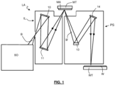
- Figure 1 shows a lithographic system comprising a radiation source SO and a lithographic apparatus LA.
- the radiation source SO is configured to generate an EUV radiation beam B and to supply the EUV radiation beam B to the lithographic apparatus LA.
- the lithographic apparatus LA comprises an illumination system IL, a support structure MT configured to support a patterning device MA (e.g., a mask), a projection system PS and a substrate table WT configured to support a substrate W.
- a patterning device MA e.g., a mask
- the illumination system IL is configured to condition the EUV radiation beam B before the EUV radiation beam B is incident upon the patterning device MA.
- the illumination system IL may include a facetted field mirror device 10 and a facetted pupil mirror device 11.
- the faceted field mirror device 10 and faceted pupil mirror device 11 together provide the EUV radiation beam B with a desired cross-sectional shape and a desired intensity distribution.
- the illumination system IL may include other mirrors or devices in addition to, or instead of, the faceted field mirror device 10 and faceted pupil mirror device 11.
- the EUV radiation beam B interacts with the patterning device MA. As a result of this interaction, a patterned EUV radiation beam B' is generated.
- the projection system PS is configured to project the patterned EUV radiation beam B' onto the substrate W.
- the projection system PS may comprise a plurality of mirrors 13,14 which are configured to project the patterned EUV radiation beam B' onto the substrate W held by the substrate table WT.
- the projection system PS may apply a reduction factor to the patterned EUV radiation beam B', thus forming an image with features that are smaller than corresponding features on the patterning device MA. For example, a reduction factor of 4 or 8 may be applied.
- the projection system PS is illustrated as having only two mirrors 13,14 in Figure 1 , the projection system PS may include a different number of mirrors (e.g. six or eight mirrors).
- the substrate W may include previously formed patterns. Where this is the case, the lithographic apparatus LA aligns the image, formed by the patterned EUV radiation beam B', with a pattern previously formed on the substrate W.
- a relative vacuum i.e. a small amount of gas (e.g. hydrogen) at a pressure well below atmospheric pressure, may be provided in the radiation source SO, in the illumination system IL, and/or in the projection system PS.
- gas e.g. hydrogen
- the radiation source SO may be a laser produced plasma (LPP) source, a discharge produced plasma (DPP) source, a free electron laser (FEL) or any other radiation source that is capable of generating EUV radiation.
- LPP laser produced plasma
- DPP discharge produced plasma
- FEL free electron laser
- Figure 2 depicts a control diagram of an optical system, such as a protection system of a lithographic apparatus.
- the projection system comprises N mirrors. N may be an integer > 1.
- Each mirror may comprise an actuator to control a mirror position of the mirror, the mirror position may be controlled by a respective feedback controller.
- a setpoint of the position of the mirror is provided by r 1 .
- Controller C 1 is comprised in a feedback control loop which controls a position of plant P 1 (the plant comprising the actuator which is configured to actuate the mirror, the mirror and a sensor which is configured to measure a position yi of the mirror.
- a sensor signal representative of the position of the mirror is compared to the position setpoint r 1 to generate an error signal e 1 which forms the input to the controller C 1 of the feedback loop.
- a position error in the present embodiment indicated as a line of sight error LoS 1 is determine by a multiplication of the error signal e 1 , which represents a difference between the mirror position setpoint and the measured mirror position, by the optical sensitivity S 1 of the first mirror S 1 .
- the optical sensitivity may be understood as a quotient of image position error over mirror position error.
- the image position error may be understood as a difference between the actual position of the image projected by the optical system and the desired position of the image projected by the optical system.
- the image position error may be understood as a difference between the position of the pattern on the substrate and the desired position of the pattern on the substrate.
- the optical system according to the present embodiment comprises n mirrors, whereby for each one of mirror 1 ...mirror m (m being n - 1), a respective position setpoint r, controller C, plant P, position y and error signal e is provided.
- the error signals e of the respective control loops are multiplied by the respective optical sensitivities to form respective line of sight errors.
- the line of sight errors of the mirrors 1 - m are summed to form a summed Line of Sight error LoS 1 ...m for mirrors 1 - m.
- the summed Line of Sight error of the mirrors 1 - m is fed through to a feedback control loop of mirror n, as follows:
- the summed Line of Sight error LoS 1 .. m is multiplied by an inverse of the optical sensitivity of mirror n S -1 n , and fed through to mirror n as follows:
- the summed Line of Sight error LoS 1 .. m multiplied by the inverse of the optical sensitivity of mirror n S -1 n is added to the setpoint r n of mirror n to form a reference for the nth mirror.
- the mirror n i.e. the nth mirror is provided with an additional setpoint to compensate for the line of sight error by the mirrors 1 ..
- the summed Line of Sight error LoS 1 .. m multiplied by an inverse of the optical sensitivity of mirror n S -1 n is filtered, such as using a low pass filter H lpm . Using the filter, a feed through of noise in the determined line of sight error of the mirrors 1 .. m, i.e. a feedthrough of such noise to mirror m, may be reduced.
- the summed Line of Sight error LoS 1 .. m multiplied by an inverse of the optical sensitivity of mirror n S -1 n is provided as a feedforward signal to the plant n.
- the summed Line of Sight error LoS 1 .. m multiplied by an inverse of the optical sensitivity of mirror n S -1 n after having been filtered by the filter H lpm is twice time differentiated and multiplied by a mass m n of the mirror n to generate a feedforward signal which is added to the output signal of the controller C n of mirror n.
- a line of sight error of the mirror n may be determined from the error signal e n of mirror n, or from the position y n and the combined reference inputs r n and feedthrough signal. Said signals may be multiplied by the optical sensitivity S n of mirror n.
- the line of sight error of mirror n aims to at least partly compensate the summed line of sight errors by mirrors 1 .. m.
- the line of image positioning error of optical component n aims to at least partly compensate the summed image positioning errors by optical components 1 .. m.
- Figure 3 depicts the same controllers of mirrors 1 .. n and further depicts a substrate table control system that controls a position of the substrate table.
- the optical image as projected by the mirror 1 .. n is projected onto a substrate W, the substrate W being held by substrate table W t .
- the substrate table is positioned by a respective actuator, which is controlled by a respective feedback controller.
- a setpoint of the position of the substrate table is provided by r ws .
- Controller C ws is comprised in a feedback control loop which controls a position of plant P ws (the plant comprising the actuator which is configured to actuate the substrate table, the substrate table and a sensor which is configured to measure a position y ws of the substrate table.
- a sensor signal representative of the position of the substrate table is compared to the position setpoint r ws to generate an error signal e ws which forms the input to the controller C ws of the feedback loop.
- a substrate table position error in the present embodiment indicated as the substrate table position error v ws is determined by a multiplication of the error signal e 1 , which represents a difference between the substrate table position setpoint and the measured substrate table position, by the optical sensitivity S ws of the substrate table Ws.
- the "LoS" signals may represent an impact of the mirror and stage positions on substrate level, not an impact of the position errors.
- the summation of reference x sensitivity of the optical components should result in a value of zero to arrive at a net zero Line of Sight error.
- the summation of error x sensitivity should likewise result in a value of zero to obtain a net zero Line of Sight error.
- the addition of the substrate table position v ws multiplied by the respective sensitivity and the mirror n position v n multiplied by the respective sensitivity to the position errors of the mirrors 1 .. m multiplied by the respective sensitivities may provide a summed line of sight error LoS 1 .. ws of the mirrors 1 .. n and the substrate table.
- the inventors have sought to further reduce an image positioning error. Thereto, the inventors have sought to further expand the above described feeding through to include the substrate table. More specifically, the inventors have sought to combine the feed through of mirrors 1 .. m to mirror n, with the substrate table, thus to at least partly compensate an image positioning error by the mirrors 1 .. n by the substrate table.
- the inventors have first attempted to feed through the summed line of sight error of mirrors 1 .. n to the substrate table WT. This approach however appeared to be incorrect. As may readily be understood, in case the compensation by mirror n would fully compensate the summed line of sight error from mirrors 1.. m, then the resulting line of sight error, or generally speaking the resulting image position error, would be zero. However, in line with the above described first attempt, the servo errors of the mirrors 1 ..m would also be sent to the substrate table, thereby attempting to compensate what has already been compensated before. Accordingly, the solution to include the substrate table did not provide to be as straightforward as initially devised.
- the inventors have devised a means to compensate by a third optical component, a remaining image positioning error when using a first optical component and a second optical component, whereby an image positioning error of the first optical component is fed through to the second optical component to at least partly compensate by the second optical component the image positioning error by the first optical component.
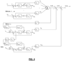
- Figure 4 depicts a further embodiment of an optical system, whereby instead of feeding through the line of sight error of all mirrors 1 .. n to the substrate table, only the line of sight error of mirror n is fed through to the substrate table.
- the image positioning error of the first component and the image positioning error of the second component instead of feeding through the image positioning error of the first component and the image positioning error of the second component to the third component, only the image positioning error of the second component is fed through to the third component.
- Figure 4 depicts the control of the mirrors 1 .. m and mirror n as described above with reference to Figures 2 and 3 . Furthermore, the line of sight error of the mirror n is fed through to the substrate table . In general terms, the image positioning error of the second component is fed through to the third component.
- the error signal e n in the feedback control loop of mirror n is multiplied by an optical sensitivity of the mirror n and multiplied by an inverse optical sensitivity S -1 ws of the substrate table, the resulting signal being fed through to the substrate table.
- a filter is applied for reduction of noise effects, such as in the present example the low pass filter H lpws .
- the filtered signal is fed through to the substrate table, namely by addition to the setpoint r ws of the substrate table.
- the Line of Sight error LoS n multiplied by an inverse of the optical sensitivity of the substrate table S -1 ws is provided as a feedforward signal to the substrate table plant P ws .
- the Line of Sight error LoS nm multiplied by an inverse of the optical sensitivity of the substrate table S -1 ws after having been filtered by the filter H lpm is twice time-differentiated and multiplied by a mass m ws of the substrate table to generate a feedforward signal which is added to the output signal of the controller C ws of the substrate table.
- the multiplications by the optical sensitivity respectively the inverse optical sensitivity may enable to take account of differences in optical sensitivity of the first second and third components.
- the filter H lpws may promote a suppression of noise and/or other undesired effects, it also appears to affect the compensation in that, for example in the case of a low pass filter, a high frequency content in the error may be suppressed.
- dynamic performance may be affected by a delay associated with the filter.
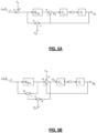
- Figures 5 A and 5B depict partial control diagrams illustrating a generation of the feedthrough signal from mirror n to the substrate table, in other words the generation of the feedthrough signal from the second component to the third component.
- the feed through signal r ft is determined from the line of sight error of the mirrors 1 - m, plus the setpoint of mirror n, minus the output of the mirror n (i.e. the actual position of mirror n).
- the image positioning error of the second component is determined from the image positioning error of the first component plus the setpoint of the second component minus the output of the second component.
- the feed through signal r ft is determined from the line of sight error of the mirrors 1 - m, minus the filtered line of sight error of the mirrors 1 - m, plus the servo error of the mirror n.
- the image positioning error of the second component is determined from the image positioning error of the first component minus a filtered image positioning error of the first component plus the servo error of the second component.
- the feed through signal may be determined taking account of the filter, thereby enabling the filter to suppress undesired effects such as noise, however at least partly avoiding a deterioration by the filter on the feedthrough signal.
- Figures 2 - 5B generally refer to an optical system comprising a first component comprising mirrors 1 .. n, a second component comprising mirror n and a third component comprising a substrate table
- the present development may be applied to any suitable combination of optical components.
- one or more of the components may comprise a mirror or a set of mirrors.
- One of the components may comprise a substrate table.
- One of the components may comprise a patterning device that imparts the projection optical beam with a pattern to be projected onto the substrate.
- the optical system according to the present development may be comprised in a lithographic apparatus.
- the first component may comprise mirrors 1 - m (m being n-1)
- the second component may comprise mirror n
- the third component may comprise the substrate table or the support of the patterning device.
- the image positioning error in the first component in this example mirror 1 - m
- the second component in this example mirror m
- the image positioning error of the second component may be fed through to the third component (in this example the support of the patterning device or the substrate table).
- a remaining image positioning error in the first component is at least partly corrected by the second component
- a remaining image positioning error in the second component is at least partly corrected by the third component.
- An overall image positioning error may be reduced, as the feed through of the image positioning error in the second component to the third component at least compensates the image positioning error in the second component, which may comprise an at least partial compensation of a remainder of the image positioning error in the first component which is not yet compensated by the second component.
- lithographic apparatus in the manufacture of ICs, it should be understood that the lithographic apparatus described herein may have other applications. Possible other applications include the manufacture of integrated optical systems, guidance and detection patterns for magnetic domain memories, flat-panel displays, liquid-crystal displays (LCDs), thin-film magnetic heads, etc.
- Embodiments of the invention may form part of a mask inspection apparatus, a metrology apparatus, or any apparatus that measures or processes an object such as a wafer (or other substrate) or mask (or other patterning device). These apparatus may be generally referred to as lithographic tools. Such a lithographic tool may use vacuum conditions or ambient (non-vacuum) conditions.
- embodiments of the invention may be implemented in hardware, firmware, software, or any combination thereof. Embodiments of the invention may also be implemented as instructions stored on a machine-readable medium, which may be read and executed by one or more processors.
- a machine-readable medium may include any mechanism for storing or transmitting information in a form readable by a machine (e.g., a computing device).
- a machine-readable medium may include read only memory (ROM); random access memory (RAM); magnetic storage media; optical storage media; flash memory devices; electrical, optical, acoustical or other forms of propagated signals (e.g. carrier waves, infrared signals, digital signals, etc.), and others.
- firmware, software, routines, instructions may be described herein as performing certain actions.
Landscapes
- Physics & Mathematics (AREA)
- General Physics & Mathematics (AREA)
- Exposure And Positioning Against Photoresist Photosensitive Materials (AREA)
Priority Applications (5)
| Application Number | Priority Date | Filing Date | Title |
|---|---|---|---|
| EP23169554.5A EP4455784A1 (de) | 2023-04-24 | 2023-04-24 | Verfahren und system zur bildpositionierungssteuerung |
| PCT/EP2024/056751 WO2024223142A1 (en) | 2023-04-24 | 2024-03-14 | Image positioning control method and system |
| KR1020257035502A KR20260002764A (ko) | 2023-04-24 | 2024-03-14 | 이미지 위치설정 제어 방법 및 시스템 |
| CN202480027529.4A CN121038923A (zh) | 2023-04-24 | 2024-03-14 | 图像定位控制方法和系统 |
| TW113112480A TW202509673A (zh) | 2023-04-24 | 2024-04-02 | 影像定位控制方法及系統 |
Applications Claiming Priority (1)
| Application Number | Priority Date | Filing Date | Title |
|---|---|---|---|
| EP23169554.5A EP4455784A1 (de) | 2023-04-24 | 2023-04-24 | Verfahren und system zur bildpositionierungssteuerung |
Publications (1)
| Publication Number | Publication Date |
|---|---|
| EP4455784A1 true EP4455784A1 (de) | 2024-10-30 |
Family
ID=86185262
Family Applications (1)
| Application Number | Title | Priority Date | Filing Date |
|---|---|---|---|
| EP23169554.5A Withdrawn EP4455784A1 (de) | 2023-04-24 | 2023-04-24 | Verfahren und system zur bildpositionierungssteuerung |
Country Status (5)
| Country | Link |
|---|---|
| EP (1) | EP4455784A1 (de) |
| KR (1) | KR20260002764A (de) |
| CN (1) | CN121038923A (de) |
| TW (1) | TW202509673A (de) |
| WO (1) | WO2024223142A1 (de) |
Cited By (1)
| Publication number | Priority date | Publication date | Assignee | Title |
|---|---|---|---|---|
| EP4567514A2 (de) | 2025-03-27 | 2025-06-11 | ASML Netherlands B.V. | Belichtungsapparatpositionssteuerung |
Citations (3)
| Publication number | Priority date | Publication date | Assignee | Title |
|---|---|---|---|---|
| US20170363965A1 (en) * | 2014-12-01 | 2017-12-21 | Asml Netherlands B.V. | Projection system |
| US20190310557A1 (en) * | 2016-12-21 | 2019-10-10 | Carl Zeiss Smt Gmbh | Lithography system and method |
| US20220132038A1 (en) * | 2019-07-15 | 2022-04-28 | Huawei Technologies Co., Ltd. | Photographic apparatus and method of operating a photographic apparatus for jitter reduction |
-
2023
- 2023-04-24 EP EP23169554.5A patent/EP4455784A1/de not_active Withdrawn
-
2024
- 2024-03-14 WO PCT/EP2024/056751 patent/WO2024223142A1/en not_active Ceased
- 2024-03-14 KR KR1020257035502A patent/KR20260002764A/ko active Pending
- 2024-03-14 CN CN202480027529.4A patent/CN121038923A/zh active Pending
- 2024-04-02 TW TW113112480A patent/TW202509673A/zh unknown
Patent Citations (3)
| Publication number | Priority date | Publication date | Assignee | Title |
|---|---|---|---|---|
| US20170363965A1 (en) * | 2014-12-01 | 2017-12-21 | Asml Netherlands B.V. | Projection system |
| US20190310557A1 (en) * | 2016-12-21 | 2019-10-10 | Carl Zeiss Smt Gmbh | Lithography system and method |
| US20220132038A1 (en) * | 2019-07-15 | 2022-04-28 | Huawei Technologies Co., Ltd. | Photographic apparatus and method of operating a photographic apparatus for jitter reduction |
Cited By (1)
| Publication number | Priority date | Publication date | Assignee | Title |
|---|---|---|---|---|
| EP4567514A2 (de) | 2025-03-27 | 2025-06-11 | ASML Netherlands B.V. | Belichtungsapparatpositionssteuerung |
Also Published As
| Publication number | Publication date |
|---|---|
| WO2024223142A1 (en) | 2024-10-31 |
| CN121038923A (zh) | 2025-11-28 |
| KR20260002764A (ko) | 2026-01-06 |
| TW202509673A (zh) | 2025-03-01 |
Similar Documents
| Publication | Publication Date | Title |
|---|---|---|
| CN101320223B (zh) | 光刻设备、控制方法以及标定方法 | |
| US7576832B2 (en) | Lithographic apparatus and device manufacturing method | |
| KR100869308B1 (ko) | 리소그래피 장치 및 디바이스 제조 방법 | |
| US8279401B2 (en) | Position control system, a lithographic apparatus and a method for controlling a position of a movable object | |
| EP4455784A1 (de) | Verfahren und system zur bildpositionierungssteuerung | |
| US20250053102A1 (en) | Method of reducing cyclic error effects in a lithographic process, projection system and lithographic apparatus comprising a projection system | |
| US7084958B2 (en) | Lithographic apparatus, control system and device manufacturing method | |
| JP6679722B2 (ja) | リソグラフィ装置および方法 | |
| NL2020474A (en) | Lithographic system, euv radiation source, lithographic scanning apparatus and control system | |
| JP2008047897A (ja) | リソグラフィ装置、放射源、放射源コントローラおよび制御方法 | |
| US20260016757A1 (en) | Control method and control system for controlling a position of an object with an electromagnetic actuator | |
| US7847919B2 (en) | Lithographic apparatus having feedthrough control system | |
| EP4722807A1 (de) | Lithographisches projektionsverfahren und lithographische vorrichtung | |
| EP4455785A1 (de) | Verfahren und system zur steuerung der position eines optischen elements | |
| US11454938B2 (en) | Control system, method to increase a bandwidth of a control system, and lithographic apparatus | |
| US20250291260A1 (en) | Method of determining a parasitic force of an actuator of an optical component, control method for an actuator, optical system, projection system and lithographic apparatus. | |
| US11550227B2 (en) | Projection system and lithographic apparatus comprising said projection system | |
| EP4567514A2 (de) | Belichtungsapparatpositionssteuerung |
Legal Events
| Date | Code | Title | Description |
|---|---|---|---|
| PUAI | Public reference made under article 153(3) epc to a published international application that has entered the european phase |
Free format text: ORIGINAL CODE: 0009012 |
|
| STAA | Information on the status of an ep patent application or granted ep patent |
Free format text: STATUS: THE APPLICATION HAS BEEN PUBLISHED |
|
| AK | Designated contracting states |
Kind code of ref document: A1 Designated state(s): AL AT BE BG CH CY CZ DE DK EE ES FI FR GB GR HR HU IE IS IT LI LT LU LV MC ME MK MT NL NO PL PT RO RS SE SI SK SM TR |
|
| STAA | Information on the status of an ep patent application or granted ep patent |
Free format text: STATUS: THE APPLICATION IS DEEMED TO BE WITHDRAWN |
|
| 18D | Application deemed to be withdrawn |
Effective date: 20250501 |