EP4455616A1 - Resolver quadrant detection - Google Patents
Resolver quadrant detection Download PDFInfo
- Publication number
- EP4455616A1 EP4455616A1 EP24173157.9A EP24173157A EP4455616A1 EP 4455616 A1 EP4455616 A1 EP 4455616A1 EP 24173157 A EP24173157 A EP 24173157A EP 4455616 A1 EP4455616 A1 EP 4455616A1
- Authority
- EP
- European Patent Office
- Prior art keywords
- resolver
- output
- coil
- quadrant
- operatively connected
- Prior art date
- Legal status (The legal status is an assumption and is not a legal conclusion. Google has not performed a legal analysis and makes no representation as to the accuracy of the status listed.)
- Pending
Links
Images




Classifications
-
- G—PHYSICS
- G01—MEASURING; TESTING
- G01D—MEASURING NOT SPECIALLY ADAPTED FOR A SPECIFIC VARIABLE; ARRANGEMENTS FOR MEASURING TWO OR MORE VARIABLES NOT COVERED IN A SINGLE OTHER SUBCLASS; TARIFF METERING APPARATUS; MEASURING OR TESTING NOT OTHERWISE PROVIDED FOR
- G01D5/00—Mechanical means for transferring the output of a sensing member; Means for converting the output of a sensing member to another variable where the form or nature of the sensing member does not constrain the means for converting; Transducers not specially adapted for a specific variable
- G01D5/12—Mechanical means for transferring the output of a sensing member; Means for converting the output of a sensing member to another variable where the form or nature of the sensing member does not constrain the means for converting; Transducers not specially adapted for a specific variable using electric or magnetic means
- G01D5/14—Mechanical means for transferring the output of a sensing member; Means for converting the output of a sensing member to another variable where the form or nature of the sensing member does not constrain the means for converting; Transducers not specially adapted for a specific variable using electric or magnetic means influencing the magnitude of a current or voltage
- G01D5/20—Mechanical means for transferring the output of a sensing member; Means for converting the output of a sensing member to another variable where the form or nature of the sensing member does not constrain the means for converting; Transducers not specially adapted for a specific variable using electric or magnetic means influencing the magnitude of a current or voltage by varying inductance, e.g. by a movable armature
- G01D5/204—Mechanical means for transferring the output of a sensing member; Means for converting the output of a sensing member to another variable where the form or nature of the sensing member does not constrain the means for converting; Transducers not specially adapted for a specific variable using electric or magnetic means influencing the magnitude of a current or voltage by varying inductance, e.g. by a movable armature by influencing the mutual induction between two or more coils
- G01D5/2073—Mechanical means for transferring the output of a sensing member; Means for converting the output of a sensing member to another variable where the form or nature of the sensing member does not constrain the means for converting; Transducers not specially adapted for a specific variable using electric or magnetic means influencing the magnitude of a current or voltage by varying inductance, e.g. by a movable armature by influencing the mutual induction between two or more coils by movement of a single coil with respect to two or more coils
Definitions
- the present disclosure relates to resolvers for sensing angular position or speed, and more particularly to resolvers for detecting angular position and speed of motor shafts, actuators, servos, or the like.
- the resolver signals can be interfaced to an analog to digital converter (ADC) without rectification (full bipolar swing).
- ADC data is used by a processor, e.g. a field programmable gated array (FPGA), to calculate the resolver position and speed.
- FPGA field programmable gated array
- the resolver can be interfaced to a resolver-to-digital converter (RDC) chip.
- RDC resolver-to-digital converter
- the resolver angle computation requires the excitation, sine, and cosine signal amplitudes and their relative phases to determine the angle quadrant (among quadrants I to IV, e.g. where quadrant I is a position between 0-degrees and 90-degrees).
- the full bipolar signal swing is applied to the ADC, though only half of the signal swing is sufficient to determine the amplitude. So, effectively half of the ADC dynamic range is not used.
- the angle quadrant information would be lost. The same issues also translate to the RDC configuration above.
- a system includes first precision rectifier operatively connected to receive high and low signals of a sine coil of a resolver and to output a first signaled condition.
- a second precision rectifier is operatively connected to receive high and low signals of a cosine coil of the resolver and to output a second signaled condition.
- a quadrant detection circuit operatively connected to receive high and low signals of the exciter coil of the resolver, wherein the quadrant detection circuit is operatively connected to receive high and low signals from the sine coil and from the cosine coil, and to output a signal indicative of quadrant position of the resolver.
- the resolver can include the sine coil, the cosine coil, and the exciter coil, wherein the exciter coil is configured to rotate relative to the sine coil and cosine coil which are stationary relative to one another.
- a resolver exciter can be operatively connected to excite the exciter coil, and to provide the high and low signals of the exciter coil to the quadrant detection circuit.
- a processing device can be operatively connected to control the exciter.
- An analog to digital converter (ADC) component can be operatively connected to receive the first signaled condition, the second signaled condition, and the signal indicative of quadrant position of the resolver, and to output a digital signal.
- the ADC component can include one ADC with three input channels, one input channel for each of the first signaled condition, the second signaled condition, and the signal indicative of quadrant position of the resolver.
- the ADC component can include: a first ADC operatively connected to receive the first signaled condition and to output a first digital signal for determining quadrant position of the resolver to the processing device; a second ADC operatively connected to receive the second signaled condition and to output a second digital signal for determining quadrant position of the resolver to the processing device; and a third ADC operatively connected to receive the signal indicative of quadrant position of the resolver and to output a digital signal for determining quadrant position of the resolver to the processing device.
- a first filter can be configured to receive the high and low signals of a sine coil of the resolver and to output respective filtered high and low sine coil signals.
- a second filter can be configured to receive the high and low signals of the cosine coil of the resolver and to output respective filtered high and low cosine coil signals.
- a multi-channel analog multiplexer can be operatively connected to receive filtered output from the first and second filters, to receive the signal indicative of quadrant position of the resolver from the quadrant detection circuit, and to output one or more multiplexed signals.
- a differential to single ended converter can be operatively connected to receive the one or more multiplexed signals and to output a single analog signal.
- a precision rectifier can be operatively connected to receive the single analog signal and to output a rectified single signal.
- An analog to digital converter (ADC) can be operatively connected to receive the rectified single signal and to output a digital signal indicative of resolver position to the processing device.
- the quadrant detection circuit can include logic configured to output a signal indicative of resolver position in a first quadrant upon receiving high input of the sine coil, high input of the cosine coil, and high input of the exciter coil.
- the logic can be configured to output a signal indicative of resolver position in a second quadrant upon receiving high input of the sine coil, low input of the cosine coil, and high input of the exciter coil.
- the logic can be configured to output a signal indicative of resolver position in a third quadrant upon receiving low input of the sine coil, low input of the cosine coil, and high input of the exciter coil.
- the logic can be configured to output a signal indicative of resolver position in a fourth quadrant upon receiving low input of the sine coil, high input of the cosine coil, and high input of the exciter coil.
- the quadrant detection circuit can include a first zero crossing detector for the high and low signals of the exciter coil configured to output a high or low output for the exciter coil.
- a second zero crossing detector for the high and low signals of the sine coil can be configured to output a high or low output for the sine coil.
- a third zero crossing detector for the high and low signals of the cosine coil can be configured to output a high or low signal for the cosine coil.
- the logic can be configured to determine quadrant position of the resolver based on output from the first, second, and third zero crossing detectors.
- the logic can include PWM generator configured to output a PWM signal with a respective predetermined duty cycle representative of each of the respective four quadrants of the quadrant position of the resolver.
- the processing device can be configured to interpret a digital representation of the PWM signal into a quadrant position of the resolver, and to provide output indicative of angular speed and/or position of the resolver.
- TABLE 1 is a truth table for determining quadrant position of the resolver based on inputs from the sine and cosine coils.
- FIG. 1 a partial view of an embodiment of a system in accordance with the disclosure is shown in Fig. 1 and is designated generally by reference character 100.
- Other embodiments of systems in accordance with the disclosure, or aspects thereof, are provided in Figs. 2-5 and TABLE 1, as will be described.
- the systems and methods described herein can be used to determine in which quadrant a resolver is positioned for angular position and angular speed measurements.
- This disclosure describes a method by which a resolver can be interfaced using a unipolar signal swing in a precision rectifier based data acquisition system.
- SNR signal to noise ratio
- ADC analog to digital converter
- Four quadrants can be represented in a single signal, e.g., if the signal is pulse width modulated (PWM).
- PWM pulse width modulated
- a quadrant detection circuit which accepts excitation, sine, and cosine, can generate a PWM output based on the phase difference of the signals, which output can be used to represent the resolver quadrant.
- the system 100 includes a resolver 102.
- the resolver 102 includes the sine coil 104, the cosine coil, 106 and the exciter coil 108.
- the exciter coil 108 is configured to rotate, as indicated by the double-headed, curved arrow in Fig. 1 , relative to the sine coil 104 and cosine coil 106, which are stationary relative to one another.
- the resolver 102 can be a rotary transformer type as depicted in Fig. 1 , or a variable reluctance type with no rotor winding, without departing from the scope of this invention as defined by the claims.
- a resolver exciter 110 is operatively connected to excite the exciter coil 108, and to provide the high and low signals of the exciter coil 108 to the quadrant detection circuit 112, shown in Figs. 2-5 .
- a processing device 114 such as a processor, field programmable gate array (FPGA), or the like, is operatively connected to control the exciter 110.
- a sensor signal processing block 116 is connected between the coils 104, 106, 108 and the processing device 114, as described below with respect to Figs. 2-4 .
- a first precision rectifier 118 is operatively connected to receive high and low signals of the sine coil of a resolver and to output a signaled condition 120 indicative of precision rectified output of the input signal to the first precision rectifier 118.
- a second precision rectifier 122 is operatively connected to receive high and low signals of the cosine coil 106 of the resolver 102 of Fig. 1 , and to output a signaled condition 124 indicative of precision rectified output of the input signal received by the second precision rectifier 122.
- the quadrant detection circuit 112 is operatively connected to receive high and low signals of the exciter coil 108, as well as the high and low signals of the sine and cosine coils 104, 106.
- the quadrant detection circuit 112 is configured to output a pulse width modulated (PWM) signal 126 indicative of quadrant position of the resolver 102 of Fig. 1 .
- PWM pulse width modulated
- an analog to digital converter (ADC) component 128 is operatively connected to receive the signaled conditions 120, 124 indicative of relative phase of the sine and cosine coils 104, 106, and the signal 126 indicative of quadrant position, and to output a digital signal 130 to the processing device 114 indicative of resolver position, including quadrant data.
- the Processor/FPGA communicates ADC configuration data and also typically the clock signal which synchronizes the data transfer over the, e.g. serial peripheral interface (SPI), bus.
- the ADC component 128 in Fig. 2 includes one ADC with three input channels, one input channel for each of the signaled conditions 120, 124, and one channel for the signal 126 indicative of quadrant position of the resolver.
- the ADC component in Fig. 3 includes three separate one channel ADCs 128a, 128b, 128c.
- the first ADC 128a is operatively connected to receive the signaled condition 120 and to output a first digital signal to the processing device 114.
- the second ADC 128b is operatively connected to receive the signaled condition 124 and to output a second digital signal to the processing device 114.
- the third ADC 128c is operatively connected to receive the signal 126 indicative of quadrant position of the resolver and to output a third digital signal for determining quadrant position of the resolver to the processing device 114.
- the signal 126 can also be used for timer input to the processing device as indicated by the arrow with the broken lines.
- the PWM duty cycle can be measured by the timer block and using the measurement from CH-2 and CH-3 the position and speed can be calculated (note that CH-1, Ch-2, and CH-3 are shown in Fig. 2 , and in Fig. 3 these are ADC-1, ADC-2, and ADC-3, respectively). If is desired to measure only the speed, then speed can be easily found out by connecting signal 126 to the timer.
- a filter 132 is configured to receive the high and low signals of the sine coil 104 and to output respective filtered high and low sine coil signals to multi-channel analog multiplexor 134.
- a filter 136 is configured to receive the high and low signals of the cosine coil 106 and to output respective filtered high and low cosine coil signals to the multi-channel analog multiplexor 134.
- the multi-channel analog multiplexer is operatively connected to receive the filtered output from the filters 132, 136, to receive the signal 126 indicative of quadrant position from the quadrant detection circuit 112, and potentially any suitable number of other inputs 138 (e.g.
- OUT_A and OUT_B carry the selected differential signal out of all the signals at the input of the analog multiplexer 134.
- the signal is selected by the FPGA/ Processor 114 by switching the multiplexer channel (those control signals from the FPG/Processor 114 to the multiplexor 134 are not shown in Fig. 4 ).
- the FPGA/ Processor 114 typically does a round robin selection of the multiplexer inputs, starting from the first input channel and then sequencing through the rest so that each analog input can be sequentially digitized by the ADC 128.
- a differential to single ended converter 140 is operatively connected to receive OUT_A and OUT_B and to output a single ended analog signal 142.
- a precision rectifier 144 is operatively connected to receive the single ended analog signal 142 and to output a rectified single signal 146.
- An ADC 128 is operatively connected to receive the rectified single signal 146 and to output a digital signal 130 indicative of resolver position, including quadrant location, to the processing device 114.
- the quadrant detection circuit 112 includes a first zero crossing detector 148 for the high and low signals of the exciter coil 108 configured to output a logic level high or logic level low output for the exciter coil 108 to the logic 150.
- a second zero crossing detector 152 for the high and low signals of the sine coil is configured to output a logic level high or logic level low output for the sine coil 104 to the logic 150.
- a third zero crossing detector 154 for the logic level high and logic level low signals of the cosine coil 106 is configured to output a high or low signal for the cosine coil 106 to the logic.
- the logic 150 of the quadrant detection circuit 112 is configured to determine quadrant position of the resolver 102 (labeled in Fig.
- the logic 150 includes PWM generator 156 configured to output a PWM signal 126 with a respective predetermined duty cycle, e.g. the percentages listed in the fourth column of TABLE 1, representative of each of the respective four quadrants of the quadrant position of the resolver 102 labeled in Fig. 1 .
- the processing device 114 (labeled in Figs. 1-4 ) is configured to interpret a digital representation of the PWM signal 126 into a quadrant position of the resolver 102 (labeled in Fig. 1 ), and to provide output 158 (labeled in Fig. 1 ), e.g. for use as feedback in a control circuit or the like, indicative of angular speed and/or position of the resolver 102 (labeled in Fig. 1 ).
- logic 150 is configured to output a signal 126 indicative of resolver position in a first quadrant, e.g. between 0-degrees to 90-degrees, upon receiving high input of zero crossing detector 152 of the sine coil (hereafter abbreviated to high input of the sine coil, and low input of the zero crossing detector 152 is hereafter abbreviated to low input of the sine coil), high input of zero crossing detector 154 of the cosine coil (hereafter abbreviated to high input of the cosine coil, and low input of the zero crossing detector 154 is hereafter abbreviated to low input of the cosine coil), and high input of the zero crossing detector 148 of the exciter coil (hereafter high input of the exciter coil, and low input of the zero crossing detector 148 is hereafter referred to as low input of the exciter coil), as indicated in the first row of TABLE 1.
- the logic 150 is configured to output a signal 126 indicative of resolver position in a second quadrant, e.g. between 90-degrees to 180-degrees, upon receiving high input zero of the sine coil, low input of the cosine coil, and high input of the exciter coil, as indicated in the second row of TABLE 1.
- the logic 150 is configured to output a signal 126 indicative of resolver position in a third quadrant, e.g. between 180-degrees to 270-degrees, upon receiving low input of the sine coil, low input of the cosine coil, and high input of the exciter coil, as indicated in the third row of TABLE 1.
- the logic 150 is configured to output a signal 126 indicative of resolver position in a fourth quadrant, e.g.
- the logic 150 can include any suitable type of logic such as analog circuit components, digital circuit components, digital processing devices with machine readable instructions, or the like, configured to perform the functions described herein.
- This disclosure describes a method by which the resolver can be interfaced using a unipolar signal swing in a precision rectifier based data acquisition system.
- SNR Signal to Noise ratio
- Effective bit resolution can be derived by use of the full ADC dynamic range.
- Quadrant detection output alone can also be used for speed and direction measurement in applications where position measurement is not required.
Landscapes
- Physics & Mathematics (AREA)
- General Physics & Mathematics (AREA)
- Transmission And Conversion Of Sensor Element Output (AREA)
Abstract
Description
- The present disclosure relates to resolvers for sensing angular position or speed, and more particularly to resolvers for detecting angular position and speed of motor shafts, actuators, servos, or the like.
- Resolvers are traditionally interfaced in the following ways. First, the resolver signals can be interfaced to an analog to digital converter (ADC) without rectification (full bipolar swing). ADC data is used by a processor, e.g. a field programmable gated array (FPGA), to calculate the resolver position and speed. Second, the resolver can be interfaced to a resolver-to-digital converter (RDC) chip. The chip provides resolver position and speed.
- In the ADC configuration above, the resolver angle computation requires the excitation, sine, and cosine signal amplitudes and their relative phases to determine the angle quadrant (among quadrants I to IV, e.g. where quadrant I is a position between 0-degrees and 90-degrees). The full bipolar signal swing is applied to the ADC, though only half of the signal swing is sufficient to determine the amplitude. So, effectively half of the ADC dynamic range is not used. To utilize the full ADC dynamic range, if the signals are precision rectified and a unipolar signal swing is directly used then the angle quadrant information would be lost. The same issues also translate to the RDC configuration above.
- The conventional techniques have been considered satisfactory for their intended purpose. However, there is an ever present need for improved systems and methods for quadrant detection in resolvers. This disclosure provides a solution for this need.
- A system includes first precision rectifier operatively connected to receive high and low signals of a sine coil of a resolver and to output a first signaled condition. A second precision rectifier is operatively connected to receive high and low signals of a cosine coil of the resolver and to output a second signaled condition. A quadrant detection circuit operatively connected to receive high and low signals of the exciter coil of the resolver, wherein the quadrant detection circuit is operatively connected to receive high and low signals from the sine coil and from the cosine coil, and to output a signal indicative of quadrant position of the resolver.
- The resolver can include the sine coil, the cosine coil, and the exciter coil, wherein the exciter coil is configured to rotate relative to the sine coil and cosine coil which are stationary relative to one another. A resolver exciter can be operatively connected to excite the exciter coil, and to provide the high and low signals of the exciter coil to the quadrant detection circuit. A processing device can be operatively connected to control the exciter.
- An analog to digital converter (ADC) component can be operatively connected to receive the first signaled condition, the second signaled condition, and the signal indicative of quadrant position of the resolver, and to output a digital signal. The ADC component can include one ADC with three input channels, one input channel for each of the first signaled condition, the second signaled condition, and the signal indicative of quadrant position of the resolver. The ADC component can include: a first ADC operatively connected to receive the first signaled condition and to output a first digital signal for determining quadrant position of the resolver to the processing device; a second ADC operatively connected to receive the second signaled condition and to output a second digital signal for determining quadrant position of the resolver to the processing device; and a third ADC operatively connected to receive the signal indicative of quadrant position of the resolver and to output a digital signal for determining quadrant position of the resolver to the processing device.
- A first filter can be configured to receive the high and low signals of a sine coil of the resolver and to output respective filtered high and low sine coil signals. A second filter can be configured to receive the high and low signals of the cosine coil of the resolver and to output respective filtered high and low cosine coil signals. A multi-channel analog multiplexer can be operatively connected to receive filtered output from the first and second filters, to receive the signal indicative of quadrant position of the resolver from the quadrant detection circuit, and to output one or more multiplexed signals. A differential to single ended converter can be operatively connected to receive the one or more multiplexed signals and to output a single analog signal. A precision rectifier can be operatively connected to receive the single analog signal and to output a rectified single signal. An analog to digital converter (ADC) can be operatively connected to receive the rectified single signal and to output a digital signal indicative of resolver position to the processing device.
- The quadrant detection circuit can include logic configured to output a signal indicative of resolver position in a first quadrant upon receiving high input of the sine coil, high input of the cosine coil, and high input of the exciter coil. The logic can be configured to output a signal indicative of resolver position in a second quadrant upon receiving high input of the sine coil, low input of the cosine coil, and high input of the exciter coil. The logic can be configured to output a signal indicative of resolver position in a third quadrant upon receiving low input of the sine coil, low input of the cosine coil, and high input of the exciter coil. The logic can be configured to output a signal indicative of resolver position in a fourth quadrant upon receiving low input of the sine coil, high input of the cosine coil, and high input of the exciter coil.
- The quadrant detection circuit can include a first zero crossing detector for the high and low signals of the exciter coil configured to output a high or low output for the exciter coil. A second zero crossing detector for the high and low signals of the sine coil can be configured to output a high or low output for the sine coil. A third zero crossing detector for the high and low signals of the cosine coil can be configured to output a high or low signal for the cosine coil. The logic can be configured to determine quadrant position of the resolver based on output from the first, second, and third zero crossing detectors. The logic can include PWM generator configured to output a PWM signal with a respective predetermined duty cycle representative of each of the respective four quadrants of the quadrant position of the resolver. The processing device can be configured to interpret a digital representation of the PWM signal into a quadrant position of the resolver, and to provide output indicative of angular speed and/or position of the resolver.
- These and other features of the systems and methods of the subject disclosure will become more readily apparent to those skilled in the art from the following detailed description of the preferred embodiments taken in conjunction with the drawings.
- So that those skilled in the art to which the subject disclosure appertains will readily understand how to make and use the devices and methods of the subject disclosure without undue experimentation, preferred embodiments thereof will be described in detail herein below with reference to certain figures, wherein:
-
Fig. 1 is a schematic view of an embodiment of a system constructed in accordance with the present disclosure, showing the resolver and sensor signal processing block; -
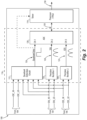
Fig. 2 is a schematic view of a portion of the system ofFig. 1 , showing an embodiment of the sensor signal processing block with one analog to digital converter (ADC) with three input channels; -
Fig. 3 is a schematic view of a portion of the system ofFig. 1 , showing an embodiment of the sensor signal processing block with three separate ADC's, each with a single input channel; -
Fig. 4 is a schematic view of a portion of the system ofFig. 1 , showing an embodiment of the sensor signal processing block with a multi-channel analog multiplexer; and -
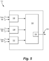
Fig. 5 is a schematic view of the quadrant detection circuit ofFigs. 2-4 . - TABLE 1 is a truth table for determining quadrant position of the resolver based on inputs from the sine and cosine coils.
- Reference will now be made to the drawings wherein like reference numerals identify similar structural features or aspects of the subject disclosure. For purposes of explanation and illustration, and not limitation, a partial view of an embodiment of a system in accordance with the disclosure is shown in
Fig. 1 and is designated generally byreference character 100. Other embodiments of systems in accordance with the disclosure, or aspects thereof, are provided inFigs. 2-5 and TABLE 1, as will be described. The systems and methods described herein can be used to determine in which quadrant a resolver is positioned for angular position and angular speed measurements. - This disclosure describes a method by which a resolver can be interfaced using a unipolar signal swing in a precision rectifier based data acquisition system. Thereby the benefit of improved signal to noise ratio (SNR) and effective bit resolution can be derived by use of the full analog to digital converter (ADC) dynamic range. Four quadrants can be represented in a single signal, e.g., if the signal is pulse width modulated (PWM). A quadrant detection circuit, which accepts excitation, sine, and cosine, can generate a PWM output based on the phase difference of the signals, which output can be used to represent the resolver quadrant.
- The
system 100 includes aresolver 102. Theresolver 102 includes thesine coil 104, the cosine coil, 106 and theexciter coil 108. Theexciter coil 108 is configured to rotate, as indicated by the double-headed, curved arrow inFig. 1 , relative to thesine coil 104 andcosine coil 106, which are stationary relative to one another. Those skilled in the art will readily appreciate that theresolver 102 can be a rotary transformer type as depicted inFig. 1 , or a variable reluctance type with no rotor winding, without departing from the scope of this invention as defined by the claims. Aresolver exciter 110 is operatively connected to excite theexciter coil 108, and to provide the high and low signals of theexciter coil 108 to thequadrant detection circuit 112, shown inFigs. 2-5 . Aprocessing device 114, such as a processor, field programmable gate array (FPGA), or the like, is operatively connected to control theexciter 110. A sensorsignal processing block 116 is connected between thecoils processing device 114, as described below with respect toFigs. 2-4 . - Referring now to
Fig. 2 , afirst precision rectifier 118 is operatively connected to receive high and low signals of the sine coil of a resolver and to output a signaledcondition 120 indicative of precision rectified output of the input signal to thefirst precision rectifier 118. Asecond precision rectifier 122 is operatively connected to receive high and low signals of thecosine coil 106 of theresolver 102 ofFig. 1 , and to output a signaledcondition 124 indicative of precision rectified output of the input signal received by thesecond precision rectifier 122. Thequadrant detection circuit 112 is operatively connected to receive high and low signals of theexciter coil 108, as well as the high and low signals of the sine andcosine coils quadrant detection circuit 112 is configured to output a pulse width modulated (PWM) signal 126 indicative of quadrant position of theresolver 102 ofFig. 1 . - With continued reference to
Fig. 2 , an analog to digital converter (ADC)component 128 is operatively connected to receive the signaledconditions cosine coils signal 126 indicative of quadrant position, and to output adigital signal 130 to theprocessing device 114 indicative of resolver position, including quadrant data. The Processor/FPGA communicates ADC configuration data and also typically the clock signal which synchronizes the data transfer over the, e.g. serial peripheral interface (SPI), bus. TheADC component 128 inFig. 2 includes one ADC with three input channels, one input channel for each of the signaledconditions signal 126 indicative of quadrant position of the resolver. - With reference now to
Fig. 3 , instead of theADC component 128 being one ADC with three input channels as inFig. 2 , the ADC component inFig. 3 includes three separate onechannel ADCs first ADC 128a is operatively connected to receive the signaledcondition 120 and to output a first digital signal to theprocessing device 114. Thesecond ADC 128b is operatively connected to receive the signaledcondition 124 and to output a second digital signal to theprocessing device 114. Thethird ADC 128c is operatively connected to receive thesignal 126 indicative of quadrant position of the resolver and to output a third digital signal for determining quadrant position of the resolver to theprocessing device 114. InFigs. 2 and3 , thesignal 126 can also be used for timer input to the processing device as indicated by the arrow with the broken lines. When thesignal 126 is interfaced to a timer then, it is not required to be connected to CH-1. The PWM duty cycle can be measured by the timer block and using the measurement from CH-2 and CH-3 the position and speed can be calculated (note that CH-1, Ch-2, and CH-3 are shown inFig. 2 , and inFig. 3 these are ADC-1, ADC-2, and ADC-3, respectively). If is desired to measure only the speed, then speed can be easily found out by connectingsignal 126 to the timer. - With reference now to
Fig. 4 , another configuration for the sensorsignal processing block 116 is shown. Afilter 132 is configured to receive the high and low signals of thesine coil 104 and to output respective filtered high and low sine coil signals tomulti-channel analog multiplexor 134. Afilter 136 is configured to receive the high and low signals of thecosine coil 106 and to output respective filtered high and low cosine coil signals to themulti-channel analog multiplexor 134. The multi-channel analog multiplexer is operatively connected to receive the filtered output from thefilters signal 126 indicative of quadrant position from thequadrant detection circuit 112, and potentially any suitable number of other inputs 138 (e.g. with respective filters), and to output multiplexed signals OUT_A and OUT_B. OUT_A and OUT_B carry the selected differential signal out of all the signals at the input of theanalog multiplexer 134. The signal is selected by the FPGA/Processor 114 by switching the multiplexer channel (those control signals from the FPG/Processor 114 to themultiplexor 134 are not shown inFig. 4 ). The FPGA/Processor 114 typically does a round robin selection of the multiplexer inputs, starting from the first input channel and then sequencing through the rest so that each analog input can be sequentially digitized by theADC 128. A differential to single endedconverter 140 is operatively connected to receive OUT_A and OUT_B and to output a single endedanalog signal 142. Aprecision rectifier 144 is operatively connected to receive the single endedanalog signal 142 and to output a rectifiedsingle signal 146. AnADC 128 is operatively connected to receive the rectifiedsingle signal 146 and to output adigital signal 130 indicative of resolver position, including quadrant location, to theprocessing device 114. - Referring now to
Fig. 5 , thequadrant detection circuit 112 includes a firstzero crossing detector 148 for the high and low signals of theexciter coil 108 configured to output a logic level high or logic level low output for theexciter coil 108 to thelogic 150. A secondzero crossing detector 152 for the high and low signals of the sine coil is configured to output a logic level high or logic level low output for thesine coil 104 to thelogic 150. A thirdzero crossing detector 154 for the logic level high and logic level low signals of thecosine coil 106 is configured to output a high or low signal for thecosine coil 106 to the logic. Thelogic 150 of thequadrant detection circuit 112 is configured to determine quadrant position of the resolver 102 (labeled inFig. 1 ) based on output from the first, second, and third zerocrossing detectors logic 150 includesPWM generator 156 configured to output aPWM signal 126 with a respective predetermined duty cycle, e.g. the percentages listed in the fourth column of TABLE 1, representative of each of the respective four quadrants of the quadrant position of theresolver 102 labeled inFig. 1 . The processing device 114 (labeled inFigs. 1-4 ) is configured to interpret a digital representation of the PWM signal 126 into a quadrant position of the resolver 102 (labeled inFig. 1 ), and to provide output 158 (labeled inFig. 1 ), e.g. for use as feedback in a control circuit or the like, indicative of angular speed and/or position of the resolver 102 (labeled inFig. 1 ). - With reference to
Fig. 5 and to TABLE 1,logic 150 is configured to output asignal 126 indicative of resolver position in a first quadrant, e.g. between 0-degrees to 90-degrees, upon receiving high input of zerocrossing detector 152 of the sine coil (hereafter abbreviated to high input of the sine coil, and low input of the zerocrossing detector 152 is hereafter abbreviated to low input of the sine coil), high input of zerocrossing detector 154 of the cosine coil (hereafter abbreviated to high input of the cosine coil, and low input of the zerocrossing detector 154 is hereafter abbreviated to low input of the cosine coil), and high input of the zerocrossing detector 148 of the exciter coil (hereafter high input of the exciter coil, and low input of the zerocrossing detector 148 is hereafter referred to as low input of the exciter coil), as indicated in the first row of TABLE 1. Thelogic 150 is configured to output asignal 126 indicative of resolver position in a second quadrant, e.g. between 90-degrees to 180-degrees, upon receiving high input zero of the sine coil, low input of the cosine coil, and high input of the exciter coil, as indicated in the second row of TABLE 1. Thelogic 150 is configured to output asignal 126 indicative of resolver position in a third quadrant, e.g. between 180-degrees to 270-degrees, upon receiving low input of the sine coil, low input of the cosine coil, and high input of the exciter coil, as indicated in the third row of TABLE 1. Thelogic 150 is configured to output asignal 126 indicative of resolver position in a fourth quadrant, e.g. between 270-degrees to 0-degrees, upon receiving low input of the sine coil, high input of the cosine coil, and high input of the exciter coil. Note that in order to determine the correct quadrant, the sine and cosine output signals should be compared against the excitation output signal, which in TABLE 1 are given for HIGH excitation output but would be reversed in polarity for LOW excitation output. Those skilled in the art will readily appreciate that thelogic 150 can include any suitable type of logic such as analog circuit components, digital circuit components, digital processing devices with machine readable instructions, or the like, configured to perform the functions described herein. - Systems and methods as disclosed herein provide various potential benefits including the following. This disclosure describes a method by which the resolver can be interfaced using a unipolar signal swing in a precision rectifier based data acquisition system. Thereby the benefit of improved Signal to Noise ratio (SNR) and effective bit resolution can be derived by use of the full ADC dynamic range. Quadrant detection output alone can also be used for speed and direction measurement in applications where position measurement is not required.
- The methods and systems of the present disclosure, as described above and shown in the drawings, provide for determining in which quadrant a resolver is positioned for angular position and angular speed measurements. While the apparatus and methods of the subject disclosure have been shown and described with reference to preferred embodiments, those skilled in the art will readily appreciate that changes and/or modifications may be made thereto without departing from the scope of the invention as defined by the claims.
Claims (15)
- A system comprising:first precision rectifier (118) operatively connected to receive high and low signals of a sine coil of a resolver and to output a first signaled condition;a second precision rectifier (122) operatively connected to receive high and low signals of a cosine coil of the resolver and to output a second signaled condition; anda quadrant detection circuit (112) operatively connected to receive high and low signals of the exciter coil (108) of the resolver, wherein the quadrant detection circuit is operatively connected to receive high and low signals from the sine coil and from the cosine coil, and to output a signal indicative of quadrant position of the resolver.
- The system as recited in claim 1, further comprising the resolver (102) including the sine coil (104), the cosine coil (106), and the exciter coil (108).
- The system as recited in claim 2, further comprising resolver exciter (110) operatively connected to excite the exciter coil, and to provide the high and low signals of the exciter coil to the quadrant detection circuit.
- The system as recited in claim 3, further comprising a processing device (114) operatively connected to control the exciter.
- The system as recited in claim 4, further comprising an analog to digital converter, ADC, component (128) operatively connected to receive the first signaled condition, the second signaled condition, and the signal indicative of quadrant position of the resolver, and to output a digital signal.
- The system as recited in claim 5, wherein the ADC component includes one ADC with three input channels, one input channel for each of the first signaled condition, the second signaled condition, and the signal indicative of quadrant position of the resolver.
- The system as recited in claim 5, wherein the ADC component includes:a first ADC (128a) operatively connected to receive the first signaled condition and to output a first digital signal for determining quadrant position of the resolver to the processing device;a second ADC (128b) operatively connected to receive the second signaled condition and to output a second digital signal for determining quadrant position of the resolver to the processing device; anda third ADC (128c) operatively connected to receive the signal indicative of quadrant position of the resolver and to output a digital signal for determining quadrant position of the resolver to the processing device.
- The system as recited claim 4, further comprising:a first filter (132) configured to receive the high and low signals of the sine coil of the resolver and to output respective filtered high and low sine coil signals;a second filter (136) configured to receive the high and low signals of the cosine coil of the resolver and to output respective filtered high and low cosine coil signals;a multi-channel analog multiplexer (134) operatively connected to receive filtered output from the first and second filters, to receive the signal indicative of quadrant position of the resolver from the quadrant detection circuit, and to output one or more multiplexed signals;a differential to single ended converter (140) operatively connected to receive the one or more multiplexed signals and to output a single analog signal;a precision rectifier (122) operatively connected to receive the single analog signal and to output a rectified single signal; andan analog to digital converter, ADC, operatively connected to receive the rectified single signal and to output a digital signal indicative of resolver position to the processing device.
- The system as recited in any preceding claim, wherein the quadrant detection circuit includes logic (150) configured to output a signal indicative of resolver position in a first quadrant upon receiving high input of the sine coil, high input of the cosine coil, and high input of the exciter coil.
- The system as recited in claim 9, wherein the logic is configured to output a signal indicative of resolver position in a second quadrant upon receiving high input of the sine coil, low input of the cosine coil, and high input of the exciter coil.
- The system as recited in claim 10, wherein the logic is configured to output a signal indicative of resolver position in a third quadrant upon receiving low input of the sine coil, low input of the cosine coil, and high input of the exciter coil.
- The system as recited in claim 11, wherein the logic is configured to output a signal indicative of resolver position in a fourth quadrant upon receiving low input of the sine coil, high input of the cosine coil, and high input of the exciter coil.
- The system as recited in any preceding claim, wherein the quadrant detection circuit includes:a first zero crossing detector (148) for the high and low signals of the exciter coil configured to output a high or low output for the exciter coil;a second zero crossing detector (152) for the high and low signals of the sine coil configured to output a high or low output for the sine coil;a third zero crossing detector (154) for the high and low signals of the cosine coil configured to output a high or low signal for the cosine coil; andwherein the logic is configured to determine quadrant position of the resolver based on output from the first, second, and third zero crossing detectors.
- The system as recited in claim 13, wherein the logic includes a PWM generator (156) configured to output a PWM signal with a respective predetermined duty cycle representative of each of the respective four quadrants of the quadrant position of the resolver.
- The system as recited in claim 14, wherein the processing device is configured to interpret a digital representation of the PWM signal into a quadrant position of the resolver, and to provide output indicative of angular speed and/or position of the resolver.
Applications Claiming Priority (1)
| Application Number | Priority Date | Filing Date | Title |
|---|---|---|---|
| IN202341030861 | 2023-04-29 |
Publications (1)
| Publication Number | Publication Date |
|---|---|
| EP4455616A1 true EP4455616A1 (en) | 2024-10-30 |
Family
ID=90923839
Family Applications (1)
| Application Number | Title | Priority Date | Filing Date |
|---|---|---|---|
| EP24173157.9A Pending EP4455616A1 (en) | 2023-04-29 | 2024-04-29 | Resolver quadrant detection |
Country Status (2)
| Country | Link |
|---|---|
| US (1) | US12460948B2 (en) |
| EP (1) | EP4455616A1 (en) |
Citations (2)
| Publication number | Priority date | Publication date | Assignee | Title |
|---|---|---|---|---|
| CN107764289A (en) * | 2016-08-18 | 2018-03-06 | 德克萨斯仪器股份有限公司 | For the method and apparatus for the degree of accuracy for improving digital converter of rotary transformer |
| US20220221308A1 (en) * | 2021-01-14 | 2022-07-14 | Infineon Technologies Ag | Resolver excitation using threshold band of voltages |
Family Cites Families (11)
| Publication number | Priority date | Publication date | Assignee | Title |
|---|---|---|---|---|
| GB1120342A (en) * | 1964-12-11 | 1968-07-17 | Plessey Uk Ltd | Improvements relating to synchros and the like |
| US3629705A (en) * | 1969-08-21 | 1971-12-21 | Allen Bradley Co | Method and apparatus for determining angular velocity |
| US3997893A (en) | 1970-12-04 | 1976-12-14 | United Technologies Corporation | Synchro digitizer |
| JPS5843220B2 (en) * | 1978-12-16 | 1983-09-26 | ファナック株式会社 | Spindle fixed position stop control device |
| JPS576584A (en) | 1980-06-12 | 1982-01-13 | Toshiba Mach Co Ltd | Controller for drive of synchronous motor |
| JPS5794810A (en) * | 1980-12-04 | 1982-06-12 | Fanuc Ltd | Main shaft stopping device at constant position |
| JP5281126B2 (en) * | 2011-07-15 | 2013-09-04 | 三菱電機株式会社 | Angle detection method by resolver |
| US10830591B2 (en) | 2018-03-23 | 2020-11-10 | The Boeing Company | System and method for dual speed resolver |
| US10911061B2 (en) | 2018-03-23 | 2021-02-02 | The Boeing Company | System and method for demodulation of resolver outputs |
| CN111504346B (en) | 2019-01-30 | 2024-08-30 | 厦门蓝海华腾电气有限公司 | Rotary transformer interface device and frequency converter |
| US20210325420A1 (en) | 2020-04-21 | 2021-10-21 | Goodrich Aerospace Services Private Limited | Resolver interface systems and methods |
-
2023
- 2023-08-03 US US18/229,961 patent/US12460948B2/en active Active
-
2024
- 2024-04-29 EP EP24173157.9A patent/EP4455616A1/en active Pending
Patent Citations (2)
| Publication number | Priority date | Publication date | Assignee | Title |
|---|---|---|---|---|
| CN107764289A (en) * | 2016-08-18 | 2018-03-06 | 德克萨斯仪器股份有限公司 | For the method and apparatus for the degree of accuracy for improving digital converter of rotary transformer |
| US20220221308A1 (en) * | 2021-01-14 | 2022-07-14 | Infineon Technologies Ag | Resolver excitation using threshold band of voltages |
Also Published As
| Publication number | Publication date |
|---|---|
| US12460948B2 (en) | 2025-11-04 |
| US20240361155A1 (en) | 2024-10-31 |
Similar Documents
| Publication | Publication Date | Title |
|---|---|---|
| EP0978947B1 (en) | Resolver signal processing system | |
| CN102472640B (en) | Resolver signal conversion device and method | |
| CN108426587B (en) | Rotary encoder | |
| US20110295530A1 (en) | Fault diagnosis device for amplitude modulation device | |
| JP4142607B2 (en) | Variable reluctance resolver | |
| CN107709933B (en) | Apparatus and method for analyzing the signal of a rotational angle sensor | |
| EP1850137B1 (en) | Rotational position measuring device | |
| US20220221308A1 (en) | Resolver excitation using threshold band of voltages | |
| US11725964B2 (en) | Position sensor system, particularly for detecting rotary movement and method for detecting errors in a position sensor system | |
| US12460948B2 (en) | Resolver quadrant detection | |
| CN114167135B (en) | Voltage-current phase angle distinguishing method for power meter | |
| EP4428555B1 (en) | Magnetic sensor devices, systems and methods with error detection | |
| CA2806759C (en) | Circuit arrangement and method for monitoring a dsp in the context of a safety-critical application | |
| US11722343B1 (en) | Resolver integral demodulation using zero crossing points | |
| KR101018713B1 (en) | Encoder Signal Processing Method | |
| US20120313629A1 (en) | Method, Device and System for Monitoring the Determination of a Rotor Angle of a Rotating Shaft by Means of a Resolver | |
| JP3092100B2 (en) | Position detector with error correction function | |
| US6778922B2 (en) | Decoder for three phase signal | |
| JP2004271423A (en) | Displacement sensor using semiconductor magnetoresistive element | |
| JP6022817B2 (en) | Variable reluctance resolver and rotation angle detector | |
| KR101062314B1 (en) | RDC Error Compensator in Multi-Speed Systems for High Resolution Applications | |
| JP2010014410A (en) | Rotational position detecting apparatus of rotator | |
| JP2023048167A (en) | ABSOLUTE ANGLE POSITION DETECTION METHOD AND APPARATUS | |
| US20230160724A1 (en) | Arrangement and method for position detection with error detection with a position encoder | |
| JPH0212014A (en) | Detector and detection circuit of absolute position |
Legal Events
| Date | Code | Title | Description |
|---|---|---|---|
| PUAI | Public reference made under article 153(3) epc to a published international application that has entered the european phase |
Free format text: ORIGINAL CODE: 0009012 |
|
| STAA | Information on the status of an ep patent application or granted ep patent |
Free format text: STATUS: THE APPLICATION HAS BEEN PUBLISHED |
|
| AK | Designated contracting states |
Kind code of ref document: A1 Designated state(s): AL AT BE BG CH CY CZ DE DK EE ES FI FR GB GR HR HU IE IS IT LI LT LU LV MC ME MK MT NL NO PL PT RO RS SE SI SK SM TR |
|
| STAA | Information on the status of an ep patent application or granted ep patent |
Free format text: STATUS: REQUEST FOR EXAMINATION WAS MADE |
|
| 17P | Request for examination filed |
Effective date: 20250430 |
|
| GRAP | Despatch of communication of intention to grant a patent |
Free format text: ORIGINAL CODE: EPIDOSNIGR1 |
|
| STAA | Information on the status of an ep patent application or granted ep patent |
Free format text: STATUS: GRANT OF PATENT IS INTENDED |
|
| INTG | Intention to grant announced |
Effective date: 20260401 |