EP4451560A1 - Low distortion amplifier - Google Patents
Low distortion amplifier Download PDFInfo
- Publication number
- EP4451560A1 EP4451560A1 EP22928700.8A EP22928700A EP4451560A1 EP 4451560 A1 EP4451560 A1 EP 4451560A1 EP 22928700 A EP22928700 A EP 22928700A EP 4451560 A1 EP4451560 A1 EP 4451560A1
- Authority
- EP
- European Patent Office
- Prior art keywords
- signal
- amplifier
- frequency
- degrees
- phase
- Prior art date
- Legal status (The legal status is an assumption and is not a legal conclusion. Google has not performed a legal analysis and makes no representation as to the accuracy of the status listed.)
- Granted
Links
Images




Classifications
-
- H—ELECTRICITY
- H03—ELECTRONIC CIRCUITRY
- H03F—AMPLIFIERS
- H03F1/00—Details of amplifiers with only discharge tubes, only semiconductor devices or only unspecified devices as amplifying elements
- H03F1/02—Modifications of amplifiers to raise the efficiency, e.g. gliding Class A stages, use of an auxiliary oscillation
- H03F1/0205—Modifications of amplifiers to raise the efficiency, e.g. gliding Class A stages, use of an auxiliary oscillation in transistor amplifiers
- H03F1/0294—Modifications of amplifiers to raise the efficiency, e.g. gliding Class A stages, use of an auxiliary oscillation in transistor amplifiers using vector summing of two or more constant amplitude phase-modulated signals
-
- H—ELECTRICITY
- H03—ELECTRONIC CIRCUITRY
- H03F—AMPLIFIERS
- H03F1/00—Details of amplifiers with only discharge tubes, only semiconductor devices or only unspecified devices as amplifying elements
- H03F1/32—Modifications of amplifiers to reduce non-linear distortion
- H03F1/3205—Modifications of amplifiers to reduce non-linear distortion in field-effect transistor amplifiers
-
- H—ELECTRICITY
- H03—ELECTRONIC CIRCUITRY
- H03F—AMPLIFIERS
- H03F1/00—Details of amplifiers with only discharge tubes, only semiconductor devices or only unspecified devices as amplifying elements
- H03F1/32—Modifications of amplifiers to reduce non-linear distortion
- H03F1/3223—Modifications of amplifiers to reduce non-linear distortion using feed-forward
-
- H—ELECTRICITY
- H03—ELECTRONIC CIRCUITRY
- H03F—AMPLIFIERS
- H03F1/00—Details of amplifiers with only discharge tubes, only semiconductor devices or only unspecified devices as amplifying elements
- H03F1/34—Negative-feedback-circuit arrangements with or without positive feedback
-
- H—ELECTRICITY
- H03—ELECTRONIC CIRCUITRY
- H03F—AMPLIFIERS
- H03F3/00—Amplifiers with only discharge tubes or only semiconductor devices as amplifying elements
- H03F3/189—High-frequency amplifiers, e.g. radio frequency amplifiers
- H03F3/19—High-frequency amplifiers, e.g. radio frequency amplifiers with semiconductor devices only
- H03F3/193—High-frequency amplifiers, e.g. radio frequency amplifiers with semiconductor devices only with field-effect devices
-
- H—ELECTRICITY
- H03—ELECTRONIC CIRCUITRY
- H03F—AMPLIFIERS
- H03F3/00—Amplifiers with only discharge tubes or only semiconductor devices as amplifying elements
- H03F3/20—Power amplifiers, e.g. Class B amplifiers, Class C amplifiers
- H03F3/21—Power amplifiers, e.g. Class B amplifiers, Class C amplifiers with semiconductor devices only
- H03F3/211—Power amplifiers, e.g. Class B amplifiers, Class C amplifiers with semiconductor devices only using a combination of several amplifiers
-
- H—ELECTRICITY
- H03—ELECTRONIC CIRCUITRY
- H03F—AMPLIFIERS
- H03F2200/00—Indexing scheme relating to amplifiers
- H03F2200/222—A circuit being added at the input of an amplifier to adapt the input impedance of the amplifier
-
- H—ELECTRICITY
- H03—ELECTRONIC CIRCUITRY
- H03F—AMPLIFIERS
- H03F2200/00—Indexing scheme relating to amplifiers
- H03F2200/387—A circuit being added at the output of an amplifier to adapt the output impedance of the amplifier
-
- H—ELECTRICITY
- H03—ELECTRONIC CIRCUITRY
- H03F—AMPLIFIERS
- H03F2200/00—Indexing scheme relating to amplifiers
- H03F2200/451—Indexing scheme relating to amplifiers the amplifier being a radio frequency amplifier
Definitions
- the present disclosure relates to a low distortion amplifier.
- one amplifier for a fifth or sixth generation mobile communication base station is required to be applicable to a plurality of bands and to operate in an ultra-wide band in order to be used in large-capacity communication.
- an amplifier operating with two modulated waves generates an intermodulation distortion between the modulated waves, and thus, it is necessary to reduce the intermodulation distortion.
- an intermodulation distortion between modulated waves is generated, a band obtained by combining a low frequency side and a high frequency side is wider than a band of a generally widespread transceiver, and therefore digital distortion compensation (spurious suppression) cannot be applied.
- an amplifier circuit disclosed in Patent Literature 1 divides input signals of two modulated waves into a normal phase and a reverse phase, inputs the signals having phases different from each other to a first amplifier and a second amplifier, and combines input signals amplified by the first amplifier and the second amplifier.
- a signal (intermodulation distortion) of a frequency component generated by an intermodulation distortion, included in the output signal (fundamental wave) of the first amplifier is suppressed by a signal (intermodulation distortion) of a reverse characteristic in the frequency component, included in the output signal (fundamental wave) of the second amplifier.
- Patent Literature 1 JP 2007-243491 A
- Patent Literature 1 With an amplitude difference between a fundamental wave signal output from the first amplifier and a fundamental wave signal output from the second amplifier, a ratio at which the fundamental wave signal is canceled is reduced as compared with an intermodulation distortion component in combining signals on an output side.
- this method has a problem that although power of the intermodulation distortion component with respect to power of the fundamental wave signal is reduced, the power of the fundamental wave signal is largely lost, and a highly efficient operation cannot be performed.
- the present disclosure has been made in order to solve the above problems, and an object of the present disclosure is to obtain a low distortion amplifier capable of performing distortion compensation in which a ratio at which an intermodulation distortion component is suppressed is larger than a ratio at which a fundamental wave signal is deteriorated.
- a low distortion amplifier includes: a first signal source that outputs a signal obtained by combining a first frequency signal and a second frequency signal, the second frequency being different from the first frequency; a second signal source that outputs a signal obtained by combining the first frequency signal and the second frequency signal; a first amplifier that receives the signal output from the first signal source and amplifies the input signal; a second amplifier that receives the signal output from the second signal source and amplifies the input signal; and a combiner that combines the signal amplified by the first amplifier and the signal amplified by the second amplifier, and operates in an operation mode in which a phase difference between the first frequency signals input to the first amplifier and the second amplifier and a phase difference between the second frequency signals input to the first amplifier and the second amplifier satisfy a relational equation in which an intermodulation distortion component included in the signal amplified by the first amplifier and an intermodulation distortion component included in the signal amplified by the second amplifier are in opposite phases.
- an operation is performed in an operation mode in which a phase difference between the first frequency signals input to the first amplifier and the second amplifier and a phase difference between the second frequency signals input to the first amplifier and the second amplifier satisfy a relational equation in which an intermodulation distortion component included in the signal amplified by the first amplifier and an intermodulation distortion component included in the signal amplified by the second amplifier are in opposite phases.
- the low distortion amplifier according to the present disclosure can perform distortion compensation in which a ratio at which the intermodulation distortion component is suppressed is larger than a ratio at which a fundamental wave signal is deteriorated.
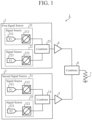
- FIG. 1 is a block diagram illustrating a configuration example of a low distortion amplifier 1 according to a first embodiment.
- the low distortion amplifier 1 includes a first signal source 2, a second signal source 3, a first amplifier 4, a second amplifier 5, an output combiner 6, and an output terminal 7, and compensates for an intermodulation distortion in a signal output from the output combiner 6.
- the first signal source 2 includes a signal source 21, a signal source 22, and a first input combiner 23, and an output signal of the first input combiner 23 is input to the first amplifier 4.
- the signal source 21 is a signal source that generates a first frequency F1 signal (fundamental wave signal having the first frequency F1), and includes a signal generating unit 211 and a first phase shifter 212.
- the signal source 22 is a signal source that generates a second frequency F2 signal (fundamental wave signal having the second frequency F2), and includes a signal generating unit 221 and a second phase shifter 222. Note that, in FIG. 1 and drawings described below, the input combiner and the output combiner are simply referred to as combiners for simplicity of illustration of the drawings.
- the second signal source 3 includes a signal source 31, a signal source 32, and a second input combiner 33, and an output signal of the second input combiner 33 is input to the second amplifier 5.
- the signal source 31 is a signal source that generates the first frequency F1 signal (fundamental wave signal having the first frequency F1), and includes a signal generating unit 311 and a first phase shifter 312.
- the signal source 32 is a signal source that generates the second frequency F2 signal (fundamental wave signal having the second frequency F2), and includes a signal generating unit 321 and a second phase shifter 322.
- DAC digital analog convertor
- DDS direct digital synthesize
- the signal source 21 and the signal source 31 operate in synchronization under control of a control unit (not illustrated), and a relationship in an amplitude and a phase between the first frequency F1 signal generated by the signal source 21 and the first frequency F1 signal generated by the signal source 31 is controlled.
- the signal source 22 and the signal source 32 operate in synchronization, and a relationship in an amplitude and a phase between the second frequency F2 signal generated by the signal source 22 and the second frequency F2 signal generated by the signal source 32 is controlled.
- FIG. 1 illustrates a case where the signal source 21 includes the signal generating unit 211 and the first phase shifter 212, the signal source 22 includes the signal generating unit 221 and the second phase shifter 222, the signal source 31 includes the signal generating unit 311 and the first phase shifter 312, and the signal source 32 includes the signal generating unit 321 and the second phase shifter 322, but it is not limited thereto.
- each of the signal source 21, the signal source 22, the signal source 31, and the signal source 32 may be a digital-to-analog converter such as a radio frequency digital to analog converter (RFDAC).
- RFDAC radio frequency digital to analog converter
- an output terminal of the first input combiner 23 is connected to an input terminal of the first amplifier 4, and a signal obtained by combining an output signal of the signal source 21 and an output signal of the signal source 22 is output to the first amplifier 4.
- a Wilkinson combiner is used as the first input combiner 23.
- the first input combiner 23 is not limited to an in-phase combiner, and may be a 90 degree hybrid combiner for different phase combination. In a case where the first input combiner 23 is the combiner, adjustment of different phases in the combiner may be required in a signal path on an input side or the like.
- the first amplifier 4 amplifies a signal output from the first signal source 2.
- An output terminal of the first amplifier 4 is connected to an input terminal of the first input combiner 23.
- the first amplifier 4 includes a field effect transistor (FET), a heterojunction bipolar transistor (HBT), or a high electron mobility transistor (HEMT), and a circuit including an input/output matching circuit and a bias circuit for the FET, the HBT, or the HEMT.
- FET field effect transistor
- HBT heterojunction bipolar transistor
- HEMT high electron mobility transistor
- an output terminal of the second input combiner 33 is connected to an input terminal of the second amplifier 5, and a signal obtained by combining an output signal of the signal source 31 and an output signal of the signal source 32 is output to the second amplifier 5.
- a Wilkinson combiner is used as the second input combiner 33.
- the second input combiner 33 is not limited to an in-phase combiner, and may be a 90 degree hybrid combiner for different phase combination. In a case where the second input combiner 33 is the combiner, adjustment of different phases in the combiner may be required in a signal path on an input side or the like.
- the second amplifier 5 amplifies a signal output from the second signal source 3.
- An output terminal of the second amplifier 5 is connected to an input terminal of the second input combiner 33.
- the second amplifier 5 includes an FET, an HBT, or an HEMT, and a circuit including an input/output matching circuit and a bias circuit for the FET, the HBT, or the HEMT.
- Gate biases of the first amplifier 4 and the second amplifier 5 have the same class of operation, but the class of operation is not limited.
- the first amplifier 4 and the second amplifier 5 are transistors under the same bias condition.
- the first amplifier 4 and the second amplifier 5 may be transistors having the same size.
- first amplifier 4 and the second amplifier 5 have the same electrical characteristics (output resistance and amplitude).
- the output combiner 6 is a combiner that combines a signal amplified by the first amplifier 4 and a signal amplified by the second amplifier 5.
- One of two input terminals included in the output combiner 6 is connected to the output terminal of the first amplifier 4, the other is connected to the output terminal of the second amplifier 5, and an output terminal of the output combiner 6 is connected to the output terminal 7.
- the output combiner 6 for example, a Wilkinson combiner or a 90 degree hybrid combiner is used.
- the output combiner 6 is not limited to an in-phase combiner, and may be a 90 degree hybrid combiner or the like for different phase combination. In a case where the output combiner 6 is the combiner, adjustment of different phases in the combiner may be required in a signal path on an input side or the like.
- the low distortion amplifier 1 is a so-called two-combining amplifier in which the output combiner 6 vector-combines a signal output from the first amplifier 4 and a signal output from the second amplifier 5 for each frequency, and outputs the resultant.
- Each of the signal output from the first amplifier 4 and the signal output from the second amplifier 5 includes an intermodulation distortion component having a frequency lower than the first frequency F1 and the second frequency F2 and an intermodulation distortion component having a frequency higher than the first frequency F1 and the second frequency F2 in addition to the first frequency F1 signal and the second frequency F2 signal which are fundamental wave signals.
- the low distortion amplifier 1 can switch an operation mode in which an intermodulation distortion component is cancelled by controlling a relationship between ⁇ F1 which is an angular difference in phase (hereinafter, simply referred to as a "phase difference") between the first frequency F1 signal input to the first amplifier 4 and the first frequency F1 signal input to the second amplifier 5 and a phase difference ⁇ F2 between the second frequency F2 signal input to the first amplifier 4 and the second frequency F2 signal input to the second amplifier 5.
- ⁇ F1 which is an angular difference in phase
- a first intermodulation distortion operation mode in which a low-frequency intermodulation wave distortion component and a high-frequency intermodulation distortion component are cancelled by performing control in such a manner that the phase difference ⁇ F1 between the first frequency F1 signals and the phase difference ⁇ F2 between the second frequency F2 signals are symmetrical.
- control is performed in such a manner that the phase difference ⁇ F1 between the first frequency F1 signals, the first frequency F1 being a center frequency, and the phase difference ⁇ F2 between the second frequency F2 signals, the second frequency F2 being a center frequency, are symmetrical depending on a frequency band.
- the symmetry indicates a relationship in which the magnitudes of the phase difference ⁇ F1 and the phase difference ⁇ F2 are within a range of values defined as being equal, and the phase difference ⁇ F1 and the phase difference ⁇ F2 have opposite polarities.
- the phase difference ⁇ F1 between the first frequency F1 signals satisfies the following equation (1)
- the phase difference ⁇ F2 between the second frequency F2 signals satisfies the following equation (2)
- X IM represents the order of an intermodulation distortion component.
- the following equation (1) is a relational equation indicating the phase difference ⁇ F1 necessary for canceling an intermodulation distortion component depending on the order of the intermodulation distortion component
- the following equation (2) is a relational equation indicating the phase difference ⁇ F2 necessary for canceling an intermodulation distortion component depending on the order of the intermodulation distortion component.
- FIG. 2 is a schematic diagram illustrating an outline of intermodulation distortion compensation in the first intermodulation distortion canceling operation mode.
- FIG. 3 is a graph illustrating a change in an output power waveform of the output combiner 6 in the first intermodulation distortion canceling operation mode.
- a graph on a left of an arrow indicates output power of the low distortion amplifier 1 before operation in the first intermodulation distortion canceling operation mode
- a graph on a right of the arrow indicates output power of the low distortion amplifier 1 operated in the first intermodulation distortion canceling operation mode.
- the low distortion amplifier 1 controls the phase difference ⁇ F1 and the phase difference ⁇ F2 between the first amplifier 4 and the second amplifier 5 in a symmetrical relationship depending on a frequency band. That is, the low distortion amplifier 1 performs control in such a manner that a relative relationship between the phase differences (the phase difference ⁇ F1 and the phase difference ⁇ F2 ) of input power depending on a frequency is symmetrical, whereby the operation mode is switched to the first intermodulation distortion canceling operation mode. At this time, an output power waveform of the output combiner 6 is switched from the graph on the left of the arrow to the graph on the right of the arrow.
- the first phase shifter 212 sets an angle of a phase of the first frequency F1 signal generated by the signal generating unit 211 to 30 degrees.
- the second phase shifter 222 sets an angle of a phase of the second frequency F2 signal generated by the signal generating unit 221 to -30 degrees.
- the first phase shifter 312 sets an angle of a phase of the first frequency F1 signal generated by the signal generating unit 311 to -30 degrees
- the second phase shifter 322 sets an angle of a phase of the second frequency F2 signal generated by the signal generating unit 321 to 30 degrees.
- the output combiner 6 combines a signal output from the first amplifier 4 and a signal output from the second amplifier 5.
- phase difference ⁇ F1 is 60 degrees and the phase difference ⁇ F2 is - 60 degrees, the phase difference ⁇ F1 and the phase difference ⁇ F2 are symmetrical.
- an amplitude of a signal generated by the first signal source 2 and an amplitude of a signal generated by the second signal source 3 are within a range of values defined to be equal.
- an RF component of each signal can be expressed by an equation of A ⁇ cos( ⁇ t + ⁇ ).
- A represents an amplitude
- t represents time
- ⁇ represents a phase.
- the first amplifier 4 receives a signal having a phase of 30 degrees of the first frequency F1 signal and a phase of -30 degrees of the second frequency F2 signal, and amplifies the input signal. At this time, as illustrated in FIG.
- the second amplifier 5 receives a signal having a phase of -30 degrees of the first frequency F1 signal and a phase of 30 degrees of the second frequency F2 signal. Since the phase difference ⁇ F1 between the first frequency F1 signal of the first amplifier 4 and the first frequency F1 signal of the second amplifier 5 is 60 degrees and the phase difference ⁇ F2 between the second frequency F2 signal of the first amplifier 4 and the second frequency F2 signal of the second amplifier 5 is -60 degrees, the phase difference ⁇ F1 and the phase difference ⁇ F2 are symmetrical.
- the order X IM of the intermodulation distortion is 3, and a sign described first is selected from the signs of 180 degrees (for example, in a case of +-180, +180 is selected.).
- the second amplifier 5 amplifies an input signal from the second signal source 3. At this time, as illustrated in FIG. 2 , due to nonlinearity of the second amplifier 5, in an output signal of the second amplifier 5, a third-order intermodulation distortion is generated, and a low-frequency intermodulation distortion component IM3' having a phase of -90 degrees and a high-frequency intermodulation distortion component IM3' having a phase of 90 degrees are included.
- the high-frequency third-order intermodulation distortion is also suppressed.
- the first phase shifter 212 sets the angle of the phase of the first frequency F1 signal to 30 degrees
- the first phase shifter 312 sets the angle of the phase of the first frequency F1 signal to -30 degrees.
- the low distortion amplifier 1 is not limited to these phases. That is, in a case where the third-order intermodulation distortion is generated, the phase difference ⁇ F1 between the first frequency F1 signals only needs to be 60 degrees.
- the second phase shifter 222 sets the angle of the phase of the second frequency F2 signal to -30 degrees
- second phase shifter 322 sets the angle of the phase of the second frequency F2 signal to 30 degrees.
- low distortion amplifier 1 is not limited to these phases. That is, in a case where the third-order intermodulation distortion is generated, the phase difference ⁇ F2 between the second frequency F2 signals only needs to be -60 degrees.
- the low distortion amplifier 1 allows an error of about 8% in phase.
- a fundamental wave signal included in the signal output from the first amplifier 4 and a fundamental wave signal included in the signal output from the second amplifier 5 are vector-combined by the output combiner 6.
- combining is performed in such a manner that a phase difference between the fundamental wave signal having the first frequency F1 output from the first amplifier 4 and the fundamental wave signal having the first frequency F1 output from the second amplifier 5 is 60 degrees.
- combining is performed in such a manner that a phase difference between the fundamental wave signal having the second frequency F2 output from the first amplifier 4 and the fundamental wave signal having the second frequency F2 output from the second amplifier 5 is -60 degrees.
- a low-frequency intermodulation distortion component and a high-frequency intermodulation distortion component are completely suppressed in an output signal of the output combiner 6, whereas an amplitude of the fundamental wave signal is about 87% of an amplitude of the input signal, and a power reduction amount of the fundamental wave signal with respect to the suppression amount of the intermodulation distortion is practically sufficient.
- control is performed in such a manner that an absolute value of the phase difference ⁇ F1 between the first frequency F1 signals, the first frequency F1 being a center frequency, and an absolute value of the phase difference ⁇ F2 between the second frequency F2 signals, the second frequency F2 being a center frequency, are equal to each other, and polarities thereof are opposite to each other depending on a frequency band.
- the phase difference ⁇ F1 between the first frequency F1 signal of the first amplifier 4 and the first frequency F1 signal of the second amplifier 5 is set to 60 degrees
- the phase difference ⁇ F2 between the second frequency F2 signal of the first amplifier 4 and the second frequency F2 signal of the second amplifier 5 is set to - 60 degrees
- control is performed in such a manner that the phase difference ⁇ F1 and the phase difference ⁇ F2 are symmetrical depending on a frequency band, whereby a relative relationship between amplitudes of third-order harmonics is controlled.
- control is performed in such a manner that the absolute value of the phase difference ⁇ F1 and the absolute value of the phase difference ⁇ F2 are equal to each other and polarities thereof are opposite to each other.
- the first amplifier 4 receives a signal in which the phase of the first frequency F1 signal is -30 degrees and the phase of the second frequency F2 signal is 30 degrees.
- a third-order intermodulation distortion is generated due to nonlinearity of amplification, and a low-frequency third-order intermodulation distortion component having a phase of -90 degrees and a high-frequency third-order intermodulation distortion component having a phase of 90 degrees are included.
- the second amplifier 5 receives a signal having a phase of 30 degrees of the first frequency F1 signal and a phase of -30 degrees of the second frequency F2 signal.
- the phase difference ⁇ F1 between the first frequency F1 signal of the first amplifier 4 and the first frequency F1 signal of the second amplifier 5 is -60 degrees
- the phase difference ⁇ F2 between the second frequency F2 signal of the first amplifier 4 and the second frequency F2 signal of the second amplifier 5 is 60 degrees
- the phase difference ⁇ F1 and the phase difference ⁇ F2 are symmetrical.
- the magnitudes of the phase differences for the first frequency F1 signal and the second frequency F2 signal satisfy the above equations (1) and (2), the order X IM of the intermodulation distortion is 3, and a sign described later is selected from the signs of 180 degrees (for example, in a case of +-180, -180 is selected.).
- the second amplifier 5 amplifies an input signal from the second signal source 3. At this time, due to nonlinearity of the second amplifier 5, in an output signal of the second amplifier 5, a third-order intermodulation distortion is generated, and a low-frequency intermodulation distortion component having a phase of 90 degrees and a high-frequency intermodulation distortion component having a phase of -90 degrees are included.
- the first phase shifter 212 sets the angle of the phase of the first frequency F1 signal to -30 degrees
- the first phase shifter 312 sets the angle of the phase of the first frequency F1 signal to 30 degrees.
- the low distortion amplifier 1 is not limited to these phases. That is, in a case where the third-order intermodulation distortion is generated, the phase difference ⁇ F1 between the first frequency F1 signals only needs to be -60 degrees.
- the second phase shifter 222 sets the angle of the phase of the second frequency F2 signal to 30 degrees
- second phase shifter 322 sets the angle of the phase of the second frequency F2 signal to -30 degrees.
- low distortion amplifier 1 is not limited to these phases. That is, in a case where the third-order intermodulation distortion is generated, the phase difference ⁇ F2 between the second frequency F2 signals only needs to be 60 degrees.
- the low distortion amplifier 1 allows an error of about 8% in phase.
- a fundamental wave signal included in the signal output from the first amplifier 4 and a fundamental wave signal included in the signal output from the second amplifier 5 are vector-combined by the output combiner 6.
- combining is performed in such a manner that a phase difference between the fundamental wave signal having the first frequency F1 output from the first amplifier 4 and the fundamental wave signal having the first frequency F1 output from the second amplifier 5 is -60 degrees.
- combining is performed in such a manner that a phase difference between the fundamental wave signal having the second frequency F2 output from the first amplifier 4 and the fundamental wave signal having the second frequency F2 output from the second amplifier 5 is 60 degrees.
- a low-frequency intermodulation distortion component and a high-frequency intermodulation distortion component are completely suppressed in an output signal of the output combiner 6, whereas an amplitude of the fundamental wave signal is about 87% of an amplitude of the input signal, and a power reduction amount of the fundamental wave signal with respect to the suppression amount of the intermodulation distortion is practically sufficient.
- the phase difference ⁇ F1 between the first frequency F1 signal of the first amplifier 4 and the first frequency F1 signal of the second amplifier 5 is +-60 degrees
- the phase difference ⁇ F2 between the second frequency signal of the first amplifier 4 and the second frequency signal of the second amplifier 5 is -+60 degrees depending on a frequency band
- the magnitudes of ⁇ F1 and ⁇ F2 satisfy the above equations (1) and (2)
- X IM is 3.
- control is performed in such a manner that the magnitude of the phase difference ⁇ F1 between the first frequency F1 signal of the first amplifier 4 and the first frequency F1 signal of the second amplifier 5 and the magnitude of the phase difference ⁇ F2 between the second frequency signal of the first amplifier 4 and the second frequency signal of the second amplifier 5 satisfy the above equations (1) and (2), and the phase difference ⁇ F1 and the phase difference ⁇ F2 are symmetrical, whereby the intermodulation distortion is canceled.
- control is performed in such a manner that the magnitude of the phase difference ⁇ F1 between the first frequency F1 signal of the first amplifier 4 and the first frequency F1 signal of the second amplifier 5 and the magnitude of the phase difference ⁇ F2 between the second frequency F2 signal of the first amplifier 4 and the second frequency F2 signal of the second amplifier 5 are each 26 degrees and satisfy the above equations (1) and (2), X IM is 5, and the phase difference ⁇ F1 and the phase difference ⁇ F2 are symmetrical, whereby a relative relationship between amplitudes of fifth-order harmonics can be controlled.
- the low distortion amplifier 1 can suppress an intermodulation distortion while suppressing deterioration of a fundamental wave signal by performing control in such a manner that the phase difference ⁇ F1 and the phase difference ⁇ F2 are symmetrical.
- the degree of freedom for band selection is high, and it is possible to cancel intermodulation distortions of any different orders for a low-frequency intermodulation distortion and a high-frequency intermodulation distortion.
- Equation (3) represents the phase difference ⁇ F1 between the low-frequency first frequency F1 signal of the first amplifier 4 and the low-frequency first frequency F1 signal of the second amplifier 5
- equation (4) represents the phase difference ⁇ F2 between the high-frequency second frequency F2 signal of the first amplifier 4 and the high-frequency second frequency F2 signal of the second amplifier 5.
- Y IML represents the order of a low-frequency intermodulation distortion component.
- Z IMH represents the order of a high-frequency intermodulation distortion component.
- the low distortion amplifier 1 performs control in such a manner that the magnitude of the phase difference ⁇ F1 between the first frequency F1 signals satisfies the above equation (3) and the magnitude of the phase difference ⁇ F2 between the second frequency F2 signals satisfies the above equation (4) depending on a frequency band, whereby the first intermodulation distortion canceling operation mode is switched to the second intermodulation distortion operation mode, and it is possible to cancel intermodulation distortions of any different orders.
- FIG. 4 is a schematic diagram illustrating an outline of intermodulation distortion compensation in the second intermodulation distortion canceling operation mode.
- FIG. 5 is a graph illustrating a change in an output power waveform of the output combiner 6 in the second intermodulation distortion canceling operation mode.
- a graph on a left of an arrow indicates output power of the low distortion amplifier 1 before operation in the second intermodulation distortion canceling operation mode
- a graph on a right of the arrow indicates output power of the low distortion amplifier 1 operated in the second intermodulation distortion canceling operation mode.
- FIG. 4 and 5 illustrate a case where, for example, an intermodulation distortion component IM3 which is a high-frequency third-order harmonic and an intermodulation distortion component IM7 which is a low-frequency seventh-order harmonic are canceled in the second intermodulation distortion canceling operation mode.
- PB represents a pass band of a filter
- IM represents an intermodulation distortion generated around a cutoff frequency band of the filter.
- the low distortion amplifier 1 removes the intermodulation distortion depending on a cutoff frequency of the filter. Furthermore, the low distortion amplifier 1 performs control in such a manner that the magnitudes of the phase differences (the phase difference ⁇ F1 and the phase difference A ⁇ F2 ) of input power depending on a frequency satisfy the above equations (3) and (4), whereby the operation mode is switched to the second intermodulation distortion canceling operation mode. At this time, an output power waveform of the output combiner 6 is switched from the graph on the left of the arrow to the graph on the right of the arrow.
- the first phase shifter 212 sets an angle of a phase of the first frequency F1 signal generated by the signal generating unit 211 to 18 degrees.
- the second phase shifter 222 sets an angle of a phase of the second frequency F2 signal generated by the signal generating unit 221 to 54 degrees.
- the first phase shifter 312 sets an angle of a phase of the first frequency F1 signal generated by the signal generating unit 311 to -18 degrees
- the second phase shifter 322 sets an angle of a phase of the second frequency F2 signal generated by the signal generating unit 321 to -54 degrees.
- the output combiner 6 combines a signal output from the first amplifier 4 and a signal output from the second amplifier 5.
- phase difference ⁇ F1 is 36 degrees and the phase difference ⁇ F2 is 108 degrees, the phase difference ⁇ F1 and the phase difference ⁇ F2 satisfy the above equations (3) and (4).
- the first amplifier 4 receives a combined signal having a phase of 18 degrees of the first frequency F1 signal and a phase of 54 degrees of the second frequency F2 signal, and amplifies the input signal. At this time, due to nonlinearity of the first amplifier 4, a third-order intermodulation distortion and a seventh-order intermodulation distortion are generated in an output signal of the first amplifier 4. As a result, as illustrated in FIG.
- a low-frequency third-order intermodulation distortion component having a phase of -18 degrees and a high-frequency third-order intermodulation distortion component having a phase of 90 degrees are included as a third-order intermodulation distortion component IM3
- a low-frequency seventh-order intermodulation distortion component having a phase of -90 degrees and a high-frequency seventh-order intermodulation distortion component having a phase of 162 degrees are included as a seventh-order intermodulation distortion component IM7.
- the second amplifier 5 receives a signal having a phase of -18 degrees of the first frequency F1 signal and a phase of -54 degrees of the second frequency F2 signal.
- the phase difference ⁇ F1 between the first frequency F1 signal of the first amplifier 4 and the first frequency F1 signal of the second amplifier 5 is 36 degrees
- the phase difference ⁇ F2 between the second frequency F2 signal of the first amplifier 4 and the second frequency F2 signal of the second amplifier 5 is 108 degrees.
- the magnitudes of the phase differences for the first frequency F1 and the second frequency F2 satisfy the above equations (3) and (4), the order Y IML of the low-frequency intermodulation distortion is 7, the order Z IMH of the high-frequency intermodulation distortion is 3, and a sign described later is selected from the signs of 180 degrees (for example, in a case of +-180, -180 is selected.). Since the above equations (3) and (4) include the above equations (1) and (2), the relationship between the phase difference ⁇ F1 and the phase difference ⁇ F2 is more generally controlled than in the first intermodulation distortion canceling operation mode.
- the second amplifier 5 amplifies an input signal from the second signal source 3. At this time, due to nonlinearity of the second amplifier 5, a third-order intermodulation distortion and a seventh-order intermodulation distortion are generated in an output signal of the second amplifier 5.
- a low-frequency third-order intermodulation distortion component having a phase of 18 degrees and a high-frequency third-order intermodulation distortion component having a phase of -90 degrees are included as a third-order intermodulation distortion component IM3'
- a low-frequency seventh-order intermodulation distortion component having a phase of 90 degrees and a high-frequency seventh-order intermodulation distortion component having a phase of -162 degrees are included as a seventh-order intermodulation distortion component IM7'.
- the first phase shifter 212 sets the angle of the phase of the first frequency F1 signal to 18 degrees
- the first phase shifter 312 sets the angle of the phase of the first frequency F1 signal to -18 degrees.
- the low distortion amplifier 1 is not limited to these phases. That is, in a case where the intermodulation distortion is generated, the phase difference ⁇ F1 between the first frequency F1 signals only needs to be 36 degrees.
- the phase of the first frequency F1 signal input to the first amplifier 4 may be set to 36 degrees
- the phase of the first frequency F1 signal input to the second amplifier 5 may be set to 0 degrees.
- the second phase shifter 222 sets the angle of the phase of the second frequency F2 signal to 54 degrees
- second phase shifter 322 sets the angle of the phase of the second frequency F2 signal to -54 degrees.
- low distortion amplifier 1 is not limited to these phases. That is, in a case where the intermodulation distortion is generated, the phase difference ⁇ F2 between the second frequency F2 signals only needs to be 108 degrees.
- the phase of the second frequency F2 signal input to the first amplifier 4 may be set to 108 degrees
- the phase of the second frequency F2 signal input to the second amplifier 5 may be set to 0 degrees.
- the output combiner 6 vector-combines the input signals, whereby the phase difference ⁇ F1 between the fundamental wave signal having the first frequency F1 of the first amplifier 4 and the fundamental wave signal having the first frequency F1 of the second amplifier 5 is combined at 36 degrees, and the phase difference ⁇ F2 between the fundamental wave signal having the second frequency F2 of the first amplifier 4 and the fundamental wave signal having the second frequency F2 of the second amplifier 5 is combined at 108 degrees.
- the low-frequency seventh-order intermodulation distortion and the high-frequency third-order intermodulation distortion are completely suppressed, whereas a power reduction amount of the fundamental wave signal is practically sufficient.
- the low distortion amplifier 1 can cancel any different intermodulation distortions other than the low-frequency third-order harmonic and the high-frequency seventh harmonic.
- the low distortion amplifier 1 can control a relative relationship between an amplitude of a fifth-order harmonic and an amplitude of a seventh-order harmonic, and can cancel the low-frequency fifth-order harmonic and the high-frequency seventh-order harmonic.
- control is performed in such a manner that the phase difference ⁇ F1 and the phase difference ⁇ F2 satisfy the above equations (3) and (4) by setting the phase difference ⁇ F1 to 60 degrees and setting the phase difference ⁇ F2 to 0 degrees, Y IML is 5, and Z IMH is 7, whereby a relative relationship between an amplitude of the fifth-order harmonic and an amplitude of the seventh-order harmonic can be controlled.
- the second intermodulation distortion canceling operation mode Since intermodulation distortions of different orders can be cancelled in the second intermodulation distortion canceling operation mode, for example, as illustrated in FIG. 5 , intermodulation distortions in a cutoff band of a filter can be canceled. As a result, a frequency band in which a distortion is compensated can be enlarged without enlarging a pass band of the filter, and the wideband low distortion amplifier 1 is achieved.
- the low distortion amplifier 1 operating in the second intermodulation distortion canceling operation mode can perform distortion compensation in which a ratio at which the intermodulation distortion component is suppressed is larger than a ratio at which the fundamental wave signal is deteriorated.
- the degree of freedom for band selection is high, and it is possible to cancel intermodulation distortions of any different orders for a low-frequency intermodulation distortion or a high-frequency intermodulation distortion. That is, in the third intermodulation distortion canceling operation mode, it is possible to cancel only one of the low-frequency intermodulation distortion and the high-frequency intermodulation distortion.
- the following equation (5) represents a relationship between the phase difference ⁇ F1 between the first frequency F1 signal of the first amplifier 4 and the first frequency F1 signal of the second amplifier 5, and the phase difference ⁇ F2 between the second frequency F2 signal of the first amplifier 4 and the second frequency F2 signal of the second amplifier 5 in the high-frequency intermodulation distortion.
- the following equation (6) represents a relationship between the phase difference ⁇ F1 between the first frequency F1 signal of the first amplifier 4 and the first frequency F1 signal of the second amplifier 5, and the phase difference ⁇ F2 between the second frequency F2 signal of the first amplifier 4 and the second frequency F2 signal of the second amplifier 5 in the low-frequency intermodulation distortion.
- n and m are integers.
- the low distortion amplifier 1 performs control in such a manner that the magnitude of the phase difference ⁇ F1 between the first frequency F1 signals and the magnitude of the phase difference ⁇ F2 between the second frequency F2 signals satisfy the above equation (5) depending on a frequency band, whereby the operation mode is switched to the third intermodulation distortion operation mode.
- the third intermodulation distortion operation mode it is possible to cancel intermodulation distortion of any order and any band.
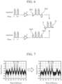
- FIG. 6 is a schematic diagram illustrating an outline of intermodulation distortion compensation in the third intermodulation distortion canceling operation mode.
- FIG. 7 is a graph illustrating a change in an output power waveform of the output combiner 6 in the third intermodulation distortion canceling operation mode.
- a graph on a left of an arrow indicates output power of the low distortion amplifier 1 before operation in the third intermodulation distortion canceling operation mode
- a graph on a right of the arrow indicates output power of the low distortion amplifier 1 operated in the third intermodulation distortion canceling operation mode.
- FIGS. 6 and 7 illustrate a case where, for example, an intermodulation distortion component IM3 which is a high-frequency third-order harmonic is canceled in the third intermodulation distortion canceling operation mode.
- the low distortion amplifier 1 performs control in such a manner that the magnitudes of the phase differences (the phase difference ⁇ F1 and the phase difference ⁇ F2 ) of input power depending on a frequency satisfy the above equation (5), whereby the operation mode is switched to the third intermodulation distortion canceling operation mode.
- an output power waveform of the output combiner 6 is switched from the graph on the left of the arrow to the graph on the right of the arrow.
- the first phase shifter 212 sets an angle of a phase of the first frequency F1 signal generated by the signal generating unit 211 to 0 degrees.
- the second phase shifter 222 sets an angle of a phase of the second frequency F2 signal generated by the signal generating unit 221 to 90 degrees.
- the first phase shifter 312 sets an angle of a phase of the first frequency F1 signal generated by the signal generating unit 311 to 0 degrees
- the second phase shifter 322 sets an angle of a phase of the second frequency F2 signal generated by the signal generating unit 321 to 0 degrees.
- the output combiner 6 combines a signal output from the first amplifier 4 and a signal output from the second amplifier 5.
- the first amplifier 4 receives a signal having a phase of 0 degrees of the first frequency F1 signal and a phase of 90 degrees of the second frequency F2 signal, and amplifies the input signal. At this time, due to nonlinearity of the first amplifier 4, a third-order intermodulation distortion is generated in an output signal of the first amplifier 4. As a result, in the output signal of the first amplifier 4, as illustrated in FIG. 6 , a low-frequency third-order intermodulation distortion component having a phase of -90 degrees and a high-frequency third-order intermodulation distortion component having a phase of 180 degrees are included as a third-order intermodulation distortion component IM3.
- the second amplifier 5 receives a signal having a phase of 0 degrees of the first frequency F1 signal and a phase of 0 degrees of the second frequency F2 signal.
- the phase difference ⁇ F1 between the first frequency F1 signal of the first amplifier 4 and the first frequency F1 signal of the second amplifier 5 is 0 degrees
- the phase difference ⁇ F2 between the second frequency F2 signal of the first amplifier 4 and the second frequency F2 signal of the second amplifier 5 is 90 degrees.
- the magnitudes of the phase differences for the first frequency F1 and the second frequency F2 satisfy the above equation (5), n is 1, and a sign of + is selected from the signs of 180 degrees (for example, in a case of +-180, +180 is selected.). Since the above equations (5) and (6) include the above equations (3) and (4), the relationship between the phase difference ⁇ F1 and the phase difference ⁇ F2 is more generally controlled than in the second intermodulation distortion canceling operation mode.
- the second amplifier 5 amplifies an input signal from the second signal source 3. At this time, due to nonlinearity of the second amplifier 5, a third-order intermodulation distortion and a seventh-order intermodulation distortion are generated in an output signal of the second amplifier 5. As a result, in the output signal of the second amplifier 5, a low-frequency third-order intermodulation distortion component having a phase of 0 degrees and a high-frequency third-order intermodulation distortion component having a phase of 0 degrees are included as a third-order intermodulation distortion component IM3'.
- the high-frequency third-order intermodulation distortion is suppressed.
- the first phase shifter 212 sets the angle of the phase of the first frequency F1 signal to 0 degrees
- the first phase shifter 312 sets the angle of the phase of the first frequency F1 signal to 0 degrees.
- the low distortion amplifier 1 is not limited to these phases. That is, in a case where the intermodulation distortion is generated, the phase difference ⁇ F1 between the first frequency F1 signals only needs to be 0 degrees.
- phase of the first frequency F1 signal input to the first amplifier 4 may be set to 60 degrees
- the phase of the first frequency F1 signal input to the second amplifier 5 may be set to 60 degrees
- the second phase shifter 222 sets the angle of the phase of the second frequency F2 signal to 90 degrees
- second phase shifter 322 sets the angle of the phase of the second frequency F2 signal to 0 degrees.
- low distortion amplifier 1 is not limited to these phases. That is, in a case where the intermodulation distortion is generated, the phase difference ⁇ F2 between the second frequency F2 signals only needs to be 90 degrees.
- the phase of the second frequency F2 signal input to the first amplifier 4 may be set to 100 degrees
- the phase of the second frequency F2 signal input to the second amplifier 5 may be set to 10 degrees.
- the output combiner 6 vector-combines the input signals, whereby the phase difference ⁇ F1 between the fundamental wave signal having the first frequency F1 of the first amplifier 4 and the fundamental wave signal having the first frequency F1 of the second amplifier 5 is combined at 0 degrees, and the phase difference ⁇ F2 between the fundamental wave signal having the second frequency F2 of the first amplifier 4 and the fundamental wave signal having the second frequency F2 of the second amplifier 5 is combined at 90 degrees.
- the phase difference ⁇ F1 between the fundamental wave signal having the first frequency F1 of the first amplifier 4 and the fundamental wave signal having the first frequency F1 of the second amplifier 5 is combined at 0 degrees
- the phase difference ⁇ F2 between the fundamental wave signal having the second frequency F2 of the first amplifier 4 and the fundamental wave signal having the second frequency F2 of the second amplifier 5 is combined at 90 degrees.
- the low distortion amplifier 1 can cancel the low-frequency third-order intermodulation distortion.
- the low distortion amplifier 1 can control a relative relationship between amplitudes of third-order harmonics, and can cancel the low-frequency third-order harmonic.
- the low distortion amplifier 1 can perform distortion compensation in which a ratio at which the intermodulation distortion component is suppressed is larger than a ratio at which the fundamental wave signal is deteriorated.
- the low distortion amplifier 1 operates in an operation mode in which the phase difference ⁇ F1 between the first frequency F1 signals input to the first amplifier 4 and the second amplifier 5 and the phase difference ⁇ F2 between the second frequency F2 signals input to the first amplifier 4 and the second amplifier 5 satisfy a relational equation in which an intermodulation distortion component included in the signal amplified by the first amplifier 4 and an intermodulation distortion component included in the signal amplified by the second amplifier 5 are in opposite phases.
- the low distortion amplifier 1 can perform distortion compensation in which a ratio at which the intermodulation distortion component is suppressed is larger than a ratio at which a fundamental wave signal is deteriorated.
- the low distortion amplifier 1 operates in the third intermodulation distortion canceling operation mode, and can perform distortion compensation in which a ratio at which the intermodulation distortion component is suppressed is larger than a ratio at which the fundamental wave signal is deteriorated.
- the low distortion amplifier 1 operates in the second intermodulation distortion canceling operation mode, and can perform distortion compensation in which a ratio at which the intermodulation distortion component is suppressed is larger than a ratio at which the fundamental wave signal is deteriorated.
- the low distortion amplifier 1 operates in the first intermodulation distortion canceling operation mode, and can perform distortion compensation in which a ratio at which the intermodulation distortion component is suppressed is larger than a ratio at which the fundamental wave signal is deteriorated.
- the first amplifier 4 and the second amplifier 5 are transistors having the same size.
- the first amplifier 4 and the second amplifier 5 are transistors under the same bias condition.
- FIG. 8 is a block diagram illustrating a configuration example of a low distortion amplifier 1A according to a second embodiment.
- the low distortion amplifier 1A can operate in first to third intermodulation distortion canceling operation modes and includes a first signal source 2A, a second signal source 3A, a first amplifier 4, a second amplifier 5, an output combiner 6, and an output terminal 7.
- the first signal source 2A includes a signal source 21A that generates a first frequency F1 signal (fundamental wave signal having the first frequency F1), a signal source 22A that generates a second frequency F2 signal (fundamental wave signal having the second frequency F2), and a first input combiner 23.
- the second signal source 3A includes a signal source 31A that generates a first frequency F1 signal (fundamental wave signal having the first frequency F1), a signal source 32A that generates a second frequency F2 signal (fundamental wave signal having the second frequency F2), and a second input combiner 33.
- an RFDAC may be used as each of the signal source 21A, the signal source 22A, the signal source 31A, and the signal source 32A.
- the signal source 21A and the signal source 31A operate in synchronization under control of a control unit (not illustrated), and a relationship in an amplitude and a phase between the first frequency F1 signal generated by the signal source 21A and the first frequency F1 signal generated by the signal source 31A is controlled.
- the signal source 22A and the signal source 32A operate in synchronization, and a relationship in an amplitude and a phase between the second frequency F2 signal generated by the signal source 22A and the second frequency F2 signal generated by the signal source 32A is controlled.
- FIG. 9 is a block diagram illustrating a configuration of a low distortion amplifier 1B that is a modification of the low distortion amplifier 1A.
- the low distortion amplifier 1B includes a first signal source 2B, a second signal source 3B, the first amplifier 4, the second amplifier 5, the output combiner 6, and the output terminal 7, and each of the first signal source 2B and the second signal source 3B is constituted by an RFDAC.
- each of the signal source 21A, the signal source 22A, the signal source 31A, and the signal source 32A is an RFDAC.
- each of the first signal source 2B and the second signal source 3B is an RFDAC.
- FIG. 10 is a block diagram illustrating a configuration example of a low distortion amplifier 1C according to a third embodiment.
- the low distortion amplifier 1C achieves low distortion compensation and widening of a band of two modulated waves without using a feedback reception system.
- the low distortion amplifier 1C includes a first signal source 2C, a second signal source 3C, a first amplifier 4, a second amplifier 5, an output combiner 6, an output terminal 7, and a distortion compensation circuit 8.
- the first signal source 2C generates a signal to be input to the first amplifier 4.
- the signal to be input to the first amplifier 4 includes a first frequency F1 signal (fundamental wave signal having the first frequency F1) and a second frequency F2 signal (fundamental wave signal having the second frequency F2).
- the second signal source 3C generates a signal to be input to the second amplifier 5.
- the signal to be input to the second amplifier 5 includes a first frequency F1 signal (fundamental wave signal having the first frequency F1) and a second frequency F2 signal (fundamental wave signal having the second frequency F2).
- an RFDAC is used as each of the first signal source 2C and the second signal source 3C.
- the first signal source 2C and the second signal source 3C operate in synchronization under control of a control unit (not illustrated), and a relationship in an amplitude and a phase between the first frequency F1 signal generated by the first signal source 2C and the first frequency F1 signal generated by the second signal source 3C is controlled. Similarly, a relationship in an amplitude and a phase between the second frequency F2 signal generated by the first signal source 2C and the second frequency F2 signal generated by the second signal source 3C is controlled.
- the distortion compensation circuit 8 is a circuit that extracts, as a distortion, a difference between a theoretical value and an actual measurement value of an output signal of the first amplifier 4 in such a manner that a relationship between an input signal and the output signal of the first amplifier 4 is linear depending on a frequency band, and adds signal information that compensates for the distortion to the input signal.
- An input terminal of the distortion compensation circuit 8 is connected to an input terminal and an output terminal of the first amplifier 4, and an output terminal of the distortion compensation circuit 8 is connected to the first signal source 2C and the second signal source 3C.
- the first signal source 2C and the second signal source 3C operate in synchronization, and amplitudes of the fundamental wave signals generated by the first signal source 2C and the second signal source 3C are equal to each other. Therefore, a distortion of a signal generated when the input signal is amplified through the first amplifier 4, extracted from the input signal and the output signal of the first amplifier 4 by the distortion compensation circuit 8 and signal information that compensates for the distortion can be included in each of a signal generated by the first signal source 2C and a signal generated by the second signal source 3C.
- a digital pre-distortion (DPD) is used as the distortion compensation circuit 8.
- the low distortion amplifier 1C includes the distortion compensation circuit 8 that adds, to a signal generated by the first signal source 2C and output to the first amplifier 4 and a signal generated by the second signal source 3C and output to the second amplifier 5, signal information that compensates for distortions generated in the signals.
- the distortion compensation circuit 8 can achieve low distortion compensation and widening of a band of two modulated waves without using a feedback reception system.
- the output combiner 6 is an analog circuit that combines a signal output from the first amplifier 4 and a signal output from the second amplifier 5 has been described, but it is not limited thereto.
- the output combiner 6 may emit a signal output from the first amplifier 4 into space and may emit a signal output from the second amplifier 5 into space, thereby vector-combining these signals in space.
- FIG. 11 is a block diagram illustrating a configuration of a low distortion amplifier 1D that is a modification of the low distortion amplifiers according to the first to third embodiments.
- the low distortion amplifier 1D includes a first signal source 2D, a second signal source 3D, the first amplifier 4, the second amplifier 5, the output combiner 6, a first signal emitter 9A, and a second signal emitter 9B.
- the first signal source 2D is a signal source that generates a signal to be emitted from the first signal emitter 3D2, and includes a signal generating unit 2D1 and a phase shifter 2D2.
- the signal generating unit 2D1 operates similarly to the RFDAC illustrated in FIGS. 9 and 10 .
- the phase shifter 2D2 operates similarly to the phase shifters 212, 222, 312, and 322 illustrated in FIG. 1 .
- the second signal source 3D is a signal source that generates a signal to be emitted from the second signal emitter 9B, and includes a signal generating unit 3D1 and a phase shifter 3D2. Note that the signal generating unit 3D1 operates similarly to the RFDAC illustrated in FIGS. 9 and 10 . In addition, the phase shifter 3D2 operates similarly to the phase shifters 212, 222, 312, and 322 illustrated in FIG. 1 .
- a signal output from the first amplifier 4 is emitted into space as a first emission signal by the first signal emitter 9A
- a signal output from the second amplifier 5 is emitted into space as a second emission signal by the second signal emitter 9B.
- the angle of a beam array formed by the first signal emitter 9A is ⁇ F1
- the first signal emitter 9A emits the first emission signal having the phase difference ⁇ F1
- the angle of a beam array formed by the second signal emitter 9B is ⁇ F2
- the second signal emitter 9B emits a second emission signal having the phase difference ⁇ F2 .
- the output combiner 6 vector-combines the first emission signal and the second emission signal in space.
- a circuit that inputs a signal to each of the first amplifier 4 and the second amplifier 5 a circuit illustrated in any one of FIGS. 1 and 8 to 10 illustrated in the first to third embodiments may be used.
- the low distortion amplifier 1D configured to vector-combine a signal amplified by the first amplifier 4 and a signal amplified by the second amplifier 5 in space can obtain similar effects to those of the above-described first to third embodiments.
- the low distortion amplifier according to the present disclosure can be used, for example, for mobile object communication.
- 1, 1A, 1B, 1C, 1D low distortion amplifier
- 2, 2A, 2B, 2C, 2D first signal source
- 3, 3A, 3B, 3C, 3D second signal source
- 2D2, 3D2 phase shifter
- 9B second signal emitter
- 21, 21A, 22, 22A, 31, 31A, 32, 32A signal source
- 23 first input combiner
- 211, 2D1, 3D1 signal generating unit
- 212, 312 first phase shifter
- 221, 311, 321 signal generating unit
Landscapes
- Engineering & Computer Science (AREA)
- Power Engineering (AREA)
- Physics & Mathematics (AREA)
- Nonlinear Science (AREA)
- Amplifiers (AREA)
Abstract
Description
- The present disclosure relates to a low distortion amplifier.
- In recent years, one amplifier for a fifth or sixth generation mobile communication base station is required to be applicable to a plurality of bands and to operate in an ultra-wide band in order to be used in large-capacity communication. Note that an amplifier operating with two modulated waves generates an intermodulation distortion between the modulated waves, and thus, it is necessary to reduce the intermodulation distortion. When an intermodulation distortion between modulated waves is generated, a band obtained by combining a low frequency side and a high frequency side is wider than a band of a generally widespread transceiver, and therefore digital distortion compensation (spurious suppression) cannot be applied.
- For example, an amplifier circuit disclosed in Patent Literature 1 divides input signals of two modulated waves into a normal phase and a reverse phase, inputs the signals having phases different from each other to a first amplifier and a second amplifier, and combines input signals amplified by the first amplifier and the second amplifier. As a result, a signal (intermodulation distortion) of a frequency component generated by an intermodulation distortion, included in the output signal (fundamental wave) of the first amplifier is suppressed by a signal (intermodulation distortion) of a reverse characteristic in the frequency component, included in the output signal (fundamental wave) of the second amplifier.
- Patent Literature 1:
JP 2007-243491 A - In the conventional technique disclosed in Patent Literature 1, with an amplitude difference between a fundamental wave signal output from the first amplifier and a fundamental wave signal output from the second amplifier, a ratio at which the fundamental wave signal is canceled is reduced as compared with an intermodulation distortion component in combining signals on an output side. However, this method has a problem that although power of the intermodulation distortion component with respect to power of the fundamental wave signal is reduced, the power of the fundamental wave signal is largely lost, and a highly efficient operation cannot be performed.
- The present disclosure has been made in order to solve the above problems, and an object of the present disclosure is to obtain a low distortion amplifier capable of performing distortion compensation in which a ratio at which an intermodulation distortion component is suppressed is larger than a ratio at which a fundamental wave signal is deteriorated.
- A low distortion amplifier according to the present disclosure includes: a first signal source that outputs a signal obtained by combining a first frequency signal and a second frequency signal, the second frequency being different from the first frequency; a second signal source that outputs a signal obtained by combining the first frequency signal and the second frequency signal; a first amplifier that receives the signal output from the first signal source and amplifies the input signal; a second amplifier that receives the signal output from the second signal source and amplifies the input signal; and a combiner that combines the signal amplified by the first amplifier and the signal amplified by the second amplifier, and operates in an operation mode in which a phase difference between the first frequency signals input to the first amplifier and the second amplifier and a phase difference between the second frequency signals input to the first amplifier and the second amplifier satisfy a relational equation in which an intermodulation distortion component included in the signal amplified by the first amplifier and an intermodulation distortion component included in the signal amplified by the second amplifier are in opposite phases.
- According to the present disclosure, an operation is performed in an operation mode in which a phase difference between the first frequency signals input to the first amplifier and the second amplifier and a phase difference between the second frequency signals input to the first amplifier and the second amplifier satisfy a relational equation in which an intermodulation distortion component included in the signal amplified by the first amplifier and an intermodulation distortion component included in the signal amplified by the second amplifier are in opposite phases. As a result, when the signal amplified by the first amplifier and the signal amplified by the second amplifier are combined, only the intermodulation distortion components included in these signals are combined in opposite phases, and therefore the low distortion amplifier according to the present disclosure can perform distortion compensation in which a ratio at which the intermodulation distortion component is suppressed is larger than a ratio at which a fundamental wave signal is deteriorated.
-
-
FIG. 1 is a block diagram illustrating a configuration example of a low distortion amplifier according to a first embodiment. -
FIG. 2 is a schematic diagram illustrating an outline of intermodulation distortion compensation in a first intermodulation distortion canceling operation mode. -
FIG. 3 is a graph illustrating a change in an output power waveform of an output combiner in the first intermodulation distortion canceling operation mode. -
FIG. 4 is a schematic diagram illustrating an outline of intermodulation distortion compensation in a second intermodulation distortion canceling operation mode. -
FIG. 5 is a graph illustrating a change in an output power waveform of an output combiner in the second intermodulation distortion canceling operation mode. -
FIG. 6 is a schematic diagram illustrating an outline of intermodulation distortion compensation in a third intermodulation distortion canceling operation mode. -
FIG. 7 is a graph illustrating a change in an output power waveform of an output combiner in the third intermodulation distortion canceling operation mode. -
FIG. 8 is a block diagram illustrating a configuration example of a low distortion amplifier according to a second embodiment. -
FIG. 9 is a block diagram illustrating a configuration of a modification of the low distortion amplifier according to the second embodiment. -
FIG. 10 is a block diagram illustrating a configuration example of a low distortion amplifier according to a third embodiment. -
FIG. 11 is a block diagram illustrating a configuration of a modification of the low distortion amplifiers according to the first to third embodiments. -
FIG. 1 is a block diagram illustrating a configuration example of a low distortion amplifier 1 according to a first embodiment. InFIG. 1 , the low distortion amplifier 1 includes a first signal source 2, a second signal source 3, a first amplifier 4, a second amplifier 5, an output combiner 6, and anoutput terminal 7, and compensates for an intermodulation distortion in a signal output from the output combiner 6. The first signal source 2 includes asignal source 21, asignal source 22, and a first input combiner 23, and an output signal of thefirst input combiner 23 is input to the first amplifier 4. Thesignal source 21 is a signal source that generates a first frequency F1 signal (fundamental wave signal having the first frequency F1), and includes asignal generating unit 211 and afirst phase shifter 212. Thesignal source 22 is a signal source that generates a second frequency F2 signal (fundamental wave signal having the second frequency F2), and includes asignal generating unit 221 and asecond phase shifter 222. Note that, inFIG. 1 and drawings described below, the input combiner and the output combiner are simply referred to as combiners for simplicity of illustration of the drawings. - The second signal source 3 includes a
signal source 31, asignal source 32, and a second input combiner 33, and an output signal of thesecond input combiner 33 is input to the second amplifier 5. Thesignal source 31 is a signal source that generates the first frequency F1 signal (fundamental wave signal having the first frequency F1), and includes asignal generating unit 311 and afirst phase shifter 312. Thesignal source 32 is a signal source that generates the second frequency F2 signal (fundamental wave signal having the second frequency F2), and includes asignal generating unit 321 and asecond phase shifter 322. For each of thesignal generating unit 211, thesignal generating unit 221, thesignal generating unit 311, and thesignal generating unit 321, for example, a digital analog convertor (DAC) or a direct digital synthesize (DDS) is used. - The
signal source 21 and thesignal source 31 operate in synchronization under control of a control unit (not illustrated), and a relationship in an amplitude and a phase between the first frequency F1 signal generated by thesignal source 21 and the first frequency F1 signal generated by thesignal source 31 is controlled. Similarly for thesignal source 22 and thesignal source 32, thesignal source 22 and thesignal source 32 operate in synchronization, and a relationship in an amplitude and a phase between the second frequency F2 signal generated by thesignal source 22 and the second frequency F2 signal generated by thesignal source 32 is controlled. - Note that
FIG. 1 illustrates a case where thesignal source 21 includes thesignal generating unit 211 and thefirst phase shifter 212, thesignal source 22 includes thesignal generating unit 221 and thesecond phase shifter 222, thesignal source 31 includes thesignal generating unit 311 and thefirst phase shifter 312, and thesignal source 32 includes thesignal generating unit 321 and thesecond phase shifter 322, but it is not limited thereto. For example, each of thesignal source 21, thesignal source 22, thesignal source 31, and thesignal source 32 may be a digital-to-analog converter such as a radio frequency digital to analog converter (RFDAC). - In the first signal source 2, an output terminal of the
first input combiner 23 is connected to an input terminal of the first amplifier 4, and a signal obtained by combining an output signal of thesignal source 21 and an output signal of thesignal source 22 is output to the first amplifier 4. As the first input combiner 23, for example, a Wilkinson combiner is used. Note that the first input combiner 23 is not limited to an in-phase combiner, and may be a 90 degree hybrid combiner for different phase combination. In a case where the first input combiner 23 is the combiner, adjustment of different phases in the combiner may be required in a signal path on an input side or the like. - The first amplifier 4 amplifies a signal output from the first signal source 2. An output terminal of the first amplifier 4 is connected to an input terminal of the first input combiner 23. For example, the first amplifier 4 includes a field effect transistor (FET), a heterojunction bipolar transistor (HBT), or a high electron mobility transistor (HEMT), and a circuit including an input/output matching circuit and a bias circuit for the FET, the HBT, or the HEMT.
- In the second signal source 3, an output terminal of the
second input combiner 33 is connected to an input terminal of the second amplifier 5, and a signal obtained by combining an output signal of thesignal source 31 and an output signal of thesignal source 32 is output to the second amplifier 5. As the second input combiner 33, for example, a Wilkinson combiner is used. Note that the second input combiner 33 is not limited to an in-phase combiner, and may be a 90 degree hybrid combiner for different phase combination. In a case where the second input combiner 33 is the combiner, adjustment of different phases in the combiner may be required in a signal path on an input side or the like. - The second amplifier 5 amplifies a signal output from the second signal source 3. An output terminal of the second amplifier 5 is connected to an input terminal of the second input combiner 33. For example, the second amplifier 5 includes an FET, an HBT, or an HEMT, and a circuit including an input/output matching circuit and a bias circuit for the FET, the HBT, or the HEMT. Gate biases of the first amplifier 4 and the second amplifier 5 have the same class of operation, but the class of operation is not limited. For example, the first amplifier 4 and the second amplifier 5 are transistors under the same bias condition. In addition, the first amplifier 4 and the second amplifier 5 may be transistors having the same size.
- Note that it is assumed that the first amplifier 4 and the second amplifier 5 have the same electrical characteristics (output resistance and amplitude).
- The output combiner 6 is a combiner that combines a signal amplified by the first amplifier 4 and a signal amplified by the second amplifier 5. One of two input terminals included in the output combiner 6 is connected to the output terminal of the first amplifier 4, the other is connected to the output terminal of the second amplifier 5, and an output terminal of the output combiner 6 is connected to the
output terminal 7. As the output combiner 6, for example, a Wilkinson combiner or a 90 degree hybrid combiner is used. Note that the output combiner 6 is not limited to an in-phase combiner, and may be a 90 degree hybrid combiner or the like for different phase combination. In a case where the output combiner 6 is the combiner, adjustment of different phases in the combiner may be required in a signal path on an input side or the like. - The low distortion amplifier 1 is a so-called two-combining amplifier in which the output combiner 6 vector-combines a signal output from the first amplifier 4 and a signal output from the second amplifier 5 for each frequency, and outputs the resultant. Each of the signal output from the first amplifier 4 and the signal output from the second amplifier 5 includes an intermodulation distortion component having a frequency lower than the first frequency F1 and the second frequency F2 and an intermodulation distortion component having a frequency higher than the first frequency F1 and the second frequency F2 in addition to the first frequency F1 signal and the second frequency F2 signal which are fundamental wave signals.
- The low distortion amplifier 1 can switch an operation mode in which an intermodulation distortion component is cancelled by controlling a relationship between ΔθF1 which is an angular difference in phase (hereinafter, simply referred to as a "phase difference") between the first frequency F1 signal input to the first amplifier 4 and the first frequency F1 signal input to the second amplifier 5 and a phase difference ΔθF2 between the second frequency F2 signal input to the first amplifier 4 and the second frequency F2 signal input to the second amplifier 5.
- First, a first intermodulation distortion operation mode will be described in which a low-frequency intermodulation wave distortion component and a high-frequency intermodulation distortion component are cancelled by performing control in such a manner that the phase difference ΔθF1 between the first frequency F1 signals and the phase difference ΔθF2 between the second frequency F2 signals are symmetrical.
- In the first intermodulation distortion canceling operation mode, control is performed in such a manner that the phase difference ΔθF1 between the first frequency F1 signals, the first frequency F1 being a center frequency, and the phase difference ΔθF2 between the second frequency F2 signals, the second frequency F2 being a center frequency, are symmetrical depending on a frequency band.
- Note that the symmetry indicates a relationship in which the magnitudes of the phase difference ΔθF1 and the phase difference ΔθF2 are within a range of values defined as being equal, and the phase difference ΔθF1 and the phase difference ΔθF2 have opposite polarities.
- In the first intermodulation distortion operation mode, the phase difference ΔθF1 between the first frequency F1 signals satisfies the following equation (1), and the phase difference ΔθF2 between the second frequency F2 signals satisfies the following equation (2). In the following equations (1) and (2), XIM represents the order of an intermodulation distortion component. The following equation (1) is a relational equation indicating the phase difference ΔθF1 necessary for canceling an intermodulation distortion component depending on the order of the intermodulation distortion component, and the following equation (2) is a relational equation indicating the phase difference ΔθF2 necessary for canceling an intermodulation distortion component depending on the order of the intermodulation distortion component.


-
FIG. 2 is a schematic diagram illustrating an outline of intermodulation distortion compensation in the first intermodulation distortion canceling operation mode.FIG. 3 is a graph illustrating a change in an output power waveform of the output combiner 6 in the first intermodulation distortion canceling operation mode. InFIG. 3 , a graph on a left of an arrow indicates output power of the low distortion amplifier 1 before operation in the first intermodulation distortion canceling operation mode, and a graph on a right of the arrow indicates output power of the low distortion amplifier 1 operated in the first intermodulation distortion canceling operation mode. - The low distortion amplifier 1 controls the phase difference ΔθF1 and the phase difference ΔθF2 between the first amplifier 4 and the second amplifier 5 in a symmetrical relationship depending on a frequency band. That is, the low distortion amplifier 1 performs control in such a manner that a relative relationship between the phase differences (the phase difference ΔθF1 and the phase difference ΔθF2) of input power depending on a frequency is symmetrical, whereby the operation mode is switched to the first intermodulation distortion canceling operation mode. At this time, an output power waveform of the output combiner 6 is switched from the graph on the left of the arrow to the graph on the right of the arrow.
- For example, as illustrated in an upper portion of
FIG. 2 , in the first signal source 2, thefirst phase shifter 212 sets an angle of a phase of the first frequency F1 signal generated by thesignal generating unit 211 to 30 degrees. Thesecond phase shifter 222 sets an angle of a phase of the second frequency F2 signal generated by thesignal generating unit 221 to -30 degrees. These signals are combined by thefirst input combiner 23 and amplified by the first amplifier 4. - Furthermore, as illustrated in a lower portion of
FIG. 2 , in the second signal source 3, thefirst phase shifter 312 sets an angle of a phase of the first frequency F1 signal generated by thesignal generating unit 311 to -30 degrees, and thesecond phase shifter 322 sets an angle of a phase of the second frequency F2 signal generated by thesignal generating unit 321 to 30 degrees. These signals are combined by thesecond input combiner 33 and amplified by the second amplifier 5. - The output combiner 6 combines a signal output from the first amplifier 4 and a signal output from the second amplifier 5. In the combined signal, the phase difference ΔθF1 is 30 - (-30) = 60 degrees obtained by subtracting -30 degrees that is the phase of the first frequency F1 signal input to the second amplifier 5 from 30 degrees that is the phase of the first frequency F1 signal input to the first amplifier 4.
- In addition, the phase difference ΔθF2 is -30 - (30) = -60 degrees obtained by subtracting 30 degrees that is the phase of the second frequency F2 signal input to the second amplifier 5 from -30 degrees that is the phase of the second frequency F2 signal input to the first amplifier 4.
- Since the phase difference ΔθF1 is 60 degrees and the phase difference ΔθF2 is - 60 degrees, the phase difference ΔθF1 and the phase difference ΔθF2 are symmetrical. In addition, it is assumed that an amplitude of a signal generated by the first signal source 2 and an amplitude of a signal generated by the second signal source 3 are within a range of values defined to be equal.
- Here, an RF component of each signal can be expressed by an equation of A × cos(ωt + θ). Note that A represents an amplitude, t represents time, and θ represents a phase. In the following description, a phase value is represented on the basis of t = 0. The first amplifier 4 receives a signal having a phase of 30 degrees of the first frequency F1 signal and a phase of -30 degrees of the second frequency F2 signal, and amplifies the input signal. At this time, as illustrated in
FIG. 2 , due to nonlinearity of the first amplifier 4, in an output signal of the first amplifier 4, a third-order intermodulation distortion is generated, and a low-frequency intermodulation distortion component IM3 having a phase of 90 degrees and a high-frequency intermodulation distortion component IM3 having a phase of -90 degrees are included. - Meanwhile, the second amplifier 5 receives a signal having a phase of -30 degrees of the first frequency F1 signal and a phase of 30 degrees of the second frequency F2 signal. Since the phase difference ΔθF1 between the first frequency F1 signal of the first amplifier 4 and the first frequency F1 signal of the second amplifier 5 is 60 degrees and the phase difference ΔθF2 between the second frequency F2 signal of the first amplifier 4 and the second frequency F2 signal of the second amplifier 5 is -60 degrees, the phase difference ΔθF1 and the phase difference ΔθF2 are symmetrical.
- Note that the magnitudes of the phase differences for the first frequency F1 and the second frequency F2 satisfy the above equations (1) and (2), the order XIM of the intermodulation distortion is 3, and a sign described first is selected from the signs of 180 degrees (for example, in a case of +-180, +180 is selected.). The second amplifier 5 amplifies an input signal from the second signal source 3. At this time, as illustrated in
FIG. 2 , due to nonlinearity of the second amplifier 5, in an output signal of the second amplifier 5, a third-order intermodulation distortion is generated, and a low-frequency intermodulation distortion component IM3' having a phase of -90 degrees and a high-frequency intermodulation distortion component IM3' having a phase of 90 degrees are included. - As for the third-order intermodulation distortion components IM3 and IM3', the output combiner 6 vector-combines the signal output from the first amplifier 4 and the signal output from the second amplifier 5, whereby a phase difference between the low-frequency intermodulation distortion components is 90 degrees - (-90 degrees) = 180 degrees, and combining is performed in opposite phases. As a result, as indicated by an arrow A in
FIG. 2 , the low-frequency third-order intermodulation distortion is suppressed. Similarly, a phase difference between the high-frequency intermodulation distortion components is -90 degrees - (90 degrees) = -180 degrees, and combining is performed in opposite phases. As a result, as indicated by an arrow B inFIG. 2 , the high-frequency third-order intermodulation distortion is also suppressed. - Note that, in the above description, the
first phase shifter 212 sets the angle of the phase of the first frequency F1 signal to 30 degrees, and thefirst phase shifter 312 sets the angle of the phase of the first frequency F1 signal to -30 degrees. However, the low distortion amplifier 1 is not limited to these phases. That is, in a case where the third-order intermodulation distortion is generated, the phase difference ΔθF1 between the first frequency F1 signals only needs to be 60 degrees. - For example, a case where the phase of the first frequency F1 signal input to the first amplifier 4 is set to 60 degrees and the phase of the first frequency F1 signal input to the second amplifier 5 is set to 0 degrees, a case where the phase of the first frequency F1 signal input to the first amplifier 4 is set to 80 degrees and the phase of the first frequency F1 signal input to the second amplifier 5 is set to 20 degrees, or a case where the phase of the first frequency F1 signal input to the first amplifier 4 is set to 70 degrees and the phase of the first frequency F1 signal input to the second amplifier 5 is set to 10 degrees may be adopted.
- In addition, in the above description, the
second phase shifter 222 sets the angle of the phase of the second frequency F2 signal to -30 degrees, andsecond phase shifter 322 sets the angle of the phase of the second frequency F2 signal to 30 degrees. However, low distortion amplifier 1 is not limited to these phases. That is, in a case where the third-order intermodulation distortion is generated, the phase difference ΔθF2 between the second frequency F2 signals only needs to be -60 degrees. - For example, a case where the phase of the second frequency F2 signal input to the first amplifier 4 is 0 degrees and the phase of the second frequency F2 signal input to the second amplifier 5 is 60 degrees, a case where the phase of the second frequency F2 signal input to the first amplifier 4 is 20 degrees and the phase of the second frequency F2 signal input to the second amplifier 5 is 80 degrees, or a case where the phase of the second frequency F2 signal input to the first amplifier 4 is 10 degrees and the phase of the second frequency F2 signal input to the second amplifier 5 is 70 degrees may be adopted.
- In addition, the low distortion amplifier 1 allows an error of about 8% in phase.
- A fundamental wave signal included in the signal output from the first amplifier 4 and a fundamental wave signal included in the signal output from the second amplifier 5 are vector-combined by the output combiner 6. At this time, combining is performed in such a manner that a phase difference between the fundamental wave signal having the first frequency F1 output from the first amplifier 4 and the fundamental wave signal having the first frequency F1 output from the second amplifier 5 is 60 degrees. Furthermore, combining is performed in such a manner that a phase difference between the fundamental wave signal having the second frequency F2 output from the first amplifier 4 and the fundamental wave signal having the second frequency F2 output from the second amplifier 5 is -60 degrees.
- By combining of the input signals by the output combiner 6, a low-frequency intermodulation distortion component and a high-frequency intermodulation distortion component are completely suppressed in an output signal of the output combiner 6, whereas an amplitude of the fundamental wave signal is about 87% of an amplitude of the input signal, and a power reduction amount of the fundamental wave signal with respect to the suppression amount of the intermodulation distortion is practically sufficient.
- Next, another example of the first intermodulation distortion canceling operation mode will be described.
- In the operation mode, control is performed in such a manner that an absolute value of the phase difference ΔθF1 between the first frequency F1 signals, the first frequency F1 being a center frequency, and an absolute value of the phase difference ΔθF2 between the second frequency F2 signals, the second frequency F2 being a center frequency, are equal to each other, and polarities thereof are opposite to each other depending on a frequency band.
- For example, the phase difference ΔθF1 between the first frequency F1 signal of the first amplifier 4 and the first frequency F1 signal of the second amplifier 5 is set to 60 degrees, the phase difference ΔθF2 between the second frequency F2 signal of the first amplifier 4 and the second frequency F2 signal of the second amplifier 5 is set to - 60 degrees, and control is performed in such a manner that the phase difference ΔθF1 and the phase difference ΔθF2 are symmetrical depending on a frequency band, whereby a relative relationship between amplitudes of third-order harmonics is controlled.
- Furthermore, in the operation mode, control is performed in such a manner that the absolute value of the phase difference ΔθF1 and the absolute value of the phase difference ΔθF2 are equal to each other and polarities thereof are opposite to each other. For example, the first amplifier 4 receives a signal in which the phase of the first frequency F1 signal is -30 degrees and the phase of the second frequency F2 signal is 30 degrees. As a result, in an output signal of the first amplifier 4, a third-order intermodulation distortion is generated due to nonlinearity of amplification, and a low-frequency third-order intermodulation distortion component having a phase of -90 degrees and a high-frequency third-order intermodulation distortion component having a phase of 90 degrees are included.
- Meanwhile, the second amplifier 5 receives a signal having a phase of 30 degrees of the first frequency F1 signal and a phase of -30 degrees of the second frequency F2 signal. As a result, the phase difference ΔθF1 between the first frequency F1 signal of the first amplifier 4 and the first frequency F1 signal of the second amplifier 5 is -60 degrees, the phase difference ΔθF2 between the second frequency F2 signal of the first amplifier 4 and the second frequency F2 signal of the second amplifier 5 is 60 degrees, and the phase difference ΔθF1 and the phase difference ΔθF2 are symmetrical.
- Note that the magnitudes of the phase differences for the first frequency F1 signal and the second frequency F2 signal satisfy the above equations (1) and (2), the order XIM of the intermodulation distortion is 3, and a sign described later is selected from the signs of 180 degrees (for example, in a case of +-180, -180 is selected.). The second amplifier 5 amplifies an input signal from the second signal source 3. At this time, due to nonlinearity of the second amplifier 5, in an output signal of the second amplifier 5, a third-order intermodulation distortion is generated, and a low-frequency intermodulation distortion component having a phase of 90 degrees and a high-frequency intermodulation distortion component having a phase of -90 degrees are included.
- As for the third-order intermodulation distortion component, the output combiner 6 vector-combines the signal output from the first amplifier 4 and the signal output from the second amplifier 5, whereby a phase difference between the low-frequency intermodulation distortion components is -90 degrees - (90 degrees) = -180 degrees, and combining is performed in opposite phases. As a result, the low-frequency third-order intermodulation distortion is suppressed. Similarly, a phase difference between the high-frequency intermodulation distortion components is 90 degrees - (-90 degrees) = 180 degrees, and combining is performed in opposite phases. As a result, the high-frequency third-order intermodulation distortion is also suppressed.
- Note that, in the above description, the
first phase shifter 212 sets the angle of the phase of the first frequency F1 signal to -30 degrees, and thefirst phase shifter 312 sets the angle of the phase of the first frequency F1 signal to 30 degrees. However, the low distortion amplifier 1 is not limited to these phases. That is, in a case where the third-order intermodulation distortion is generated, the phase difference ΔθF1 between the first frequency F1 signals only needs to be -60 degrees. - For example, a case where the phase of the first frequency F1 signal input to the first amplifier 4 is 0 degrees and the phase of the first frequency F1 signal input to the second amplifier 5 is 60 degrees, a case where the phase of the first frequency F1 signal input to the first amplifier 4 is 20 degrees and the phase of the first frequency F1 signal input to the second amplifier 5 is 80 degrees, or a case where the phase of the first frequency F1 signal input to the first amplifier 4 is 10 degrees and the phase of the first frequency F1 signal input to the second amplifier 5 is 70 degrees may be adopted.
- In addition, in the above description, the
second phase shifter 222 sets the angle of the phase of the second frequency F2 signal to 30 degrees, andsecond phase shifter 322 sets the angle of the phase of the second frequency F2 signal to -30 degrees. However, low distortion amplifier 1 is not limited to these phases. That is, in a case where the third-order intermodulation distortion is generated, the phase difference ΔθF2 between the second frequency F2 signals only needs to be 60 degrees. - For example, a case where the phase of the second frequency F2 signal input to the first amplifier 4 is 60 degrees and the phase of the second frequency F2 signal input to the second amplifier 5 is 0 degrees, a case where the phase of the second frequency F2 signal input to the first amplifier 4 is 80 degrees and the phase of the second frequency F2 signal input to the second amplifier 5 is 20 degrees, or a case where the phase of the second frequency F2 signal input to the first amplifier 4 is 70 degrees and the phase of the second frequency F2 signal input to the second amplifier 5 is 10 degrees may be adopted.
- In addition, the low distortion amplifier 1 allows an error of about 8% in phase.
- A fundamental wave signal included in the signal output from the first amplifier 4 and a fundamental wave signal included in the signal output from the second amplifier 5 are vector-combined by the output combiner 6. At this time, combining is performed in such a manner that a phase difference between the fundamental wave signal having the first frequency F1 output from the first amplifier 4 and the fundamental wave signal having the first frequency F1 output from the second amplifier 5 is -60 degrees. Furthermore, combining is performed in such a manner that a phase difference between the fundamental wave signal having the second frequency F2 output from the first amplifier 4 and the fundamental wave signal having the second frequency F2 output from the second amplifier 5 is 60 degrees.
- By combining of the input signals by the output combiner 6, a low-frequency intermodulation distortion component and a high-frequency intermodulation distortion component are completely suppressed in an output signal of the output combiner 6, whereas an amplitude of the fundamental wave signal is about 87% of an amplitude of the input signal, and a power reduction amount of the fundamental wave signal with respect to the suppression amount of the intermodulation distortion is practically sufficient.
- In the first intermodulation distortion canceling operation mode, the phase difference ΔθF1 between the first frequency F1 signal of the first amplifier 4 and the first frequency F1 signal of the second amplifier 5 is +-60 degrees, and the phase difference ΔθF2 between the second frequency signal of the first amplifier 4 and the second frequency signal of the second amplifier 5 is -+60 degrees depending on a frequency band, the magnitudes of ΔθF1 and ΔθF2 satisfy the above equations (1) and (2), and XIM is 3.
- Similarly, also in any intermodulation distortion canceling operation mode other than the third order, control is performed in such a manner that the magnitude of the phase difference ΔθF1 between the first frequency F1 signal of the first amplifier 4 and the first frequency F1 signal of the second amplifier 5 and the magnitude of the phase difference ΔθF2 between the second frequency signal of the first amplifier 4 and the second frequency signal of the second amplifier 5 satisfy the above equations (1) and (2), and the phase difference ΔθF1 and the phase difference ΔθF2 are symmetrical, whereby the intermodulation distortion is canceled.
- For example, in the first intermodulation distortion canceling operation mode, in a case where a fifth-order intermodulation distortion component is canceled, control is performed in such a manner that the magnitude of the phase difference ΔθF1 between the first frequency F1 signal of the first amplifier 4 and the first frequency F1 signal of the second amplifier 5 and the magnitude of the phase difference ΔθF2 between the second frequency F2 signal of the first amplifier 4 and the second frequency F2 signal of the second amplifier 5 are each 26 degrees and satisfy the above equations (1) and (2), XIM is 5, and the phase difference ΔθF1 and the phase difference ΔθF2 are symmetrical, whereby a relative relationship between amplitudes of fifth-order harmonics can be controlled. As described above, the low distortion amplifier 1 can suppress an intermodulation distortion while suppressing deterioration of a fundamental wave signal by performing control in such a manner that the phase difference ΔθF1 and the phase difference ΔθF2 are symmetrical.
- Next, a second intermodulation distortion canceling operation mode will be described.
- In the second intermodulation distortion canceling operation mode, since the phase difference ΔθF1 and the phase difference ΔθF2 are not symmetrical, the degree of freedom for band selection is high, and it is possible to cancel intermodulation distortions of any different orders for a low-frequency intermodulation distortion and a high-frequency intermodulation distortion.
- The following equation (3) represents the phase difference ΔθF1 between the low-frequency first frequency F1 signal of the first amplifier 4 and the low-frequency first frequency F1 signal of the second amplifier 5, and the following equation (4) represents the phase difference ΔθF2 between the high-frequency second frequency F2 signal of the first amplifier 4 and the high-frequency second frequency F2 signal of the second amplifier 5. In the following equations (3) and (4), YIML represents the order of a low-frequency intermodulation distortion component. ZIMH represents the order of a high-frequency intermodulation distortion component.


- The low distortion amplifier 1 performs control in such a manner that the magnitude of the phase difference ΔθF1 between the first frequency F1 signals satisfies the above equation (3) and the magnitude of the phase difference ΔθF2 between the second frequency F2 signals satisfies the above equation (4) depending on a frequency band, whereby the first intermodulation distortion canceling operation mode is switched to the second intermodulation distortion operation mode, and it is possible to cancel intermodulation distortions of any different orders.
-
FIG. 4 is a schematic diagram illustrating an outline of intermodulation distortion compensation in the second intermodulation distortion canceling operation mode.FIG. 5 is a graph illustrating a change in an output power waveform of the output combiner 6 in the second intermodulation distortion canceling operation mode. InFIG. 5 , a graph on a left of an arrow indicates output power of the low distortion amplifier 1 before operation in the second intermodulation distortion canceling operation mode, and a graph on a right of the arrow indicates output power of the low distortion amplifier 1 operated in the second intermodulation distortion canceling operation mode.FIGS. 4 and 5 illustrate a case where, for example, an intermodulation distortion component IM3 which is a high-frequency third-order harmonic and an intermodulation distortion component IM7 which is a low-frequency seventh-order harmonic are canceled in the second intermodulation distortion canceling operation mode. - For example, in
FIG. 5 , PB represents a pass band of a filter, and IM represents an intermodulation distortion generated around a cutoff frequency band of the filter. The low distortion amplifier 1 removes the intermodulation distortion depending on a cutoff frequency of the filter. Furthermore, the low distortion amplifier 1 performs control in such a manner that the magnitudes of the phase differences (the phase difference ΔθF1 and the phase difference AθF2) of input power depending on a frequency satisfy the above equations (3) and (4), whereby the operation mode is switched to the second intermodulation distortion canceling operation mode. At this time, an output power waveform of the output combiner 6 is switched from the graph on the left of the arrow to the graph on the right of the arrow. - In addition, as illustrated in an upper portion of
FIG. 4 , in the first signal source 2, thefirst phase shifter 212 sets an angle of a phase of the first frequency F1 signal generated by thesignal generating unit 211 to 18 degrees. Thesecond phase shifter 222 sets an angle of a phase of the second frequency F2 signal generated by thesignal generating unit 221 to 54 degrees. These signals are combined by thefirst input combiner 23 and amplified by the first amplifier 4. - Furthermore, as illustrated in a lower portion of
FIG. 4 , in the second signal source 3, thefirst phase shifter 312 sets an angle of a phase of the first frequency F1 signal generated by thesignal generating unit 311 to -18 degrees, and thesecond phase shifter 322 sets an angle of a phase of the second frequency F2 signal generated by thesignal generating unit 321 to -54 degrees. These signals are combined by thesecond input combiner 33 and amplified by the second amplifier 5. - The output combiner 6 combines a signal output from the first amplifier 4 and a signal output from the second amplifier 5. In the combined signal, the phase difference ΔθF1 is 18 - (-18) = 36 degrees obtained by subtracting -18 degrees that is a phase of the first frequency F1 signal output from the second signal source 3 from 18 degrees that is a phase of the first frequency F1 signal output from the first signal source 2.
- In addition, the phase difference ΔθF2 is 54 - (-54) = 108 degrees obtained by subtracting -54 degrees that is a phase of the second frequency F2 signal output from the second signal source 3 from 54 degrees that is a phase of the second frequency F2 signal output from the first signal source 2.
- Since the phase difference ΔθF1 is 36 degrees and the phase difference ΔθF2 is 108 degrees, the phase difference ΔθF1 and the phase difference ΔθF2 satisfy the above equations (3) and (4).
- Note that it is assumed that an amplitude of a signal output from the first signal source 2 and an amplitude of a signal output from the second signal source 3 are within a range of values defined to be equal.
- Next, a case where third-order and seventh-order intermodulation distortions are canceled in the second intermodulation distortion canceling operation mode will be described. The first amplifier 4 receives a combined signal having a phase of 18 degrees of the first frequency F1 signal and a phase of 54 degrees of the second frequency F2 signal, and amplifies the input signal. At this time, due to nonlinearity of the first amplifier 4, a third-order intermodulation distortion and a seventh-order intermodulation distortion are generated in an output signal of the first amplifier 4. As a result, as illustrated in
FIG. 4 , in the output signal of the first amplifier 4, a low-frequency third-order intermodulation distortion component having a phase of -18 degrees and a high-frequency third-order intermodulation distortion component having a phase of 90 degrees are included as a third-order intermodulation distortion component IM3, and a low-frequency seventh-order intermodulation distortion component having a phase of -90 degrees and a high-frequency seventh-order intermodulation distortion component having a phase of 162 degrees are included as a seventh-order intermodulation distortion component IM7. - Meanwhile, the second amplifier 5 receives a signal having a phase of -18 degrees of the first frequency F1 signal and a phase of -54 degrees of the second frequency F2 signal. The phase difference ΔθF1 between the first frequency F1 signal of the first amplifier 4 and the first frequency F1 signal of the second amplifier 5 is 36 degrees, and the phase difference ΔθF2 between the second frequency F2 signal of the first amplifier 4 and the second frequency F2 signal of the second amplifier 5 is 108 degrees.
- Note that the magnitudes of the phase differences for the first frequency F1 and the second frequency F2 satisfy the above equations (3) and (4), the order YIML of the low-frequency intermodulation distortion is 7, the order ZIMH of the high-frequency intermodulation distortion is 3, and a sign described later is selected from the signs of 180 degrees (for example, in a case of +-180, -180 is selected.). Since the above equations (3) and (4) include the above equations (1) and (2), the relationship between the phase difference ΔθF1 and the phase difference ΔθF2 is more generally controlled than in the first intermodulation distortion canceling operation mode.
- The second amplifier 5 amplifies an input signal from the second signal source 3. At this time, due to nonlinearity of the second amplifier 5, a third-order intermodulation distortion and a seventh-order intermodulation distortion are generated in an output signal of the second amplifier 5. As a result, in the output signal of the second amplifier 5, a low-frequency third-order intermodulation distortion component having a phase of 18 degrees and a high-frequency third-order intermodulation distortion component having a phase of -90 degrees are included as a third-order intermodulation distortion component IM3', and a low-frequency seventh-order intermodulation distortion component having a phase of 90 degrees and a high-frequency seventh-order intermodulation distortion component having a phase of -162 degrees are included as a seventh-order intermodulation distortion component IM7'.
- The output combiner 6 vector-combines the signal output from the first amplifier 4 and the signal output from the second amplifier 5, whereby combining is performed in such a manner that a phase difference between the low-frequency third-order intermodulation distortion components is -18 degrees - (18 degrees) = -36 degrees. As a result, the low-frequency third-order intermodulation distortion component is not suppressed. Meanwhile, a phase difference between the high-frequency third-order intermodulation distortion components is 90 degrees - (-90 degrees) = 180 degrees, and combining is performed in opposite phases. As a result, as indicated by an arrow B in
FIG. 4 , the high-frequency third-order intermodulation distortion is suppressed. - Similarly, combining is performed in such a manner that a phase difference between the high-frequency seventh-order intermodulation distortion components is 162 degrees - (-162 degrees) = 324 degrees. As a result, the high-frequency seventh-order intermodulation distortion component is not suppressed. Meanwhile, a phase difference between the low-frequency seventh-order intermodulation distortion components is -90 degrees - (90 degrees) = -180 degrees, and combining is performed in opposite phases. As a result, as indicated by an arrow A in
FIG. 4 , the low-frequency seventh-order intermodulation distortion is suppressed. - Note that, in the above description, the
first phase shifter 212 sets the angle of the phase of the first frequency F1 signal to 18 degrees, and thefirst phase shifter 312 sets the angle of the phase of the first frequency F1 signal to -18 degrees. However, the low distortion amplifier 1 is not limited to these phases. That is, in a case where the intermodulation distortion is generated, the phase difference ΔθF1 between the first frequency F1 signals only needs to be 36 degrees. For example, the phase of the first frequency F1 signal input to the first amplifier 4 may be set to 36 degrees, and the phase of the first frequency F1 signal input to the second amplifier 5 may be set to 0 degrees. - In addition, in the above description, the
second phase shifter 222 sets the angle of the phase of the second frequency F2 signal to 54 degrees, andsecond phase shifter 322 sets the angle of the phase of the second frequency F2 signal to -54 degrees. However, low distortion amplifier 1 is not limited to these phases. That is, in a case where the intermodulation distortion is generated, the phase difference ΔθF2 between the second frequency F2 signals only needs to be 108 degrees. For example, the phase of the second frequency F2 signal input to the first amplifier 4 may be set to 108 degrees, and the phase of the second frequency F2 signal input to the second amplifier 5 may be set to 0 degrees. - The output combiner 6 vector-combines the input signals, whereby the phase difference ΔθF1 between the fundamental wave signal having the first frequency F1 of the first amplifier 4 and the fundamental wave signal having the first frequency F1 of the second amplifier 5 is combined at 36 degrees, and the phase difference ΔθF2 between the fundamental wave signal having the second frequency F2 of the first amplifier 4 and the fundamental wave signal having the second frequency F2 of the second amplifier 5 is combined at 108 degrees. As a result, the low-frequency seventh-order intermodulation distortion and the high-frequency third-order intermodulation distortion are completely suppressed, whereas a power reduction amount of the fundamental wave signal is practically sufficient.
- By performing control in such a manner that the magnitudes of the phase difference ΔθF1 and the phase difference ΔθF2 satisfy the above equations (3) and (4), the low distortion amplifier 1 can cancel any different intermodulation distortions other than the low-frequency third-order harmonic and the high-frequency seventh harmonic.
- For example, by performing control in such a manner that the magnitudes of the phase difference ΔθF1 and the phase difference ΔθF2 satisfy the above equations (3) and (4), YIML is 5, and ZIMH is 7, the low distortion amplifier 1 can control a relative relationship between an amplitude of a fifth-order harmonic and an amplitude of a seventh-order harmonic, and can cancel the low-frequency fifth-order harmonic and the high-frequency seventh-order harmonic. In a case where the low-frequency fifth-order harmonic and the high-frequency seventh-order harmonic are cancelled, control is performed in such a manner that the phase difference ΔθF1 and the phase difference ΔθF2 satisfy the above equations (3) and (4) by setting the phase difference ΔθF1 to 60 degrees and setting the phase difference ΔθF2 to 0 degrees, YIML is 5, and ZIMH is 7, whereby a relative relationship between an amplitude of the fifth-order harmonic and an amplitude of the seventh-order harmonic can be controlled.
- Since intermodulation distortions of different orders can be cancelled in the second intermodulation distortion canceling operation mode, for example, as illustrated in
FIG. 5 , intermodulation distortions in a cutoff band of a filter can be canceled. As a result, a frequency band in which a distortion is compensated can be enlarged without enlarging a pass band of the filter, and the wideband low distortion amplifier 1 is achieved. In addition, as in the first intermodulation distortion canceling operation mode, the low distortion amplifier 1 operating in the second intermodulation distortion canceling operation mode can perform distortion compensation in which a ratio at which the intermodulation distortion component is suppressed is larger than a ratio at which the fundamental wave signal is deteriorated. - Next, a third intermodulation distortion canceling operation mode will be described.
- In the third intermodulation distortion canceling operation mode, as in the second intermodulation distortion canceling operation mode, since the phase difference ΔθF1 and the phase difference ΔθF2 are not symmetrical, the degree of freedom for band selection is high, and it is possible to cancel intermodulation distortions of any different orders for a low-frequency intermodulation distortion or a high-frequency intermodulation distortion. That is, in the third intermodulation distortion canceling operation mode, it is possible to cancel only one of the low-frequency intermodulation distortion and the high-frequency intermodulation distortion.
- The following equation (5) represents a relationship between the phase difference ΔθF1 between the first frequency F1 signal of the first amplifier 4 and the first frequency F1 signal of the second amplifier 5, and the phase difference ΔθF2 between the second frequency F2 signal of the first amplifier 4 and the second frequency F2 signal of the second amplifier 5 in the high-frequency intermodulation distortion. The following equation (6) represents a relationship between the phase difference ΔθF1 between the first frequency F1 signal of the first amplifier 4 and the first frequency F1 signal of the second amplifier 5, and the phase difference ΔθF2 between the second frequency F2 signal of the first amplifier 4 and the second frequency F2 signal of the second amplifier 5 in the low-frequency intermodulation distortion. In the following equations (5) and (6), n and m are integers. In addition, 2n + 1 = ZIMH, and 2m + 1 = YIML.


- The low distortion amplifier 1 performs control in such a manner that the magnitude of the phase difference ΔθF1 between the first frequency F1 signals and the magnitude of the phase difference ΔθF2 between the second frequency F2 signals satisfy the above equation (5) depending on a frequency band, whereby the operation mode is switched to the third intermodulation distortion operation mode. In the third intermodulation distortion operation mode, it is possible to cancel intermodulation distortion of any order and any band.
-
FIG. 6 is a schematic diagram illustrating an outline of intermodulation distortion compensation in the third intermodulation distortion canceling operation mode.FIG. 7 is a graph illustrating a change in an output power waveform of the output combiner 6 in the third intermodulation distortion canceling operation mode. InFIG. 7 , a graph on a left of an arrow indicates output power of the low distortion amplifier 1 before operation in the third intermodulation distortion canceling operation mode, and a graph on a right of the arrow indicates output power of the low distortion amplifier 1 operated in the third intermodulation distortion canceling operation mode.FIGS. 6 and 7 illustrate a case where, for example, an intermodulation distortion component IM3 which is a high-frequency third-order harmonic is canceled in the third intermodulation distortion canceling operation mode. - For example, in
FIG. 7 , the low distortion amplifier 1 performs control in such a manner that the magnitudes of the phase differences (the phase difference ΔθF1 and the phase difference ΔθF2) of input power depending on a frequency satisfy the above equation (5), whereby the operation mode is switched to the third intermodulation distortion canceling operation mode. At this time, an output power waveform of the output combiner 6 is switched from the graph on the left of the arrow to the graph on the right of the arrow. - In a case where a high-frequency third-order harmonic is canceled, as illustrated in an upper portion of
FIG. 6 , in the first signal source 2, thefirst phase shifter 212 sets an angle of a phase of the first frequency F1 signal generated by thesignal generating unit 211 to 0 degrees. Thesecond phase shifter 222 sets an angle of a phase of the second frequency F2 signal generated by thesignal generating unit 221 to 90 degrees. These signals are combined by thefirst input combiner 23 and amplified by the first amplifier 4. - Furthermore, as illustrated in a lower portion of
FIG. 6 , in the second signal source 3, thefirst phase shifter 312 sets an angle of a phase of the first frequency F1 signal generated by thesignal generating unit 311 to 0 degrees, and thesecond phase shifter 322 sets an angle of a phase of the second frequency F2 signal generated by thesignal generating unit 321 to 0 degrees. These signals are combined by thesecond input combiner 33 and amplified by the second amplifier 5. - The output combiner 6 combines a signal output from the first amplifier 4 and a signal output from the second amplifier 5. In the combined signal, the phase difference ΔθF1 is 0 - (0) = 0 degrees obtained by subtracting 0 degrees that is a phase of the first frequency F1 signal output from the second signal source 3 from 0 degrees that is a phase of the first frequency F1 signal output from the first signal source 2.
- In addition, the phase difference ΔθF2 is 90 - 0 = 90 degrees obtained by subtracting 0 degrees that is a phase of the second frequency F2 signal output from the second signal source 3 from 90 degrees that is a phase of the second frequency F2 signal output from the first signal source 2. Since the phase difference ΔθF1 is 0 degrees and the phase difference ΔθF2 is 90 degrees, the phase difference ΔθF1 and the phase difference ΔθF2 satisfy the above equation (5).
- Note that it is assumed that an amplitude of a signal generated by the first signal source 2 and an amplitude of a signal generated by the second signal source 3 are within a range of values defined to be equal.
- Next, a case where a third-order intermodulation distortion is canceled in the third intermodulation distortion canceling operation mode will be described. The first amplifier 4 receives a signal having a phase of 0 degrees of the first frequency F1 signal and a phase of 90 degrees of the second frequency F2 signal, and amplifies the input signal. At this time, due to nonlinearity of the first amplifier 4, a third-order intermodulation distortion is generated in an output signal of the first amplifier 4. As a result, in the output signal of the first amplifier 4, as illustrated in
FIG. 6 , a low-frequency third-order intermodulation distortion component having a phase of -90 degrees and a high-frequency third-order intermodulation distortion component having a phase of 180 degrees are included as a third-order intermodulation distortion component IM3. - Meanwhile, the second amplifier 5 receives a signal having a phase of 0 degrees of the first frequency F1 signal and a phase of 0 degrees of the second frequency F2 signal. The phase difference ΔθF1 between the first frequency F1 signal of the first amplifier 4 and the first frequency F1 signal of the second amplifier 5 is 0 degrees, and the phase difference ΔθF2 between the second frequency F2 signal of the first amplifier 4 and the second frequency F2 signal of the second amplifier 5 is 90 degrees.
- Note that the magnitudes of the phase differences for the first frequency F1 and the second frequency F2 satisfy the above equation (5), n is 1, and a sign of + is selected from the signs of 180 degrees (for example, in a case of +-180, +180 is selected.). Since the above equations (5) and (6) include the above equations (3) and (4), the relationship between the phase difference ΔθF1 and the phase difference ΔθF2 is more generally controlled than in the second intermodulation distortion canceling operation mode.
- The second amplifier 5 amplifies an input signal from the second signal source 3. At this time, due to nonlinearity of the second amplifier 5, a third-order intermodulation distortion and a seventh-order intermodulation distortion are generated in an output signal of the second amplifier 5. As a result, in the output signal of the second amplifier 5, a low-frequency third-order intermodulation distortion component having a phase of 0 degrees and a high-frequency third-order intermodulation distortion component having a phase of 0 degrees are included as a third-order intermodulation distortion component IM3'.
- The output combiner 6 vector-combines the signal output from the first amplifier 4 and the signal output from the second amplifier 5, whereby combining is performed in such a manner that a phase difference between the low-frequency third-order intermodulation distortion components is -90 degrees - 0 degrees = -90 degrees. As a result, as indicated by an arrow A in
FIG. 6 , the low-frequency third-order intermodulation distortion component is not suppressed. Meanwhile, a phase difference between the high-frequency third-order intermodulation distortion components is 180 degrees - 0 degrees = 180 degrees, and combining is performed in opposite phases. As a result, as indicated by an arrow B inFIG. 6 , the high-frequency third-order intermodulation distortion is suppressed. - Note that, in the above description, the
first phase shifter 212 sets the angle of the phase of the first frequency F1 signal to 0 degrees, and thefirst phase shifter 312 sets the angle of the phase of the first frequency F1 signal to 0 degrees. However, the low distortion amplifier 1 is not limited to these phases. That is, in a case where the intermodulation distortion is generated, the phase difference ΔθF1 between the first frequency F1 signals only needs to be 0 degrees. - For example, the phase of the first frequency F1 signal input to the first amplifier 4 may be set to 60 degrees, and the phase of the first frequency F1 signal input to the second amplifier 5 may be set to 60 degrees.
- In addition, in the above description, the
second phase shifter 222 sets the angle of the phase of the second frequency F2 signal to 90 degrees, andsecond phase shifter 322 sets the angle of the phase of the second frequency F2 signal to 0 degrees. However, low distortion amplifier 1 is not limited to these phases. That is, in a case where the intermodulation distortion is generated, the phase difference ΔθF2 between the second frequency F2 signals only needs to be 90 degrees. For example, the phase of the second frequency F2 signal input to the first amplifier 4 may be set to 100 degrees, and the phase of the second frequency F2 signal input to the second amplifier 5 may be set to 10 degrees. - The output combiner 6 vector-combines the input signals, whereby the phase difference ΔθF1 between the fundamental wave signal having the first frequency F1 of the first amplifier 4 and the fundamental wave signal having the first frequency F1 of the second amplifier 5 is combined at 0 degrees, and the phase difference ΔθF2 between the fundamental wave signal having the second frequency F2 of the first amplifier 4 and the fundamental wave signal having the second frequency F2 of the second amplifier 5 is combined at 90 degrees. As a result, only the high-frequency third-order intermodulation distortion is completely suppressed, whereas a power reduction amount of the fundamental wave signal is practically sufficient.
- In addition, by performing control in such a manner that the magnitudes of the phase difference ΔθF1 and the phase difference ΔθF2 satisfy the above equation (6), the low distortion amplifier 1 can cancel the low-frequency third-order intermodulation distortion.
- For example, by performing control in such a manner that the magnitudes of the phase difference ΔθF1 and the phase difference ΔθF2 satisfy the above equation (6) by setting m to 1, setting the phase difference ΔθF1 to 90 degrees, and setting the phase difference ΔθF2 to 0 degrees, the low distortion amplifier 1 can control a relative relationship between amplitudes of third-order harmonics, and can cancel the low-frequency third-order harmonic.
- Furthermore, in a case where an intermodulation distortion of any order other than the low-frequency or high-frequency third-order harmonic is cancelled, by performing control in such a manner that the magnitudes of the phase difference ΔθF1 and the phase difference ΔθF2 satisfy the above equation (5) or (6), the intermodulation distortion can be cancelled.
- For example, in a case where a low-frequency fifth-order harmonic is cancelled, by performing control in such a manner that the magnitudes of the phase difference ΔθF1 and the phase difference ΔθF2 satisfy the above equation (5) by setting n to 2, setting the phase difference ΔθF1 to 0 degrees, and setting the phase difference ΔθF2 to 60 degrees, a relative relationship between amplitudes of fifth-order harmonics can be controlled.
- In the third intermodulation distortion canceling operation mode, it is possible to cancel an intermodulation distortion of any order and any band, and therefore as in the first or second intermodulation distortion canceling operation mode, the low distortion amplifier 1 can perform distortion compensation in which a ratio at which the intermodulation distortion component is suppressed is larger than a ratio at which the fundamental wave signal is deteriorated.
- As described above, the low distortion amplifier 1 according to the first embodiment operates in an operation mode in which the phase difference ΔθF1 between the first frequency F1 signals input to the first amplifier 4 and the second amplifier 5 and the phase difference ΔθF2 between the second frequency F2 signals input to the first amplifier 4 and the second amplifier 5 satisfy a relational equation in which an intermodulation distortion component included in the signal amplified by the first amplifier 4 and an intermodulation distortion component included in the signal amplified by the second amplifier 5 are in opposite phases. As a result, when the signal amplified by the first amplifier 4 and the signal amplified by the second amplifier 5 are combined, only the intermodulation distortion components included in these signals are combined in opposite phases, and therefore the low distortion amplifier 1 can perform distortion compensation in which a ratio at which the intermodulation distortion component is suppressed is larger than a ratio at which a fundamental wave signal is deteriorated.
- In the low distortion amplifier 1 according to the first embodiment, in a case where n and m are integers, a phase difference between the first frequency F1 signals is represented by ΔθF1, and a phase difference between the second frequency F2 signals is represented by ΔθF2, the relational equations are ((n + 1)ΔθF2 - nΔθF1) =-+ 180 degrees and ((m + 1)ΔθF1 - mΔθF2) =+- 180 degrees. As a result, the low distortion amplifier 1 operates in the third intermodulation distortion canceling operation mode, and can perform distortion compensation in which a ratio at which the intermodulation distortion component is suppressed is larger than a ratio at which the fundamental wave signal is deteriorated.
- In the low distortion amplifier 1 according to the first embodiment, in a case where the order of the low-frequency intermodulation distortion is represented by YIML, the order of the high-frequency intermodulation distortion is represented by ZIMH, the phase difference between the first frequency F1 signals is represented by ΔθF1, and the phase difference between the second frequency F2 signals is represented by ΔθF2, the relational equations are (2 - (YIML - ZIMH))/YIML + ZIMH × +-180 degrees = ΔθF1 and (2 + (YIML - ZIMH))/YIML + ZIMH × -+180 degrees = ΔθF2. As a result, the low distortion amplifier 1 operates in the second intermodulation distortion canceling operation mode, and can perform distortion compensation in which a ratio at which the intermodulation distortion component is suppressed is larger than a ratio at which the fundamental wave signal is deteriorated.
- In the low distortion amplifier 1 according to the first embodiment, in a case where a phase difference between the first frequency F1 signals is represented by ΔθF1, a phase difference between the second frequency F2 signals is represented by ΔθF2, and the order of an intermodulation distortion is represented by XIM, the relational equations are +-180 degrees/XIM=ΔθF1 and -+180 degrees/XIM=ΔθF2. As a result, the low distortion amplifier 1 operates in the first intermodulation distortion canceling operation mode, and can perform distortion compensation in which a ratio at which the intermodulation distortion component is suppressed is larger than a ratio at which the fundamental wave signal is deteriorated.
- In addition, in the low distortion amplifier 1 according to the first embodiment, the first amplifier 4 and the second amplifier 5 are transistors having the same size. In addition, the first amplifier 4 and the second amplifier 5 are transistors under the same bias condition. As a result, the two amplifiers in the low distortion amplifier 1 can be in a parallel relationship, and the low distortion amplifier 1 can function as two input amplifiers.
-
FIG. 8 is a block diagram illustrating a configuration example of alow distortion amplifier 1A according to a second embodiment. InFIG. 8 , as in the first embodiment, thelow distortion amplifier 1A can operate in first to third intermodulation distortion canceling operation modes and includes afirst signal source 2A, asecond signal source 3A, a first amplifier 4, a second amplifier 5, an output combiner 6, and anoutput terminal 7. - The
first signal source 2A includes asignal source 21A that generates a first frequency F1 signal (fundamental wave signal having the first frequency F1), asignal source 22A that generates a second frequency F2 signal (fundamental wave signal having the second frequency F2), and afirst input combiner 23. Thesecond signal source 3A includes asignal source 31A that generates a first frequency F1 signal (fundamental wave signal having the first frequency F1), asignal source 32A that generates a second frequency F2 signal (fundamental wave signal having the second frequency F2), and asecond input combiner 33. For example, an RFDAC may be used as each of thesignal source 21A, thesignal source 22A, thesignal source 31A, and thesignal source 32A. - The
signal source 21A and thesignal source 31A operate in synchronization under control of a control unit (not illustrated), and a relationship in an amplitude and a phase between the first frequency F1 signal generated by thesignal source 21A and the first frequency F1 signal generated by thesignal source 31A is controlled. Similarly for thesignal source 22A and thesignal source 32A, thesignal source 22A and thesignal source 32A operate in synchronization, and a relationship in an amplitude and a phase between the second frequency F2 signal generated by thesignal source 22A and the second frequency F2 signal generated by thesignal source 32A is controlled. -
FIG. 9 is a block diagram illustrating a configuration of a low distortion amplifier 1B that is a modification of thelow distortion amplifier 1A. InFIG. 9 , the low distortion amplifier 1B includes afirst signal source 2B, asecond signal source 3B, the first amplifier 4, the second amplifier 5, the output combiner 6, and theoutput terminal 7, and each of thefirst signal source 2B and thesecond signal source 3B is constituted by an RFDAC. - As described above, in the
low distortion amplifier 1A according to the second embodiment, each of thesignal source 21A, thesignal source 22A, thesignal source 31A, and thesignal source 32A is an RFDAC. In addition, in the low distortion amplifier 1B according to the second embodiment, each of thefirst signal source 2B and thesecond signal source 3B is an RFDAC. By using an RFDAC as the signal source, thelow distortion amplifiers 1A and 1B can be achieved with a simple circuit configuration. -
FIG. 10 is a block diagram illustrating a configuration example of a low distortion amplifier 1C according to a third embodiment. The low distortion amplifier 1C achieves low distortion compensation and widening of a band of two modulated waves without using a feedback reception system. As illustrated inFIG. 10 , the low distortion amplifier 1C includes afirst signal source 2C, asecond signal source 3C, a first amplifier 4, a second amplifier 5, an output combiner 6, anoutput terminal 7, and adistortion compensation circuit 8. - The
first signal source 2C generates a signal to be input to the first amplifier 4. The signal to be input to the first amplifier 4 includes a first frequency F1 signal (fundamental wave signal having the first frequency F1) and a second frequency F2 signal (fundamental wave signal having the second frequency F2). Thesecond signal source 3C generates a signal to be input to the second amplifier 5. The signal to be input to the second amplifier 5 includes a first frequency F1 signal (fundamental wave signal having the first frequency F1) and a second frequency F2 signal (fundamental wave signal having the second frequency F2). For example, an RFDAC is used as each of thefirst signal source 2C and thesecond signal source 3C. - The
first signal source 2C and thesecond signal source 3C operate in synchronization under control of a control unit (not illustrated), and a relationship in an amplitude and a phase between the first frequency F1 signal generated by thefirst signal source 2C and the first frequency F1 signal generated by thesecond signal source 3C is controlled. Similarly, a relationship in an amplitude and a phase between the second frequency F2 signal generated by thefirst signal source 2C and the second frequency F2 signal generated by thesecond signal source 3C is controlled. - The
distortion compensation circuit 8 is a circuit that extracts, as a distortion, a difference between a theoretical value and an actual measurement value of an output signal of the first amplifier 4 in such a manner that a relationship between an input signal and the output signal of the first amplifier 4 is linear depending on a frequency band, and adds signal information that compensates for the distortion to the input signal. An input terminal of thedistortion compensation circuit 8 is connected to an input terminal and an output terminal of the first amplifier 4, and an output terminal of thedistortion compensation circuit 8 is connected to thefirst signal source 2C and thesecond signal source 3C. - It is assumed that the
first signal source 2C and thesecond signal source 3C operate in synchronization, and amplitudes of the fundamental wave signals generated by thefirst signal source 2C and thesecond signal source 3C are equal to each other. Therefore, a distortion of a signal generated when the input signal is amplified through the first amplifier 4, extracted from the input signal and the output signal of the first amplifier 4 by thedistortion compensation circuit 8 and signal information that compensates for the distortion can be included in each of a signal generated by thefirst signal source 2C and a signal generated by thesecond signal source 3C. Note that, for example, a digital pre-distortion (DPD) is used as thedistortion compensation circuit 8. - As described above, the low distortion amplifier 1C according to the third embodiment includes the
distortion compensation circuit 8 that adds, to a signal generated by thefirst signal source 2C and output to the first amplifier 4 and a signal generated by thesecond signal source 3C and output to the second amplifier 5, signal information that compensates for distortions generated in the signals. In the low distortion amplifier 1C, thedistortion compensation circuit 8 can achieve low distortion compensation and widening of a band of two modulated waves without using a feedback reception system. - Note that, in the first to third embodiments, the case where the output combiner 6 is an analog circuit that combines a signal output from the first amplifier 4 and a signal output from the second amplifier 5 has been described, but it is not limited thereto. For example, the output combiner 6 may emit a signal output from the first amplifier 4 into space and may emit a signal output from the second amplifier 5 into space, thereby vector-combining these signals in space.
-
FIG. 11 is a block diagram illustrating a configuration of a low distortion amplifier 1D that is a modification of the low distortion amplifiers according to the first to third embodiments. As illustrated inFIG. 11 , the low distortion amplifier 1D includes afirst signal source 2D, asecond signal source 3D, the first amplifier 4, the second amplifier 5, the output combiner 6, afirst signal emitter 9A, and asecond signal emitter 9B. Thefirst signal source 2D is a signal source that generates a signal to be emitted from the first signal emitter 3D2, and includes a signal generating unit 2D1 and a phase shifter 2D2. Note that the signal generating unit 2D1 operates similarly to the RFDAC illustrated inFIGS. 9 and10 . In addition, the phase shifter 2D2 operates similarly to thephase shifters FIG. 1 . - The
second signal source 3D is a signal source that generates a signal to be emitted from thesecond signal emitter 9B, and includes a signal generating unit 3D1 and a phase shifter 3D2. Note that the signal generating unit 3D1 operates similarly to the RFDAC illustrated inFIGS. 9 and10 . In addition, the phase shifter 3D2 operates similarly to thephase shifters FIG. 1 . - A signal output from the first amplifier 4 is emitted into space as a first emission signal by the
first signal emitter 9A, and a signal output from the second amplifier 5 is emitted into space as a second emission signal by thesecond signal emitter 9B. The angle of a beam array formed by thefirst signal emitter 9A is ΔθF1, and thefirst signal emitter 9A emits the first emission signal having the phase difference ΔθF1. The angle of a beam array formed by thesecond signal emitter 9B is ΔθF2, and thesecond signal emitter 9B emits a second emission signal having the phase difference ΔθF2. The output combiner 6 vector-combines the first emission signal and the second emission signal in space. - In addition, as a circuit that inputs a signal to each of the first amplifier 4 and the second amplifier 5, a circuit illustrated in any one of
FIGS. 1 and8 to 10 illustrated in the first to third embodiments may be used. - In this way, even the low distortion amplifier 1D configured to vector-combine a signal amplified by the first amplifier 4 and a signal amplified by the second amplifier 5 in space can obtain similar effects to those of the above-described first to third embodiments.
- Note that the embodiments can be freely combined to each other, any component in each of the embodiments can be modified, or any component in each of the embodiments can be omitted.
- The low distortion amplifier according to the present disclosure can be used, for example, for mobile object communication.
- 1, 1A, 1B, 1C, 1D: low distortion amplifier, 2, 2A, 2B, 2C, 2D: first signal source, 3, 3A, 3B, 3C, 3D: second signal source, 2D2, 3D2: phase shifter, 4: first amplifier, 5: second amplifier, 6: output combiner, 7: output terminal, 8: distortion compensation circuit, 9A: first signal emitter, 9B: second signal emitter, 21, 21A, 22, 22A, 31, 31A, 32, 32A: signal source, 23: first input combiner, 33: second input combiner, 211, 2D1, 3D1: signal generating unit, 212, 312: first phase shifter, 221, 311, 321: signal generating unit, 222, 322: second phase shifter
Claims (10)
- A low distortion amplifier comprising:a first signal source to output a first frequency signal and a second frequency signal, the second frequency being different from the first frequency;a second signal source to output the first frequency signal and the second frequency signal;a first amplifier to receive the signal output from the first signal source and to amplify the input signal;a second amplifier to receive the signal output from the second signal source and to amplify the input signal; anda combiner to combine the signal amplified by the first amplifier and the signal amplified by the second amplifier, whereinan operation is performed in an operation mode in which a phase difference between the first frequency signals input to the first amplifier and the second amplifier and a phase difference between the second frequency signals input to the first amplifier and the second amplifier satisfy a relational equation in which an intermodulation distortion component included in the signal amplified by the first amplifier and an intermodulation distortion component included in the signal amplified by the second amplifier are in opposite phases.
- The low distortion amplifier according to claim 1, wherein
in a case where n and m are integers, a phase difference between the first frequency signals is represented by ΔθF1, and a phase difference between the second frequency signals is represented by ΔθF2, the relational equations are ((n + 1)ΔθF2 - nΔθF1) =-+ 180 degrees and ((m + 1)ΔθF1 - mΔθF2) =+- 180 degrees. - The low distortion amplifier according to claim 1, wherein
in a case where an order of a low-frequency intermodulation distortion is represented by YIML, an order of a high-frequency intermodulation distortion is represented by ZIMH, a phase difference between the first frequency signals is represented by ΔθF1, and a phase difference between the second frequency signals is represented by ΔθF2, the relational equations are (2 - (YIML - ZIMH))/YIML + ZIMH × +-180 degrees = ΔθF1 and (2 + (YIML - ZIMH))/YIML + ZIMH × -+ 180 degrees = ΔθF2. - The low distortion amplifier according to claim 1, wherein
in a case where a phase difference between the first frequency signals is represented by ΔθF1, a phase difference between the second frequency signals is represented by ΔθF2, and an order of an intermodulation distortion is XIM, the relational equations are +-180 degrees/XIM=ΔθF1 and -+180 degrees/XIM=ΔθF2. - The low distortion amplifier according to claim 1, wherein
the first amplifier and the second amplifier are transistors having the same size. - The low distortion amplifier according to claim 1, wherein
the first amplifier and the second amplifier are transistors under the same bias condition. - The low distortion amplifier according to claim 1, whereineach of the first signal source and the second signal source includes a signal source to generate the first frequency signal and a signal source to generate the second frequency signal, andthe signal source to generate the first frequency signal and the signal source to generate the second frequency signal are digital-to-analog converters.
- The low distortion amplifier according to claim 1, wherein
the first signal source and the second signal source are digital-to-analog converters. - The low distortion amplifier according to claim 1, comprising
a distortion compensation circuit to add, to a signal generated by the first signal source and input to the first amplifier and a signal generated by the second signal source and input to the second amplifier, signal information compensating for distortions generated in the signals. - The low distortion amplifier according to any one of claims 1 to 9, wherein
the combiner emits a signal amplified by the first amplifier and a signal amplified by the second amplifier into space, and vector-combines these signals.
Applications Claiming Priority (1)
| Application Number | Priority Date | Filing Date | Title |
|---|---|---|---|
| PCT/JP2022/008013 WO2023162173A1 (en) | 2022-02-25 | 2022-02-25 | Low distortion amplifier |
Publications (3)
| Publication Number | Publication Date |
|---|---|
| EP4451560A1 true EP4451560A1 (en) | 2024-10-23 |
| EP4451560A4 EP4451560A4 (en) | 2025-02-19 |
| EP4451560B1 EP4451560B1 (en) | 2026-01-14 |
Family
ID=87765121
Family Applications (1)
| Application Number | Title | Priority Date | Filing Date |
|---|---|---|---|
| EP22928700.8A Active EP4451560B1 (en) | 2022-02-25 | 2022-02-25 | Low distortion amplifier |
Country Status (5)
| Country | Link |
|---|---|
| US (1) | US20240364272A1 (en) |
| EP (1) | EP4451560B1 (en) |
| JP (1) | JP7542773B2 (en) |
| CN (1) | CN118696502A (en) |
| WO (1) | WO2023162173A1 (en) |
Family Cites Families (7)
| Publication number | Priority date | Publication date | Assignee | Title |
|---|---|---|---|---|
| JP2001203540A (en) * | 2000-01-19 | 2001-07-27 | Hitachi Ltd | High frequency power amplifier |
| US7256649B2 (en) * | 2005-02-15 | 2007-08-14 | The Aerospace Corporation | Multiple signal intermodulation reduction system |
| JP2007243491A (en) | 2006-03-07 | 2007-09-20 | R & K:Kk | Amplifier circuit |
| JP2010506514A (en) * | 2006-10-06 | 2010-02-25 | ビダール クリシュナマーシー ヴィクラム | System and method for on-chip IM3 reduction over a wide range of operating power |
| JP6359878B2 (en) | 2014-06-03 | 2018-07-18 | 学校法人上智学院 | Power amplifier |
| CA3001095C (en) * | 2015-11-18 | 2018-12-04 | Yuji KOMATSUZAKI | Distortion compensation circuit |
| US11546006B2 (en) * | 2018-06-01 | 2023-01-03 | Telefonaktiebolaget Lm Ericsson (Publ) | Mitigation of intermodulation distortion |
-
2022
- 2022-02-25 CN CN202280091703.2A patent/CN118696502A/en active Pending
- 2022-02-25 WO PCT/JP2022/008013 patent/WO2023162173A1/en not_active Ceased
- 2022-02-25 EP EP22928700.8A patent/EP4451560B1/en active Active
- 2022-02-25 JP JP2024501479A patent/JP7542773B2/en active Active
-
2024
- 2024-07-10 US US18/768,916 patent/US20240364272A1/en active Pending
Also Published As
| Publication number | Publication date |
|---|---|
| WO2023162173A1 (en) | 2023-08-31 |
| JP7542773B2 (en) | 2024-08-30 |
| EP4451560B1 (en) | 2026-01-14 |
| EP4451560A4 (en) | 2025-02-19 |
| JPWO2023162173A1 (en) | 2023-08-31 |
| US20240364272A1 (en) | 2024-10-31 |
| CN118696502A (en) | 2024-09-24 |
Similar Documents
| Publication | Publication Date | Title |
|---|---|---|
| EP1451925B1 (en) | Composite amplifier | |
| JP6265206B2 (en) | Radio transmission apparatus and radio transmission method | |
| US6757338B1 (en) | Predistortion linearizer using even order intermodulation components | |
| EP1949638B1 (en) | Transmission circuit and communication apparatus employing the same | |
| JPH11289227A (en) | Distortion compensation circuit | |
| EP4451560B1 (en) | Low distortion amplifier | |
| JP2008022513A (en) | Amplification device with distortion control function | |
| EP1394954B1 (en) | Transmitter | |
| US8749317B2 (en) | Modulator and an amplifier using the same | |
| JP3412594B2 (en) | Distortion compensation circuit | |
| JP2000261252A (en) | Distortion compensation power amplifier circuit | |
| CN113765529B (en) | A power amplifier transmitter | |
| JP4310476B2 (en) | Modulation amplifier circuit | |
| JP3467670B2 (en) | Distortion compensation circuit | |
| US10998860B2 (en) | Amplification apparatus and amplification method | |
| US20240348210A1 (en) | Amplifier and signal distribution method | |
| JP2007243491A (en) | Amplifier circuit | |
| US12231143B2 (en) | Radio transmitter providing an analog signal with both radio frequency and baseband frequency information | |
| KR20070089035A (en) | Predistortion linearizer of frequency multiplier and dual mode transmitter using the same | |
| KR100406872B1 (en) | A postdistortion linearizer using diode mixer for improving intermodulation distortion of power amplifier | |
| JP2531663B2 (en) | Traveling wave tube amplifier circuit | |
| KR100991691B1 (en) | Transmitter capable of reducing harmonics and intermodulation distortion, and signal processing method thereof | |
| Rawat et al. | Investigating effects of quadrature imperfection of vector multiplier in implementing RF/digital predistortion | |
| WO2017216894A1 (en) | Transmitter | |
| JP2000244254A (en) | Feedforward amplifier and wireless communication device using the same |
Legal Events
| Date | Code | Title | Description |
|---|---|---|---|
| STAA | Information on the status of an ep patent application or granted ep patent |
Free format text: STATUS: THE INTERNATIONAL PUBLICATION HAS BEEN MADE |
|
| PUAI | Public reference made under article 153(3) epc to a published international application that has entered the european phase |
Free format text: ORIGINAL CODE: 0009012 |
|
| STAA | Information on the status of an ep patent application or granted ep patent |
Free format text: STATUS: REQUEST FOR EXAMINATION WAS MADE |
|
| 17P | Request for examination filed |
Effective date: 20240708 |
|
| AK | Designated contracting states |
Kind code of ref document: A1 Designated state(s): AL AT BE BG CH CY CZ DE DK EE ES FI FR GB GR HR HU IE IS IT LI LT LU LV MC MK MT NL NO PL PT RO RS SE SI SK SM TR |
|
| A4 | Supplementary search report drawn up and despatched |
Effective date: 20250117 |
|
| RIC1 | Information provided on ipc code assigned before grant |
Ipc: H03F 3/21 20060101ALI20250113BHEP Ipc: H03F 3/193 20060101ALI20250113BHEP Ipc: H03F 1/34 20060101ALI20250113BHEP Ipc: H03F 3/68 20060101ALI20250113BHEP Ipc: H03F 1/32 20060101AFI20250113BHEP |
|
| DAV | Request for validation of the european patent (deleted) | ||
| DAX | Request for extension of the european patent (deleted) | ||
| GRAP | Despatch of communication of intention to grant a patent |
Free format text: ORIGINAL CODE: EPIDOSNIGR1 |
|
| STAA | Information on the status of an ep patent application or granted ep patent |
Free format text: STATUS: GRANT OF PATENT IS INTENDED |
|
| INTG | Intention to grant announced |
Effective date: 20250731 |
|
| GRAS | Grant fee paid |
Free format text: ORIGINAL CODE: EPIDOSNIGR3 |
|
| GRAA | (expected) grant |
Free format text: ORIGINAL CODE: 0009210 |
|
| STAA | Information on the status of an ep patent application or granted ep patent |
Free format text: STATUS: THE PATENT HAS BEEN GRANTED |
|
| AK | Designated contracting states |
Kind code of ref document: B1 Designated state(s): AL AT BE BG CH CY CZ DE DK EE ES FI FR GB GR HR HU IE IS IT LI LT LU LV MC MK MT NL NO PL PT RO RS SE SI SK SM TR |
|
| REG | Reference to a national code |
Ref country code: CH Ref legal event code: F10 Free format text: ST27 STATUS EVENT CODE: U-0-0-F10-F00 (AS PROVIDED BY THE NATIONAL OFFICE) Effective date: 20260114 Ref country code: GB Ref legal event code: FG4D |
|
| REG | Reference to a national code |
Ref country code: DE Ref legal event code: R096 Ref document number: 602022028673 Country of ref document: DE |
|
| REG | Reference to a national code |
Ref country code: IE Ref legal event code: FG4D |
|
| PGFP | Annual fee paid to national office [announced via postgrant information from national office to epo] |
Ref country code: GB Payment date: 20260219 Year of fee payment: 5 |
|
| PGFP | Annual fee paid to national office [announced via postgrant information from national office to epo] |
Ref country code: DE Payment date: 20260218 Year of fee payment: 5 |
|
| PGFP | Annual fee paid to national office [announced via postgrant information from national office to epo] |
Ref country code: AT Payment date: 20260301 Year of fee payment: 5 |
|
| PGFP | Annual fee paid to national office [announced via postgrant information from national office to epo] |
Ref country code: FR Payment date: 20260223 Year of fee payment: 5 |