EP4451315A1 - Method to connect power terminal to substrate within semiconductor package - Google Patents
Method to connect power terminal to substrate within semiconductor package Download PDFInfo
- Publication number
- EP4451315A1 EP4451315A1 EP24169302.7A EP24169302A EP4451315A1 EP 4451315 A1 EP4451315 A1 EP 4451315A1 EP 24169302 A EP24169302 A EP 24169302A EP 4451315 A1 EP4451315 A1 EP 4451315A1
- Authority
- EP
- European Patent Office
- Prior art keywords
- terminal
- substrate
- layer
- thin metallic
- metallic layer
- Prior art date
- Legal status (The legal status is an assumption and is not a legal conclusion. Google has not performed a legal analysis and makes no representation as to the accuracy of the status listed.)
- Pending
Links
Images
Classifications
-
- H—ELECTRICITY
- H10—SEMICONDUCTOR DEVICES; ELECTRIC SOLID-STATE DEVICES NOT OTHERWISE PROVIDED FOR
- H10W—GENERIC PACKAGES, INTERCONNECTIONS, CONNECTORS OR OTHER CONSTRUCTIONAL DETAILS OF DEVICES COVERED BY CLASS H10
- H10W40/00—Arrangements for thermal protection or thermal control
- H10W40/20—Arrangements for cooling
- H10W40/22—Arrangements for cooling characterised by their shape, e.g. having conical or cylindrical projections
- H10W40/226—Arrangements for cooling characterised by their shape, e.g. having conical or cylindrical projections characterised by projecting parts, e.g. fins to increase surface area
- H10W40/228—Arrangements for cooling characterised by their shape, e.g. having conical or cylindrical projections characterised by projecting parts, e.g. fins to increase surface area the projecting parts being wire-shaped or pin-shaped
-
- H—ELECTRICITY
- H10—SEMICONDUCTOR DEVICES; ELECTRIC SOLID-STATE DEVICES NOT OTHERWISE PROVIDED FOR
- H10W—GENERIC PACKAGES, INTERCONNECTIONS, CONNECTORS OR OTHER CONSTRUCTIONAL DETAILS OF DEVICES COVERED BY CLASS H10
- H10W70/00—Package substrates; Interposers; Redistribution layers [RDL]
- H10W70/60—Insulating or insulated package substrates; Interposers; Redistribution layers
- H10W70/62—Insulating or insulated package substrates; Interposers; Redistribution layers characterised by their interconnections
- H10W70/65—Shapes or dispositions of interconnections
- H10W70/658—Shapes or dispositions of interconnections for devices provided for in groups H10D8/00 - H10D48/00
-
- H—ELECTRICITY
- H10—SEMICONDUCTOR DEVICES; ELECTRIC SOLID-STATE DEVICES NOT OTHERWISE PROVIDED FOR
- H10W—GENERIC PACKAGES, INTERCONNECTIONS, CONNECTORS OR OTHER CONSTRUCTIONAL DETAILS OF DEVICES COVERED BY CLASS H10
- H10W20/00—Interconnections in chips, wafers or substrates
- H10W20/01—Manufacture or treatment
-
- H—ELECTRICITY
- H10—SEMICONDUCTOR DEVICES; ELECTRIC SOLID-STATE DEVICES NOT OTHERWISE PROVIDED FOR
- H10W—GENERIC PACKAGES, INTERCONNECTIONS, CONNECTORS OR OTHER CONSTRUCTIONAL DETAILS OF DEVICES COVERED BY CLASS H10
- H10W20/00—Interconnections in chips, wafers or substrates
- H10W20/40—Interconnections external to wafers or substrates, e.g. back-end-of-line [BEOL] metallisations or vias connecting to gate electrodes
- H10W20/41—Interconnections external to wafers or substrates, e.g. back-end-of-line [BEOL] metallisations or vias connecting to gate electrodes characterised by their conductive parts
- H10W20/427—Power or ground buses
-
- H—ELECTRICITY
- H10—SEMICONDUCTOR DEVICES; ELECTRIC SOLID-STATE DEVICES NOT OTHERWISE PROVIDED FOR
- H10W—GENERIC PACKAGES, INTERCONNECTIONS, CONNECTORS OR OTHER CONSTRUCTIONAL DETAILS OF DEVICES COVERED BY CLASS H10
- H10W20/00—Interconnections in chips, wafers or substrates
- H10W20/40—Interconnections external to wafers or substrates, e.g. back-end-of-line [BEOL] metallisations or vias connecting to gate electrodes
- H10W20/41—Interconnections external to wafers or substrates, e.g. back-end-of-line [BEOL] metallisations or vias connecting to gate electrodes characterised by their conductive parts
- H10W20/435—Cross-sectional shapes or dispositions of interconnections
-
- H—ELECTRICITY
- H10—SEMICONDUCTOR DEVICES; ELECTRIC SOLID-STATE DEVICES NOT OTHERWISE PROVIDED FOR
- H10W—GENERIC PACKAGES, INTERCONNECTIONS, CONNECTORS OR OTHER CONSTRUCTIONAL DETAILS OF DEVICES COVERED BY CLASS H10
- H10W20/00—Interconnections in chips, wafers or substrates
- H10W20/40—Interconnections external to wafers or substrates, e.g. back-end-of-line [BEOL] metallisations or vias connecting to gate electrodes
- H10W20/41—Interconnections external to wafers or substrates, e.g. back-end-of-line [BEOL] metallisations or vias connecting to gate electrodes characterised by their conductive parts
- H10W20/44—Conductive materials thereof
- H10W20/4403—Conductive materials thereof based on metals, e.g. alloys, metal silicides
- H10W20/4405—Conductive materials thereof based on metals, e.g. alloys, metal silicides the principal metal being aluminium
-
- H—ELECTRICITY
- H10—SEMICONDUCTOR DEVICES; ELECTRIC SOLID-STATE DEVICES NOT OTHERWISE PROVIDED FOR
- H10W—GENERIC PACKAGES, INTERCONNECTIONS, CONNECTORS OR OTHER CONSTRUCTIONAL DETAILS OF DEVICES COVERED BY CLASS H10
- H10W20/00—Interconnections in chips, wafers or substrates
- H10W20/40—Interconnections external to wafers or substrates, e.g. back-end-of-line [BEOL] metallisations or vias connecting to gate electrodes
- H10W20/41—Interconnections external to wafers or substrates, e.g. back-end-of-line [BEOL] metallisations or vias connecting to gate electrodes characterised by their conductive parts
- H10W20/44—Conductive materials thereof
- H10W20/4403—Conductive materials thereof based on metals, e.g. alloys, metal silicides
- H10W20/4421—Conductive materials thereof based on metals, e.g. alloys, metal silicides the principal metal being copper
-
- H—ELECTRICITY
- H10—SEMICONDUCTOR DEVICES; ELECTRIC SOLID-STATE DEVICES NOT OTHERWISE PROVIDED FOR
- H10W—GENERIC PACKAGES, INTERCONNECTIONS, CONNECTORS OR OTHER CONSTRUCTIONAL DETAILS OF DEVICES COVERED BY CLASS H10
- H10W20/00—Interconnections in chips, wafers or substrates
- H10W20/40—Interconnections external to wafers or substrates, e.g. back-end-of-line [BEOL] metallisations or vias connecting to gate electrodes
- H10W20/41—Interconnections external to wafers or substrates, e.g. back-end-of-line [BEOL] metallisations or vias connecting to gate electrodes characterised by their conductive parts
- H10W20/44—Conductive materials thereof
- H10W20/4403—Conductive materials thereof based on metals, e.g. alloys, metal silicides
- H10W20/4432—Conductive materials thereof based on metals, e.g. alloys, metal silicides the principal metal being a noble metal, e.g. gold
-
- H—ELECTRICITY
- H10—SEMICONDUCTOR DEVICES; ELECTRIC SOLID-STATE DEVICES NOT OTHERWISE PROVIDED FOR
- H10W—GENERIC PACKAGES, INTERCONNECTIONS, CONNECTORS OR OTHER CONSTRUCTIONAL DETAILS OF DEVICES COVERED BY CLASS H10
- H10W40/00—Arrangements for thermal protection or thermal control
- H10W40/20—Arrangements for cooling
- H10W40/25—Arrangements for cooling characterised by their materials
- H10W40/255—Arrangements for cooling characterised by their materials having a laminate or multilayered structure, e.g. direct bond copper [DBC] ceramic substrates
-
- H—ELECTRICITY
- H10—SEMICONDUCTOR DEVICES; ELECTRIC SOLID-STATE DEVICES NOT OTHERWISE PROVIDED FOR
- H10W—GENERIC PACKAGES, INTERCONNECTIONS, CONNECTORS OR OTHER CONSTRUCTIONAL DETAILS OF DEVICES COVERED BY CLASS H10
- H10W42/00—Arrangements for protection of devices
-
- H—ELECTRICITY
- H10—SEMICONDUCTOR DEVICES; ELECTRIC SOLID-STATE DEVICES NOT OTHERWISE PROVIDED FOR
- H10W—GENERIC PACKAGES, INTERCONNECTIONS, CONNECTORS OR OTHER CONSTRUCTIONAL DETAILS OF DEVICES COVERED BY CLASS H10
- H10W70/00—Package substrates; Interposers; Redistribution layers [RDL]
- H10W70/01—Manufacture or treatment
- H10W70/05—Manufacture or treatment of insulating or insulated package substrates, or of interposers, or of redistribution layers
- H10W70/093—Connecting or disconnecting other interconnections thereto or therefrom, e.g. connecting bond wires or bumps
-
- H—ELECTRICITY
- H10—SEMICONDUCTOR DEVICES; ELECTRIC SOLID-STATE DEVICES NOT OTHERWISE PROVIDED FOR
- H10W—GENERIC PACKAGES, INTERCONNECTIONS, CONNECTORS OR OTHER CONSTRUCTIONAL DETAILS OF DEVICES COVERED BY CLASS H10
- H10W70/00—Package substrates; Interposers; Redistribution layers [RDL]
- H10W70/60—Insulating or insulated package substrates; Interposers; Redistribution layers
- H10W70/62—Insulating or insulated package substrates; Interposers; Redistribution layers characterised by their interconnections
- H10W70/66—Conductive materials thereof
-
- H—ELECTRICITY
- H10—SEMICONDUCTOR DEVICES; ELECTRIC SOLID-STATE DEVICES NOT OTHERWISE PROVIDED FOR
- H10W—GENERIC PACKAGES, INTERCONNECTIONS, CONNECTORS OR OTHER CONSTRUCTIONAL DETAILS OF DEVICES COVERED BY CLASS H10
- H10W70/00—Package substrates; Interposers; Redistribution layers [RDL]
- H10W70/60—Insulating or insulated package substrates; Interposers; Redistribution layers
- H10W70/67—Insulating or insulated package substrates; Interposers; Redistribution layers characterised by their insulating layers or insulating parts
- H10W70/68—Shapes or dispositions thereof
- H10W70/6875—Shapes or dispositions thereof being on a metallic substrate, e.g. insulated metal substrates [IMS]
-
- H—ELECTRICITY
- H10—SEMICONDUCTOR DEVICES; ELECTRIC SOLID-STATE DEVICES NOT OTHERWISE PROVIDED FOR
- H10W—GENERIC PACKAGES, INTERCONNECTIONS, CONNECTORS OR OTHER CONSTRUCTIONAL DETAILS OF DEVICES COVERED BY CLASS H10
- H10W72/00—Interconnections or connectors in packages
- H10W72/01—Manufacture or treatment
- H10W72/019—Manufacture or treatment of bond pads
- H10W72/01961—Chemical or physical modification, e.g. by sintering or anodisation
-
- H—ELECTRICITY
- H10—SEMICONDUCTOR DEVICES; ELECTRIC SOLID-STATE DEVICES NOT OTHERWISE PROVIDED FOR
- H10W—GENERIC PACKAGES, INTERCONNECTIONS, CONNECTORS OR OTHER CONSTRUCTIONAL DETAILS OF DEVICES COVERED BY CLASS H10
- H10W72/00—Interconnections or connectors in packages
- H10W72/071—Connecting or disconnecting
-
- H—ELECTRICITY
- H10—SEMICONDUCTOR DEVICES; ELECTRIC SOLID-STATE DEVICES NOT OTHERWISE PROVIDED FOR
- H10W—GENERIC PACKAGES, INTERCONNECTIONS, CONNECTORS OR OTHER CONSTRUCTIONAL DETAILS OF DEVICES COVERED BY CLASS H10
- H10W72/00—Interconnections or connectors in packages
- H10W72/20—Bump connectors, e.g. solder bumps or copper pillars; Dummy bumps; Thermal bumps
-
- H—ELECTRICITY
- H10—SEMICONDUCTOR DEVICES; ELECTRIC SOLID-STATE DEVICES NOT OTHERWISE PROVIDED FOR
- H10W—GENERIC PACKAGES, INTERCONNECTIONS, CONNECTORS OR OTHER CONSTRUCTIONAL DETAILS OF DEVICES COVERED BY CLASS H10
- H10W72/00—Interconnections or connectors in packages
- H10W72/50—Bond wires
-
- H—ELECTRICITY
- H10—SEMICONDUCTOR DEVICES; ELECTRIC SOLID-STATE DEVICES NOT OTHERWISE PROVIDED FOR
- H10W—GENERIC PACKAGES, INTERCONNECTIONS, CONNECTORS OR OTHER CONSTRUCTIONAL DETAILS OF DEVICES COVERED BY CLASS H10
- H10W72/00—Interconnections or connectors in packages
- H10W72/90—Bond pads, in general
-
- H—ELECTRICITY
- H10—SEMICONDUCTOR DEVICES; ELECTRIC SOLID-STATE DEVICES NOT OTHERWISE PROVIDED FOR
- H10W—GENERIC PACKAGES, INTERCONNECTIONS, CONNECTORS OR OTHER CONSTRUCTIONAL DETAILS OF DEVICES COVERED BY CLASS H10
- H10W74/00—Encapsulations, e.g. protective coatings
- H10W74/01—Manufacture or treatment
-
- H—ELECTRICITY
- H10—SEMICONDUCTOR DEVICES; ELECTRIC SOLID-STATE DEVICES NOT OTHERWISE PROVIDED FOR
- H10W—GENERIC PACKAGES, INTERCONNECTIONS, CONNECTORS OR OTHER CONSTRUCTIONAL DETAILS OF DEVICES COVERED BY CLASS H10
- H10W74/00—Encapsulations, e.g. protective coatings
- H10W74/10—Encapsulations, e.g. protective coatings characterised by their shape or disposition
- H10W74/111—Encapsulations, e.g. protective coatings characterised by their shape or disposition the semiconductor body being completely enclosed
- H10W74/114—Encapsulations, e.g. protective coatings characterised by their shape or disposition the semiconductor body being completely enclosed by a substrate and the encapsulations
-
- H—ELECTRICITY
- H10—SEMICONDUCTOR DEVICES; ELECTRIC SOLID-STATE DEVICES NOT OTHERWISE PROVIDED FOR
- H10W—GENERIC PACKAGES, INTERCONNECTIONS, CONNECTORS OR OTHER CONSTRUCTIONAL DETAILS OF DEVICES COVERED BY CLASS H10
- H10W74/00—Encapsulations, e.g. protective coatings
- H10W74/40—Encapsulations, e.g. protective coatings characterised by their materials
- H10W74/47—Encapsulations, e.g. protective coatings characterised by their materials comprising organic materials, e.g. plastics or resins
-
- H—ELECTRICITY
- H10—SEMICONDUCTOR DEVICES; ELECTRIC SOLID-STATE DEVICES NOT OTHERWISE PROVIDED FOR
- H10W—GENERIC PACKAGES, INTERCONNECTIONS, CONNECTORS OR OTHER CONSTRUCTIONAL DETAILS OF DEVICES COVERED BY CLASS H10
- H10W76/00—Containers; Fillings or auxiliary members therefor; Seals
- H10W76/10—Containers or parts thereof
- H10W76/12—Containers or parts thereof characterised by their shape
- H10W76/15—Containers comprising an insulating or insulated base
-
- H—ELECTRICITY
- H10—SEMICONDUCTOR DEVICES; ELECTRIC SOLID-STATE DEVICES NOT OTHERWISE PROVIDED FOR
- H10W—GENERIC PACKAGES, INTERCONNECTIONS, CONNECTORS OR OTHER CONSTRUCTIONAL DETAILS OF DEVICES COVERED BY CLASS H10
- H10W90/00—Package configurations
-
- H—ELECTRICITY
- H10—SEMICONDUCTOR DEVICES; ELECTRIC SOLID-STATE DEVICES NOT OTHERWISE PROVIDED FOR
- H10W—GENERIC PACKAGES, INTERCONNECTIONS, CONNECTORS OR OTHER CONSTRUCTIONAL DETAILS OF DEVICES COVERED BY CLASS H10
- H10W90/00—Package configurations
- H10W90/701—Package configurations characterised by the relative positions of pads or connectors relative to package parts
-
- H—ELECTRICITY
- H10—SEMICONDUCTOR DEVICES; ELECTRIC SOLID-STATE DEVICES NOT OTHERWISE PROVIDED FOR
- H10W—GENERIC PACKAGES, INTERCONNECTIONS, CONNECTORS OR OTHER CONSTRUCTIONAL DETAILS OF DEVICES COVERED BY CLASS H10
- H10W40/00—Arrangements for thermal protection or thermal control
- H10W40/10—Arrangements for heating
-
- H—ELECTRICITY
- H10—SEMICONDUCTOR DEVICES; ELECTRIC SOLID-STATE DEVICES NOT OTHERWISE PROVIDED FOR
- H10W—GENERIC PACKAGES, INTERCONNECTIONS, CONNECTORS OR OTHER CONSTRUCTIONAL DETAILS OF DEVICES COVERED BY CLASS H10
- H10W72/00—Interconnections or connectors in packages
- H10W72/30—Die-attach connectors
-
- H—ELECTRICITY
- H10—SEMICONDUCTOR DEVICES; ELECTRIC SOLID-STATE DEVICES NOT OTHERWISE PROVIDED FOR
- H10W—GENERIC PACKAGES, INTERCONNECTIONS, CONNECTORS OR OTHER CONSTRUCTIONAL DETAILS OF DEVICES COVERED BY CLASS H10
- H10W72/00—Interconnections or connectors in packages
- H10W72/851—Dispositions of multiple connectors or interconnections
-
- H—ELECTRICITY
- H10—SEMICONDUCTOR DEVICES; ELECTRIC SOLID-STATE DEVICES NOT OTHERWISE PROVIDED FOR
- H10W—GENERIC PACKAGES, INTERCONNECTIONS, CONNECTORS OR OTHER CONSTRUCTIONAL DETAILS OF DEVICES COVERED BY CLASS H10
- H10W72/00—Interconnections or connectors in packages
- H10W72/851—Dispositions of multiple connectors or interconnections
- H10W72/874—On different surfaces
- H10W72/884—Die-attach connectors and bond wires
-
- H—ELECTRICITY
- H10—SEMICONDUCTOR DEVICES; ELECTRIC SOLID-STATE DEVICES NOT OTHERWISE PROVIDED FOR
- H10W—GENERIC PACKAGES, INTERCONNECTIONS, CONNECTORS OR OTHER CONSTRUCTIONAL DETAILS OF DEVICES COVERED BY CLASS H10
- H10W76/00—Containers; Fillings or auxiliary members therefor; Seals
- H10W76/40—Fillings or auxiliary members in containers, e.g. centering rings
- H10W76/42—Fillings
- H10W76/47—Solid or gel fillings
-
- H—ELECTRICITY
- H10—SEMICONDUCTOR DEVICES; ELECTRIC SOLID-STATE DEVICES NOT OTHERWISE PROVIDED FOR
- H10W—GENERIC PACKAGES, INTERCONNECTIONS, CONNECTORS OR OTHER CONSTRUCTIONAL DETAILS OF DEVICES COVERED BY CLASS H10
- H10W90/00—Package configurations
- H10W90/701—Package configurations characterised by the relative positions of pads or connectors relative to package parts
- H10W90/731—Package configurations characterised by the relative positions of pads or connectors relative to package parts of die-attach connectors
- H10W90/737—Package configurations characterised by the relative positions of pads or connectors relative to package parts of die-attach connectors between a chip and a laterally-adjacent lead frame, conducting package substrate or heat sink
-
- H—ELECTRICITY
- H10—SEMICONDUCTOR DEVICES; ELECTRIC SOLID-STATE DEVICES NOT OTHERWISE PROVIDED FOR
- H10W—GENERIC PACKAGES, INTERCONNECTIONS, CONNECTORS OR OTHER CONSTRUCTIONAL DETAILS OF DEVICES COVERED BY CLASS H10
- H10W90/00—Package configurations
- H10W90/701—Package configurations characterised by the relative positions of pads or connectors relative to package parts
- H10W90/751—Package configurations characterised by the relative positions of pads or connectors relative to package parts of bond wires
- H10W90/755—Package configurations characterised by the relative positions of pads or connectors relative to package parts of bond wires between a chip and a laterally-adjacent insulating package substrate, interpose or RDL
Definitions
- Embodiments of the present disclosure relate to power semiconductors and, more particularly, to a technique for connecting a power terminal to a substrate within a power module semiconductor package.
- Power semiconductors are components used to convert energy from one form to another at various stages between the points of energy generation and energy consumption.
- a power semiconductor component can take the form of a discrete transistor, thyristor, diode, insulated gate bipolar transistor (IGBT), or metal oxide semiconductor field effect transistor (MOSFET). Or, if a higher level of current or integration is required, the component can take the form of a multi-chip module, which contains more than one of these chips or dies in a desired configuration or topology.
- Power semiconductors may be packaged in a variety of discrete and multi-chip module formats.
- Power semiconductor devices include power terminals extending from the semiconductor packaging for connection to printed circuit boards and other circuit elements.
- the power terminals may be connected to the semiconductor packaging using conventional technologies such as soldering, sintering, and welding, e.g., high-current pulse welding, and ultrasonic welding.
- soldering e.g., high-current pulse welding
- ultrasonic welding is messy, as particles, whiskers, or debris-like particles are generated during the welding process. Further, the generated debris is electrically conductive and able to disturb the function of the power semiconductor unit and/or the substrate of the semiconductor packaging may be cracked or otherwise damaged during the ultrasonic welding process.
- United States Patent No. 10,720,376 discloses a method to connect terminals inside discrete packages using laser welding to attach a leadframe to a Direct Copper Bonded (DCB) substrate. While laser welding is cleaner and generally provides stronger bonds than conventional bonding techniques (e.g., ultrasonic welding), it is associated with certain disadvantages. For example, depending on the laser energy and the particular weld pattern used, laser welding may leave certain areas of a desired bonding region unbonded or weakly bonded. Such unbonded or weakly bonded regions may be detrimental to the conductivity and mechanical strength of the interface, which may compromise the reliability of a power semiconductor device.
- conventional bonding techniques e.g., ultrasonic welding
- a power seimcodnuctor device in accordance with an embodiment of the present disclosure may include a heatsink, a substrate disposed atop the heatsink, a semiconductor die disposed atop, and electrically connected to, the substrate, and a terminal disposed atop, and electrically connected to, the substrate by weld connections separated by gaps, wherein the gaps are filled by a thin metallic layer.
- a method of manufacturing a power semiconductor device in accordance with an embodiment of the present disclosure may include providing a substrate disposed atop a heatsink, electrically connecting a semiconductor die to a top surface of the substrate, disposing a thin metallic layer atop the substrate, disposing a terminal atop the thin metallic layer, and performing a welding operation wherein a laser beam is directed at a top surface of the terminal to produce a plurality of weld connections connecting the terminal to the substrate, wherein the weld connections are separated by gaps, and wherein heat generated during the welding operation melts the thin metallic layer and molten material of the thin metallic flows into the gaps.
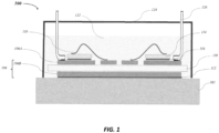
- FIG. 1 is a representative cross-sectional view of a power semiconductor device 100 (hereinafter "the device 100") according to exemplary embodiments of the present disclosure.
- the device 100 may include a metal heatsink 102, which pulls heat away from other components of the device and forms the baseplate of the device 100.
- a multilayer substrate 104 may be positioned atop the heatsink 102 and may include first and second conductive layers 106A and 106B (collectively, "the conductive layers 106") disposed on top and bottom surfaces of an insulating layer 110.
- the conductive layers 106 may be formed of copper and the insulating layer 110 may be formed of ceramic (e.g., aluminum oxide, aluminum nitride, etc.). The present disclosure is not limited in this regard.
- the substrate 104 may be soldered or sintered to the heatsink 102 by a solder or sinter layer 112.
- Silicon or silicon-based semiconductor chips or dies 114 may be connected to a top surface of the first conductive layer 106A of the substrate 104 by a solder or sinter layer 116.
- Metal wires, ribbons, clips, or the like (hereinafter “the metal wires 118") may connect top surfaces of the semiconductor dies 114 to portions of first conductive layer 106A, thus providing electrical interconnections within the package.
- Contact elements/terminal leads 120 (hereinafter referred to as "the terminals 120") may also be connected to the top surface of the first conductive layer 106A of the substrate 104 as further described below.
- the terminals 120 may be formed of highly electrically conductive metals, such as copper, copper alloy, aluminum, aluminum alloy, silver, or silver alloy. Additionally, the terminals 120 may be plated with nickel, silver, or gold, which may be physically or chemically applied to the surfaces of the terminals 120. The present disclosure is not limited in this regard.
- An encapsulation layer 122 may encase the circuit components above the heatsink 102, and a cover 124 formed of a durable, dielectric material (e.g., plastic) may be disposed over the circuit components and may protect the circuit components from external elements, with portions of the terminals 120 protruding from the cover 124 for facilitating electrical connection of the device 100 within a circuit.
- the encapsulation layer 122 may be formed of silicone gel, epoxy molding compound (EMC), or mixtures thereof.
- EMC epoxy molding compound
- embodiments of the device 100 are contemplated in which the cover 124 is entirely omitted, such as if the device 100 includes module-type semiconductor packing with EMC used for the encapsulation layer 122. The present disclosure is not limited in this regard.
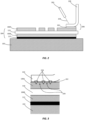
- FIG. 2 there is shown a cross-sectional view of the above-described device 100 during an assembly step thereof, wherein one of the terminals 120 is being bonded to the first conductive layer 106A of the substrate 104 using a laser bonding technique in accordance with embodiments of the present disclosure.
- a thin metallic layer 202 may be disposed atop the first conductive layer 106A, and the terminal 120 may then be placed atop the thin metallic layer 202.
- the thin metallic layer 202 may be formed of tin or other metals and/or metal alloys having good electrical conductivity and a low melting point (e.g., a melting point below 450 degrees Celsius).
- the thin metallic layer 202 may have a melting point lower than that of the material from which the terminal 120 is formed.
- the thin metallic layer 202 may be a thin sheet of metal or foil.
- the thin metallic layer 202 may be formed of solder paste, sinter paste, etc.
- the thin metallic layer 202 may have a thickness in a range of 20-100 ⁇ m. The present disclosure is not limited in this regard.
- the laser bonding technique of the present disclosure employs laser treatment to affix or bond the terminal 120 to the first conductive layer 106A in a manner sufficient to allow electrical current to flow from the terminal 120 to the first conductive layer 106A and vice-versa.
- a laser beam 204 may be directed at a top surface of the terminal 120 above an area where the terminal 120 is to be bonded to the first conductive layer 106A, hereinafter referred to as "the bonding region 206."
- the energy of the laser beam 204 causes the solid materials of the terminal 120 and the first conductive layer 106A to be transformed (melted with consecutive rapid solidification), resulting in weld connections 208 therebetween as shown in the detailed view of FIG. 3 .
- the weld connections 208 may be separated by spaces or gaps 209 (as dictated by the particular weld pattern employed) where the terminal 120 and the first conductive layer 106A are not welded together. However, heat generated by the laser treatment may be sufficient to melt the thin metallic layer 202, whereafter the molten material of the thin metallic layer 202 may flow into the gaps 209 as motivated by capillary forces and wettability of the surrounding surfaces of the terminal 120 and the first conductive layer 106A. After filing the gaps 209 between/adjacent the weld connections 208, the molten material of the thin metallic layer 202 may cool and solidify and, in combination with the weld connections 208, may provide robust electrical and mechanical connections between the terminal 120 and the first conductive layer 106A.
- the laser bonding technique of the present disclosure thereby reduces the likelihood of mechanical failure (e.g., cracking) in the bonding region 206 and improves the conductivity and reliability of the bond relative to traditional laser bonding techniques.
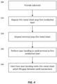
- FIG. 4 a flow diagram illustrating an embodiment of the laser bonding technique of the present disclosure is shown. The method will now be described in conjunction with the illustrations of the device 100 shown in FIGS. 2 and 3 .
- the substrate 104 may be provided, wherein the substrate 104 includes the insulating layer 110 and first and second conductive layers 106A,106B disposed on top and bottom surfaces of the insulating layer 110, respectively.
- the substrate 104 may be positioned atop a heatsink 102 with the second conductive layer 106B soldered or sintered to the heatsink 102.
- the thin metallic layer 202 formed of a low melting point metal may be disposed atop the first conductive layer 106A.
- the terminal 120 may be placed atop the thin metallic layer 202.
- the laser device 203 may be used to direct the laser beam 204 at the top surface of the terminal 120 above an area where the terminal 120 is to be bonded to the first conductive layer 106A.
- the energy of the laser beam 204 may melt the solid materials of the terminal 120 and the first conductive layer 106A to be transformed (melted with consecutive rapid solidification), resulting in weld connections 208 therebetween.
- heat generated by the laser treatment may melt the thin metallic layer 202, whereafter the molten material of the thin metallic layer 202 may flow into the gaps 209 as motivated by capillary forces and wettability of the surrounding surfaces of the terminal 120 and the first conductive layer 106A.
- the molten material of the thin metallic layer 202 may cool and solidify and, in combination with the weld connections 208, may provide robust electrical and mechanical connections between the terminal 120 and the first conductive layer 106A.
Landscapes
- Engineering & Computer Science (AREA)
- Microelectronics & Electronic Packaging (AREA)
- Laser Beam Processing (AREA)
- Cooling Or The Like Of Semiconductors Or Solid State Devices (AREA)
- Chemical & Material Sciences (AREA)
- Ceramic Engineering (AREA)
Abstract
Description
- Embodiments of the present disclosure relate to power semiconductors and, more particularly, to a technique for connecting a power terminal to a substrate within a power module semiconductor package.
- Power semiconductors are components used to convert energy from one form to another at various stages between the points of energy generation and energy consumption. A power semiconductor component can take the form of a discrete transistor, thyristor, diode, insulated gate bipolar transistor (IGBT), or metal oxide semiconductor field effect transistor (MOSFET). Or, if a higher level of current or integration is required, the component can take the form of a multi-chip module, which contains more than one of these chips or dies in a desired configuration or topology. Power semiconductors may be packaged in a variety of discrete and multi-chip module formats.
- Power semiconductor devices include power terminals extending from the semiconductor packaging for connection to printed circuit boards and other circuit elements. The power terminals may be connected to the semiconductor packaging using conventional technologies such as soldering, sintering, and welding, e.g., high-current pulse welding, and ultrasonic welding. However, ultrasonic welding is messy, as particles, whiskers, or debris-like particles are generated during the welding process. Further, the generated debris is electrically conductive and able to disturb the function of the power semiconductor unit and/or the substrate of the semiconductor packaging may be cracked or otherwise damaged during the ultrasonic welding process.
- To address the shortcomings described above,
United States Patent No. 10,720,376 - It is with respect to these and other considerations that the present improvements may be useful.
- This Summary is provided to introduce a selection of concepts in a simplified form that are further described below in the Detailed Description. This Summary is not intended to identify key or essential features of the claimed subject matter, nor is it intended as an aid in determining the scope of the claimed subject matter.
- A power seimcodnuctor device in accordance with an embodiment of the present disclosure may include a heatsink, a substrate disposed atop the heatsink, a semiconductor die disposed atop, and electrically connected to, the substrate, and a terminal disposed atop, and electrically connected to, the substrate by weld connections separated by gaps, wherein the gaps are filled by a thin metallic layer.
- A method of manufacturing a power semiconductor device in accordance with an embodiment of the present disclosure may include providing a substrate disposed atop a heatsink, electrically connecting a semiconductor die to a top surface of the substrate, disposing a thin metallic layer atop the substrate, disposing a terminal atop the thin metallic layer, and performing a welding operation wherein a laser beam is directed at a top surface of the terminal to produce a plurality of weld connections connecting the terminal to the substrate, wherein the weld connections are separated by gaps, and wherein heat generated during the welding operation melts the thin metallic layer and molten material of the thin metallic flows into the gaps.
-
-
FIG. 1 is a cross-sectional view illustrating a power semiconductor device in accordance with an exemplary embodiment of the present disclosure; -
FIG. 2 is a cross-sectional view illustrating the power semiconductor device ofFIG. 1 during an assembly step thereof in accordance with an exemplary embodiment of the present disclosure; -
FIG. 3 is a detailed cross-sectional view illustrating a bonding region between a terminal lead and a substrate of the power semiconductor device ofFIG. 1 ; -
FIG. 4 is a flow diagram illustrating an exemplary laser bonding method for connecting a terminal lead to a substrate of the power semiconductor device ofFIG. 1 . - Embodiments of a laser bonding method and an associated power semiconductor device in accordance with the present disclosure will now be described more fully with reference to the accompanying drawings, in which preferred embodiments of the present disclosure are presented. The method and device of the present disclosure may, however, be embodied in many different forms and should not be construed as being limited to the embodiments set forth herein. Rather, these embodiments are provided so that this disclosure will be thorough and complete, and will fully convey the scope of the method and device to those skilled in the art. In the drawings, like numbers refer to like elements throughout unless otherwise noted.
-
FIG. 1 is a representative cross-sectional view of a power semiconductor device 100 (hereinafter "thedevice 100") according to exemplary embodiments of the present disclosure. Thedevice 100 may include ametal heatsink 102, which pulls heat away from other components of the device and forms the baseplate of thedevice 100. Amultilayer substrate 104 may be positioned atop theheatsink 102 and may include first and secondconductive layers insulating layer 110. In various embodiments, the conductive layers 106 may be formed of copper and theinsulating layer 110 may be formed of ceramic (e.g., aluminum oxide, aluminum nitride, etc.). The present disclosure is not limited in this regard. - The
substrate 104 may be soldered or sintered to theheatsink 102 by a solder orsinter layer 112. Silicon or silicon-based semiconductor chips or dies 114 may be connected to a top surface of the firstconductive layer 106A of thesubstrate 104 by a solder orsinter layer 116. Metal wires, ribbons, clips, or the like (hereinafter "themetal wires 118") may connect top surfaces of the semiconductor dies 114 to portions of firstconductive layer 106A, thus providing electrical interconnections within the package. Contact elements/terminal leads 120 (hereinafter referred to as "theterminals 120") may also be connected to the top surface of the firstconductive layer 106A of thesubstrate 104 as further described below. In exemplary embodiments, theterminals 120 may be formed of highly electrically conductive metals, such as copper, copper alloy, aluminum, aluminum alloy, silver, or silver alloy. Additionally, theterminals 120 may be plated with nickel, silver, or gold, which may be physically or chemically applied to the surfaces of theterminals 120. The present disclosure is not limited in this regard. - An
encapsulation layer 122 may encase the circuit components above theheatsink 102, and acover 124 formed of a durable, dielectric material (e.g., plastic) may be disposed over the circuit components and may protect the circuit components from external elements, with portions of theterminals 120 protruding from thecover 124 for facilitating electrical connection of thedevice 100 within a circuit. In various embodiments, theencapsulation layer 122 may be formed of silicone gel, epoxy molding compound (EMC), or mixtures thereof. Additionally, embodiments of thedevice 100 are contemplated in which thecover 124 is entirely omitted, such as if thedevice 100 includes module-type semiconductor packing with EMC used for theencapsulation layer 122. The present disclosure is not limited in this regard. - Referring to
FIG. 2 , there is shown a cross-sectional view of the above-describeddevice 100 during an assembly step thereof, wherein one of theterminals 120 is being bonded to the firstconductive layer 106A of thesubstrate 104 using a laser bonding technique in accordance with embodiments of the present disclosure. During this assembly step, a thinmetallic layer 202 may be disposed atop the firstconductive layer 106A, and theterminal 120 may then be placed atop the thinmetallic layer 202. The thinmetallic layer 202 may be formed of tin or other metals and/or metal alloys having good electrical conductivity and a low melting point (e.g., a melting point below 450 degrees Celsius). More generally, the thinmetallic layer 202 may have a melting point lower than that of the material from which theterminal 120 is formed. In various embodiments, the thinmetallic layer 202 may be a thin sheet of metal or foil. In other embodiments, the thinmetallic layer 202 may be formed of solder paste, sinter paste, etc. The thinmetallic layer 202 may have a thickness in a range of 20-100µm. The present disclosure is not limited in this regard. - Using a
laser device 203, the laser bonding technique of the present disclosure employs laser treatment to affix or bond theterminal 120 to the firstconductive layer 106A in a manner sufficient to allow electrical current to flow from theterminal 120 to the firstconductive layer 106A and vice-versa. Particularly, alaser beam 204 may be directed at a top surface of theterminal 120 above an area where theterminal 120 is to be bonded to the firstconductive layer 106A, hereinafter referred to as "thebonding region 206." The energy of thelaser beam 204 causes the solid materials of theterminal 120 and the firstconductive layer 106A to be transformed (melted with consecutive rapid solidification), resulting inweld connections 208 therebetween as shown in the detailed view ofFIG. 3 . - The
weld connections 208 may be separated by spaces or gaps 209 (as dictated by the particular weld pattern employed) where theterminal 120 and the firstconductive layer 106A are not welded together. However, heat generated by the laser treatment may be sufficient to melt the thinmetallic layer 202, whereafter the molten material of the thinmetallic layer 202 may flow into thegaps 209 as motivated by capillary forces and wettability of the surrounding surfaces of theterminal 120 and the firstconductive layer 106A. After filing thegaps 209 between/adjacent theweld connections 208, the molten material of the thinmetallic layer 202 may cool and solidify and, in combination with theweld connections 208, may provide robust electrical and mechanical connections between theterminal 120 and the firstconductive layer 106A. The laser bonding technique of the present disclosure thereby reduces the likelihood of mechanical failure (e.g., cracking) in thebonding region 206 and improves the conductivity and reliability of the bond relative to traditional laser bonding techniques. - Referring to
FIG. 4 , a flow diagram illustrating an embodiment of the laser bonding technique of the present disclosure is shown. The method will now be described in conjunction with the illustrations of thedevice 100 shown inFIGS. 2 and 3 . - At
block 300 of the exemplary method, thesubstrate 104 may be provided, wherein thesubstrate 104 includes theinsulating layer 110 and first and secondconductive layers insulating layer 110, respectively. Thesubstrate 104 may be positioned atop aheatsink 102 with the secondconductive layer 106B soldered or sintered to theheatsink 102. Atblock 310 of the method, the thinmetallic layer 202 formed of a low melting point metal may be disposed atop the firstconductive layer 106A. Atblock 320 of the method, the terminal 120 may be placed atop the thinmetallic layer 202. - At
block 330 of the exemplary method, thelaser device 203 may be used to direct thelaser beam 204 at the top surface of the terminal 120 above an area where the terminal 120 is to be bonded to the firstconductive layer 106A. The energy of thelaser beam 204 may melt the solid materials of the terminal 120 and the firstconductive layer 106A to be transformed (melted with consecutive rapid solidification), resulting inweld connections 208 therebetween. Atblock 340 of the method, which may happen simultaneously with the action ofblock 330, heat generated by the laser treatment may melt the thinmetallic layer 202, whereafter the molten material of the thinmetallic layer 202 may flow into thegaps 209 as motivated by capillary forces and wettability of the surrounding surfaces of the terminal 120 and the firstconductive layer 106A. After filling thegaps 209 between/adjacent theweld connections 208, the molten material of the thinmetallic layer 202 may cool and solidify and, in combination with theweld connections 208, may provide robust electrical and mechanical connections between the terminal 120 and the firstconductive layer 106A. - As used herein, an element or step recited in the singular and proceeded with the word "a" or "an" should be understood as not excluding plural elements or steps, unless such exclusion is explicitly recited. Furthermore, references to "one embodiment" of the present disclosure are not intended to be interpreted as excluding the existence of additional embodiments that also incorporate the recited features.
- While the present disclosure makes reference to certain embodiments, numerous modifications, alterations and changes to the described embodiments are possible without departing from the sphere and scope of the present disclosure, as defined in the appended claim(s). Accordingly, it is intended that the present disclosure not be limited to the described embodiments, but that it has the full scope defined by the language of the following claims, and equivalents thereof.
Claims (15)
- A power semiconductor device comprising:a heatsink;a substrate disposed atop the heatsink;a semiconductor die disposed atop, and electrically connected to, the substrate; anda terminal disposed atop, and electrically connected to, the substrate by weld connections separated by gaps, wherein the gaps are filled by a thin metallic layer.
- The power semiconductor device of claim 1, wherein the thin metallic layer is formed of a metal different from a metal from which the weld connections are formed.
- The power semiconductor device of claim 1 or 2, wherein the substrate is a multilayer structure that includes an insulating layer, a first conductive layer disposed on a top surface of the insulating layer, and a second conductive layer disposed on a bottom surface of the insulating layer,preferably wherein the first and second conductive layers are formed of copper, and/orwherein the insulating layer is formed of ceramic.
- The power semiconductor device of any of the preceding claims, wherein the terminal is formed of one of copper, copper alloy, aluminum, aluminum alloy, silver, and silver alloy.
- The power semiconductor device of any of the preceding claims, wherein the terminal is plated with one of nickel, silver, and gold.
- The power semiconductor device of any of the preceding claims, further comprising an encapsulation layer that covers and encases the semiconductor die and the terminal with a portion of the terminal protruding from the encapsulation layer, preferably wherein the encapsulation layer is formed of at least one of silicone gel and epoxy molding compound.
- The power semiconductor device of any of the preceding claims, wherein the thin metallic layer has a thickness in a range of 20-100µm.
- A method of manufacturing a power semiconductor device, the method comprising:providing a substrate disposed atop a heatsink;electrically connecting a semiconductor die to a top surface of the substrate;disposing a thin metallic layer atop the substrate;disposing a terminal atop the thin metallic layer; andperforming a welding operation wherein a laser beam is directed at a top surface of the terminal to produce a plurality of weld connections connecting the terminal to the substrate, wherein the weld connections are separated by gaps, and wherein heat generated during the welding operation melts the thin metallic layer, and molten material of the thin metallic layer flows into the gaps.
- The method of claim 8, wherein the thin metallic layer is formed of a metal different from a metal from which the weld connections are formed.
- The method of claim 8 or 9, wherein the substrate is a multilayer structure that includes an insulating layer, a first conductive layer disposed on a top surface of the insulating layer, and a second conductive layer disposed on a bottom surface of the insulating layer,preferably wherein the first and second conductive layers are formed of copper, and/orwherein the insulating layer is formed of ceramic.
- The method of any of the claims 8-10, wherein the terminal is formed of one of copper, copper alloy, aluminum, aluminum alloy, silver, and silver alloy.
- The method of any of the claims 8-11, wherein the terminal is plated with one of nickel, silver, and gold.
- The method of any of the claims 8-12,- further comprising an encapsulation layer that covers and encases the semiconductor die and the terminal with a portion of the terminal protruding from the encapsulation layer.
- The method of claim 13, wherein the encapsulation layer is formed of at least one of silicone gel and epoxy molding compound.
- The method of any of the claims 8-14. wherein the thin metallic layer has a thickness in a range of 20-100µm.
Applications Claiming Priority (1)
| Application Number | Priority Date | Filing Date | Title |
|---|---|---|---|
| US18/136,554 US12543611B2 (en) | 2023-04-19 | 2023-04-19 | Method to connect power terminal to substrate within semiconductor package |
Publications (1)
| Publication Number | Publication Date |
|---|---|
| EP4451315A1 true EP4451315A1 (en) | 2024-10-23 |
Family
ID=90720204
Family Applications (1)
| Application Number | Title | Priority Date | Filing Date |
|---|---|---|---|
| EP24169302.7A Pending EP4451315A1 (en) | 2023-04-19 | 2024-04-09 | Method to connect power terminal to substrate within semiconductor package |
Country Status (5)
| Country | Link |
|---|---|
| US (1) | US12543611B2 (en) |
| EP (1) | EP4451315A1 (en) |
| KR (1) | KR102906822B1 (en) |
| CN (1) | CN118824985A (en) |
| TW (1) | TWI890401B (en) |
Citations (4)
| Publication number | Priority date | Publication date | Assignee | Title |
|---|---|---|---|---|
| US10720376B2 (en) | 2012-01-05 | 2020-07-21 | Littelfuse, Inc. | Discrete power transistor package having solderless DBC to leadframe attach |
| US20210407954A1 (en) * | 2018-11-22 | 2021-12-30 | Rohm Co., Ltd. | Semiconductor device |
| JP2022026626A (en) * | 2020-07-31 | 2022-02-10 | 三菱電機株式会社 | Semiconductor device and manufacturing method therefor |
| US20220310409A1 (en) * | 2021-03-24 | 2022-09-29 | Littelfuse, Inc. | Method to connect power terminal to substrate within semiconductor package |
Family Cites Families (7)
| Publication number | Priority date | Publication date | Assignee | Title |
|---|---|---|---|---|
| WO2002027786A1 (en) * | 2000-09-25 | 2002-04-04 | Ibiden Co., Ltd. | Semiconductor element, method of manufacturing semiconductor element, multi-layer printed circuit board, and method of manufacturing multi-layer printed circuit board |
| JP2009105266A (en) | 2007-10-24 | 2009-05-14 | Fuji Electric Device Technology Co Ltd | Method of manufacturing semiconductor apparatus |
| JP2009252799A (en) * | 2008-04-01 | 2009-10-29 | Nitto Denko Corp | Method for manufacturing semiconductor device |
| JP6356550B2 (en) * | 2014-09-10 | 2018-07-11 | 三菱電機株式会社 | Semiconductor device and manufacturing method thereof |
| KR20170130179A (en) | 2016-05-18 | 2017-11-28 | 엘지전자 주식회사 | Insulating substrate using thick film printing |
| DE112020001100T5 (en) | 2019-03-05 | 2022-01-05 | Rohm Co., Ltd. | SEMICONDUCTOR COMPONENT AND BOND PROCESS |
| US20230075909A1 (en) | 2021-09-09 | 2023-03-09 | Taiwan Semiconductor Manufacturing Company, Ltd. | Electronic apparatus, semiconductor package module and manufacturing method thereof |
-
2023
- 2023-04-19 US US18/136,554 patent/US12543611B2/en active Active
-
2024
- 2024-04-09 EP EP24169302.7A patent/EP4451315A1/en active Pending
- 2024-04-09 TW TW113113053A patent/TWI890401B/en active
- 2024-04-17 KR KR1020240051545A patent/KR102906822B1/en active Active
- 2024-04-19 CN CN202410474733.2A patent/CN118824985A/en active Pending
Patent Citations (4)
| Publication number | Priority date | Publication date | Assignee | Title |
|---|---|---|---|---|
| US10720376B2 (en) | 2012-01-05 | 2020-07-21 | Littelfuse, Inc. | Discrete power transistor package having solderless DBC to leadframe attach |
| US20210407954A1 (en) * | 2018-11-22 | 2021-12-30 | Rohm Co., Ltd. | Semiconductor device |
| JP2022026626A (en) * | 2020-07-31 | 2022-02-10 | 三菱電機株式会社 | Semiconductor device and manufacturing method therefor |
| US20220310409A1 (en) * | 2021-03-24 | 2022-09-29 | Littelfuse, Inc. | Method to connect power terminal to substrate within semiconductor package |
Also Published As
| Publication number | Publication date |
|---|---|
| CN118824985A (en) | 2024-10-22 |
| TWI890401B (en) | 2025-07-11 |
| US20240355718A1 (en) | 2024-10-24 |
| KR102906822B1 (en) | 2026-01-06 |
| KR20240155794A (en) | 2024-10-29 |
| TW202443828A (en) | 2024-11-01 |
| US12543611B2 (en) | 2026-02-03 |
Similar Documents
| Publication | Publication Date | Title |
|---|---|---|
| US10510640B2 (en) | Semiconductor device and method for manufacturing semiconductor device | |
| CN102244016B (en) | Resin sealing type semiconductor device and method of manufacturing the same, and lead frame | |
| CN103035601B (en) | Include the semiconductor devices of Diffusion Welding layer on sintering silver layer | |
| US8298867B2 (en) | Method for fabricating a circuit substrate assembly and a power electronics module comprising an anchoring structure for producing a changing temperature-stable solder bond | |
| US20060056213A1 (en) | Power module package having excellent heat sink emission capability and method for manufacturing the same | |
| US11276629B2 (en) | Semiconductor device | |
| JPH08510358A (en) | Interconnection of integrated circuit chips and substrates | |
| TW200522328A (en) | Semiconductor device and manufacturing method thereof | |
| KR102228945B1 (en) | Semiconductor package and method of fabricating the same | |
| EP4064329A2 (en) | Method to connect power terminal to substrate within semiconductor package | |
| US10872846B2 (en) | Solid top terminal for discrete power devices | |
| JP5233853B2 (en) | Semiconductor device | |
| CN111433910B (en) | Semiconductor device and method of manufacturing semiconductor device | |
| CN104835796A (en) | Lead-free diffusion welding power module | |
| US10236244B2 (en) | Semiconductor device and production method therefor | |
| US12543611B2 (en) | Method to connect power terminal to substrate within semiconductor package | |
| JP7334655B2 (en) | semiconductor equipment | |
| CN114078716A (en) | Semiconductor device and method for manufacturing the same | |
| CN100435328C (en) | molded package | |
| JP7582156B2 (en) | Semiconductor device and its manufacturing method | |
| JP7390826B2 (en) | Semiconductor device and semiconductor device manufacturing method | |
| CN118476020A (en) | Resin-sealed semiconductor device | |
| JP4861200B2 (en) | Power module | |
| JP2006041363A (en) | Resin-sealed semiconductor device | |
| KR102684854B1 (en) | Semiconductor package and method of fabricating the same |
Legal Events
| Date | Code | Title | Description |
|---|---|---|---|
| PUAI | Public reference made under article 153(3) epc to a published international application that has entered the european phase |
Free format text: ORIGINAL CODE: 0009012 |
|
| STAA | Information on the status of an ep patent application or granted ep patent |
Free format text: STATUS: THE APPLICATION HAS BEEN PUBLISHED |
|
| AK | Designated contracting states |
Kind code of ref document: A1 Designated state(s): AL AT BE BG CH CY CZ DE DK EE ES FI FR GB GR HR HU IE IS IT LI LT LU LV MC ME MK MT NL NO PL PT RO RS SE SI SK SM TR |
|
| STAA | Information on the status of an ep patent application or granted ep patent |
Free format text: STATUS: REQUEST FOR EXAMINATION WAS MADE |
|
| 17P | Request for examination filed |
Effective date: 20250414 |
|
| RIC1 | Information provided on ipc code assigned before grant |
Ipc: H01L 21/48 20060101AFI20250723BHEP Ipc: H01L 23/373 20060101ALI20250723BHEP Ipc: H01L 23/498 20060101ALI20250723BHEP Ipc: H01L 25/07 20060101ALI20250723BHEP Ipc: H01L 23/053 20060101ALI20250723BHEP Ipc: H01L 23/36 20060101ALN20250723BHEP Ipc: H01L 25/00 20060101ALN20250723BHEP Ipc: H01L 23/00 20060101ALN20250723BHEP Ipc: H01L 23/24 20060101ALN20250723BHEP |
|
| RIC1 | Information provided on ipc code assigned before grant |
Ipc: H01L 21/48 20060101AFI20250912BHEP Ipc: H01L 23/373 20060101ALI20250912BHEP Ipc: H01L 23/498 20060101ALI20250912BHEP Ipc: H01L 25/07 20060101ALI20250912BHEP Ipc: H01L 23/053 20060101ALI20250912BHEP Ipc: H01L 23/36 20060101ALN20250912BHEP Ipc: H01L 25/00 20060101ALN20250912BHEP Ipc: H01L 23/00 20060101ALN20250912BHEP Ipc: H01L 23/24 20060101ALN20250912BHEP |
|
| GRAP | Despatch of communication of intention to grant a patent |
Free format text: ORIGINAL CODE: EPIDOSNIGR1 |
|
| STAA | Information on the status of an ep patent application or granted ep patent |
Free format text: STATUS: GRANT OF PATENT IS INTENDED |
|
| RIC1 | Information provided on ipc code assigned before grant |
Ipc: H01L 21/48 20060101AFI20251015BHEP Ipc: H01L 23/373 20060101ALI20251015BHEP Ipc: H01L 23/498 20060101ALI20251015BHEP Ipc: H01L 25/07 20060101ALI20251015BHEP Ipc: H01L 23/053 20060101ALI20251015BHEP Ipc: H01L 23/36 20060101ALN20251015BHEP Ipc: H01L 25/00 20060101ALN20251015BHEP Ipc: H01L 23/00 20060101ALN20251015BHEP Ipc: H01L 23/24 20060101ALN20251015BHEP |
|
| RIC1 | Information provided on ipc code assigned before grant |
Ipc: H01L 21/48 20060101AFI20251022BHEP Ipc: H01L 23/373 20060101ALI20251022BHEP Ipc: H01L 23/498 20060101ALI20251022BHEP Ipc: H01L 25/07 20060101ALI20251022BHEP Ipc: H01L 23/053 20060101ALI20251022BHEP Ipc: H01L 23/36 20060101ALN20251022BHEP Ipc: H01L 25/00 20060101ALN20251022BHEP Ipc: H01L 23/00 20060101ALN20251022BHEP Ipc: H01L 23/24 20060101ALN20251022BHEP |
|
| INTG | Intention to grant announced |
Effective date: 20251118 |
|
| GRAJ | Information related to disapproval of communication of intention to grant by the applicant or resumption of examination proceedings by the epo deleted |
Free format text: ORIGINAL CODE: EPIDOSDIGR1 |
|
| STAA | Information on the status of an ep patent application or granted ep patent |
Free format text: STATUS: REQUEST FOR EXAMINATION WAS MADE |
|
| REG | Reference to a national code |
Ref country code: DE Ref legal event code: R079 Free format text: PREVIOUS MAIN CLASS: H01L0021480000 Ipc: H10W0099000000 |
|
| INTC | Intention to grant announced (deleted) | ||
| RIC1 | Information provided on ipc code assigned before grant |
Ipc: H10W 99/00 20260101AFI20260112BHEP Ipc: H10W 40/25 20260101ALI20260112BHEP Ipc: H10W 70/60 20260101ALI20260112BHEP Ipc: H10W 90/00 20260101ALI20260112BHEP Ipc: H10W 76/15 20260101ALI20260112BHEP Ipc: H10W 40/10 20260101ALN20260112BHEP Ipc: H10W 76/47 20260101ALN20260112BHEP |
|
| GRAP | Despatch of communication of intention to grant a patent |
Free format text: ORIGINAL CODE: EPIDOSNIGR1 |
|
| STAA | Information on the status of an ep patent application or granted ep patent |
Free format text: STATUS: GRANT OF PATENT IS INTENDED |
|
| INTG | Intention to grant announced |
Effective date: 20260302 |
|
| P01 | Opt-out of the competence of the unified patent court (upc) registered |
Free format text: CASE NUMBER: UPC_APP_0009317_4451315/2026 Effective date: 20260311 |