EP4451256A1 - Light-emitting drive circuit, timing control method, and display panel - Google Patents
Light-emitting drive circuit, timing control method, and display panel Download PDFInfo
- Publication number
- EP4451256A1 EP4451256A1 EP23904832.5A EP23904832A EP4451256A1 EP 4451256 A1 EP4451256 A1 EP 4451256A1 EP 23904832 A EP23904832 A EP 23904832A EP 4451256 A1 EP4451256 A1 EP 4451256A1
- Authority
- EP
- European Patent Office
- Prior art keywords
- pull
- potential
- light
- transistor
- node
- Prior art date
- Legal status (The legal status is an assumption and is not a legal conclusion. Google has not performed a legal analysis and makes no representation as to the accuracy of the status listed.)
- Pending
Links
Images
Classifications
-
- G—PHYSICS
- G09—EDUCATION; CRYPTOGRAPHY; DISPLAY; ADVERTISING; SEALS
- G09G—ARRANGEMENTS OR CIRCUITS FOR CONTROL OF INDICATING DEVICES USING STATIC MEANS TO PRESENT VARIABLE INFORMATION
- G09G3/00—Control arrangements or circuits, of interest only in connection with visual indicators other than cathode-ray tubes
- G09G3/20—Control arrangements or circuits, of interest only in connection with visual indicators other than cathode-ray tubes for presentation of an assembly of a number of characters, e.g. a page, by composing the assembly by combination of individual elements arranged in a matrix no fixed position being assigned to or needed to be assigned to the individual characters or partial characters
- G09G3/22—Control arrangements or circuits, of interest only in connection with visual indicators other than cathode-ray tubes for presentation of an assembly of a number of characters, e.g. a page, by composing the assembly by combination of individual elements arranged in a matrix no fixed position being assigned to or needed to be assigned to the individual characters or partial characters using controlled light sources
- G09G3/30—Control arrangements or circuits, of interest only in connection with visual indicators other than cathode-ray tubes for presentation of an assembly of a number of characters, e.g. a page, by composing the assembly by combination of individual elements arranged in a matrix no fixed position being assigned to or needed to be assigned to the individual characters or partial characters using controlled light sources using electroluminescent panels
- G09G3/32—Control arrangements or circuits, of interest only in connection with visual indicators other than cathode-ray tubes for presentation of an assembly of a number of characters, e.g. a page, by composing the assembly by combination of individual elements arranged in a matrix no fixed position being assigned to or needed to be assigned to the individual characters or partial characters using controlled light sources using electroluminescent panels semiconductive, e.g. using light-emitting diodes [LED]
- G09G3/3208—Control arrangements or circuits, of interest only in connection with visual indicators other than cathode-ray tubes for presentation of an assembly of a number of characters, e.g. a page, by composing the assembly by combination of individual elements arranged in a matrix no fixed position being assigned to or needed to be assigned to the individual characters or partial characters using controlled light sources using electroluminescent panels semiconductive, e.g. using light-emitting diodes [LED] organic, e.g. using organic light-emitting diodes [OLED]
- G09G3/3266—Details of drivers for scan electrodes
-
- G—PHYSICS
- G09—EDUCATION; CRYPTOGRAPHY; DISPLAY; ADVERTISING; SEALS
- G09G—ARRANGEMENTS OR CIRCUITS FOR CONTROL OF INDICATING DEVICES USING STATIC MEANS TO PRESENT VARIABLE INFORMATION
- G09G3/00—Control arrangements or circuits, of interest only in connection with visual indicators other than cathode-ray tubes
- G09G3/20—Control arrangements or circuits, of interest only in connection with visual indicators other than cathode-ray tubes for presentation of an assembly of a number of characters, e.g. a page, by composing the assembly by combination of individual elements arranged in a matrix no fixed position being assigned to or needed to be assigned to the individual characters or partial characters
- G09G3/22—Control arrangements or circuits, of interest only in connection with visual indicators other than cathode-ray tubes for presentation of an assembly of a number of characters, e.g. a page, by composing the assembly by combination of individual elements arranged in a matrix no fixed position being assigned to or needed to be assigned to the individual characters or partial characters using controlled light sources
- G09G3/30—Control arrangements or circuits, of interest only in connection with visual indicators other than cathode-ray tubes for presentation of an assembly of a number of characters, e.g. a page, by composing the assembly by combination of individual elements arranged in a matrix no fixed position being assigned to or needed to be assigned to the individual characters or partial characters using controlled light sources using electroluminescent panels
- G09G3/32—Control arrangements or circuits, of interest only in connection with visual indicators other than cathode-ray tubes for presentation of an assembly of a number of characters, e.g. a page, by composing the assembly by combination of individual elements arranged in a matrix no fixed position being assigned to or needed to be assigned to the individual characters or partial characters using controlled light sources using electroluminescent panels semiconductive, e.g. using light-emitting diodes [LED]
- G09G3/3208—Control arrangements or circuits, of interest only in connection with visual indicators other than cathode-ray tubes for presentation of an assembly of a number of characters, e.g. a page, by composing the assembly by combination of individual elements arranged in a matrix no fixed position being assigned to or needed to be assigned to the individual characters or partial characters using controlled light sources using electroluminescent panels semiconductive, e.g. using light-emitting diodes [LED] organic, e.g. using organic light-emitting diodes [OLED]
- G09G3/3225—Control arrangements or circuits, of interest only in connection with visual indicators other than cathode-ray tubes for presentation of an assembly of a number of characters, e.g. a page, by composing the assembly by combination of individual elements arranged in a matrix no fixed position being assigned to or needed to be assigned to the individual characters or partial characters using controlled light sources using electroluminescent panels semiconductive, e.g. using light-emitting diodes [LED] organic, e.g. using organic light-emitting diodes [OLED] using an active matrix
-
- G—PHYSICS
- G09—EDUCATION; CRYPTOGRAPHY; DISPLAY; ADVERTISING; SEALS
- G09G—ARRANGEMENTS OR CIRCUITS FOR CONTROL OF INDICATING DEVICES USING STATIC MEANS TO PRESENT VARIABLE INFORMATION
- G09G2300/00—Aspects of the constitution of display devices
- G09G2300/04—Structural and physical details of display devices
- G09G2300/0421—Structural details of the set of electrodes
- G09G2300/0426—Layout of electrodes and connections
-
- G—PHYSICS
- G09—EDUCATION; CRYPTOGRAPHY; DISPLAY; ADVERTISING; SEALS
- G09G—ARRANGEMENTS OR CIRCUITS FOR CONTROL OF INDICATING DEVICES USING STATIC MEANS TO PRESENT VARIABLE INFORMATION
- G09G2300/00—Aspects of the constitution of display devices
- G09G2300/08—Active matrix structure, i.e. with use of active elements, inclusive of non-linear two terminal elements, in the pixels together with light emitting or modulating elements
- G09G2300/0809—Several active elements per pixel in active matrix panels
- G09G2300/0842—Several active elements per pixel in active matrix panels forming a memory circuit, e.g. a dynamic memory with one capacitor
- G09G2300/0861—Several active elements per pixel in active matrix panels forming a memory circuit, e.g. a dynamic memory with one capacitor with additional control of the display period without amending the charge stored in a pixel memory, e.g. by means of additional select electrodes
-
- G—PHYSICS
- G09—EDUCATION; CRYPTOGRAPHY; DISPLAY; ADVERTISING; SEALS
- G09G—ARRANGEMENTS OR CIRCUITS FOR CONTROL OF INDICATING DEVICES USING STATIC MEANS TO PRESENT VARIABLE INFORMATION
- G09G2310/00—Command of the display device
- G09G2310/02—Addressing, scanning or driving the display screen or processing steps related thereto
- G09G2310/0264—Details of driving circuits
- G09G2310/0286—Details of a shift registers arranged for use in a driving circuit
-
- G—PHYSICS
- G09—EDUCATION; CRYPTOGRAPHY; DISPLAY; ADVERTISING; SEALS
- G09G—ARRANGEMENTS OR CIRCUITS FOR CONTROL OF INDICATING DEVICES USING STATIC MEANS TO PRESENT VARIABLE INFORMATION
- G09G2310/00—Command of the display device
- G09G2310/08—Details of timing specific for flat panels, other than clock recovery
-
- Y—GENERAL TAGGING OF NEW TECHNOLOGICAL DEVELOPMENTS; GENERAL TAGGING OF CROSS-SECTIONAL TECHNOLOGIES SPANNING OVER SEVERAL SECTIONS OF THE IPC; TECHNICAL SUBJECTS COVERED BY FORMER USPC CROSS-REFERENCE ART COLLECTIONS [XRACs] AND DIGESTS
- Y02—TECHNOLOGIES OR APPLICATIONS FOR MITIGATION OR ADAPTATION AGAINST CLIMATE CHANGE
- Y02B—CLIMATE CHANGE MITIGATION TECHNOLOGIES RELATED TO BUILDINGS, e.g. HOUSING, HOUSE APPLIANCES OR RELATED END-USER APPLICATIONS
- Y02B20/00—Energy efficient lighting technologies, e.g. halogen lamps or gas discharge lamps
- Y02B20/40—Control techniques providing energy savings, e.g. smart controller or presence detection
Definitions
- the present application relates to the field of display technologies, and in particular, to a light-emitting drive circuit, a method for timing control, and a display panel.
- Light-emitting devices such as an organic light-emitting diode (Organic Light Emitting Diode, OLED) due to their characteristics such as, thin and lightness, energy efficient, wide color gamut and high contrast, have gradually been widely used in televisions, mobile phones, notebooks and other products.
- OLED Organic Light Emitting Diode
- the OLED when being an active-driven emitting-light device, usually requires a light-emitting drive circuit to provide a corresponding light-emitting control signal, in addition to requiring a row-scanning drive circuit to provide a corresponding scanning signal.
- circuit configurations of the current light-emitting drive circuits are complicated, and more modules or components are required to realize a control of the light-emitting control signal.
- One objective of embodiments of the present application is to provide a light-emitting drive circuit, a method for timing control, and a display panel, aiming to solve the problem that more modules or components are required to realize the control of the light-emitting control signal due to the complex circuit configurations in current light-emitting drive circuits.
- an embodiment of the present application provides a light-emitting drive circuit, which includes: N cascaded light-emitting drive sub-circuits, and an n-th light-emitting drive sub-circuit includes: a first pull-up control module, a pull-up module, a first pull-down control module, a second pull-down control module and a pull-down module, where, n ⁇ [1, N].
- An input of the first pull-up control module is configured to be connected to a first power supply, a control end of the first pull-up control module is configured to receive a first clock signal and a (n+1)-th stage light-emitting drive signal, and an output of the first pull-up control module is in electrical connection with a first node.
- the first pull-up control module is configured to pull up a potential of the first node to a first potential in a trigger phase.
- An input of the first pull-down control module is configured to receive a (n-1)-th stage light-emitting drive signal, a control end of the first pull-down control module is configured to receive a second clock signal, and an output of the first pull-down control module is in electrical connection with the first node.
- the first pull-down control module is configured to pull down the potential of the first node to a second potential in an output phase and to pull up the potential of the first node to a third potential in a reset phase.
- An input of the pull-up module is configured to be connected to the first power supply, a control end of the pull-up module is in electrical connection with a first node, and an output of the pull-up module is in electrical connection with a light-emitting drive-signal output.
- the pull-up module is configured to pull up a n-th stage light-emitting drive-signal output from the light-emitting drive-signal output to a high potential in a case that a potential of the first node is the first potential or the third potential.
- An input of the second pull-down control module is configured to receive the first clock signal and to be connected to the first power supply respectively, a control end of the second pull-down control module is configured to be connected to the first node and receive the second clock signal respectively, and an output of the second pull-down control module is in electrical connection with a second node.
- the second pull-down control module is configured to pull up a potential of the second node to a fourth potential in the output phase.
- An input of the pull-down module is configured to be connected to a second power supply, a control end of the pull-down module is in electrical connection with the second node, and an output of the pull-down module is in electrical connection with the light-emitting drive-signal output.
- the pull-down module is configured to pull down the n-th stage light-emitting drive-signal output from the light-emitting drive-signal output to a low potential in a case that the potential of the second node is the fourth potential.
- the n-th light-emitting drive sub-circuit further includes a second pull-up control module.
- the second pull-up control module is configured to pull up the potential of the first node from the first potential to a fifth potential in the reset phase, and the pull-up module is configured to pull up a potential of the n-th stage light-emitting drive-signal output from the light-emitting drive-signal output in a case that the potential of the first node is the fifth potential.
- the n-th light-emitting drive sub-circuit further includes a second pull-up control module.
- the second pull-up control module is configured to pull up the potential of the first node from the first potential to a fifth potential in the reset phase, and the pull-up module is configured to pull up a potential of the n-th stage light-emitting drive-signal output from the light-emitting drive-signal output in a case that the potential of the first node is the fifth potential.
- the second pull-up control module includes a first capacitor, one end of the first capacitor is in electrical connection with the control end of the pull-up module, and the other end is in electrical connection with the light-emitting drive-signal output.
- the first pull-up control module includes: a first transistor and a second transistor.
- a control electrode of the first transistor is configured to receive the first clock signal, a first electrode of the first transistor is in electrical connection with the first power supply, and a second electrode of the first transistor is in electrical connection with a first electrode of the second transistor.
- a control electrode of the second transistor is configured to receive the (n+1)-th stage light-emitting drive signal, and a second electrode of the second transistor is in electrical connection with the first node.
- the second pull-down control module includes: a third transistor, a fourth transistor, and a second capacitor.
- a control electrode of the third transistor is in electrical connection with the first node, a first electrode of the third transistor is configured to receive the first clock signal, a second electrode of the third transistor is in electrical connection with a first electrode of the fourth transistor.
- a control electrode of the fourth transistor is configured to receive the second clock signal, and a second electrode of the fourth transistor is in electrical connection with the second node.
- One end of the second capacitor is in electrical connection with the first power supply, and an opposite end of the second capacitor is in electrical connection with the second electrode of the third transistor.
- the n-th light-emitting drive sub-circuit further includes: a first maintenance module and a second maintenance module.
- An input of the first maintenance module is configured to be connected to the second power supply, a control end of the first maintenance module is in electrical connection with the first node, and an output of the first maintenance module is in electrical connection with the second node.
- the first maintenance module is configured to maintain the potential of the second node in a case that the potential of the first node is the first potential.
- An input of the second maintenance module is configured to be connected to the second power supply, a control end of the second maintenance module is in electrical connection with the second node, and an output of the second maintenance module is in electrical connection with the first node.
- the second maintenance module is configured to maintain the potential of the first node in a case that the potential of the second node is the fourth potential.
- the first maintenance module includes a fifth transistor, a first electrode of the fifth transistor is in electrical connection with the second power supply, a control electrode of the fifth transistor is in electrical connection with the first node, and a second electrode of the fifth transistor is in electrical connection with the second node.
- the second maintenance module includes a sixth transistor, a first electrode of the sixth transistor is in electrical connection with the second power supply, a control electrode of the sixth transistor is in electrical connection with the second node, and a second electrode of the sixth transistor is in electrical connection with the first node.
- the pull-up module includes a seventh transistor, a control electrode of the seventh transistor is in electrical connection with the first node, a first electrode of the seventh transistor is configured to be connected to the first power supply, and a second electrode of the seventh transistor is in electrical connection with the light-emitting drive-signal output.
- the first pull-down control module includes an eighth transistor, a control electrode of the eighth transistor is configured to receive the second clock signal, a first electrode of the eighth transistor is configured to receive the (n-1)-th stage light-emitting drive signal, and a second electrode of the eighth transistor is in electrical connection with the first node.
- the pull-down module includes a ninth transistor, a control electrode of the ninth transistor is in electrical connection with the second node, a first electrode of the ninth transistor is configured to be connected to the second power supply, and a second electrode of the ninth transistor is in electrical connection with the light-emitting drive-signal output.
- the n-th light-emitting drive sub-circuit further includes a current stabilization module.
- An input of the current stabilization module is in electrical connection with the first node, a control end of the current stabilization module is in electrical connection with the first power supply, and an output of the current stabilization module is in electrical connection with the control end of the second pull-down control module.
- the current stabilization module is configured to stabilize a current at the control end of the pull-up module.
- the current stabilization module includes a tenth transistor, a control electrode of the tenth transistor is in electrical connection with the first power supply, a first electrode of the tenth transistor is in electrical connection with the first node, and a second electrode of the tenth transistor is in electrical connection with the control end of the second pull-down control module
- an embodiment of the present application provides a method for timing control, which is applied to the light-emitting drive circuit according to the first aspect or any one of the first aspect, and the method includes the following phases.
- a second clock signal line is controlled to output a low-potential second clock signal, to enable the first pull-down control module to be switched off;
- a first clock signal line is controlled to output a high-potential first clock signal, to enable the first pull-up control module to be switched on when the (n+1)-th stage light-emitting drive signal is at a high potential, so that the potential of the first node is pulled up to the first potential, and the second pull-down control module is charged.
- the first clock signal line is controlled to output a low-potential first clock signal, to enable the first pull-up control module to be switched off;
- the second clock signal line is controlled to output a high-potential second clock signal, to enable the first pull-down control module to be switched on, so that the second pull-down control module is discharged, and the potential of the second node is pulled up to the fourth potential.
- the second clock signal line is controlled to output the high-potential second clock signal, to enable the first pull-down control module to be switched on when the (n-1)-th stage light-emitting drive signal is at a high potential, so that the potential of the first node is pulled up to the third potential.
- an embodiment of the present application provides a display panel, including the light-emitting drive circuit described in the first aspect or any one of the first aspect and a plurality of pixel drive circuits connected to the light-emitting drive circuit.
- the light-emitting drive circuit is configured to output corresponding light-emitting drive signals to each of the pixel drive circuits.
- the technical solution provided by the embodiment of the present application includes N cascaded light-emitting drive sub-circuits, and an n-th light-emitting drive sub-circuit includes: a first pull-up control module, a pull-up module, a first pull-down control module, and a second pull-down control module and a pull-down module, n ⁇ [1, N].
- An input of the first pull-up control module is configured to be connected to a first power supply
- a control end of the first pull-up control module is configured to receive a first clock signal and a (n+1)-th stage light-emitting drive signal
- an output of the first pull-up control module is in electrical connection with a first node.
- the first pull-up control module is configured to pull up a potential of the first node to a first potential in a trigger phase.
- An input of the first pull-down control module is configured to receive a (n-1)-th stage light-emitting drive signal, a control end of the first pull-down control module is configured to receive a second clock signal, and an output of the first pull-down control module is in electrical connection with the first node.
- the first pull-down control module is configured to pull down the potential of the first node to a second potential in an output phase, and to pull up the potential of the first node to a third potential in a reset phase.
- An input of the pull-up module is configured to be connected to the first power supply, a control end of the pull-up module is in electrical connection with the first node, and an output of the pull-up module is in electrical connection with a light-emitting drive-signal output.
- the pull-up module is configured to pull up a n-th stage light-emitting drive-signal output from the light-emitting drive-signal output to a high potential in a case that the potential of the first node is the first potential or the third potential.
- An input of the second pull-down control module is configured to receive the first clock signal and to be connected to the first power supply, respectively, a control end of the second pull-down control module is configured to be connected to the first node and to receive the second clock signal respectively, and an output of the second pull-down control module is in electrical connection with the second node.
- the second pull-down control module is configured to pull up the potential of the second node to a fourth potential in the output phase.
- An input of the pull-down module is configured to be connected to the second power supply, a control end of the pull-down module is in electrical connection with the second node, and an output of the pull-down module is in electrical connection with the light-emitting drive-signal output.
- the pull-down module is configured to pull down the n-th stage light-emitting drive-signal output from the light-emitting drive-signal output to a low potential in a case that the potential of the second node is the fourth potential.
- each of the cascaded light-emitting drive sub-circuit can modulate a desired light-emitting control signal through the first pull-up control module, the pull-up module, the first pull-down control module, the second pull-down control module, the pull-down module and the corresponding connectivity among these modules, only a small number of modules is adopted, thereby the configuration of the light-emitting drive circuit can be simplified and thus the complexity of the circuit configuration of the light-emitting drive circuit is reduced.
- the light-emitting device in the embodiments of the present application may be any one of an OLED, a quantum dot light-emitting diode (Quantum Dot Light Emitting Diodes, QLED) and a sub-millimeter light-emitting diode (Mini Light Emitting Diodes, Mini LED).
- QLED Quantum Dot Light Emitting Diodes
- Mini LED Mini Light Emitting Diodes
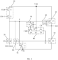
- FIG. 1 is a schematic diagram of a circuit structure of an n-th light-emitting drive sub-circuit in a light-emitting drive circuit provided by an embodiment of the present application.
- the light-emitting drive circuit provided by the embodiment of the present application may include N cascaded light-emitting drive sub-circuits, n ⁇ [1, N].
- the n-th light-emitting drive sub-circuit provided by the embodiment of the present application may include: a first pull-up control module 10, a pull-up module 20, a first pull-down control module 30, a second pull-down control module 40 and a pull-down module 50.
- An input of the first pull-up control module 10 is configured to be connected to a first power supply VDD, and a control end of the first pull-up control module 10 is configured to receive a first clock signal CKB and a (n+1)-th stage light-emitting drive signal EM+1.
- An output of the pull-up control module 10 is in electrical connection with a first node P, and the first pull-up control module 10 is configured to pull up a potential of the first node P to a first potential in a trigger phase.
- the first power supply VDD may be a DC power supply and output a high-potential voltage, and the first potential may be a high potential.
- the control end of the first pull-up control module 10 is configured to receive the first clock signal CKB and a pull-up signal.
- the pull-up signal and the first clock signal CKB jointly control the first pull-up control module 10 to be switched on, so that the potential of the first node P is pulled up to the first potential.
- a control end of the first pull-down control module 30 is configured to receive a second clock signal CK.
- An output of the first pull-down control module 30 is in electrical connection with the first node P, and the first pull-down control module 30 is configured to pull down the potential of the first node P to a second potential in an output phase, and to pull up the potential of the first node P to a third potential in a reset phase.
- a phase of the second clock signal CK is opposite to that of the first clock signal CKB, the second potential is a low potential, and the third potential is a high potential.
- An input of the pull-up module 20 is configured to be connected to the first power supply VDD, a control end of the pull-up module 20 is in electrical connection with the first node P, and an output of the pull-up module 20 is in electrical connection with a light-emitting drive-signal output.
- the pull-up module 20 is configured to pull up a n-th stage light-emitting drive signal EM output from the light-emitting drive-signal output to a high potential in a case that the potential of the first node P is the first potential or the third potential (that is, in the trigger phase or the reset phase).
- An input of the second pull-down control module 40 is configured to receive the first clock signal CKB and to be connected to the first power supply VDD respectively, and a control end of the second pull-down control module 40 is configured to be connected to the first node P and to receive the second clock signal CK respectively.
- An output of the second pull-down control module 40 is in electrical connection with a second node Q, and the second pull-down control module 40 is configured to pull up a potential of the second node Q to a fourth potential in the output phase.
- the fourth potential is a high potential.
- An input of the pull-down module 50 is configured to be connected to a second power supply VSS, a control end of the pull-down module 50 is in electrical connection with the second node Q, and an output of the pull-down module 50 is in electrical connection with the light-emitting drive-signal output.
- the pull-down module 50 is configured to pull down the n-th stage light-emitting drive signal EM output from the light-emitting drive-signal output to a low potential in a case that the potential of the second node Q is the fourth potential (that is, in the output phase).
- the second power supply VSS may be a DC power supply, and output a low-potential voltage.
- the light-emitting drive-signal output of the n-th stage light-emitting drive sub-circuit outputs the n-th stage light-emitting drive signal EM of high potential in the trigger phase and the reset phase, and outputs the n-th stage light-emitting drive signal EM of a low potential in the output phase.
- the n-th stage light-emitting drive sub-circuit is enabled to modulate a desired light-emitting control signal (that is, the n-th stage light-emitting drive signal EM) through the first pull-up control module 10, the pull-up module 20, the first pull-down control module 30, the second pull-down control module 40, the pull-down module 50 and the corresponding connection relations between the above five modules. Since only 5 modules are used, the architecture of the light-emitting drive circuit is enabled to be simplified, and thus the complexity of the light-emitting drive circuit architecture can be reduced.
- the n-th light-emitting drive sub-circuit may also include a second pull-up control module 60, one end of the second pull-up control module 60 is in electrical connection with the control end of the pull-up module 20, and the other end is in electrical connection with the light-emitting drive-signal output.
- the pull-up control module 60 is configured to pull up the potential of the first node P from the first potential to a fifth potential in the reset phase.
- the fifth potential is a high potential and is higher than the first potential.
- the pull-up module 20 may pull up the potential of the n-th stage light-emitting drive signal EM output from the light-emitting drive-signal output in a case that the potential of the first node P is the fifth potential.
- the potential of the first node P is the potential at the control end of the pull-up module 20. That is to say, the potential of the control end of the pull-up module 20 will be pulled up by the second pull-up control module 60 from the first potential to the fifth potential in the reset phase, so that the pull-up module 20 is enabled to pull up the potential of the n-th stage light-emitting drive signal EM to be closer to an ideal value (that is, the potential of the first power supply VDD).
- the n-th light-emitting drive sub-circuit may also include a first maintenance module 70 and a second maintenance module 80.
- An input of the first maintenance module 70 is configured to be connected to the second power supply VSS, a control end of the first maintenance module 70 is in electrical connection with the first node P, and an output of the first maintenance module 70 is in electrical connection with the second node Q.
- the first maintenance module 70 is enabled to maintain the low potential of the second node Q in a case that the potential of the first node P is the first potential or the fifth potential (that is, in the trigger phase), so that the pull-down module 50 continues to be switched off, and the light-emitting drive-signal output is enabled to output only the n-th stage light-emitting drive signal EM of high potential.
- An input of the second maintenance module 80 is configured to be connected to the second power supply VSS, a control end of the second maintenance module 80 is in electrical connection with the second node Q, and an output of the second maintenance module 80 is in electrical connection with the first node P.
- the second maintenance module 80 is enabled to maintain the low potential of the first node P in a case that the potential of the second node Q is the fourth potential (that is, in the output phase), so that the pull-up module 20 continues to be switched off, and the light-emitting drive-signal output is enabled to output only the n-th stage light-emitting drive signal EM of low potential.
- the n-th light-emitting drive sub-circuit may also include a current stabilization module 90, an input of the current stabilization module 90 is in electrical connection with the first node P, a control end of the current stabilization module 90 is in electrical connection with the first power supply VDD, and an output of the current stabilization module 90 is in electrical connection with the second pull-down control module 40.
- the current stabilization module 90 is enabled to stabilize a current at the control end of the pull-up module 20, so that the pull-up module 20 can pull up the potential of the n-th stage light-emitting drive signal EM in a more stable manner, and thus the n-th stage light-emitting drive signal EM output from the light-emitting drive-signal output after being pulled up is also more stable.
- the first pull-up control module 10 may include a first transistor T1 and a second transistor T2.
- a control electrode of the first transistor T1 is configured to receive the first clock signal CKB, a first electrode of the first transistor T1 is in electrical connection with the first power supply VDD, and a second electrode of the first transistor T1 is in electrical connection with a first electrode of the second transistor T2.
- a control electrode of the second transistor T2 is configured to receive the (n+1)-th stage light-emitting drive signal EM+1, and a second electrode of the second transistor T2 is in electrical connection with the first node P.
- the pull-up module 20 may include a seventh transistor T7.
- a control electrode of the seventh transistor T7 is in electrical connection with the first node P, a first electrode of the seventh transistor T7 is configured to be connected to the first power supply VDD, and a second electrode of the seventh transistor T7 is in electrical connection with the light-emitting drive-signal output.
- the first pull-down control module 30 may include an eighth transistor T8.
- a control electrode of the eighth transistor T8 is configured to receive the second clock signal CK
- a second electrode of the eighth transistor T8 is in electrical connection with the first node P.
- the second pull-down control module 40 may include a third transistor T3, a fourth transistor T4 and a second capacitor C2.
- a control electrode of the third transistor T3 is in electrical connection with the first node P, a first electrode of the third transistor T3 is configured to receive the first clock signal CKB, and a second electrode of the third transistor T3 is in electrical connection with a first electrode of the fourth transistor T4.
- a control electrode of the fourth transistor T4 is configured to receive the second clock signal CK, and a second electrode of the fourth transistor T4 is in electrical connection with the second node Q.
- One end of the second capacitor C2 is in electrical connection with the first power supply VDD, and the other end of the second capacitor C2 is in electrical connection with the second electrode of the third transistor T3.
- the pull-down module 50 may include a ninth transistor T9.
- a control electrode of the ninth transistor T9 is in electrical connection with the second node Q, a first electrode of the ninth transistor T9 is configured to be connected to the second power supply VSS, and a second electrode of the ninth transistor T9 is in electrical connection with the light-emitting drive-signal output.
- the second pull-up control module 60 may include a first capacitor C1, one end of the first capacitor C1 is in electrical connection with the control electrode of the seventh transistor T7, and the other end is in electrical connection with the light-emitting drive-signal output.
- the first maintenance module 70 may include a fifth transistor T5.
- a first electrode of the fifth transistor T5 is in electrical connection with the second power supply VSS, a control electrode of the fifth transistor T5 is in electrical connection with the first node P, and a second electrode of the fifth transistor T5 is in electrical connection with the second node Q.
- the second maintenance module 80 may include a sixth transistor T6.
- a first electrode of the sixth transistor T6 is in electrical connection with the second power supply VSS, a control electrode of the sixth transistor T6 is in electrical connection with the second node Q, and a second electrode of the sixth transistor T6 electrode is in electrical connection with the first node P.
- the current stabilization module 90 may include a tenth transistor.
- a control electrode of the tenth transistor is in electrical connection with the first power supply VDD, a first electrode of the tenth transistor is in electrical connection with the first node P, and a second electrode of the tenth transistor is in electrical connection with the control electrode of the third transistor T3.
- the first transistor T1, the second transistor T2, the fourth transistor T4 and the eighth transistor T8 may be PMOS transistors or NMOS transistors.
- a transistor is a PMOS transistor, the first electrode of the transistor is the source, the second electrode of the transistor is the drain, and the control electrode of the transistor is the gate;
- a transistor is an NMOS transistor, the first electrode of the transistor is the drain, the second electrode of the transistor is the source, and the control electrode of the transistor is the gate.
- the foregoing transistors are all NMOS transistors, as an example for exemplary illustrations.
- An embodiment of the present application also provides a method for timing control, which is applied to the above-mentioned light-emitting drive circuit.
- a second clock signal CK line is controlled to output a low-potential second clock signal CK, to enable the first pull-down control module 30 to be switched off;
- a first clock signal CKB line is controlled to output a high-potential first clock signal CKB, to enable the first pull-up control module 10 to be switched on when the (n+1)-th stage light-emitting drive signal EM+1 is at a high potential, so that the potential of the first node P is pulled up to the first potential, and the second pull-down control module 40 is charged.
- the first clock signal CKB line is controlled to output a low-potential first clock signal CKB, to enable the first pull-up control module 10 to be switched off;
- the second clock signal CK line is controlled to output a high-potential second clock signal CK, to enable the first pull-down control module 30 to be switched on, so that the second pull-down control module 40 is discharged, and the potential of the second node Q is pulled up to the fourth potential.
- the second clock signal CK line is controlled to output the high-potential second clock signal CK, to enable the first pull-down control module 30 to be switched on when the (n-1)-th stage light-emitting drive signal EM-1 is at a high potential, so that the potential of the first node P is pulled up to the third potential.
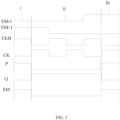
- FIG. 2 is an operation timing diagram of the light-emitting drive sub-circuit controlled by the method for timing control provided by an embodiment of the present application. As shown in FIG. 2 , in the trigger phase I, the second clock signal CK is at a low potential, and the fourth transistor T4 and the eighth transistor T8 are switched off.
- the first clock signal CKB and the (n+1)-th stage light-emitting drive signal EM+1 are at a high potential, the first transistor T1 and the second transistor T2 are switched on, the potential of the first node P is pulled up to the first potential, and the first capacitor C1 is charged, the seventh transistor T7 is switched on, the high potential of the first power supply VDD is written into the light-emitting drive-signal output via the switched-on seventh transistor T7, and the n-th stage light-emitting drive signal EM of high-potential is output from the light-emitting drive-signal output.
- the high potential of the first node P enables the third transistor T3 to be switched on, the second capacitor C2 is charged, and the high-potential first clock signal CKB is written into a node N1 via the third transistor T3, and the node N1 is maintained at a high potential to complete an action of signal temporary storage, the potential of the second node Q remains at a low potential, and the ninth transistor T9 is switched off.
- the high potential of the first node P also enables the fifth transistor T5 to be switched on, and the low potential of the second power supply VSS is written into the second node Q to maintain the low potential of the second node Q, so that the ninth transistor T9 continuous to be switched off.
- the potential of the first clock signal CKB is changed to a low potential, the first transistor T1 is switched off.
- the potential of the second clock signal CK is changed to a high potential, the eighth transistor T8 is switched on, and the (n-1)-th stage light-emitting drive signal EM-1 of low potential (that is, the second potential) is written into the first node P, the third transistor T3 and the seventh transistor T7 are switched off.
- the fourth transistor T4 is switched on, the second capacitor C2 is discharged, the high potential of the node N1 (that is, the fourth potential) is written into the second node Q, the ninth transistor T9 is switched on, and the low potential of the second power supply VSS is written into the light-emitting drive-signal output via the switched-on ninth transistor T9, and the n-th stage light-emitting drive signal EM of low potential is output from the light-emitting drive-signal output to complete a high-and-low potential switching of the n-th stage light-emitting drive signal EM.
- the high potential of the second node Q also enables the sixth transistor T6 to be switched on, the low potential of the second power supply VSS is written into the first node P to maintain the low potential of the first node P, so that the seventh transistor T7 continues to be switched off.
- the second transistor T2 continuous to be switched off, although the high and low potentials of the first clock signal CKB and the second clock signal CK are switched, and the potential of the first node P is still maintained at a low potential.
- the switching between the high and low potentials of the second clock signal CK will cause the fourth transistor T4 to switch between on and off states, the potential of the second node Q will always be maintained at a high potential. Therefore, in the entire output phase II, the n-th stage light-emitting drive signal EM of low potential will be continuously output from the light-emitting drive-signal output.
- the (n-1)-th stage light-emitting drive signal EM-1 is switched to a high potential, and as the potential of the second clock signal CK is changed to a high potential, the eighth transistor T8 is switched on, and the (n-1)-th stage light-emitting drive signal EM-1 of high potential is written into the first node P writes, and at this time, the first capacitor C1 is discharged, to enable the potential of the gate of the seventh transistor T7 to be boosted to the fifth potential, the seventh transistor T7 is switched on, and the high potential of the first power supply VDD is written into the light-emitting drive-signal output via the switched-on seventh transistor T7, and the n-th stage light-emitting drive signal EM of high potential is output from the light-emitting drive-signal output.
- the high potential of the first node P also enables the fifth transistor T5 to be switched on, the low potential of the second power supply VSS is written into the second node Q to maintain the low potential of the second node Q, and the ninth transistor T9 continues to be switched off
- An embodiment of the present application also provides a display panel, including the above-mentioned light-emitting drive circuit and a plurality of pixel drive circuits that are in connection with the light-emitting drive circuit, and the light-emitting drive circuit is configured to output a corresponding light-emitting drive signal to each pixel drive circuit.
- the circuit modules illustrated in the embodiments of the present application do not constitute a specific limitation on the pixel drive circuit.
- the pixel drive circuit may include more or fewer circuit modules than that shown in the figures, or some circuit modules may be combined, or some circuit modules may be split; each circuit module may include more or fewer devices than shown in the figures.
- the illustrated circuit modules may be implemented in hardware, software or a combination of software and hardware.
- the technical solution provided by the embodiment of the present application includes N cascaded light-emitting drive sub-circuits, and an n-th light-emitting drive sub-circuit includes: a first pull-up control module, a pull-up module, a first pull-down control module, and a second pull-down control module and a pull-down module, n ⁇ [1, N].
- An input of the first pull-up control module is configured to be connected to a first power supply
- a control end of the first pull-up control module is configured to receive a first clock signal and a (n+1)-th stage light-emitting drive signal
- an output of the first pull-up control module is in electrical connection with a first node.
- the first pull-up control module is configured to pull up a potential of the first node to a first potential in a trigger phase.
- An input of the first pull-down control module is configured to receive a (n-1)-th stage light-emitting drive signal, a control end of the first pull-down control module is configured to receive a second clock signal, and an output of the first pull-down control module is in electrical connection with the first node.
- the first pull-down control module is configured to pull down the potential of the first node a second potential in an output phase, and to pull up the potential of the first node to a third potential in a reset phase.
- An input of the pull-up module is configured to be connected to the first power supply, a control end of the pull-up module is in electrical connection with the first node, and an output of the pull-up module is in electrical connection with a light-emitting drive-signal output.
- the pull-up module is configured to pull up a n-th stage light-emitting drive-signal output from the light-emitting drive-signal output to a high potential in a case that the potential of the first node is the first potential or the third potential.
- An input of the second pull-down control module is configured to receive the first clock signal and to be connected to the first power supply, respectively, a control end of the second pull-down control module is configured to be connected to the first node and to receive the second clock signal respectively, and an output of the second pull-down control module is in electrical connection with the second node.
- the second pull-down control module is configured to pull up the potential of the second node to a fourth potential in the output phase.
- An input of the pull-down module is configured to be connected to the second power supply, a control end of the pull-down module is in electrical connection with the second node, and an output of the pull-down module is in electrical connection with the light-emitting drive-signal output.
- the pull-down module is configured to pull down the n-th stage light-emitting drive-signal output from the light-emitting drive-signal output to a low potential in a case that the potential of the second node is the fourth potential.
- the light-emitting drive sub-circuit of each stage can modulate a desired light-emitting control signal through the first pull-up control module, the pull-up module, the first pull-down control module, the second pull-down control module, the pull-down module and their corresponding connection relations, only a small number of modules is adopted, thereby the architecture of the light-emitting drive circuit can be simplified and thus the complexity of the light-emitting drive circuit architecture is reduced.
- orientations or positional relationships indicated by terms such as “central”, “longitudinal”, “transverse”, “upper”, “lower”, “front”, “rear”, “left”, “right”, “vertical”, “horizontal”, “top”, “bottom”, “inner”, “outer”, etc. are based on the orientations or positional relationships shown in the drawings, which are only used for the convenience of describing the present application and simplifying the description, rather than indicating or implying that a device or element referred to must have a particular orientation, be constructed, and operated in a particular orientation, and thus should not be construed as limiting the present application.
- the terms “installation”, “in connection with”, and “connected to” should be understood in a broad sense, for example, it may be a fixed connection, a detachable connection, or an integration; it may be a mechanical connection or an electrical connection; it may be directly connected or indirectly connected through an intermediary, and it may also be an internal communication of two components.
- a plurality of means two or more than two.
- "at least one of the following" or similar expressions refer to any combination of these items, including any combination of single items or plural items.
- at least one of a, b, or c may include that: a, b, c, a-b, a-c, b-c, or a-b-c, wherein a, b, c may be singular or plural.
- references to "one embodiment” or “some embodiments” or the like described in the specification of the present application mean that a particular feature, structure or characteristic described in connection with that embodiment is included in one or more embodiments of the present application.
- appearances of the phrases “in one embodiment,” “in some embodiments,” “in other embodiments,” “in some other embodiments,” etc. in various places in this specification are not necessarily all refer to the same embodiment, but mean “one or more but not all embodiments” unless specifically stated otherwise.
Landscapes
- Engineering & Computer Science (AREA)
- Physics & Mathematics (AREA)
- Computer Hardware Design (AREA)
- General Physics & Mathematics (AREA)
- Theoretical Computer Science (AREA)
- Control Of Indicators Other Than Cathode Ray Tubes (AREA)
- Control Of El Displays (AREA)
Abstract
Description
- This application claims priority to
Chinese Patent Application No. 202310197985.0, filed with the China National Intellectual Property Administration on March 03, 2023 - The present application relates to the field of display technologies, and in particular, to a light-emitting drive circuit, a method for timing control, and a display panel.
- Light-emitting devices, such as an organic light-emitting diode (Organic Light Emitting Diode, OLED), due to their characteristics such as, thin and lightness, energy efficient, wide color gamut and high contrast, have gradually been widely used in televisions, mobile phones, notebooks and other products.
- The OLED, when being an active-driven emitting-light device, usually requires a light-emitting drive circuit to provide a corresponding light-emitting control signal, in addition to requiring a row-scanning drive circuit to provide a corresponding scanning signal.
- However, circuit configurations of the current light-emitting drive circuits are complicated, and more modules or components are required to realize a control of the light-emitting control signal.
- One objective of embodiments of the present application is to provide a light-emitting drive circuit, a method for timing control, and a display panel, aiming to solve the problem that more modules or components are required to realize the control of the light-emitting control signal due to the complex circuit configurations in current light-emitting drive circuits.
- To achieve the above objective, in accordance with a first aspect, an embodiment of the present application provides a light-emitting drive circuit, which includes: N cascaded light-emitting drive sub-circuits, and an n-th light-emitting drive sub-circuit includes: a first pull-up control module, a pull-up module, a first pull-down control module, a second pull-down control module and a pull-down module, where, n ∈ [1, N].
- An input of the first pull-up control module is configured to be connected to a first power supply, a control end of the first pull-up control module is configured to receive a first clock signal and a (n+1)-th stage light-emitting drive signal, and an output of the first pull-up control module is in electrical connection with a first node. The first pull-up control module is configured to pull up a potential of the first node to a first potential in a trigger phase.
- An input of the first pull-down control module is configured to receive a (n-1)-th stage light-emitting drive signal, a control end of the first pull-down control module is configured to receive a second clock signal, and an output of the first pull-down control module is in electrical connection with the first node. The first pull-down control module is configured to pull down the potential of the first node to a second potential in an output phase and to pull up the potential of the first node to a third potential in a reset phase.
- An input of the pull-up module is configured to be connected to the first power supply, a control end of the pull-up module is in electrical connection with a first node, and an output of the pull-up module is in electrical connection with a light-emitting drive-signal output. The pull-up module is configured to pull up a n-th stage light-emitting drive-signal output from the light-emitting drive-signal output to a high potential in a case that a potential of the first node is the first potential or the third potential.
- An input of the second pull-down control module is configured to receive the first clock signal and to be connected to the first power supply respectively, a control end of the second pull-down control module is configured to be connected to the first node and receive the second clock signal respectively, and an output of the second pull-down control module is in electrical connection with a second node. The second pull-down control module is configured to pull up a potential of the second node to a fourth potential in the output phase.
- An input of the pull-down module is configured to be connected to a second power supply, a control end of the pull-down module is in electrical connection with the second node, and an output of the pull-down module is in electrical connection with the light-emitting drive-signal output. The pull-down module is configured to pull down the n-th stage light-emitting drive-signal output from the light-emitting drive-signal output to a low potential in a case that the potential of the second node is the fourth potential.
- As an optional implementation of the embodiment of the present application, the n-th light-emitting drive sub-circuit further includes a second pull-up control module.
- One end of the second pull-up control module is in electrical connection with the control end of the pull-up module, and an opposite end of the second pull-up control module is in electrical connection with the light-emitting drive-signal output. The second pull-up control module is configured to pull up the potential of the first node from the first potential to a fifth potential in the reset phase, and the pull-up module is configured to pull up a potential of the n-th stage light-emitting drive-signal output from the light-emitting drive-signal output in a case that the potential of the first node is the fifth potential.
- As an optional implementation of the embodiment of the present application, the n-th light-emitting drive sub-circuit further includes a second pull-up control module.
- One end of the second pull-up control module is in electrical connection with the control end of the pull-up module, and an opposite end of the second pull-up control module is in electrical connection with the light-emitting drive-signal output. The second pull-up control module is configured to pull up the potential of the first node from the first potential to a fifth potential in the reset phase, and the pull-up module is configured to pull up a potential of the n-th stage light-emitting drive-signal output from the light-emitting drive-signal output in a case that the potential of the first node is the fifth potential.
- As an optional implementation of the embodiment of the present application, the second pull-up control module includes a first capacitor, one end of the first capacitor is in electrical connection with the control end of the pull-up module, and the other end is in electrical connection with the light-emitting drive-signal output.
- As an optional implementation of the embodiment of the present application, the first pull-up control module includes: a first transistor and a second transistor.
- A control electrode of the first transistor is configured to receive the first clock signal, a first electrode of the first transistor is in electrical connection with the first power supply, and a second electrode of the first transistor is in electrical connection with a first electrode of the second transistor.
- A control electrode of the second transistor is configured to receive the (n+1)-th stage light-emitting drive signal, and a second electrode of the second transistor is in electrical connection with the first node.
- As an optional implementation of the embodiment of the present application, the second pull-down control module includes: a third transistor, a fourth transistor, and a second capacitor.
- A control electrode of the third transistor is in electrical connection with the first node, a first electrode of the third transistor is configured to receive the first clock signal, a second electrode of the third transistor is in electrical connection with a first electrode of the fourth transistor.
- A control electrode of the fourth transistor is configured to receive the second clock signal, and a second electrode of the fourth transistor is in electrical connection with the second node.
- One end of the second capacitor is in electrical connection with the first power supply, and an opposite end of the second capacitor is in electrical connection with the second electrode of the third transistor.
- As an optional implementation of the embodiment of the present application, the n-th light-emitting drive sub-circuit further includes: a first maintenance module and a second maintenance module.
- An input of the first maintenance module is configured to be connected to the second power supply, a control end of the first maintenance module is in electrical connection with the first node, and an output of the first maintenance module is in electrical connection with the second node. The first maintenance module is configured to maintain the potential of the second node in a case that the potential of the first node is the first potential.
- An input of the second maintenance module is configured to be connected to the second power supply, a control end of the second maintenance module is in electrical connection with the second node, and an output of the second maintenance module is in electrical connection with the first node. The second maintenance module is configured to maintain the potential of the first node in a case that the potential of the second node is the fourth potential.
- As an optional implementation of the embodiment of the present application, the first maintenance module includes a fifth transistor, a first electrode of the fifth transistor is in electrical connection with the second power supply, a control electrode of the fifth transistor is in electrical connection with the first node, and a second electrode of the fifth transistor is in electrical connection with the second node.
- As an optional implementation of the embodiment of the present application, the second maintenance module includes a sixth transistor, a first electrode of the sixth transistor is in electrical connection with the second power supply, a control electrode of the sixth transistor is in electrical connection with the second node, and a second electrode of the sixth transistor is in electrical connection with the first node.
- As an optional implementation of the embodiment of the present application, the pull-up module includes a seventh transistor, a control electrode of the seventh transistor is in electrical connection with the first node, a first electrode of the seventh transistor is configured to be connected to the first power supply, and a second electrode of the seventh transistor is in electrical connection with the light-emitting drive-signal output.
- As an optional implementation of the embodiment of the present application, the first pull-down control module includes an eighth transistor, a control electrode of the eighth transistor is configured to receive the second clock signal, a first electrode of the eighth transistor is configured to receive the (n-1)-th stage light-emitting drive signal, and a second electrode of the eighth transistor is in electrical connection with the first node.
- As an optional implementation of the embodiment of the present application, the pull-down module includes a ninth transistor, a control electrode of the ninth transistor is in electrical connection with the second node, a first electrode of the ninth transistor is configured to be connected to the second power supply, and a second electrode of the ninth transistor is in electrical connection with the light-emitting drive-signal output.
- As an optional implementation of the embodiment of the present application, the n-th light-emitting drive sub-circuit further includes a current stabilization module.
- An input of the current stabilization module is in electrical connection with the first node, a control end of the current stabilization module is in electrical connection with the first power supply, and an output of the current stabilization module is in electrical connection with the control end of the second pull-down control module. The current stabilization module is configured to stabilize a current at the control end of the pull-up module.
- As an optional implementation of the embodiment of the present application, the current stabilization module includes a tenth transistor, a control electrode of the tenth transistor is in electrical connection with the first power supply, a first electrode of the tenth transistor is in electrical connection with the first node, and a second electrode of the tenth transistor is in electrical connection with the control end of the second pull-down control module
- In accordance with a second aspect, an embodiment of the present application provides a method for timing control, which is applied to the light-emitting drive circuit according to the first aspect or any one of the first aspect, and the method includes the following phases.
- In a trigger phase, a second clock signal line is controlled to output a low-potential second clock signal, to enable the first pull-down control module to be switched off; a first clock signal line is controlled to output a high-potential first clock signal, to enable the first pull-up control module to be switched on when the (n+1)-th stage light-emitting drive signal is at a high potential, so that the potential of the first node is pulled up to the first potential, and the second pull-down control module is charged.
- In an output phase, the first clock signal line is controlled to output a low-potential first clock signal, to enable the first pull-up control module to be switched off; the second clock signal line is controlled to output a high-potential second clock signal, to enable the first pull-down control module to be switched on, so that the second pull-down control module is discharged, and the potential of the second node is pulled up to the fourth potential.
- In a reset phase, the second clock signal line is controlled to output the high-potential second clock signal, to enable the first pull-down control module to be switched on when the (n-1)-th stage light-emitting drive signal is at a high potential, so that the potential of the first node is pulled up to the third potential.
- In accordance with a third aspect, an embodiment of the present application provides a display panel, including the light-emitting drive circuit described in the first aspect or any one of the first aspect and a plurality of pixel drive circuits connected to the light-emitting drive circuit. The light-emitting drive circuit is configured to output corresponding light-emitting drive signals to each of the pixel drive circuits.
- The technical solution provided by the embodiment of the present application includes N cascaded light-emitting drive sub-circuits, and an n-th light-emitting drive sub-circuit includes: a first pull-up control module, a pull-up module, a first pull-down control module, and a second pull-down control module and a pull-down module, n ∈ [1, N]. An input of the first pull-up control module is configured to be connected to a first power supply, a control end of the first pull-up control module is configured to receive a first clock signal and a (n+1)-th stage light-emitting drive signal, and an output of the first pull-up control module is in electrical connection with a first node. The first pull-up control module is configured to pull up a potential of the first node to a first potential in a trigger phase. An input of the first pull-down control module is configured to receive a (n-1)-th stage light-emitting drive signal, a control end of the first pull-down control module is configured to receive a second clock signal, and an output of the first pull-down control module is in electrical connection with the first node. The first pull-down control module is configured to pull down the potential of the first node to a second potential in an output phase, and to pull up the potential of the first node to a third potential in a reset phase. An input of the pull-up module is configured to be connected to the first power supply, a control end of the pull-up module is in electrical connection with the first node, and an output of the pull-up module is in electrical connection with a light-emitting drive-signal output. The pull-up module is configured to pull up a n-th stage light-emitting drive-signal output from the light-emitting drive-signal output to a high potential in a case that the potential of the first node is the first potential or the third potential. An input of the second pull-down control module is configured to receive the first clock signal and to be connected to the first power supply, respectively, a control end of the second pull-down control module is configured to be connected to the first node and to receive the second clock signal respectively, and an output of the second pull-down control module is in electrical connection with the second node. The second pull-down control module is configured to pull up the potential of the second node to a fourth potential in the output phase. An input of the pull-down module is configured to be connected to the second power supply, a control end of the pull-down module is in electrical connection with the second node, and an output of the pull-down module is in electrical connection with the light-emitting drive-signal output. The pull-down module is configured to pull down the n-th stage light-emitting drive-signal output from the light-emitting drive-signal output to a low potential in a case that the potential of the second node is the fourth potential. In the above solution, each of the cascaded light-emitting drive sub-circuit can modulate a desired light-emitting control signal through the first pull-up control module, the pull-up module, the first pull-down control module, the second pull-down control module, the pull-down module and the corresponding connectivity among these modules, only a small number of modules is adopted, thereby the configuration of the light-emitting drive circuit can be simplified and thus the complexity of the circuit configuration of the light-emitting drive circuit is reduced.
- In order to illustrate the solutions in the embodiments of the present application more clearly, a brief description of the drawings required for use in the description of the embodiments will be given below. It will be apparent that the drawings in the following description are only some embodiments of the present application, and for persons of ordinary skill in the art, other drawings may also be obtained on the basis of these drawings without exerting any creative effort.
-
FIG. 1 is a schematic diagram of a circuit structure of an n-th light-emitting drive sub-circuit in a light-emitting drive circuit provided by an embodiment of the present application; and -
FIG. 2 is an operation timing diagram of the light-emitting drive sub-circuit controlled by a method for timing control provided by an embodiment of the present application. - In order to make the objectives, solutions and advantages of the present application more comprehensible, the implementations of the present application will be further described in detail below in conjunction with the drawings.
- The terms used in implementations of the embodiments of the present application are only used to explain the specific embodiments of the present application, and are not intended to limit the present application. The following specific embodiments may be combined with each other, and the same or similar concepts or processes may not be repeated in some embodiments.
- The light-emitting device in the embodiments of the present application may be any one of an OLED, a quantum dot light-emitting diode (Quantum Dot Light Emitting Diodes, QLED) and a sub-millimeter light-emitting diode (Mini Light Emitting Diodes, Mini LED). In the following, the embodiment will take the OLED as an example for exemplary description.
-
FIG. 1 is a schematic diagram of a circuit structure of an n-th light-emitting drive sub-circuit in a light-emitting drive circuit provided by an embodiment of the present application. The light-emitting drive circuit provided by the embodiment of the present application may include N cascaded light-emitting drive sub-circuits, n ∈ [1, N]. As shown inFIG. 1 , the n-th light-emitting drive sub-circuit provided by the embodiment of the present application may include: a first pull-upcontrol module 10, a pull-upmodule 20, a first pull-down control module 30, a second pull-down control module 40 and a pull-down module 50. - An input of the first pull-up
control module 10 is configured to be connected to a first power supply VDD, and a control end of the first pull-upcontrol module 10 is configured to receive a first clock signal CKB and a (n+1)-th stage light-emitting drive signal EM+1. An output of the pull-upcontrol module 10 is in electrical connection with a first node P, and the first pull-upcontrol module 10 is configured to pull up a potential of the first node P to a first potential in a trigger phase. The first power supply VDD may be a DC power supply and output a high-potential voltage, and the first potential may be a high potential. - It can be understood that when n=N, the control end of the first pull-up
control module 10 is configured to receive the first clock signal CKB and a pull-up signal. The pull-up signal and the first clock signal CKB jointly control the first pull-upcontrol module 10 to be switched on, so that the potential of the first node P is pulled up to the first potential. - An input of the first pull-
down control module 30 is configured to receive a (n-1)-th stage light-emitting drive signal EM-1 (when n=1, the input of the first pull-down control module 30 is configured to receive a start signal STE). A control end of the first pull-down control module 30 is configured to receive a second clock signal CK. An output of the first pull-down control module 30 is in electrical connection with the first node P, and the first pull-down control module 30 is configured to pull down the potential of the first node P to a second potential in an output phase, and to pull up the potential of the first node P to a third potential in a reset phase. A phase of the second clock signal CK is opposite to that of the first clock signal CKB, the second potential is a low potential, and the third potential is a high potential. - An input of the pull-up
module 20 is configured to be connected to the first power supply VDD, a control end of the pull-upmodule 20 is in electrical connection with the first node P, and an output of the pull-upmodule 20 is in electrical connection with a light-emitting drive-signal output. The pull-upmodule 20 is configured to pull up a n-th stage light-emitting drive signal EM output from the light-emitting drive-signal output to a high potential in a case that the potential of the first node P is the first potential or the third potential (that is, in the trigger phase or the reset phase). - An input of the second pull-
down control module 40 is configured to receive the the first clock signal CKB and to be connected to the first power supply VDD respectively, and a control end of the second pull-down control module 40 is configured to be connected to the first node P and to receive the second clock signal CK respectively. An output of the second pull-down control module 40 is in electrical connection with a second node Q, and the second pull-down control module 40 is configured to pull up a potential of the second node Q to a fourth potential in the output phase. The fourth potential is a high potential. - An input of the pull-
down module 50 is configured to be connected to a second power supply VSS, a control end of the pull-down module 50 is in electrical connection with the second node Q, and an output of the pull-down module 50 is in electrical connection with the light-emitting drive-signal output. The pull-down module 50 is configured to pull down the n-th stage light-emitting drive signal EM output from the light-emitting drive-signal output to a low potential in a case that the potential of the second node Q is the fourth potential (that is, in the output phase). The second power supply VSS may be a DC power supply, and output a low-potential voltage. - The light-emitting drive-signal output of the n-th stage light-emitting drive sub-circuit outputs the n-th stage light-emitting drive signal EM of high potential in the trigger phase and the reset phase, and outputs the n-th stage light-emitting drive signal EM of a low potential in the output phase. In this way, the n-th stage light-emitting drive sub-circuit is enabled to modulate a desired light-emitting control signal (that is, the n-th stage light-emitting drive signal EM) through the first pull-up
control module 10, the pull-upmodule 20, the first pull-down control module 30, the second pull-down control module 40, the pull-down module 50 and the corresponding connection relations between the above five modules. Since only 5 modules are used, the architecture of the light-emitting drive circuit is enabled to be simplified, and thus the complexity of the light-emitting drive circuit architecture can be reduced. - The n-th light-emitting drive sub-circuit may also include a second pull-up
control module 60, one end of the second pull-upcontrol module 60 is in electrical connection with the control end of the pull-upmodule 20, and the other end is in electrical connection with the light-emitting drive-signal output. The pull-upcontrol module 60 is configured to pull up the potential of the first node P from the first potential to a fifth potential in the reset phase. The fifth potential is a high potential and is higher than the first potential. The pull-upmodule 20 may pull up the potential of the n-th stage light-emitting drive signal EM output from the light-emitting drive-signal output in a case that the potential of the first node P is the fifth potential. Since the first node P is in electrical connection with the control end of the pull-upmodule 20, the potential of the first node P is the potential at the control end of the pull-upmodule 20. That is to say, the potential of the control end of the pull-upmodule 20 will be pulled up by the second pull-upcontrol module 60 from the first potential to the fifth potential in the reset phase, so that the pull-upmodule 20 is enabled to pull up the potential of the n-th stage light-emitting drive signal EM to be closer to an ideal value (that is, the potential of the first power supply VDD). - The n-th light-emitting drive sub-circuit may also include a
first maintenance module 70 and asecond maintenance module 80. An input of thefirst maintenance module 70 is configured to be connected to the second power supply VSS, a control end of thefirst maintenance module 70 is in electrical connection with the first node P, and an output of thefirst maintenance module 70 is in electrical connection with the second node Q. Thefirst maintenance module 70 is enabled to maintain the low potential of the second node Q in a case that the potential of the first node P is the first potential or the fifth potential (that is, in the trigger phase), so that the pull-down module 50 continues to be switched off, and the light-emitting drive-signal output is enabled to output only the n-th stage light-emitting drive signal EM of high potential. - An input of the
second maintenance module 80 is configured to be connected to the second power supply VSS, a control end of thesecond maintenance module 80 is in electrical connection with the second node Q, and an output of thesecond maintenance module 80 is in electrical connection with the first node P. Thesecond maintenance module 80 is enabled to maintain the low potential of the first node P in a case that the potential of the second node Q is the fourth potential (that is, in the output phase), so that the pull-upmodule 20 continues to be switched off, and the light-emitting drive-signal output is enabled to output only the n-th stage light-emitting drive signal EM of low potential. - The n-th light-emitting drive sub-circuit may also include a
current stabilization module 90, an input of thecurrent stabilization module 90 is in electrical connection with the first node P, a control end of thecurrent stabilization module 90 is in electrical connection with the first power supply VDD, and an output of thecurrent stabilization module 90 is in electrical connection with the second pull-down control module 40. Thecurrent stabilization module 90 is enabled to stabilize a current at the control end of the pull-upmodule 20, so that the pull-upmodule 20 can pull up the potential of the n-th stage light-emitting drive signal EM in a more stable manner, and thus the n-th stage light-emitting drive signal EM output from the light-emitting drive-signal output after being pulled up is also more stable. - To be specific, the first pull-up
control module 10 may include a first transistor T1 and a second transistor T2. A control electrode of the first transistor T1 is configured to receive the first clock signal CKB, a first electrode of the first transistor T1 is in electrical connection with the first power supply VDD, and a second electrode of the first transistor T1 is in electrical connection with a first electrode of the second transistor T2. - A control electrode of the second transistor T2 is configured to receive the (n+1)-th stage light-emitting drive signal EM+1, and a second electrode of the second transistor T2 is in electrical connection with the first node P.
- The pull-up
module 20 may include a seventh transistor T7. A control electrode of the seventh transistor T7 is in electrical connection with the first node P, a first electrode of the seventh transistor T7 is configured to be connected to the first power supply VDD, and a second electrode of the seventh transistor T7 is in electrical connection with the light-emitting drive-signal output. - The first pull-
down control module 30 may include an eighth transistor T8. A control electrode of the eighth transistor T8 is configured to receive the second clock signal CK, a first electrode of the eighth transistor T8 is configured to receive the (n-1)-th stage light-emitting drive signal EM-1 (When n=1, the first electrode of the eighth transistor T8 is configured to receive the start signal STE), and a second electrode of the eighth transistor T8 is in electrical connection with the first node P. - The second pull-
down control module 40 may include a third transistor T3, a fourth transistor T4 and a second capacitor C2. A control electrode of the third transistor T3 is in electrical connection with the first node P, a first electrode of the third transistor T3 is configured to receive the first clock signal CKB, and a second electrode of the third transistor T3 is in electrical connection with a first electrode of the fourth transistor T4. - A control electrode of the fourth transistor T4 is configured to receive the second clock signal CK, and a second electrode of the fourth transistor T4 is in electrical connection with the second node Q.
- One end of the second capacitor C2 is in electrical connection with the first power supply VDD, and the other end of the second capacitor C2 is in electrical connection with the second electrode of the third transistor T3.
- The pull-
down module 50 may include a ninth transistor T9. A control electrode of the ninth transistor T9 is in electrical connection with the second node Q, a first electrode of the ninth transistor T9 is configured to be connected to the second power supply VSS, and a second electrode of the ninth transistor T9 is in electrical connection with the light-emitting drive-signal output. - The second pull-up
control module 60 may include a first capacitor C1, one end of the first capacitor C1 is in electrical connection with the control electrode of the seventh transistor T7, and the other end is in electrical connection with the light-emitting drive-signal output. - The
first maintenance module 70 may include a fifth transistor T5. A first electrode of the fifth transistor T5 is in electrical connection with the second power supply VSS, a control electrode of the fifth transistor T5 is in electrical connection with the first node P, and a second electrode of the fifth transistor T5 is in electrical connection with the second node Q. - The
second maintenance module 80 may include a sixth transistor T6. A first electrode of the sixth transistor T6 is in electrical connection with the second power supply VSS, a control electrode of the sixth transistor T6 is in electrical connection with the second node Q, and a second electrode of the sixth transistor T6 electrode is in electrical connection with the first node P. - The
current stabilization module 90 may include a tenth transistor. A control electrode of the tenth transistor is in electrical connection with the first power supply VDD, a first electrode of the tenth transistor is in electrical connection with the first node P, and a second electrode of the tenth transistor is in electrical connection with the control electrode of the third transistor T3. - The first transistor T1, the second transistor T2, the fourth transistor T4 and the eighth transistor T8 may be PMOS transistors or NMOS transistors. When a transistor is a PMOS transistor, the first electrode of the transistor is the source, the second electrode of the transistor is the drain, and the control electrode of the transistor is the gate; when a transistor is an NMOS transistor, the first electrode of the transistor is the drain, the second electrode of the transistor is the source, and the control electrode of the transistor is the gate. In this embodiment, the foregoing transistors are all NMOS transistors, as an example for exemplary illustrations.
- An embodiment of the present application also provides a method for timing control, which is applied to the above-mentioned light-emitting drive circuit. In the trigger phase, a second clock signal CK line is controlled to output a low-potential second clock signal CK, to enable the first pull-
down control module 30 to be switched off; a first clock signal CKB line is controlled to output a high-potential first clock signal CKB, to enable the first pull-upcontrol module 10 to be switched on when the (n+1)-th stage light-emitting drive signal EM+1 is at a high potential, so that the potential of the first node P is pulled up to the first potential, and the second pull-down control module 40 is charged. - In the output phase, the first clock signal CKB line is controlled to output a low-potential first clock signal CKB, to enable the first pull-up
control module 10 to be switched off; the second clock signal CK line is controlled to output a high-potential second clock signal CK, to enable the first pull-down control module 30 to be switched on, so that the second pull-down control module 40 is discharged, and the potential of the second node Q is pulled up to the fourth potential. - In the reset phase, the second clock signal CK line is controlled to output the high-potential second clock signal CK, to enable the first pull-
down control module 30 to be switched on when the (n-1)-th stage light-emitting drive signal EM-1 is at a high potential, so that the potential of the first node P is pulled up to the third potential. -
FIG. 2 is an operation timing diagram of the light-emitting drive sub-circuit controlled by the method for timing control provided by an embodiment of the present application. As shown inFIG. 2 , in the trigger phase I, the second clock signal CK is at a low potential, and the fourth transistor T4 and the eighth transistor T8 are switched off. The first clock signal CKB and the (n+1)-th stage light-emitting drive signal EM+1 are at a high potential, the first transistor T1 and the second transistor T2 are switched on, the potential of the first node P is pulled up to the first potential, and the first capacitor C1 is charged, the seventh transistor T7 is switched on, the high potential of the first power supply VDD is written into the light-emitting drive-signal output via the switched-on seventh transistor T7, and the n-th stage light-emitting drive signal EM of high-potential is output from the light-emitting drive-signal output. At the same time, the high potential of the first node P enables the third transistor T3 to be switched on, the second capacitor C2 is charged, and the high-potential first clock signal CKB is written into a node N1 via the third transistor T3, and the node N1 is maintained at a high potential to complete an action of signal temporary storage, the potential of the second node Q remains at a low potential, and the ninth transistor T9 is switched off. In addition, the high potential of the first node P also enables the fifth transistor T5 to be switched on, and the low potential of the second power supply VSS is written into the second node Q to maintain the low potential of the second node Q, so that the ninth transistor T9 continuous to be switched off. - At the beginning of the output phase II, the potential of the first clock signal CKB is changed to a low potential, the first transistor T1 is switched off. The potential of the second clock signal CK is changed to a high potential, the eighth transistor T8 is switched on, and the (n-1)-th stage light-emitting drive signal EM-1 of low potential (that is, the second potential) is written into the first node P, the third transistor T3 and the seventh transistor T7 are switched off. The fourth transistor T4 is switched on, the second capacitor C2 is discharged, the high potential of the node N1 (that is, the fourth potential) is written into the second node Q, the ninth transistor T9 is switched on, and the low potential of the second power supply VSS is written into the light-emitting drive-signal output via the switched-on ninth transistor T9, and the n-th stage light-emitting drive signal EM of low potential is output from the light-emitting drive-signal output to complete a high-and-low potential switching of the n-th stage light-emitting drive signal EM. In addition, the high potential of the second node Q also enables the sixth transistor T6 to be switched on, the low potential of the second power supply VSS is written into the first node P to maintain the low potential of the first node P, so that the seventh transistor T7 continues to be switched off.
- In the subsequent period of the output phase II, since the (n-1)-th stage light-emitting drive signal EM-1 and the (n+1)-th stage light-emitting drive signal EM+1 are at low potential, the second transistor T2 continuous to be switched off, although the high and low potentials of the first clock signal CKB and the second clock signal CK are switched, and the potential of the first node P is still maintained at a low potential. Moreover, although the switching between the high and low potentials of the second clock signal CK will cause the fourth transistor T4 to switch between on and off states, the potential of the second node Q will always be maintained at a high potential. Therefore, in the entire output phase II, the n-th stage light-emitting drive signal EM of low potential will be continuously output from the light-emitting drive-signal output.
- In the reset phase III, the (n-1)-th stage light-emitting drive signal EM-1 is switched to a high potential, and as the potential of the second clock signal CK is changed to a high potential, the eighth transistor T8 is switched on, and the (n-1)-th stage light-emitting drive signal EM-1 of high potential is written into the first node P writes, and at this time, the first capacitor C1 is discharged, to enable the potential of the gate of the seventh transistor T7 to be boosted to the fifth potential, the seventh transistor T7 is switched on, and the high potential of the first power supply VDD is written into the light-emitting drive-signal output via the switched-on seventh transistor T7, and the n-th stage light-emitting drive signal EM of high potential is output from the light-emitting drive-signal output. In addition, the high potential of the first node P also enables the fifth transistor T5 to be switched on, the low potential of the second power supply VSS is written into the second node Q to maintain the low potential of the second node Q, and the ninth transistor T9 continues to be switched off
- An embodiment of the present application also provides a display panel, including the above-mentioned light-emitting drive circuit and a plurality of pixel drive circuits that are in connection with the light-emitting drive circuit, and the light-emitting drive circuit is configured to output a corresponding light-emitting drive signal to each pixel drive circuit.
- It can be understood that the circuit modules illustrated in the embodiments of the present application do not constitute a specific limitation on the pixel drive circuit. In other embodiments of the present application, the pixel drive circuit may include more or fewer circuit modules than that shown in the figures, or some circuit modules may be combined, or some circuit modules may be split; each circuit module may include more or fewer devices than shown in the figures. The illustrated circuit modules may be implemented in hardware, software or a combination of software and hardware.
- The technical solution provided by the embodiment of the present application includes N cascaded light-emitting drive sub-circuits, and an n-th light-emitting drive sub-circuit includes: a first pull-up control module, a pull-up module, a first pull-down control module, and a second pull-down control module and a pull-down module, n ∈ [1, N]. An input of the first pull-up control module is configured to be connected to a first power supply, a control end of the first pull-up control module is configured to receive a first clock signal and a (n+1)-th stage light-emitting drive signal, and an output of the first pull-up control module is in electrical connection with a first node. The first pull-up control module is configured to pull up a potential of the first node to a first potential in a trigger phase. An input of the first pull-down control module is configured to receive a (n-1)-th stage light-emitting drive signal, a control end of the first pull-down control module is configured to receive a second clock signal, and an output of the first pull-down control module is in electrical connection with the first node. The first pull-down control module is configured to pull down the potential of the first node a second potential in an output phase, and to pull up the potential of the first node to a third potential in a reset phase. An input of the pull-up module is configured to be connected to the first power supply, a control end of the pull-up module is in electrical connection with the first node, and an output of the pull-up module is in electrical connection with a light-emitting drive-signal output. The pull-up module is configured to pull up a n-th stage light-emitting drive-signal output from the light-emitting drive-signal output to a high potential in a case that the potential of the first node is the first potential or the third potential. An input of the second pull-down control module is configured to receive the first clock signal and to be connected to the first power supply, respectively, a control end of the second pull-down control module is configured to be connected to the first node and to receive the second clock signal respectively, and an output of the second pull-down control module is in electrical connection with the second node. The second pull-down control module is configured to pull up the potential of the second node to a fourth potential in the output phase. An input of the pull-down module is configured to be connected to the second power supply, a control end of the pull-down module is in electrical connection with the second node, and an output of the pull-down module is in electrical connection with the light-emitting drive-signal output. The pull-down module is configured to pull down the n-th stage light-emitting drive-signal output from the light-emitting drive-signal output to a low potential in a case that the potential of the second node is the fourth potential. In the above solution, the light-emitting drive sub-circuit of each stage can modulate a desired light-emitting control signal through the first pull-up control module, the pull-up module, the first pull-down control module, the second pull-down control module, the pull-down module and their corresponding connection relations, only a small number of modules is adopted, thereby the architecture of the light-emitting drive circuit can be simplified and thus the complexity of the light-emitting drive circuit architecture is reduced.
- In the above embodiments, the descriptions of each embodiment have their own emphases, and for parts that are not detailed or recorded in a certain embodiment, references may be made to the relevant descriptions of other embodiments.
- In addition, the size ratio relationship among the various components in the drawings is only schematic, which may not necessarily reflect the actual size ratio relationship between the various components.
- In the description of this application, orientations or positional relationships indicated by terms such as "central", "longitudinal", "transverse", "upper", "lower", "front", "rear", "left", "right", "vertical", "horizontal", "top", "bottom", "inner", "outer", etc., are based on the orientations or positional relationships shown in the drawings, which are only used for the convenience of describing the present application and simplifying the description, rather than indicating or implying that a device or element referred to must have a particular orientation, be constructed, and operated in a particular orientation, and thus should not be construed as limiting the present application.
- In the description of the present application, it should be noted that unless otherwise specified and limited, the terms "installation", "in connection with", and "connected to" should be understood in a broad sense, for example, it may be a fixed connection, a detachable connection, or an integration; it may be a mechanical connection or an electrical connection; it may be directly connected or indirectly connected through an intermediary, and it may also be an internal communication of two components. Those of ordinary skills in the art can understand the specific meanings of the above terms in the present application based on specific situations.
- It should be understood that the term "comprising", when used in the specification and claims of the present application, indicates a presence of described features, integers, steps, operations, elements and/or components, but does not exclude the presence or addition of one or more other features, wholes, steps, operations, elements, components and/or combinations thereof.
- In the description of the present application, unless otherwise specified, "/" means that the objects associated with each other are an "or" relationship, for example, A/B may mean A or B. the expression "and/or" in the present application is only an association relationship describing associated objects, which means that three kinds of relationships may be included, for example, A and/or B, may include three cases, that is, A exists alone, both A and B exist, and B exists alone, among which A, B C may be singular or plural.
- In addition, in the description of the present application, unless otherwise specified, the phrase "a plurality of" means two or more than two. "at least one of the following" or similar expressions refer to any combination of these items, including any combination of single items or plural items. For example, at least one of a, b, or c may include that: a, b, c, a-b, a-c, b-c, or a-b-c, wherein a, b, c may be singular or plural.
- In addition, in the description of the specification and the appended claims of the present application, the terms "first", "second", "third" and so on are used to distinguish similar objects, and are not necessarily used to describe a specific order or sequence order. It should be understood that the terms used in this way are interchangeable under appropriate circumstances such that the embodiments described herein can be practiced in other orders other than those illustrated or described herein.
- References to "one embodiment" or "some embodiments" or the like described in the specification of the present application mean that a particular feature, structure or characteristic described in connection with that embodiment is included in one or more embodiments of the present application. Thus, appearances of the phrases "in one embodiment," "in some embodiments," "in other embodiments," "in some other embodiments," etc. in various places in this specification are not necessarily all refer to the same embodiment, but mean "one or more but not all embodiments" unless specifically stated otherwise.
- Finally, it should be noted that: the above embodiments are only used to illustrate the technical solutions of the present application, and are not intended to limit the present application. Although the present application has been described in detail with reference to the foregoing embodiments, those of ordinary skills in the art should understand that the technical solutions described in the foregoing embodiments may still be modified, or some or all of the technical features thereof may be equivalently replaced; and these modifications or replacements do not make the essence of the corresponding technical solutions to deviate from the scope of the technical solutions of the various embodiments of the present application.
Claims (15)
- A light-emitting drive circuit, characterized by comprising: N cascaded light-emitting drive sub-circuits, and an n-th light-emitting drive sub-circuit comprising: a first pull-up control module, a pull-up module, a first pull-down control module, a second pull-down control module, and a pull-down module, wherein, n ∈ [1, N];wherein an input of the first pull-up control module is configured to be connected to a first power supply, a control end of the first pull-up control module is configured to receive a first clock signal and a (n+1)-th stage light-emitting drive signal, an output of the first pull-up control module is in electrical connection with a first node, and the first pull-up control module is configured to pull up a potential of the first node to a first potential in a trigger phase;wherein an input of the first pull-down control module is configured to receive a (n-1)-th stage light-emitting drive signal, a control end of the first pull-down control module is configured to receive a second clock signal, an output of the first pull-down control module is in electrical connection with the first node, and the first pull-down control module is configured to pull down the potential of the first node to a second potential in an output phase and to pull up the potential of the first node to a third potential in a reset phase;wherein an input of the pull-up module is configured to be connected to the first power supply, a control end of the pull-up module is in electrical connection with a first node, an output of the pull-up module is in electrical connection with a light-emitting drive-signal output, and the pull-up module is configured to pull up a n-th stage light-emitting drive-signal output from the light-emitting drive-signal output to a high potential in a case that a potential of the first node is the first potential or the third potential;wherein an input of the second pull-down control module is configured to receive the first clock signal and to be connected to the first power supply respectively, a control end of the second pull-down control module is configured to be connected to the first node and to receive the second clock signal respectively, an output of the second pull-down control module is in electrical connection with a second node, and the second pull-down control module is configured to pull up a potential of the second node to a fourth potential in the output phase; andwherein an input of the pull-down module is configured to be connected to a second power supply, a control end of the pull-down module is in electrical connection with the second node, an output of the pull-down module is in electrical connection with the light-emitting drive-signal output, and the pull-down module is configured to pull down the n-th stage light-emitting drive-signal output from the light-emitting drive-signal output to a low potential in a case that the potential of the second node is the fourth potential.
- The light-emitting drive circuit according to claim 1, characterized in that, the n-th light-emitting drive sub-circuit further comprises:
a second pull-up control module, one end of the second pull-up control module is in electrical connection with the control end of the pull-up module, and an opposite end of the second pull-up control module is in electrical connection with the light-emitting drive-signal output, and the second pull-up control module is configured to pull up the potential of the first node from the first potential to a fifth potential in the reset phase, and the pull-up module is configured to pull up a potential of the n-th stage light-emitting drive-signal output from the light-emitting drive-signal output in a case that the potential of the first node is the fifth potential. - The light-emitting drive circuit according to claim 2, characterized in that, the second pull-up control module comprises a first capacitor, one end of the first capacitor is in electrical connection with the control end of the pull-up module, and an opposite end of the first capacitor is in electrical connection with the light-emitting drive-signal output.
- The light-emitting drive circuit according to claim 1, characterized in that, the first pull-up control module comprises: a first transistor and a second transistor;a control electrode of the first transistor is configured to receive the first clock signal, a first electrode of the first transistor is in electrical connection with the first power supply, and a second electrode of the first transistor is in electrical connection with a first electrode of the second transistor; anda control electrode of the second transistor is configured to receive the (n+1)-th stage light-emitting drive signal, and a second electrode of the second transistor is in electrical connection with the first node.
- The light-emitting drive circuit according to claim 1, characterized in that, the second pull-down control module comprises: a third transistor, a fourth transistor and a second capacitor;a control electrode of the third transistor is in electrical connection with the first node, a first electrode of the third transistor is configured to receive the first clock signal, a second electrode of the third transistor is in electrical connection with a first electrode of the fourth transistor;a control electrode of the fourth transistor is configured to receive the second clock signal, and a second electrode of the fourth transistor is in electrical connection with the second node; andone end of the second capacitor is in electrical connection with the first power supply, and an opposite end of the second capacitor is in electrical connection with the second electrode of the third transistor.
- The light-emitting drive circuit according to claim 1, characterized in that, the n-th light-emitting drive sub-circuit further comprises:a first maintenance module, an input of the first maintenance module is configured to be connected to the second power supply, a control end of the first maintenance module is in electrical connection with the first node, an output of the first maintenance module is in electrical connection with the second node, and the first maintenance module is configured to maintain the potential of the second node in a case that the potential of the first node is the first potential; anda second maintenance module, an input of the second maintenance module is configured to be connected to the second power supply, a control end of the second maintenance module is in electrical connection with the second node, an output of the second maintenance module is in electrical connection with the first node, and the second maintenance module is configured to maintain the potential of the first node in a case that the potential of the second node is the fourth potential.
- The light-emitting drive circuit according to claim 6, characterized in that, the first maintenance module comprises a fifth transistor, a first electrode of the fifth transistor is in electrical connection with the second power supply, a control electrode of the fifth transistor is in electrical connection with the first node, and a second electrode of the fifth transistor is in electrical connection with the second node.
- The light-emitting drive circuit according to claim 6, characterized in that, the second maintenance module comprises a sixth transistor, a first electrode of the sixth transistor is in electrical connection with the second power supply, a control electrode of the sixth transistor is in electrical connection with the second node, and a second electrode of the sixth transistor is in electrical connection with the first node.
- The light-emitting drive circuit according to claim 1, characterized in that, the pull-up module comprises a seventh transistor, a control electrode of the seventh transistor is in electrical connection with the first node, a first electrode of the seventh transistor is configured to be connected to the first power supply, and a second electrode of the seventh transistor is in electrical connection with the light-emitting drive-signal output.
- The light-emitting drive circuit according to claim 1, characterized in that, the first pull-down control module comprises an eighth transistor, a control electrode of the eighth transistor is configured to receive the second clock signal, a first electrode of the eighth transistor is configured to receive the (n-1)-th stage light-emitting drive signal, and a second electrode of the eighth transistor is in electrical connection with the first node.
- The light-emitting drive circuit according to claim 1, characterized in that, the pull-down module comprises a ninth transistor, a control electrode of the ninth transistor is in electrical connection with the second node, a first electrode of the ninth transistor is configured to be connected to the second power supply, and a second electrode of the ninth transistor is in electrical connection with the light-emitting drive-signal output.
- The light-emitting drive circuit according to any one of claims 1-11, characterized in that, the n-th light-emitting drive sub-circuit further comprises:
a current stabilization module, an input of the current stabilization module is in electrical connection with the first node, a control end of the current stabilization module is in electrical connection with the first power supply, an output of the current stabilization module is in electrical connection with the control end of the second pull-down control module, and the current stabilization module is configured to stabilize a current at the control end of the pull-up module. - The light-emitting drive circuit according to claim 12, characterized in that, the current stabilization module comprises a tenth transistor, a control electrode of the tenth transistor is in electrical connection with the first power supply, a first electrode of the tenth transistor is in electrical connection with the first node, and a second electrode of the tenth transistor is in electrical connection with the control end of the second pull-down control module.
- A method for timing control, characterized in that, the method is applied to the light-emitting drive circuit according to any one of claims 1-13, and the method comprises:in a trigger phase, controlling a second clock signal line to output a low-potential second clock signal, enabling the first pull-down control module to be switched off; controlling a first clock signal line to output a high-potential first clock signal, enabling the first pull-up control module to be switched on when the (n+1)-th stage light-emitting drive signal is at a high potential, pulling up the potential of the first node to the first potential, and charging the second pull-down control module;in an output phase, controlling the first clock signal line to output a low-potential first clock signal, enabling the first pull-up control module to be switched off; controlling the second clock signal line to output a high-potential second clock signal, enabling the first pull-down control module to be switched on, discharging the second pull-down control module, and the pulling up potential of the second node to the fourth potential; andin a reset phase, controlling the second clock signal line to output a high-potential second clock signal, enabling the first pull-down control module to be switched on when the (n-1)-th stage light-emitting drive signal is at a high potential, pulling up the potential of the first node to the third potential.
- A display panel, characterized by comprising: the light-emitting drive circuit according to any one of claims 1-13; and a plurality of pixel drive circuits, connected to the light-emitting drive circuit, wherein the light-emitting drive circuit is configured to output corresponding light-emitting drive signals to the plurality of pixel drive circuits.
Applications Claiming Priority (2)
| Application Number | Priority Date | Filing Date | Title |
|---|---|---|---|
| CN202310197985.0A CN115881038B (en) | 2023-03-03 | 2023-03-03 | Light-emitting driving circuit, timing control method and display panel |
| PCT/CN2023/098100 WO2024183174A1 (en) | 2023-03-03 | 2023-06-02 | Light-emitting drive circuit, timing control method, and display panel |
Publications (2)
| Publication Number | Publication Date |
|---|---|
| EP4451256A1 true EP4451256A1 (en) | 2024-10-23 |
| EP4451256A4 EP4451256A4 (en) | 2024-12-18 |
Family
ID=85761924
Family Applications (1)
| Application Number | Title | Priority Date | Filing Date |
|---|---|---|---|
| EP23904832.5A Pending EP4451256A4 (en) | 2023-03-03 | 2023-06-02 | LIGHT-EMITTING DRIVER CIRCUIT, TIME CONTROL METHOD AND DISPLAY BOARD |
Country Status (6)
| Country | Link |
|---|---|
| US (1) | US11967275B1 (en) |
| EP (1) | EP4451256A4 (en) |
| JP (1) | JP7708505B2 (en) |
| KR (1) | KR20250067910A (en) |
| CN (1) | CN115881038B (en) |
| WO (1) | WO2024183174A1 (en) |
Families Citing this family (3)
| Publication number | Priority date | Publication date | Assignee | Title |
|---|---|---|---|---|
| CN115881038B (en) * | 2023-03-03 | 2023-06-09 | 惠科股份有限公司 | Light-emitting driving circuit, timing control method and display panel |
| CN116504184B (en) * | 2023-06-30 | 2023-09-15 | 惠科股份有限公司 | Light-emitting driving circuit, time sequence control method and display panel |
| CN121096274B (en) * | 2025-11-10 | 2026-02-10 | 惠科股份有限公司 | Drive circuit, display panel and display device |
Family Cites Families (36)
| Publication number | Priority date | Publication date | Assignee | Title |
|---|---|---|---|---|
| KR101544052B1 (en) * | 2009-02-11 | 2015-08-13 | 삼성디스플레이 주식회사 | Gate driving circuit and display device having the gate driving circuit |
| KR101752834B1 (en) * | 2009-12-29 | 2017-07-03 | 삼성디스플레이 주식회사 | Gate driving circuit and display apparatus having the same |
| KR101170241B1 (en) * | 2010-06-03 | 2012-07-31 | 하이디스 테크놀로지 주식회사 | Driving circuit for electric paper display and display device |
| CN103943081A (en) * | 2014-03-14 | 2014-07-23 | 京东方科技集团股份有限公司 | Shifting register, manufacturing method of shifting register, grid line integrated drive circuit and relevant devices |
| CN104157259B (en) * | 2014-09-10 | 2016-06-22 | 深圳市华星光电技术有限公司 | Gate driver circuit based on IGZO processing procedure |
| KR102307678B1 (en) * | 2014-12-03 | 2021-10-01 | 엘지디스플레이 주식회사 | Emitting control signal driver of display device and method of driving the same, And Organic Light Emitting Display Device |
| CN104392704A (en) * | 2014-12-15 | 2015-03-04 | 合肥京东方光电科技有限公司 | Shifting register unit and driving method thereof, shifting register and display device |
| CN105118414B (en) * | 2015-09-17 | 2017-07-28 | 京东方科技集团股份有限公司 | Shift register and its driving method, gate driving circuit, display device |
| KR102579690B1 (en) * | 2016-02-29 | 2023-09-19 | 삼성디스플레이 주식회사 | Gate driver and display apparatus including the same |
| KR102582032B1 (en) * | 2016-04-05 | 2023-09-25 | 삼성디스플레이 주식회사 | Emissioin driver and display device including the same |
| KR102477486B1 (en) * | 2016-04-19 | 2022-12-14 | 삼성디스플레이 주식회사 | Emission control driver and display device having the same |
| CN106205520B (en) * | 2016-07-08 | 2018-10-30 | 京东方科技集团股份有限公司 | Shift register, grid line integrated drive electronics, array substrate and display device |
| CN106128364B (en) * | 2016-07-15 | 2018-12-11 | 京东方科技集团股份有限公司 | Shift register cell and its driving method, gate driving circuit, display device |
| CN106297697B (en) * | 2016-08-29 | 2017-09-15 | 京东方科技集团股份有限公司 | Shift register and its operating method |
| CN106486078B (en) * | 2016-12-30 | 2019-05-03 | 深圳市华星光电技术有限公司 | A kind of scan drive circuit, driving circuit and display device |
| CN107154236B (en) * | 2017-07-24 | 2020-01-17 | 京东方科技集团股份有限公司 | Shift register unit and driving method thereof, scan driving circuit and display device |
| KR102567324B1 (en) * | 2017-08-30 | 2023-08-16 | 엘지디스플레이 주식회사 | Gate driver and display device including the same |
| CN108597431A (en) * | 2018-02-12 | 2018-09-28 | 京东方科技集团股份有限公司 | Shift register cell and its control method, gate driving circuit, display device |
| CN108538336B (en) * | 2018-04-19 | 2020-12-15 | 上海天马有机发光显示技术有限公司 | Light-emitting shift register and light-emitting control method, driving circuit and display device |
| CN108682397A (en) * | 2018-07-27 | 2018-10-19 | 京东方科技集团股份有限公司 | Shift register cell, gate driving circuit, display device and driving method |
| CN110335572B (en) * | 2019-06-27 | 2021-10-01 | 重庆惠科金渝光电科技有限公司 | Array substrate row driving circuit unit, driving circuit thereof and liquid crystal display panel |
| CN111415695B (en) * | 2020-03-16 | 2022-06-21 | 京东方科技集团股份有限公司 | Shift register, grid driving circuit and display control method |
| KR102756390B1 (en) * | 2020-06-29 | 2025-01-21 | 삼성디스플레이 주식회사 | Stage and display device including the same |
| CN112017591A (en) * | 2020-08-31 | 2020-12-01 | 南京中电熊猫液晶显示科技有限公司 | Emission control drive circuit and organic light emitting display device |
| KR102943052B1 (en) * | 2021-03-29 | 2026-03-25 | 삼성디스플레이 주식회사 | Display device |
| KR102841501B1 (en) * | 2021-04-12 | 2025-08-05 | 삼성디스플레이 주식회사 | Electronic device and operating method of the same |
| CN113113071B (en) * | 2021-04-13 | 2024-09-13 | 京东方科技集团股份有限公司 | Shift register unit and driving method thereof, gate driving circuit, and display device |
| CN113257205B (en) * | 2021-05-18 | 2023-02-03 | 武汉华星光电技术有限公司 | Grid driving circuit and display panel |
| CN114067729B (en) * | 2021-11-16 | 2022-10-04 | 武汉华星光电技术有限公司 | Light-emitting drive circuit and display panel |
| CN114038417B (en) * | 2021-11-22 | 2023-05-05 | Tcl华星光电技术有限公司 | Light-emitting control signal generation circuit and OLED display panel |
| CN114299848B (en) * | 2021-12-30 | 2023-07-25 | 武汉天马微电子有限公司 | Display panel and display device |
| CN114613335B (en) * | 2022-03-11 | 2023-10-03 | Tcl华星光电技术有限公司 | Gate drive circuit and display panel |
| CN114974062B (en) * | 2022-04-24 | 2024-10-18 | 京东方科技集团股份有限公司 | A gate driving circuit and driving method thereof, and a display device |
| CN114974163B (en) * | 2022-06-28 | 2023-05-26 | 惠科股份有限公司 | Scanning driving circuit, array substrate and display panel |
| CN115148166B (en) * | 2022-06-30 | 2024-05-24 | 惠科股份有限公司 | Scanning driving circuit, array substrate and display panel |
| CN115881038B (en) * | 2023-03-03 | 2023-06-09 | 惠科股份有限公司 | Light-emitting driving circuit, timing control method and display panel |
-
2023
- 2023-03-03 CN CN202310197985.0A patent/CN115881038B/en active Active
- 2023-06-02 JP JP2024539655A patent/JP7708505B2/en active Active
- 2023-06-02 KR KR1020257012119A patent/KR20250067910A/en active Pending
- 2023-06-02 WO PCT/CN2023/098100 patent/WO2024183174A1/en not_active Ceased
- 2023-06-02 EP EP23904832.5A patent/EP4451256A4/en active Pending
- 2023-07-14 US US18/352,483 patent/US11967275B1/en active Active
Also Published As
| Publication number | Publication date |
|---|---|
| WO2024183174A1 (en) | 2024-09-12 |
| US11967275B1 (en) | 2024-04-23 |
| JP2025512211A (en) | 2025-04-17 |
| JP7708505B2 (en) | 2025-07-15 |
| EP4451256A4 (en) | 2024-12-18 |
| KR20250067910A (en) | 2025-05-15 |
| CN115881038A (en) | 2023-03-31 |
| CN115881038B (en) | 2023-06-09 |
Similar Documents
| Publication | Publication Date | Title |
|---|---|---|
| US11967275B1 (en) | Light-emitting drive circuit, method for timing control, and display panel | |
| US11763740B2 (en) | Signal generation circuit, signal generation method, signal generation module and display device | |
| CN111243519B (en) | Light emission control signal generation circuit, display panel, and display device | |
| US9997101B2 (en) | Gate scan circuit, driving method thereof and gate scan cascade circuit | |
| US10964268B2 (en) | Scan driving circuit, driving method, and display device | |
| US10769977B2 (en) | Shift register and driving method of the same, emission driving circuit, and display device | |
| EP3236459B1 (en) | Scanning drive circuit and display device | |
| CN113113071B (en) | Shift register unit and driving method thereof, gate driving circuit, and display device | |
| US10726778B2 (en) | Emission driving circuit, driving method of the same, and display device | |
| US10891902B2 (en) | Driving circuit of display device | |
| US8723765B2 (en) | Stage circuit and scan driver using the same | |
| CN112820234B (en) | Shift register circuit and display device | |
| US11335228B1 (en) | Scanning signal circuit, display panel, display device, and driving method | |
| US12488753B2 (en) | Display panel and display device | |
| CN116504184B (en) | Light-emitting driving circuit, time sequence control method and display panel | |
| US12361881B2 (en) | Display panel and display device | |
| US12236896B2 (en) | Display panel and electronic apparatus | |
| EP3624103A1 (en) | Emission control driving circuit, emission control driver and organic light emitting display device | |
| CN114999365B (en) | Scan driving circuit and display panel | |
| CN112509512A (en) | GIP circuit and driving method | |
| CN119920199A (en) | Gate drive circuit and display panel | |
| CN213958558U (en) | GIP circuit | |
| CN111261108A (en) | Gate drive circuit | |
| CN119446070B (en) | Display driving circuit, display panel and display equipment | |
| CN120108317A (en) | Shift register unit and driving method thereof, display driving circuit, and display device |
Legal Events
| Date | Code | Title | Description |
|---|---|---|---|
| STAA | Information on the status of an ep patent application or granted ep patent |
Free format text: STATUS: UNKNOWN |
|
| STAA | Information on the status of an ep patent application or granted ep patent |
Free format text: STATUS: THE INTERNATIONAL PUBLICATION HAS BEEN MADE |
|
| PUAI | Public reference made under article 153(3) epc to a published international application that has entered the european phase |
Free format text: ORIGINAL CODE: 0009012 |
|
| STAA | Information on the status of an ep patent application or granted ep patent |
Free format text: STATUS: REQUEST FOR EXAMINATION WAS MADE |
|
| 17P | Request for examination filed |
Effective date: 20240628 |
|
| AK | Designated contracting states |
Kind code of ref document: A1 Designated state(s): AL AT BE BG CH CY CZ DE DK EE ES FI FR GB GR HR HU IE IS IT LI LT LU LV MC ME MK MT NL NO PL PT RO RS SE SI SK SM TR |
|
| A4 | Supplementary search report drawn up and despatched |
Effective date: 20241115 |
|
| RIC1 | Information provided on ipc code assigned before grant |
Ipc: G09G 3/3208 20160101AFI20241111BHEP |
|
| STAA | Information on the status of an ep patent application or granted ep patent |
Free format text: STATUS: EXAMINATION IS IN PROGRESS |
|
| 17Q | First examination report despatched |
Effective date: 20250804 |