EP4447125A1 - Back-contact solar cell and production method therefor, and cell assembly - Google Patents
Back-contact solar cell and production method therefor, and cell assembly Download PDFInfo
- Publication number
- EP4447125A1 EP4447125A1 EP22919883.3A EP22919883A EP4447125A1 EP 4447125 A1 EP4447125 A1 EP 4447125A1 EP 22919883 A EP22919883 A EP 22919883A EP 4447125 A1 EP4447125 A1 EP 4447125A1
- Authority
- EP
- European Patent Office
- Prior art keywords
- silicon substrate
- solar cell
- contact solar
- semiconductor layer
- layer
- Prior art date
- Legal status (The legal status is an assumption and is not a legal conclusion. Google has not performed a legal analysis and makes no representation as to the accuracy of the status listed.)
- Granted
Links
Images



Classifications
-
- H—ELECTRICITY
- H10—SEMICONDUCTOR DEVICES; ELECTRIC SOLID-STATE DEVICES NOT OTHERWISE PROVIDED FOR
- H10F—INORGANIC SEMICONDUCTOR DEVICES SENSITIVE TO INFRARED RADIATION, LIGHT, ELECTROMAGNETIC RADIATION OF SHORTER WAVELENGTH OR CORPUSCULAR RADIATION
- H10F77/00—Constructional details of devices covered by this subclass
- H10F77/20—Electrodes
- H10F77/206—Electrodes for devices having potential barriers
- H10F77/211—Electrodes for devices having potential barriers for photovoltaic cells
- H10F77/219—Arrangements for electrodes of back-contact photovoltaic cells
-
- H—ELECTRICITY
- H10—SEMICONDUCTOR DEVICES; ELECTRIC SOLID-STATE DEVICES NOT OTHERWISE PROVIDED FOR
- H10F—INORGANIC SEMICONDUCTOR DEVICES SENSITIVE TO INFRARED RADIATION, LIGHT, ELECTROMAGNETIC RADIATION OF SHORTER WAVELENGTH OR CORPUSCULAR RADIATION
- H10F10/00—Individual photovoltaic cells, e.g. solar cells
- H10F10/10—Individual photovoltaic cells, e.g. solar cells having potential barriers
- H10F10/16—Photovoltaic cells having only PN heterojunction potential barriers
- H10F10/164—Photovoltaic cells having only PN heterojunction potential barriers comprising heterojunctions with Group IV materials, e.g. ITO/Si or GaAs/SiGe photovoltaic cells
- H10F10/165—Photovoltaic cells having only PN heterojunction potential barriers comprising heterojunctions with Group IV materials, e.g. ITO/Si or GaAs/SiGe photovoltaic cells the heterojunctions being Group IV-IV heterojunctions, e.g. Si/Ge, SiGe/Si or Si/SiC photovoltaic cells
- H10F10/166—Photovoltaic cells having only PN heterojunction potential barriers comprising heterojunctions with Group IV materials, e.g. ITO/Si or GaAs/SiGe photovoltaic cells the heterojunctions being Group IV-IV heterojunctions, e.g. Si/Ge, SiGe/Si or Si/SiC photovoltaic cells the Group IV-IV heterojunctions being heterojunctions of crystalline and amorphous materials, e.g. silicon heterojunction [SHJ] photovoltaic cells
-
- H—ELECTRICITY
- H10—SEMICONDUCTOR DEVICES; ELECTRIC SOLID-STATE DEVICES NOT OTHERWISE PROVIDED FOR
- H10F—INORGANIC SEMICONDUCTOR DEVICES SENSITIVE TO INFRARED RADIATION, LIGHT, ELECTROMAGNETIC RADIATION OF SHORTER WAVELENGTH OR CORPUSCULAR RADIATION
- H10F19/00—Integrated devices, or assemblies of multiple devices, comprising at least one photovoltaic cell covered by group H10F10/00, e.g. photovoltaic modules
-
- H—ELECTRICITY
- H10—SEMICONDUCTOR DEVICES; ELECTRIC SOLID-STATE DEVICES NOT OTHERWISE PROVIDED FOR
- H10F—INORGANIC SEMICONDUCTOR DEVICES SENSITIVE TO INFRARED RADIATION, LIGHT, ELECTROMAGNETIC RADIATION OF SHORTER WAVELENGTH OR CORPUSCULAR RADIATION
- H10F71/00—Manufacture or treatment of devices covered by this subclass
-
- H—ELECTRICITY
- H10—SEMICONDUCTOR DEVICES; ELECTRIC SOLID-STATE DEVICES NOT OTHERWISE PROVIDED FOR
- H10F—INORGANIC SEMICONDUCTOR DEVICES SENSITIVE TO INFRARED RADIATION, LIGHT, ELECTROMAGNETIC RADIATION OF SHORTER WAVELENGTH OR CORPUSCULAR RADIATION
- H10F71/00—Manufacture or treatment of devices covered by this subclass
- H10F71/138—Manufacture of transparent electrodes, e.g. transparent conductive oxides [TCO] or indium tin oxide [ITO] electrodes
-
- H—ELECTRICITY
- H10—SEMICONDUCTOR DEVICES; ELECTRIC SOLID-STATE DEVICES NOT OTHERWISE PROVIDED FOR
- H10F—INORGANIC SEMICONDUCTOR DEVICES SENSITIVE TO INFRARED RADIATION, LIGHT, ELECTROMAGNETIC RADIATION OF SHORTER WAVELENGTH OR CORPUSCULAR RADIATION
- H10F77/00—Constructional details of devices covered by this subclass
- H10F77/20—Electrodes
-
- H—ELECTRICITY
- H10—SEMICONDUCTOR DEVICES; ELECTRIC SOLID-STATE DEVICES NOT OTHERWISE PROVIDED FOR
- H10F—INORGANIC SEMICONDUCTOR DEVICES SENSITIVE TO INFRARED RADIATION, LIGHT, ELECTROMAGNETIC RADIATION OF SHORTER WAVELENGTH OR CORPUSCULAR RADIATION
- H10F77/00—Constructional details of devices covered by this subclass
- H10F77/20—Electrodes
- H10F77/244—Electrodes made of transparent conductive layers, e.g. transparent conductive oxide [TCO] layers
-
- H—ELECTRICITY
- H10—SEMICONDUCTOR DEVICES; ELECTRIC SOLID-STATE DEVICES NOT OTHERWISE PROVIDED FOR
- H10F—INORGANIC SEMICONDUCTOR DEVICES SENSITIVE TO INFRARED RADIATION, LIGHT, ELECTROMAGNETIC RADIATION OF SHORTER WAVELENGTH OR CORPUSCULAR RADIATION
- H10F77/00—Constructional details of devices covered by this subclass
- H10F77/30—Coatings
-
- H—ELECTRICITY
- H10—SEMICONDUCTOR DEVICES; ELECTRIC SOLID-STATE DEVICES NOT OTHERWISE PROVIDED FOR
- H10F—INORGANIC SEMICONDUCTOR DEVICES SENSITIVE TO INFRARED RADIATION, LIGHT, ELECTROMAGNETIC RADIATION OF SHORTER WAVELENGTH OR CORPUSCULAR RADIATION
- H10F77/00—Constructional details of devices covered by this subclass
- H10F77/30—Coatings
- H10F77/306—Coatings for devices having potential barriers
- H10F77/311—Coatings for devices having potential barriers for photovoltaic cells
-
- H—ELECTRICITY
- H10—SEMICONDUCTOR DEVICES; ELECTRIC SOLID-STATE DEVICES NOT OTHERWISE PROVIDED FOR
- H10F—INORGANIC SEMICONDUCTOR DEVICES SENSITIVE TO INFRARED RADIATION, LIGHT, ELECTROMAGNETIC RADIATION OF SHORTER WAVELENGTH OR CORPUSCULAR RADIATION
- H10F77/00—Constructional details of devices covered by this subclass
- H10F77/30—Coatings
- H10F77/306—Coatings for devices having potential barriers
- H10F77/311—Coatings for devices having potential barriers for photovoltaic cells
- H10F77/315—Coatings for devices having potential barriers for photovoltaic cells the coatings being antireflective or having enhancing optical properties
-
- H—ELECTRICITY
- H10—SEMICONDUCTOR DEVICES; ELECTRIC SOLID-STATE DEVICES NOT OTHERWISE PROVIDED FOR
- H10F—INORGANIC SEMICONDUCTOR DEVICES SENSITIVE TO INFRARED RADIATION, LIGHT, ELECTROMAGNETIC RADIATION OF SHORTER WAVELENGTH OR CORPUSCULAR RADIATION
- H10F77/00—Constructional details of devices covered by this subclass
- H10F77/40—Optical elements or arrangements
- H10F77/42—Optical elements or arrangements directly associated or integrated with photovoltaic cells, e.g. light-reflecting means or light-concentrating means
- H10F77/488—Reflecting light-concentrating means, e.g. parabolic mirrors or concentrators using total internal reflection
-
- H—ELECTRICITY
- H10—SEMICONDUCTOR DEVICES; ELECTRIC SOLID-STATE DEVICES NOT OTHERWISE PROVIDED FOR
- H10F—INORGANIC SEMICONDUCTOR DEVICES SENSITIVE TO INFRARED RADIATION, LIGHT, ELECTROMAGNETIC RADIATION OF SHORTER WAVELENGTH OR CORPUSCULAR RADIATION
- H10F77/00—Constructional details of devices covered by this subclass
- H10F77/70—Surface textures, e.g. pyramid structures
- H10F77/703—Surface textures, e.g. pyramid structures of the semiconductor bodies, e.g. textured active layers
Definitions
- the present invention relates to the field of solar-cell technologies, and in particular, to a back-contact solar cell, a manufacturing method therefor, and a solar-cell assembly.
- Back-contact solar cells have a wide application prospect due to a high open-circuit voltage and a high short-circuit current.
- semiconductor layers of different doping types are arranged immediately adjacent to each other, and consequently, a short circuit easily occurs in the cell.
- the present disclosure provides a back-contact solar cell, a manufacturing method therefor, and a solar-cell assembly, to resolve a problem of a short circuit in an existing back-contact solar cell.
- a back-contact solar cell including: a solar-cell body, where the solar-cell body includes a silicon substrate, a first semiconductor layer located in a first region of a back surface of the silicon substrate, a blocking layer stacked on an end region of the first semiconductor layer, a second semiconductor layer stacked on the blocking layer and a second region of the back surface of the silicon substrate, and a transparent conductive film layer stacked on the first semiconductor layer and the second semiconductor layer.
- the first region and the second region are arranged immediately adjacent to each other.
- a doping type of the first semiconductor layer is different from a doping type of the second semiconductor layer.
- a separation groove is provided on the second semiconductor layer and the transparent conductive film layer. An area of a cross section of the separation groove decreases toward the silicon substrate. A cross section of the separation groove is parallel to the silicon substrate.
- the separation groove is provided on the second semiconductor layer and the transparent conductive film layer, to physically separate the first semiconductor layer and the second semiconductor layer with different doping types, so that the back-contact solar cell has a better insulation effect, and a problem of a short circuit is avoided.
- the cross section of the separation groove is parallel to the silicon substrate, and the area of the cross section of the separation groove decreases toward the silicon substrate, so that light incident from a light receiving surface of the silicon substrate can be incident at each position of the separation groove, and the light incident at each position of the separation groove is reflected and reaches the silicon substrate.
- an intensity of the light incident at the silicon substrate is higher, so that power of electricity generated by the back-contact solar cell is increased, photoelectric conversion efficiency of the back-contact solar cell is improved, and an open-circuit voltage and a short-circuit current of the back-contact solar cell are further increased.
- a width of the cross section of the separation groove decreases toward the silicon substrate, and a direction of the width of the cross section of the separation groove is parallel to a direction along which the first region and the second region are arranged.
- a refractive index of the transparent conductive film layer and a refractive index of the second semiconductor layer are both greater than a refractive index of the blocking layer.
- the separation groove is filled with an insulating material.
- the insulating material is light-permeable.
- the insulating material protrudes from the separation groove in a direction away from the silicon substrate.
- the insulating material protruding from the separation groove forms a hat-like structure.
- the hat-like structure includes a brim part and a crown part. An area of any cross section of the brim part is greater than an area of any cross section of the crown part.
- the brim part is closer to the separation groove.
- the area of each cross section of the brim part increases toward the silicon substrate.
- An area of a cross section of an end of the brim part close to the silicon substrate is greater than or equal to an area of a cross section of an end of the separation groove away from the silicon substrate.
- the cross sections are all parallel to the silicon substrate.
- each cross section of the brim part increases toward the silicon substrate.
- a width of a cross section of an end of the brim part close to the separation groove is greater than or equal to a width of the cross section of the end of the separation groove away from the silicon substrate.
- a direction of the width of the cross section of the brim part is parallel to a direction along which the first region and the second region are arranged.
- a refractive index of the insulating material is less than a refractive index of the blocking layer.
- the refractive index of the blocking layer is less than both a refractive index of the transparent conductive film layer and a refractive index of the second semiconductor layer.
- the refractive index of the insulating material ranges from 0.05 to 1.7
- the refractive index of the transparent conductive film layer ranges from 1.86 to 4.9
- the refractive index of the second semiconductor layer ranges from 1.86 to 4.9
- the refractive index of the blocking layer ranges from 1.85 to 2.1.
- the separation groove includes a first groove portion on the second semiconductor layer and a second groove portion on the transparent conductive film layer.
- a groove wall of the first groove portion includes a planar surface and/or a curvilinear surface; and/or a groove wall of the second groove portion includes a planar surface and/or a curvilinear surface.
- the groove wall of the first groove portion is a planar surface
- the groove wall of the second groove portion is a planar surface
- the groove wall of the first groove portion and the groove wall of the second groove portion are distributed in a step shape, or the groove wall of the first groove portion forms a smooth transition with the groove wall of the second groove portion.
- the groove wall of the first groove portion is a curvilinear surface
- the groove wall of the second groove portion is a curvilinear surface
- the curvilinear surface of the groove wall of the first groove portion and the curvilinear surface of the groove wall of the second groove portion have a same curvature.
- the insulating material exactly fits a groove wall of the separation groove.
- the insulating material includes an insulating ink and/or an insulating resin.
- the solar-cell body further includes a back surface on the blocking layer and a first passivation layer in the second region of the back surface of the silicon substrate.
- the first passivation layer is located between the second semiconductor layer and the silicon substrate.
- a refractive index of the first passivation layer is greater than the refractive index of the blocking layer.
- the separation groove is formed through the first passivation layer, the second semiconductor layer, and the transparent conductive film layer.
- a width of a cross section of an end of the separation groove close to the silicon substrate ranges from 10 ⁇ m to 80 ⁇ m, and the width of the cross section of the end of the separation groove away from the silicon substrate ranges from 20 ⁇ m to 90 ⁇ m.
- a width of a cross section of an end of the brim part close to the silicon substrate ranges from 30 ⁇ m to 120 ⁇ m.
- a width of a cross section of an end of the brim part away from the silicon substrate ranges from 20 ⁇ m to 110 ⁇ m.
- the cross section of the end of the separation groove close to the silicon substrate is parallel to the silicon substrate.
- a direction of the width of the cross section of the end of the separation groove close to the silicon substrate is parallel to the direction along which the first region and the second region are arranged.
- the back-contact solar cell further includes a first electrode and a second electrode.
- the first electrode is located in a region of the transparent conductive film layer opposite to the first semiconductor layer.
- the second electrode is located in a region of the transparent conductive film layer opposite to the second semiconductor layer.
- the hat-like structure is located between the first electrode and the second electrode, and an end of the hat-like structure away from the silicon substrate protrudes out of the first electrode and the second electrode.
- a height by which the hat-like structure protrudes out of the first electrode ranges from 0.1 ⁇ m to 50 ⁇ m.
- a direction of the height is parallel to a stacking direction of the first semiconductor layer and the silicon substrate.
- a height of the blocking layer ranges from 100 nm to 500 nm, and a direction of the height is parallel to a stacking direction of the first semiconductor layer and the silicon substrate.
- the first region does not overlap the second region.
- the silicon substrate is an N-type silicon substrate
- the first semiconductor layer is a P-type doped microcrystalline silicon layer
- the second semiconductor layer is an N+ doped amorphous silicon layer
- the blocking layer is a silicon nitride blocking layer
- the first passivation layer is an amorphous silicon layer.
- the first passivation layer is further distributed in the first region of the back surface of the silicon substrate, and the first passivation layer is located between the first semiconductor layer and the silicon substrate.
- the back-contact solar cell further includes an amorphous silicon passivation layer on a light receiving surface of the silicon substrate, and a silicon nitride anti-reflection layer on a light receiving surface of the amorphous silicon passivation layer; and/or the light receiving surface of the silicon substrate has a textured structure.
- a method for manufacturing a back-contact solar cell is further provided.
- the method is for manufacturing any one of the back-contact solar cells described above.
- the separation groove is formed on the second semiconductor layer and the transparent conductive film layer by using a Gaussian beam.
- a wavelength of the Gaussian beam ranges from 900 nm to 1200 nm, and an energy density of the Gaussian beam ranges from 0.1 J/cm 2 to 0.5 J/cm 2 .
- the method further includes: printing an insulating material in the separation groove.
- a solar-cell assembly is further provided, including any one of the back-contact solar cells described above.
- a back-contact solar cell may be an IBC solar cell (interdigitated back-contact solar cell), an HBC solar cell (heterojunction interdigitated back-contact solar cell), or the like. This is not specifically limited in the embodiments of the present invention.
- FIG. 1 is a schematic diagram of a partial structure of a first type of back-contact solar cell according to an embodiment of the present invention. As shown in FIG. 1 , the back-contact solar cell includes a solar-cell body. The solar-cell body includes a silicon substrate 1. A doping type of the silicon substrate 1 is not specifically limited. A light receiving surface of the silicon substrate 1 is a surface of the silicon substrate 1 in the back-contact solar cell that receives light.
- a back surface of the silicon substrate 1 is a surface of the silicon substrate 1 that is opposite to the light receiving surface.
- the solar-cell body further includes a first semiconductor layer 2 located in a first region of the back surface of the silicon substrate 1, a blocking layer 3 stacked on an end region of the first semiconductor layer 2, a second semiconductor layer 4 stacked on the blocking layer 3 and a second region of the back surface of the silicon substrate 1, and a transparent conductive film layer 5 stacked on the first semiconductor layer 2 and the second semiconductor layer 4.
- the end region of the first semiconductor layer 2 may be an area that is on the first semiconductor layer 2 and that is close to an end of the second semiconductor layer 4.
- a relative size of the end region relative to the first semiconductor layer 2 is not specifically limited.
- the first region and the second region are arranged immediately adjacent to each other, and the relative size of the first region relative to the second region is not specifically limited.
- a doping type of the first semiconductor layer 2 is different from a doping type of the second semiconductor layer 4.
- One of the first semiconductor layer 2 and the second semiconductor layer 4 is P-type doped, and the other is N-type doped.
- a separation groove 6 is provided on the second semiconductor layer 4 and the transparent conductive film layer 5.
- the separation groove 6 physically separates the first semiconductor layer 2 and the second semiconductor layer 4 with different doping types, so that the back-contact solar cell has a better insulation effect.
- FIG. 2 is a schematic diagram of a part of light paths in a back-contact solar cell according to an embodiment of the present invention. A thicker arrow in FIG. 2 shows light. As shown in FIG.
- the cross section of the separation groove 6 is parallel to the silicon substrate 1, and the area of the cross section of the separation groove 6 decreases toward the silicon substrate 1, so that light incident from the light receiving surface of the silicon substrate 1 can be incident at each position of the separation groove 6, and the light incident at each position of the separation groove 6 is reflected and reaches the silicon substrate 1. Therefore, an intensity of the light incident at the silicon substrate 1 is higher, so that power of electricity generated by the back-contact solar cell is increased, photoelectric conversion efficiency of the back-contact solar cell is improved, and an open-circuit voltage and a short-circuit current of the back-contact solar cell are further increased.
- a width of the cross section of the separation groove 6 decreases toward the silicon substrate 1, and a direction of the width of the cross section of the separation groove 6 is parallel to a direction along which the first region and the second region of the back surface of the silicon substrate 1 are arranged. Therefore, the light incident from the light receiving surface of the silicon substrate 1 can further be incident at each position of the separation groove 6, and the light incident at each position of the separation groove 6 is reflected and reaches the silicon substrate 1, so that the intensity of the light incident at the silicon substrate 1 is higher.
- a width of a cross section of an end of the separation groove 6 close to the silicon substrate 1 is w1
- a width of a cross section of an end of the separation groove 6 away from the silicon substrate 1 is w2.
- w2 > w1.
- widths mentioned below are all parallel to the direction along which the first region and the second region of the back surface of the silicon substrate 1 are arranged.
- a refractive index of the transparent conductive film layer 5 and a refractive index of the second semiconductor layer 4 are both greater than a refractive index of the blocking layer 3. Therefore, less light incident from the light receiving surface of the silicon substrate 1 is refracted to the outside of the back-contact solar cell, and more light is incident at each position of the separation groove 6, so that the intensity of the light incident at the silicon substrate 1 is further improved.
- FIG. 3 is a schematic diagram of a partial structure of a second type of back-contact solar cell according to an embodiment of the present invention.
- the separation groove 6 is filled with an insulating material 10.
- electrical insulation is further performed by using the insulating material 10, so that an insulation effect is optimized, and a fill factor of the back-contact solar cell is improved.
- the insulating material 10 can further reflect received light onto the silicon substrate 1, so that the intensity of the light incident at the silicon substrate 1 is higher.
- the insulating material 10 may be a thermosetting insulating material.
- the insulating material 10 may further have a strong acid-resistance characteristic or a strong alkali-resistance characteristic, so that the insulating material 10 has good stability during subsequent processing and use.
- the insulating material 10 includes an insulating ink and/or an insulating resin. A good insulation effect is achieved, and costs are low.
- the insulating material 10 is light-permeable, and the light received from the light receiving surface of the silicon substrate 1 can be transmitted into the insulating material 10.
- Strength of light permeability of the insulating material 10 is not specifically limited.
- the insulating material 10 protrudes from the separation groove 6 in a direction away from the silicon substrate 1.
- the insulating material 10 protruding from the separation groove 6 forms a hat-like structure 101.
- the hat-like structure 101 includes a brim part 1011 and a crown part 1012. An area of any cross section of the brim part 1011 is greater than an area of any cross section of the crown part 1012.
- the brim part 1011 is closer to the separation groove 6 than the crown part 1012.
- each cross section of the brim part 1011 increases toward the silicon substrate 1, in other words, in the direction shown by the dashed-line arrow L in the figure.
- An area of a cross section of an end of the brim part 1011 close to the separation groove 6 is greater than or equal to an area of a cross section of an end of the separation groove 6 away from the silicon substrate 1.
- the foregoing cross sections are all parallel to the silicon substrate 1.
- FIG. 4 is a schematic diagram of a part of light paths in an insulating material in a back-contact solar cell according to an embodiment of the present invention.
- a thicker arrow in FIG. 4 shows light.
- the light incident from the light receiving surface of the silicon substrate 1 is incident at the separation groove 6, the light is reflected by the separation groove 6 and reaches the transparent conductive film layer 5, and is reflected by the transparent conductive film layer 5 and reaches the silicon substrate 1.
- the light may be reflected by the brim part 1011 and reaches the crown part 1012, then the light is reflected by the crown part 1012 and incident at the brim part 1011 again, and the light is reflected and reaches the silicon substrate 1. If the light is incident at the crown part 1012, the light may be reflected by the crown part 1012 and incident at the brim part 1011 again, and then the light is reflected and reaches the silicon substrate 1.
- the intensity of the light incident at the silicon substrate 1 is higher, so that the power of the electricity generated by the back-contact solar cell is increased, the photoelectric conversion efficiency of the back-contact solar cell is improved, and the open-circuit voltage and the short-circuit current of the back-contact solar cell are further increased.
- a width of any cross section of the brim part 1011 is greater than a width of any cross section of the crown part 1012, so that the insulating material 10 can receive incident light of a large range.
- each cross section of the brim part 1011 increases toward the silicon substrate 1, in other words, in the direction shown by the dashed-line arrow L in the figure. Parts of the brim part 1011 are not blocked by each other, and all can receive light.
- a width of a cross section of an end of the brim part 1011 away from the silicon substrate 1 is w4
- a width of a cross section of an end of the brim part 1011 close to the silicon substrate 1 is w3, where w3 > w4.
- w3 represents the width of the cross section of the end of the brim part 1011 close to the silicon substrate 1, i.e., a width of a cross section of an end of the brim part 1011 close to the separation groove 6.
- the width of the cross section of the end of the separation groove 6 away from the silicon substrate 1 is w2, where w3 ⁇ w2.
- a direction of the width of the cross section of the brim part 1011 is parallel to a direction along which the first region and the second region are arranged.
- a refractive index of the insulating material 10 is less than a refractive index of the blocking layer 3, and the refractive index of the blocking layer 3 is less than both a refractive index of the transparent conductive film layer 5 and a refractive index of the second semiconductor layer 4. Therefore, less light is refracted out of the back-contact solar cell, and more light is reflected by the separation groove 6 and the insulating material 10 and reaches the silicon substrate 1, to further improve the intensity of the light incident at the silicon substrate 1.
- the refractive index of the insulating material 10 ranges from 0.05 to 1.7
- the refractive index of the transparent conductive film layer 5 ranges from 1.86 to 4.9
- the refractive index of the second semiconductor layer 4 ranges from 1.86 to 4.9
- the refractive index of the blocking layer 3 ranges from 1.85 to 2.1.
- the refractive indexes of the structures match well, so that the light refracted out of the back-contact solar cell can be further reduced, and the light that is reflected by the separation groove 6 and the insulating material 10 and reaches the silicon substrate 1 is further increased.
- the separation groove 6 includes a first groove portion on the second semiconductor layer 4 and a second groove portion on the transparent conductive film layer 5.
- a groove wall of the first groove portion includes a planar surface and/or a curvilinear surface.
- the groove walls of the first groove portion on the second semiconductor layer 4 may all be planar surfaces or curvilinear surfaces, or may be a combination of a planar surface and a curvilinear surface.
- the first groove portion has various forms.
- a groove wall of the second groove portion includes a planar surface and/or a curvilinear surface.
- the groove walls of the second groove portion on the transparent conductive film layer 5 may all be planar surfaces or curvilinear surfaces, or may be a combination of a planar surface and a curvilinear surface.
- the second groove portion has various forms.
- FIG. 5 is a schematic diagram of a partial structure of a third type of back-contact solar cell according to an embodiment of the present invention.
- FIG. 6 is a schematic diagram of a partial structure of a fourth type of back-contact solar cell according to an embodiment of the present invention.
- FIG. 7 is a schematic diagram of a partial structure of a fifth type of back-contact solar cell according to an embodiment of the present invention.
- the groove walls 61 of the first groove portion are all planar surfaces
- the groove walls 62 of the second groove portion are all planar surfaces.
- the groove walls 61 of the first groove portion are all curvilinear surfaces
- the groove walls 62 of the second groove portion are all curvilinear surfaces.
- the groove wall 61 of the first groove portion is a planar surface
- the groove wall 62 of the second groove portion is a planar surface.
- the groove wall 61 of the first groove portion and the groove wall 62 of the second groove portion are distributed in a step shape.
- the groove wall 61 of the first groove portion forms a smooth transition with the groove wall 62 of the second groove portion
- the planar surface of the groove wall 61 of the first groove portion and the planar surface of the groove wall 62 of the second groove portion have a same slope.
- the separation groove 6 has various forms.
- the groove wall 61 of the first groove portion is a curvilinear surface
- the groove wall 62 of the second groove portion is a curvilinear surface.
- the curvilinear surface of the groove wall 61 of the first groove portion and the curvilinear surface of the groove wall 62 of the second groove portion have a same curvature.
- the groove wall 61 of the first groove portion and the groove wall 62 of the second groove portion may be on a same circle, so that it is convenient to process the separation groove 6.
- the insulating material 10 exactly fits a groove wall of the separation groove 6. Therefore, the subsequent electrode does not enter between the insulating material 10 and the separation groove 6, so that not only a waste of an electrode material can be reduced, but also a short circuit can be effectively prevented.
- the solar-cell body further includes a back surface on the blocking layer 3 and a first passivation layer 7 in the second region of the back surface of the silicon substrate 1.
- the first passivation layer 7 is located between the second semiconductor layer 4 and the silicon substrate 1.
- a refractive index of the first passivation layer 7 is greater than the refractive index of the blocking layer 3. Therefore, a passivation function is good, and less light is refracted out of the back-contact solar cell.
- the separation groove 6 is formed through the first passivation layer 7, the second semiconductor layer 4, and the transparent conductive film layer 5.
- a shape or the like of a groove wall of a groove portion of the separation groove 6 on the first passivation layer 7 is not specifically limited.
- the width w1 of the cross section of the end of the separation groove 6 close to the silicon substrate 1 ranges from 10 ⁇ m (micrometer) to 80 ⁇ m
- the width w2 of the cross section of the end of the separation groove 6 away from the silicon substrate 1 ranges from 20 ⁇ m to 90 ⁇ m.
- Alight reflection effect and an insulation effect of the separation groove 6 of the foregoing size are both good.
- the width w3 of the cross section of the end of the brim part 1011 close to the silicon substrate 1 ranges from 30 ⁇ m to 120 ⁇ m
- the width w4 of the cross section of the end of the brim part 1011 away from the silicon substrate 1 ranges from 20 ⁇ m to 110 ⁇ m.
- FIG. 8 is a schematic diagram of a structure of a back-contact solar cell according to an embodiment of the present invention.
- the back-contact solar cell further includes a first electrode 11 and a second electrode 12.
- the first electrode 11 is located in a region of the transparent conductive film layer 5 opposite to the first semiconductor layer 2.
- the second electrode 12 is located in a region of the transparent conductive film layer 5 opposite to the second semiconductor layer 4.
- the hat-like structure 101 is located between the first electrode 11 and the second electrode 12, and an end of the hat-like structure 101 away from the silicon substrate 1 protrudes out of the first electrode 11 and the second electrode 12.
- the hat-like structure 101 protrudes out of the first electrode 11 and the second electrode 12, so that a short circuit between the first electrode 11 and the second electrode 12 can be sufficiently prevented.
- whether both the brim part and the crown part include a part that protrudes out of the first electrode 11 or only the crown part includes a part that protrudes out of the first electrode is not specifically limited.
- a height h1 by which the hat-like structure 101 protrudes out of the first electrode 11 ranges from 0.1 ⁇ m to 50 ⁇ m.
- the height range can not only well prevent a short circuit between the first electrode 11 and the second electrode 12, but also prevent the protruding part from causing a large stress during formation of a solar-cell assembly.
- a direction of the height h1 by which the hat-like structure 101 protrudes out of the first electrode 11 is parallel to a stacking direction of the first semiconductor layer 2 and the silicon substrate 1.
- Directions of heights mentioned below are all parallel to the stacking direction of the first semiconductor layer 2 and the silicon substrate 1.
- a height h2 of the blocking layer 3 ranges from 100 nm to 500 nm.
- the blocking layer provides a good separation effect when its height falls within this range.
- the first region does not overlap the second region, so that a good insulation effect is achieved.
- the silicon substrate 1 is an N-type silicon substrate
- the first semiconductor layer 2 is a P-type doped microcrystalline silicon layer
- the second semiconductor layer 4 is an N+ doped amorphous silicon layer
- the blocking layer 3 is a silicon nitride blocking layer
- the first passivation layer 7 is an amorphous silicon layer.
- the first passivation layer 7 is further distributed in the first region of the back surface of the silicon substrate 1, and the first passivation layer 7 is located between the first semiconductor layer 2 and the silicon substrate 1, so that a good passivation effect is achieved.
- the back-contact solar cell further includes an amorphous silicon passivation layer 8 on the light receiving surface of the silicon substrate 1, and a silicon nitride (SiN x ) anti-reflection layer 9 on a light receiving surface of the amorphous silicon passivation layer 8.
- a silicon nitride (SiN x ) anti-reflection layer 9 on a light receiving surface of the amorphous silicon passivation layer 8.
- a value of x is not specifically limited.
- the amorphous silicon passivation layer 8 may be an intrinsic amorphous silicon layer.
- the light receiving surface of the silicon substrate 1 has a textured structure, to further extend an optical path of light in the back-contact solar cell.
- the present invention further provides a solar-cell assembly, including any one of the back-contact solar cells described above.
- the solar-cell assembly has a beneficial effect the same as or similar to those of the back-contact solar cells described above. To avoid repetition, details are not described herein again.
- An embodiment of the present invention further provides a method for manufacturing a back-contact solar cell.
- the method is for manufacturing any one of the back-contact solar cells described above.
- the method for manufacturing a back-contact solar cell has a beneficial effect the same as or similar to those of the back-contact solar cells described above.
- the method for manufacturing a back-contact solar cell may further include the following step: forming the separation groove 6 on the second semiconductor layer 4 and the transparent conductive film layer 5 by using a Gaussian beam.
- the foregoing grooving method is simple, and an adverse effect such as pollution on a solar-cell body is small.
- the separation groove 6 is provided by using a Gaussian spot laser.
- FIG. 9 is a schematic diagram of energy distribution of a Gaussian beam for grooving according to an embodiment of the present invention. It can be seen from FIG. 9 that, energy of a laser spot is conically distributed. The energy is high in a center and gradually decreases in a peripheral direction. As shown in FIG. 9 , optionally, a wavelength of the Gaussian beam ranges from 900 nm (nanometer) to 1200 nm, and an energy density of the Gaussian beam ranges from 0.1 J/cm 2 (joules per square centimeter) to 0.5 J/cm 2 . The separation groove is provided at a faster speed by using the Gaussian beam.
- the method may further include: printing an insulating material 10 in the separation groove 6.
- a manner of disposing the insulating material 10 is simple.
- FIG. 10 is a schematic diagram of a partial structure of a sixth type of back-contact solar cell according to an embodiment of the present invention.
- FIG. 11 is a schematic diagram of a partial structure of a seventh type of back-contact solar cell according to an embodiment of the present invention.
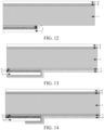
- FIG. 12 is a schematic diagram of a partial structure of an eighth type of back-contact solar cell according to an embodiment of the present invention.
- FIG. 13 is a schematic diagram of a partial structure of a ninth type of back-contact solar cell according to an embodiment of the present invention.
- FIG. 14 is a schematic diagram of a partial structure of a tenth type of back-contact solar cell according to an embodiment of the present invention.
- FIG. 11 is a schematic diagram of a partial structure of a seventh type of back-contact solar cell according to an embodiment of the present invention.
- FIG. 12 is a schematic diagram of a partial structure of an eighth type of back-contact solar cell according to an embodiment of the present invention.
- FIG. 13 is a schematic diagram of
- FIG. 15 is a schematic diagram of a partial structure of an eleventh type of back-contact solar cell according to an embodiment of the present invention.
- FIG. 16 is a schematic diagram of a partial structure of a twelfth type of back-contact solar cell according to an embodiment of the present invention.
- the method may further include a step of preparing a solar-cell body. Specifically, first, a textured structure is formed on a light receiving surface of a silicon substrate 1 through chemical etching, and a back surface of the silicon substrate 1 is etched and polished by using an alkaline or acidic solution. As shown in FIG. 10 , after the surface of the silicon substrate 1 is washed, a first passivation layer 7 and a first semiconductor layer 2 are deposited on a polished surface of the back surface of the silicon substrate 1, and an amorphous silicon passivation layer 8 and a silicon nitride (SiN x ) anti-reflection layer 9 are deposited on a texture of the light receiving surface of the silicon substrate 1. As shown in FIG.
- a blocking layer 3 with a height of 100 nm to 500 nm is deposited on the back surface of the structure shown in FIG. 10 by using a low-temperature CVD (Chemical Vapor Deposition, chemical vapor deposition) process.
- the blocking layer 3, the first semiconductor layer 2, and the first passivation layer 7 at a position opposite to a second region are removed by using a laser etching technology. Alternatively, the position opposite to the second region may be exposed through mask exposure.
- the blocking layer 3 is removed by using an HF (hydrofluoric acid) solution
- the first semiconductor layer 2 and the first passivation layer 7 are removed by using an alkaline solution
- a mask material is removed after patterning is completed.
- the first passivation layer 7 and a second semiconductor layer 4 are deposited in the second region of the back surface of the silicon substrate 1 and on the back surface of the blocking layer 3.
- the second semiconductor layer 4 and the first passivation layer 7 in a part of areas of the back surface of the blocking layer are removed by using the laser etching technology. Alternatively, the part of the areas of the back surface of the blocking layer are exposed through mask exposure. Then, the second semiconductor layer 4 and the first passivation layer 7 are removed by using an alkaline solution, and a material of a mask layer is removed after patterning is completed. As shown in FIG.
- an end of the blocking layer 3 away from the second semiconductor layer 4 is removed by using a hydrofluoric acid solution.
- a transparent conductive film layer is deposited on the entire back surface shown in FIG. 15 , and the solar-cell body is formed so far.
- the first electrode 11 and the second electrode 12 may be formed through electroplating. This is not specifically limited in the embodiments of the present invention.
- the methods in the embodiments may be implemented by using software plus a necessary universal hardware platform, and certainly may alternatively be implemented by hardware. However, in many cases, the former is a better implementation.
- the technical solutions of the present invention essentially or a part contributing to the prior art may be implemented in a form of a software product.
- the computer software product is stored in a storage medium (such as a ROM/RAM, a magnetic disk, or an optical disc), and includes several instructions to enable a terminal (which may be a mobile phone, a computer, a server, an air conditioner, a network device, or the like) to perform the methods in the embodiments of the present invention.
Landscapes
- Photovoltaic Devices (AREA)
Abstract
Description
- This application claims priority to
Chinese Patent Application No. 202210052750.8, entitled "BACK-CONTACT SOLAR CELL, MANUFACTURING METHOD THEREFOR, AND SOLAR-CELL ASSEMBLY", and filed with the China National Intellectual Property Administration on January 17, 2022 - The present invention relates to the field of solar-cell technologies, and in particular, to a back-contact solar cell, a manufacturing method therefor, and a solar-cell assembly.
- Back-contact solar cells have a wide application prospect due to a high open-circuit voltage and a high short-circuit current.
- In an existing back-contact solar cell, semiconductor layers of different doping types are arranged immediately adjacent to each other, and consequently, a short circuit easily occurs in the cell.
- The present disclosure provides a back-contact solar cell, a manufacturing method therefor, and a solar-cell assembly, to resolve a problem of a short circuit in an existing back-contact solar cell.
- According to a first aspect of the present invention, a back-contact solar cell is provided, including:
a solar-cell body, where the solar-cell body includes a silicon substrate, a first semiconductor layer located in a first region of a back surface of the silicon substrate, a blocking layer stacked on an end region of the first semiconductor layer, a second semiconductor layer stacked on the blocking layer and a second region of the back surface of the silicon substrate, and a transparent conductive film layer stacked on the first semiconductor layer and the second semiconductor layer. The first region and the second region are arranged immediately adjacent to each other. A doping type of the first semiconductor layer is different from a doping type of the second semiconductor layer. - A separation groove is provided on the second semiconductor layer and the transparent conductive film layer. An area of a cross section of the separation groove decreases toward the silicon substrate. A cross section of the separation groove is parallel to the silicon substrate.
- In this embodiment of the present invention, the separation groove is provided on the second semiconductor layer and the transparent conductive film layer, to physically separate the first semiconductor layer and the second semiconductor layer with different doping types, so that the back-contact solar cell has a better insulation effect, and a problem of a short circuit is avoided. The cross section of the separation groove is parallel to the silicon substrate, and the area of the cross section of the separation groove decreases toward the silicon substrate, so that light incident from a light receiving surface of the silicon substrate can be incident at each position of the separation groove, and the light incident at each position of the separation groove is reflected and reaches the silicon substrate. Therefore, an intensity of the light incident at the silicon substrate is higher, so that power of electricity generated by the back-contact solar cell is increased, photoelectric conversion efficiency of the back-contact solar cell is improved, and an open-circuit voltage and a short-circuit current of the back-contact solar cell are further increased.
- Optionally, a width of the cross section of the separation groove decreases toward the silicon substrate, and a direction of the width of the cross section of the separation groove is parallel to a direction along which the first region and the second region are arranged.
- Optionally, a refractive index of the transparent conductive film layer and a refractive index of the second semiconductor layer are both greater than a refractive index of the blocking layer.
- Optionally, the separation groove is filled with an insulating material.
- Optionally, the insulating material is light-permeable. The insulating material protrudes from the separation groove in a direction away from the silicon substrate. The insulating material protruding from the separation groove forms a hat-like structure. The hat-like structure includes a brim part and a crown part. An area of any cross section of the brim part is greater than an area of any cross section of the crown part. The brim part is closer to the separation groove. The area of each cross section of the brim part increases toward the silicon substrate. An area of a cross section of an end of the brim part close to the silicon substrate is greater than or equal to an area of a cross section of an end of the separation groove away from the silicon substrate. The cross sections are all parallel to the silicon substrate.
- Optionally, a width of any cross section of the brim part is greater than a width of any cross section of the crown part.
- The width of each cross section of the brim part increases toward the silicon substrate.
- A width of a cross section of an end of the brim part close to the separation groove is greater than or equal to a width of the cross section of the end of the separation groove away from the silicon substrate.
- A direction of the width of the cross section of the brim part is parallel to a direction along which the first region and the second region are arranged.
- Optionally, a refractive index of the insulating material is less than a refractive index of the blocking layer. The refractive index of the blocking layer is less than both a refractive index of the transparent conductive film layer and a refractive index of the second semiconductor layer.
- Optionally, the refractive index of the insulating material ranges from 0.05 to 1.7, the refractive index of the transparent conductive film layer ranges from 1.86 to 4.9, the refractive index of the second semiconductor layer ranges from 1.86 to 4.9, and the refractive index of the blocking layer ranges from 1.85 to 2.1.
- Optionally, the separation groove includes a first groove portion on the second semiconductor layer and a second groove portion on the transparent conductive film layer.
- A groove wall of the first groove portion includes a planar surface and/or a curvilinear surface;
and/or
a groove wall of the second groove portion includes a planar surface and/or a curvilinear surface. - Optionally, the groove wall of the first groove portion is a planar surface, the groove wall of the second groove portion is a planar surface, and the groove wall of the first groove portion and the groove wall of the second groove portion are distributed in a step shape, or the groove wall of the first groove portion forms a smooth transition with the groove wall of the second groove portion.
- Alternatively, the groove wall of the first groove portion is a curvilinear surface, the groove wall of the second groove portion is a curvilinear surface, and the curvilinear surface of the groove wall of the first groove portion and the curvilinear surface of the groove wall of the second groove portion have a same curvature.
- Optionally, the insulating material exactly fits a groove wall of the separation groove.
- Optionally, the insulating material includes an insulating ink and/or an insulating resin.
- Optionally, the solar-cell body further includes a back surface on the blocking layer and a first passivation layer in the second region of the back surface of the silicon substrate. The first passivation layer is located between the second semiconductor layer and the silicon substrate. A refractive index of the first passivation layer is greater than the refractive index of the blocking layer.
- The separation groove is formed through the first passivation layer, the second semiconductor layer, and the transparent conductive film layer.
- Optionally, a width of a cross section of an end of the separation groove close to the silicon substrate ranges from 10 µm to 80 µm, and the width of the cross section of the end of the separation groove away from the silicon substrate ranges from 20 µm to 90 µm.
- A width of a cross section of an end of the brim part close to the silicon substrate ranges from 30 µm to 120 µm.
- A width of a cross section of an end of the brim part away from the silicon substrate ranges from 20 µm to 110 µm.
- The cross section of the end of the separation groove close to the silicon substrate is parallel to the silicon substrate.
- A direction of the width of the cross section of the end of the separation groove close to the silicon substrate is parallel to the direction along which the first region and the second region are arranged.
- Optionally, the back-contact solar cell further includes a first electrode and a second electrode.
- The first electrode is located in a region of the transparent conductive film layer opposite to the first semiconductor layer.
- The second electrode is located in a region of the transparent conductive film layer opposite to the second semiconductor layer.
- The hat-like structure is located between the first electrode and the second electrode, and an end of the hat-like structure away from the silicon substrate protrudes out of the first electrode and the second electrode.
- Optionally, a height by which the hat-like structure protrudes out of the first electrode ranges from 0.1 µm to 50 µm.
- A direction of the height is parallel to a stacking direction of the first semiconductor layer and the silicon substrate.
- Optionally, a height of the blocking layer ranges from 100 nm to 500 nm, and a direction of the height is parallel to a stacking direction of the first semiconductor layer and the silicon substrate.
- Optionally, the first region does not overlap the second region.
- Optionally, the silicon substrate is an N-type silicon substrate, the first semiconductor layer is a P-type doped microcrystalline silicon layer, the second semiconductor layer is an N+ doped amorphous silicon layer, the blocking layer is a silicon nitride blocking layer, and the first passivation layer is an amorphous silicon layer.
- Optionally, the first passivation layer is further distributed in the first region of the back surface of the silicon substrate, and the first passivation layer is located between the first semiconductor layer and the silicon substrate.
- Optionally, the back-contact solar cell further includes an amorphous silicon passivation layer on a light receiving surface of the silicon substrate, and a silicon nitride anti-reflection layer on a light receiving surface of the amorphous silicon passivation layer; and/or
the light receiving surface of the silicon substrate has a textured structure. - According to a second aspect of the present invention, a method for manufacturing a back-contact solar cell is further provided. The method is for manufacturing any one of the back-contact solar cells described above.
- Optionally, the separation groove is formed on the second semiconductor layer and the transparent conductive film layer by using a Gaussian beam.
- Optionally, a wavelength of the Gaussian beam ranges from 900 nm to 1200 nm, and an energy density of the Gaussian beam ranges from 0.1 J/cm2 to 0.5 J/cm2.
- Optionally, the method further includes: printing an insulating material in the separation groove.
- According to a third aspect of the present invention, a solar-cell assembly is further provided, including any one of the back-contact solar cells described above.
- The foregoing descriptions are merely an overview of the technical solutions of the present invention. To understand the technical means of the present invention more clearly, the technical means of the present invention may be implemented according to content of this specification. In addition, to make the foregoing and other objectives, features, and advantages of the present invention clearer and more comprehensible, specific implementations of the present invention are described below.
- To describe the technical solutions in embodiments of the present invention more clearly, the accompanying drawings required for describing the embodiments of the present invention are briefly described below. It is clear that the accompanying drawings in the following descriptions are merely some embodiments of the present invention, and a person of ordinary skill in the art may further derive other drawings based on the accompanying drawings without creative efforts.
-
FIG. 1 is a schematic diagram of a partial structure of a first type of back-contact solar cell according to an embodiment of the present invention; -
FIG. 2 is a schematic diagram of a part of light paths in a back-contact solar cell according to an embodiment of the present invention; -
FIG. 3 is a schematic diagram of a partial structure of a second type of back-contact solar cell according to an embodiment of the present invention; -
FIG. 4 is a schematic diagram of a part of light paths in an insulating material in a back-contact solar cell according to an embodiment of the present invention; -
FIG. 5 is a schematic diagram of a partial structure of a third type of back-contact solar cell according to an embodiment of the present invention; -
FIG. 6 is a schematic diagram of a partial structure of a fourth type of back-contact solar cell according to an embodiment of the present invention; -
FIG. 7 is a schematic diagram of a partial structure of a fifth type of back-contact solar cell according to an embodiment of the present invention; -
FIG. 8 is a schematic diagram of a structure of a back-contact solar cell according to an embodiment of the present invention; -
FIG. 9 is a schematic diagram of energy distribution of a Gaussian beam for grooving according to an embodiment of the present invention; -
FIG. 10 is a schematic diagram of a partial structure of a sixth type of back-contact solar cell according to an embodiment of the present invention; -
FIG. 11 is a schematic diagram of a partial structure of a seventh type of back-contact solar cell according to an embodiment of the present invention; -
FIG. 12 is a schematic diagram of a partial structure of an eighth type of back-contact solar cell according to an embodiment of the present invention; -
FIG. 13 is a schematic diagram of a partial structure of a ninth type of back-contact solar cell according to an embodiment of the present invention; -
FIG. 14 is a schematic diagram of a partial structure of a tenth type of back-contact solar cell according to an embodiment of the present invention; -
FIG. 15 is a schematic diagram of a partial structure of an eleventh type of back-contact solar cell according to an embodiment of the present invention; and -
FIG. 16 is a schematic diagram of a partial structure of a twelfth type of back-contact solar cell according to an embodiment of the present invention. - 1-silicon substrate, 2-first semiconductor layer, 3-blocking layer, 4-second semiconductor layer, 5-transparent conductive film layer, 6-separation groove, 61-groove wall of a first groove portion, 62-groove wall of a second groove portion, 7-first passivation layer, 8-amorphous silicon passivation layer, 9-silicon nitride anti-reflection layer, 10-insulating material, 101-hat-like structure, 1011-brim part, 1012-crown part, 11-first electrode, and 12-second electrode.
- The technical solutions in embodiments of the present invention are clearly and completely described below with reference to the accompanying drawings of the embodiments of the present invention. It is clear that the described embodiments are a part of the embodiments of the present invention, rather than all of the embodiments. Based on the embodiments of the present invention, all other embodiments obtained by a person of ordinary skill in the art without creative efforts shall fall within the protection scope of the present invention.
- A back-contact solar cell may be an IBC solar cell (interdigitated back-contact solar cell), an HBC solar cell (heterojunction interdigitated back-contact solar cell), or the like. This is not specifically limited in the embodiments of the present invention.
FIG. 1 is a schematic diagram of a partial structure of a first type of back-contact solar cell according to an embodiment of the present invention. As shown inFIG. 1 , the back-contact solar cell includes a solar-cell body. The solar-cell body includes asilicon substrate 1. A doping type of thesilicon substrate 1 is not specifically limited. A light receiving surface of thesilicon substrate 1 is a surface of thesilicon substrate 1 in the back-contact solar cell that receives light. A back surface of thesilicon substrate 1 is a surface of thesilicon substrate 1 that is opposite to the light receiving surface. The solar-cell body further includes afirst semiconductor layer 2 located in a first region of the back surface of thesilicon substrate 1, ablocking layer 3 stacked on an end region of thefirst semiconductor layer 2, asecond semiconductor layer 4 stacked on theblocking layer 3 and a second region of the back surface of thesilicon substrate 1, and a transparentconductive film layer 5 stacked on thefirst semiconductor layer 2 and thesecond semiconductor layer 4. The end region of thefirst semiconductor layer 2 may be an area that is on thefirst semiconductor layer 2 and that is close to an end of thesecond semiconductor layer 4. A relative size of the end region relative to thefirst semiconductor layer 2 is not specifically limited. The first region and the second region are arranged immediately adjacent to each other, and the relative size of the first region relative to the second region is not specifically limited. A doping type of thefirst semiconductor layer 2 is different from a doping type of thesecond semiconductor layer 4. One of thefirst semiconductor layer 2 and thesecond semiconductor layer 4 is P-type doped, and the other is N-type doped. - A
separation groove 6 is provided on thesecond semiconductor layer 4 and the transparentconductive film layer 5. Theseparation groove 6 physically separates thefirst semiconductor layer 2 and thesecond semiconductor layer 4 with different doping types, so that the back-contact solar cell has a better insulation effect. - A direction shown by a dashed-line arrow L in
FIG. 1 is a direction toward thesilicon substrate 1. An area of a cross section of theseparation groove 6 decreases toward thesilicon substrate 1, and the cross section of theseparation groove 6 is parallel to thesilicon substrate 1. Cross sections described below are all parallel to thesilicon substrate 1.FIG. 2 is a schematic diagram of a part of light paths in a back-contact solar cell according to an embodiment of the present invention. A thicker arrow inFIG. 2 shows light. As shown inFIG. 2 , the cross section of theseparation groove 6 is parallel to thesilicon substrate 1, and the area of the cross section of theseparation groove 6 decreases toward thesilicon substrate 1, so that light incident from the light receiving surface of thesilicon substrate 1 can be incident at each position of theseparation groove 6, and the light incident at each position of theseparation groove 6 is reflected and reaches thesilicon substrate 1. Therefore, an intensity of the light incident at thesilicon substrate 1 is higher, so that power of electricity generated by the back-contact solar cell is increased, photoelectric conversion efficiency of the back-contact solar cell is improved, and an open-circuit voltage and a short-circuit current of the back-contact solar cell are further increased. - Optionally, as shown in
FIG. 1 , a width of the cross section of theseparation groove 6 decreases toward thesilicon substrate 1, and a direction of the width of the cross section of theseparation groove 6 is parallel to a direction along which the first region and the second region of the back surface of thesilicon substrate 1 are arranged. Therefore, the light incident from the light receiving surface of thesilicon substrate 1 can further be incident at each position of theseparation groove 6, and the light incident at each position of theseparation groove 6 is reflected and reaches thesilicon substrate 1, so that the intensity of the light incident at thesilicon substrate 1 is higher. For example, a width of a cross section of an end of theseparation groove 6 close to thesilicon substrate 1 is w1, and a width of a cross section of an end of theseparation groove 6 away from thesilicon substrate 1 is w2. In this case, w2 > w1. It needs to be noted that widths mentioned below are all parallel to the direction along which the first region and the second region of the back surface of thesilicon substrate 1 are arranged. - Optionally, a refractive index of the transparent
conductive film layer 5 and a refractive index of thesecond semiconductor layer 4 are both greater than a refractive index of theblocking layer 3. Therefore, less light incident from the light receiving surface of thesilicon substrate 1 is refracted to the outside of the back-contact solar cell, and more light is incident at each position of theseparation groove 6, so that the intensity of the light incident at thesilicon substrate 1 is further improved. -
FIG. 3 is a schematic diagram of a partial structure of a second type of back-contact solar cell according to an embodiment of the present invention. Optionally, theseparation groove 6 is filled with an insulatingmaterial 10. On the basis that theseparation groove 6 is physically insulated, electrical insulation is further performed by using the insulatingmaterial 10, so that an insulation effect is optimized, and a fill factor of the back-contact solar cell is improved. In addition, the insulatingmaterial 10 can further reflect received light onto thesilicon substrate 1, so that the intensity of the light incident at thesilicon substrate 1 is higher. It needs to be noted that the insulatingmaterial 10 may be a thermosetting insulating material. The insulatingmaterial 10 may further have a strong acid-resistance characteristic or a strong alkali-resistance characteristic, so that the insulatingmaterial 10 has good stability during subsequent processing and use. - Optionally, the insulating
material 10 includes an insulating ink and/or an insulating resin. A good insulation effect is achieved, and costs are low. - Optionally, the insulating
material 10 is light-permeable, and the light received from the light receiving surface of thesilicon substrate 1 can be transmitted into the insulatingmaterial 10. Strength of light permeability of the insulatingmaterial 10 is not specifically limited. The insulatingmaterial 10 protrudes from theseparation groove 6 in a direction away from thesilicon substrate 1. The insulatingmaterial 10 protruding from theseparation groove 6 forms a hat-like structure 101. The hat-like structure 101 includes abrim part 1011 and acrown part 1012. An area of any cross section of thebrim part 1011 is greater than an area of any cross section of thecrown part 1012. Thebrim part 1011 is closer to theseparation groove 6 than thecrown part 1012. The area of each cross section of thebrim part 1011 increases toward thesilicon substrate 1, in other words, in the direction shown by the dashed-line arrow L in the figure. An area of a cross section of an end of thebrim part 1011 close to theseparation groove 6 is greater than or equal to an area of a cross section of an end of theseparation groove 6 away from thesilicon substrate 1. The foregoing cross sections are all parallel to thesilicon substrate 1. -
FIG. 4 is a schematic diagram of a part of light paths in an insulating material in a back-contact solar cell according to an embodiment of the present invention. A thicker arrow inFIG. 4 shows light. As shown inFIG. 4 , if the light incident from the light receiving surface of thesilicon substrate 1 is incident at theseparation groove 6, the light is reflected by theseparation groove 6 and reaches the transparentconductive film layer 5, and is reflected by the transparentconductive film layer 5 and reaches thesilicon substrate 1. If the light is incident at thebrim part 1011, the light may be reflected by thebrim part 1011 and reaches thecrown part 1012, then the light is reflected by thecrown part 1012 and incident at thebrim part 1011 again, and the light is reflected and reaches thesilicon substrate 1. If the light is incident at thecrown part 1012, the light may be reflected by thecrown part 1012 and incident at thebrim part 1011 again, and then the light is reflected and reaches thesilicon substrate 1. Therefore, the intensity of the light incident at thesilicon substrate 1 is higher, so that the power of the electricity generated by the back-contact solar cell is increased, the photoelectric conversion efficiency of the back-contact solar cell is improved, and the open-circuit voltage and the short-circuit current of the back-contact solar cell are further increased. - Optionally, as shown in
FIG. 3 , a width of any cross section of thebrim part 1011 is greater than a width of any cross section of thecrown part 1012, so that the insulatingmaterial 10 can receive incident light of a large range. - The width of each cross section of the
brim part 1011 increases toward thesilicon substrate 1, in other words, in the direction shown by the dashed-line arrow L in the figure. Parts of thebrim part 1011 are not blocked by each other, and all can receive light. For example, inFIG. 4 , a width of a cross section of an end of thebrim part 1011 away from thesilicon substrate 1 is w4, and a width of a cross section of an end of thebrim part 1011 close to thesilicon substrate 1 is w3, where w3 > w4. - w3 represents the width of the cross section of the end of the
brim part 1011 close to thesilicon substrate 1, i.e., a width of a cross section of an end of thebrim part 1011 close to theseparation groove 6. The width of the cross section of the end of theseparation groove 6 away from thesilicon substrate 1 is w2, where w3 ≥ w2. After an electrode is subsequently disposed, thebrim part 1011 of the foregoing structure can prevent the electrode from contacting thesecond semiconductor layer 4, to avoid an adverse effect of the electrode on thesecond semiconductor layer 4. - A direction of the width of the cross section of the
brim part 1011 is parallel to a direction along which the first region and the second region are arranged. - Optionally, a refractive index of the insulating
material 10 is less than a refractive index of theblocking layer 3, and the refractive index of theblocking layer 3 is less than both a refractive index of the transparentconductive film layer 5 and a refractive index of thesecond semiconductor layer 4. Therefore, less light is refracted out of the back-contact solar cell, and more light is reflected by theseparation groove 6 and the insulatingmaterial 10 and reaches thesilicon substrate 1, to further improve the intensity of the light incident at thesilicon substrate 1. - Optionally, the refractive index of the insulating
material 10 ranges from 0.05 to 1.7, the refractive index of the transparentconductive film layer 5 ranges from 1.86 to 4.9, the refractive index of thesecond semiconductor layer 4 ranges from 1.86 to 4.9, and the refractive index of theblocking layer 3 ranges from 1.85 to 2.1. In the foregoing distribution manner of the refractive indexes, the refractive indexes of the structures match well, so that the light refracted out of the back-contact solar cell can be further reduced, and the light that is reflected by theseparation groove 6 and the insulatingmaterial 10 and reaches thesilicon substrate 1 is further increased. - Optionally, the
separation groove 6 includes a first groove portion on thesecond semiconductor layer 4 and a second groove portion on the transparentconductive film layer 5. A groove wall of the first groove portion includes a planar surface and/or a curvilinear surface. In other words, the groove walls of the first groove portion on thesecond semiconductor layer 4 may all be planar surfaces or curvilinear surfaces, or may be a combination of a planar surface and a curvilinear surface. The first groove portion has various forms. In addition/Alternatively, a groove wall of the second groove portion includes a planar surface and/or a curvilinear surface. In other words, the groove walls of the second groove portion on the transparentconductive film layer 5 may all be planar surfaces or curvilinear surfaces, or may be a combination of a planar surface and a curvilinear surface. The second groove portion has various forms. -
FIG. 5 is a schematic diagram of a partial structure of a third type of back-contact solar cell according to an embodiment of the present invention.FIG. 6 is a schematic diagram of a partial structure of a fourth type of back-contact solar cell according to an embodiment of the present invention.FIG. 7 is a schematic diagram of a partial structure of a fifth type of back-contact solar cell according to an embodiment of the present invention. For example, as shown inFIG. 5 and FIG. 6 , thegroove walls 61 of the first groove portion are all planar surfaces, and thegroove walls 62 of the second groove portion are all planar surfaces. InFIG. 7 , thegroove walls 61 of the first groove portion are all curvilinear surfaces, and thegroove walls 62 of the second groove portion are all curvilinear surfaces. - Optionally, as shown in
FIG. 5 and FIG. 6 , thegroove wall 61 of the first groove portion is a planar surface, and thegroove wall 62 of the second groove portion is a planar surface. InFIG. 5 , thegroove wall 61 of the first groove portion and thegroove wall 62 of the second groove portion are distributed in a step shape. Alternatively, inFIG. 6 , thegroove wall 61 of the first groove portion forms a smooth transition with thegroove wall 62 of the second groove portion, and the planar surface of thegroove wall 61 of the first groove portion and the planar surface of thegroove wall 62 of the second groove portion have a same slope. Theseparation groove 6 has various forms. - Optionally, as shown in
FIG. 7 , thegroove wall 61 of the first groove portion is a curvilinear surface, and thegroove wall 62 of the second groove portion is a curvilinear surface. The curvilinear surface of thegroove wall 61 of the first groove portion and the curvilinear surface of thegroove wall 62 of the second groove portion have a same curvature. Thegroove wall 61 of the first groove portion and thegroove wall 62 of the second groove portion may be on a same circle, so that it is convenient to process theseparation groove 6. - Optionally, as shown in
FIG. 3 and FIG. 4 , the insulatingmaterial 10 exactly fits a groove wall of theseparation groove 6. Therefore, the subsequent electrode does not enter between the insulatingmaterial 10 and theseparation groove 6, so that not only a waste of an electrode material can be reduced, but also a short circuit can be effectively prevented. - Optionally, referring to
FIG. 1 to FIG. 7 , the solar-cell body further includes a back surface on theblocking layer 3 and afirst passivation layer 7 in the second region of the back surface of thesilicon substrate 1. Thefirst passivation layer 7 is located between thesecond semiconductor layer 4 and thesilicon substrate 1. A refractive index of thefirst passivation layer 7 is greater than the refractive index of theblocking layer 3. Therefore, a passivation function is good, and less light is refracted out of the back-contact solar cell. - The
separation groove 6 is formed through thefirst passivation layer 7, thesecond semiconductor layer 4, and the transparentconductive film layer 5. A shape or the like of a groove wall of a groove portion of theseparation groove 6 on thefirst passivation layer 7 is not specifically limited. - Optionally, as shown in
FIG. 1 andFIG. 3 , the width w1 of the cross section of the end of theseparation groove 6 close to thesilicon substrate 1 ranges from 10 µm (micrometer) to 80 µm, and the width w2 of the cross section of the end of theseparation groove 6 away from thesilicon substrate 1 ranges from 20 µm to 90 µm. Alight reflection effect and an insulation effect of theseparation groove 6 of the foregoing size are both good. - Optionally, as shown in
FIG. 3 , the width w3 of the cross section of the end of thebrim part 1011 close to thesilicon substrate 1 ranges from 30 µm to 120 µm, and the width w4 of the cross section of the end of thebrim part 1011 away from thesilicon substrate 1 ranges from 20 µm to 110 µm. A light reflection effect and an insulation effect of thebrim part 1011 of the foregoing size are both good. -
FIG. 8 is a schematic diagram of a structure of a back-contact solar cell according to an embodiment of the present invention. As shown inFIG. 8 , the back-contact solar cell further includes afirst electrode 11 and asecond electrode 12. Thefirst electrode 11 is located in a region of the transparentconductive film layer 5 opposite to thefirst semiconductor layer 2. Thesecond electrode 12 is located in a region of the transparentconductive film layer 5 opposite to thesecond semiconductor layer 4. - Optionally, as shown in
FIG. 8 , the hat-like structure 101 is located between thefirst electrode 11 and thesecond electrode 12, and an end of the hat-like structure 101 away from thesilicon substrate 1 protrudes out of thefirst electrode 11 and thesecond electrode 12. The hat-like structure 101 protrudes out of thefirst electrode 11 and thesecond electrode 12, so that a short circuit between thefirst electrode 11 and thesecond electrode 12 can be sufficiently prevented. Specifically, whether both the brim part and the crown part include a part that protrudes out of thefirst electrode 11 or only the crown part includes a part that protrudes out of the first electrode is not specifically limited. - Optionally, as shown in
FIG. 8 , a height h1 by which the hat-like structure 101 protrudes out of thefirst electrode 11 ranges from 0.1 µm to 50 µm. The height range can not only well prevent a short circuit between thefirst electrode 11 and thesecond electrode 12, but also prevent the protruding part from causing a large stress during formation of a solar-cell assembly. A direction of the height h1 by which the hat-like structure 101 protrudes out of thefirst electrode 11 is parallel to a stacking direction of thefirst semiconductor layer 2 and thesilicon substrate 1. Directions of heights mentioned below are all parallel to the stacking direction of thefirst semiconductor layer 2 and thesilicon substrate 1. - Optionally, as shown in
FIG. 8 , a height h2 of theblocking layer 3 ranges from 100 nm to 500 nm. The blocking layer provides a good separation effect when its height falls within this range. - Optionally, referring to
FIG. 1 to FIG. 4 , andFIG. 8 , the first region does not overlap the second region, so that a good insulation effect is achieved. - Optionally, the
silicon substrate 1 is an N-type silicon substrate, thefirst semiconductor layer 2 is a P-type doped microcrystalline silicon layer, thesecond semiconductor layer 4 is an N+ doped amorphous silicon layer, theblocking layer 3 is a silicon nitride blocking layer, and thefirst passivation layer 7 is an amorphous silicon layer. - Optionally, referring to
FIG. 1 to FIG. 4 , andFIG. 8 , thefirst passivation layer 7 is further distributed in the first region of the back surface of thesilicon substrate 1, and thefirst passivation layer 7 is located between thefirst semiconductor layer 2 and thesilicon substrate 1, so that a good passivation effect is achieved. - Optionally, as shown in
FIG. 1 to FIG. 3 , andFIG. 8 , the back-contact solar cell further includes an amorphoussilicon passivation layer 8 on the light receiving surface of thesilicon substrate 1, and a silicon nitride (SiNx)anti-reflection layer 9 on a light receiving surface of the amorphoussilicon passivation layer 8. A value of x is not specifically limited. The amorphoussilicon passivation layer 8 may be an intrinsic amorphous silicon layer. - Optionally, the light receiving surface of the
silicon substrate 1 has a textured structure, to further extend an optical path of light in the back-contact solar cell. - The present invention further provides a solar-cell assembly, including any one of the back-contact solar cells described above. The solar-cell assembly has a beneficial effect the same as or similar to those of the back-contact solar cells described above. To avoid repetition, details are not described herein again.
- An embodiment of the present invention further provides a method for manufacturing a back-contact solar cell. The method is for manufacturing any one of the back-contact solar cells described above. The method for manufacturing a back-contact solar cell has a beneficial effect the same as or similar to those of the back-contact solar cells described above.
- Optionally, the method for manufacturing a back-contact solar cell may further include the following step: forming the
separation groove 6 on thesecond semiconductor layer 4 and the transparentconductive film layer 5 by using a Gaussian beam. The foregoing grooving method is simple, and an adverse effect such as pollution on a solar-cell body is small. For example, theseparation groove 6 is provided by using a Gaussian spot laser. -
FIG. 9 is a schematic diagram of energy distribution of a Gaussian beam for grooving according to an embodiment of the present invention. It can be seen fromFIG. 9 that, energy of a laser spot is conically distributed. The energy is high in a center and gradually decreases in a peripheral direction. As shown inFIG. 9 , optionally, a wavelength of the Gaussian beam ranges from 900 nm (nanometer) to 1200 nm, and an energy density of the Gaussian beam ranges from 0.1 J/cm2 (joules per square centimeter) to 0.5 J/cm2. The separation groove is provided at a faster speed by using the Gaussian beam. - Optionally, the method may further include: printing an insulating
material 10 in theseparation groove 6. A manner of disposing the insulatingmaterial 10 is simple. -
FIG. 10 is a schematic diagram of a partial structure of a sixth type of back-contact solar cell according to an embodiment of the present invention.FIG. 11 is a schematic diagram of a partial structure of a seventh type of back-contact solar cell according to an embodiment of the present invention.FIG. 12 is a schematic diagram of a partial structure of an eighth type of back-contact solar cell according to an embodiment of the present invention.FIG. 13 is a schematic diagram of a partial structure of a ninth type of back-contact solar cell according to an embodiment of the present invention.FIG. 14 is a schematic diagram of a partial structure of a tenth type of back-contact solar cell according to an embodiment of the present invention.FIG. 15 is a schematic diagram of a partial structure of an eleventh type of back-contact solar cell according to an embodiment of the present invention.FIG. 16 is a schematic diagram of a partial structure of a twelfth type of back-contact solar cell according to an embodiment of the present invention. - The method may further include a step of preparing a solar-cell body. Specifically, first, a textured structure is formed on a light receiving surface of a
silicon substrate 1 through chemical etching, and a back surface of thesilicon substrate 1 is etched and polished by using an alkaline or acidic solution. As shown inFIG. 10 , after the surface of thesilicon substrate 1 is washed, afirst passivation layer 7 and afirst semiconductor layer 2 are deposited on a polished surface of the back surface of thesilicon substrate 1, and an amorphoussilicon passivation layer 8 and a silicon nitride (SiNx)anti-reflection layer 9 are deposited on a texture of the light receiving surface of thesilicon substrate 1. As shown inFIG. 11 , ablocking layer 3 with a height of 100 nm to 500 nm is deposited on the back surface of the structure shown inFIG. 10 by using a low-temperature CVD (Chemical Vapor Deposition, chemical vapor deposition) process. As shown inFIG. 12 , theblocking layer 3, thefirst semiconductor layer 2, and thefirst passivation layer 7 at a position opposite to a second region are removed by using a laser etching technology. Alternatively, the position opposite to the second region may be exposed through mask exposure. Then, theblocking layer 3 is removed by using an HF (hydrofluoric acid) solution, thefirst semiconductor layer 2 and thefirst passivation layer 7 are removed by using an alkaline solution, and a mask material is removed after patterning is completed. As shown inFIG. 13 , thefirst passivation layer 7 and asecond semiconductor layer 4 are deposited in the second region of the back surface of thesilicon substrate 1 and on the back surface of theblocking layer 3. As shown inFIG. 14 , thesecond semiconductor layer 4 and thefirst passivation layer 7 in a part of areas of the back surface of the blocking layer are removed by using the laser etching technology. Alternatively, the part of the areas of the back surface of the blocking layer are exposed through mask exposure. Then, thesecond semiconductor layer 4 and thefirst passivation layer 7 are removed by using an alkaline solution, and a material of a mask layer is removed after patterning is completed. As shown inFIG. 15 , an end of theblocking layer 3 away from thesecond semiconductor layer 4 is removed by using a hydrofluoric acid solution. As shown inFIG. 16 , a transparent conductive film layer is deposited on the entire back surface shown inFIG. 15 , and the solar-cell body is formed so far. - The
first electrode 11 and thesecond electrode 12 may be formed through electroplating. This is not specifically limited in the embodiments of the present invention. - The foregoing method for manufacturing a back-contact solar cell can achieve a beneficial effect the same as or similar to those of the back-contact solar cells described above. For related content of the two, reference can be made to each other. To avoid repetition, details are not described herein again.
- It needs to be noted that, for ease of description, the method embodiments are described as a series of action combinations. However, a person skilled in the art should know that the embodiments of this application are not limited to the described order of actions, because some steps may be performed in another order or simultaneously according to the embodiments of this application. In addition, a person skilled in the art should also learn that, the embodiments described in this specification are all preferred embodiments, and actions involved are not necessarily all required in the embodiments of this application.
- It needs to be noted that, in this specification, terms "include", "comprise", or any other variant thereof are intended to cover non-exclusive inclusion, so that a process, method, product, or apparatus that includes a series of elements includes not only the elements, but also another element not expressly listed, or an element inherent to such a process, method, product, or apparatus. An element defined by a statement "includes a... " does not exclude, without more limitations, existence of another same element in a process, method, product, or apparatus that includes the element.
- According to the foregoing descriptions of the implementations, a person skilled in the art may clearly understand that the methods in the embodiments may be implemented by using software plus a necessary universal hardware platform, and certainly may alternatively be implemented by hardware. However, in many cases, the former is a better implementation. Based on this understanding, the technical solutions of the present invention essentially or a part contributing to the prior art may be implemented in a form of a software product. The computer software product is stored in a storage medium (such as a ROM/RAM, a magnetic disk, or an optical disc), and includes several instructions to enable a terminal (which may be a mobile phone, a computer, a server, an air conditioner, a network device, or the like) to perform the methods in the embodiments of the present invention.
- The embodiments of the present invention are described above with reference to the accompanying drawings. However, the present invention is not limited to the foregoing specific implementations. The foregoing specific implementations are merely illustrative rather than restrictive. A person of ordinary skill in the art can make many forms in light of the present invention without departing from the spirit of the present invention and the protection scope of the claims. These forms all fall within the protection of the present invention.
Claims (26)
- A back-contact solar cell, comprising:a solar-cell body, wherein the solar-cell body comprises a silicon substrate, a first semiconductor layer located in a first region of a back surface of the silicon substrate, a blocking layer stacked on an end region of the first semiconductor layer, a second semiconductor layer stacked on the blocking layer and a second region of the back surface of the silicon substrate, and a transparent conductive film layer stacked on the first semiconductor layer and the second semiconductor layer; the first region and the second region are arranged immediately adjacent to each other; a doping type of the first semiconductor layer is different from a doping type of the second semiconductor layer; anda separation groove is provided on the second semiconductor layer and the transparent conductive film layer; an area of a cross section of the separation groove decreases toward the silicon substrate, and the cross section of the separation groove is parallel to the silicon substrate.
- The back-contact solar cell according to claim 1, wherein a width of the cross section of the separation groove decreases toward the silicon substrate; and a direction of the width of the cross section of the separation groove is parallel to a direction along which the first region and the second region are arranged.
- The back-contact solar cell according to claim 1, wherein a refractive index of the transparent conductive film layer and a refractive index of the second semiconductor layer are both greater than a refractive index of the blocking layer.
- The back-contact solar cell according to claim 1, wherein the separation groove is filled with an insulating material.
- The back-contact solar cell according to claim 4, wherein the insulating material is light-permeable, the insulating material protrudes from the separation groove in a direction away from the silicon substrate; the insulating material protruding from the separation groove forms a hat-like structure, the hat-like structure comprises a brim part and a crown part, and an area of any cross section of the brim part is greater than an area of any cross section of the crown part; the brim part is closer to the separation groove, the area of each cross section of the brim part increases toward the silicon substrate; an area of a cross section of an end of the brim part close to the silicon substrate is greater than or equal to an area of a cross section of an end of the separation groove away from the silicon substrate; and the cross sections are all parallel to the silicon substrate.
- The back-contact solar cell according to claim 5, wherein a width of any cross section of the brim part is greater than a width of any cross section of the crown part;the width of each cross section of the brim part increases toward the silicon substrate;a width of a cross section of an end of the brim part close to the separation groove is greater than or equal to a width of the cross section of the end of the separation groove away from the silicon substrate; anda direction of the width of the cross section of the brim part is parallel to a direction along which the first region and the second region are arranged.
- The back-contact solar cell according to claim 5, wherein a refractive index of the insulating material is less than a refractive index of the blocking layer, and the refractive index of the blocking layer is less than both a refractive index of the transparent conductive film layer and a refractive index of the second semiconductor layer.
- The back-contact solar cell according to claim 7, wherein the refractive index of the insulating material ranges from 0.05 to 1.7, the refractive index of the transparent conductive film layer ranges from 1.86 to 4.9, the refractive index of the second semiconductor layer ranges from 1.86 to 4.9, and the refractive index of the blocking layer ranges from 1.85 to 2.1.
- The back-contact solar cell according to any one of claims 1 to 8, wherein the separation groove comprises a first groove portion on the second semiconductor layer and a second groove portion on the transparent conductive film layer;a groove wall of the first groove portion comprises a planar surface and/or a curvilinear surface;
and/ora groove wall of the second groove portion comprises a planar surface and/or a curvilinear surface. - The back-contact solar cell according to claim 9, wherein the groove wall of the first groove portion is a planar surface, the groove wall of the second groove portion is a planar surface, and the groove wall of the first groove portion and the groove wall of the second groove portion are distributed in a step shape, or the groove wall of the first groove portion forms a smooth transition with the groove wall of the second groove portion; or
the groove wall of the first groove portion is a curvilinear surface, the groove wall of the second groove portion is a curvilinear surface, and the curvilinear surface of the groove wall of the first groove portion and the curvilinear surface of the groove wall of the second groove portion have a same curvature. - The back-contact solar cell according to any one of claims 4 to 8, wherein the insulating material exactly fits a groove wall of the separation groove.
- The back-contact solar cell according to any one of claims 4 to 8, wherein the insulating material comprises an insulating ink and/or an insulating resin.
- The back-contact solar cell according to any one of claims 1 to 8, wherein the solar-cell body further comprises a back surface on the blocking layer and a first passivation layer in the second region of the back surface of the silicon substrate, the first passivation layer is located between the second semiconductor layer and the silicon substrate; a refractive index of the first passivation layer is greater than the refractive index of the blocking layer; and
the separation groove is formed through the first passivation layer, the second semiconductor layer, and the transparent conductive film layer. - The back-contact solar cell according to claim 5 or 6, wherein a width of a cross section of an end of the separation groove close to the silicon substrate ranges from 10 µm to 80 µm, and the width of the cross section of the end of the separation groove away from the silicon substrate ranges from 20 µm to 90 µm;a width of a cross section of an end of the brim part close to the silicon substrate ranges from 30 µm to 120 µm;a width of a cross section of an end of the brim part away from the silicon substrate ranges from 20 µm to 110 µm;the cross section of the end of the separation groove close to the silicon substrate is parallel to the silicon substrate; anda direction of the width of the cross section of the end of the separation groove close to the silicon substrate is parallel to the direction along which the first region and the second region are arranged.
- The back-contact solar cell according to claim 5, further comprising a first electrode and a second electrode, whereinthe first electrode is located in a region of the transparent conductive film layer opposite to the first semiconductor layer;the second electrode is located in a region of the transparent conductive film layer opposite to the second semiconductor layer; andthe hat-like structure is located between the first electrode and the second electrode, and an end of the hat-like structure away from the silicon substrate protrudes out of the first electrode and the second electrode.
- The back-contact solar cell according to claim 15, wherein a height by which the hat-like structure protrudes out of the first electrode ranges from 0.1 µm to 50 µm; and
a direction of the height is parallel to a stacking direction of the first semiconductor layer and the silicon substrate. - The back-contact solar cell according to any one of claims 1 to 8, wherein a height of the blocking layer ranges from 100 nm to 500 nm, and a direction of the height is parallel to a stacking direction of the first semiconductor layer and the silicon substrate.
- The back-contact solar cell according to any one of claims 1 to 8, wherein the first region does not overlap the second region.
- The back-contact solar cell according to claim 13, wherein the silicon substrate is an N-type silicon substrate, the first semiconductor layer is a P-type doped microcrystalline silicon layer, the second semiconductor layer is an N+ doped amorphous silicon layer, the blocking layer is a silicon nitride blocking layer, and the first passivation layer is an amorphous silicon layer.
- The back-contact solar cell according to claim 13, wherein the first passivation layer is further distributed in the first region of the back surface of the silicon substrate, and the first passivation layer is located between the first semiconductor layer and the silicon substrate.
- The back-contact solar cell according to any one of claims 1 to 8, wherein the back-contact solar cell further comprises an amorphous silicon passivation layer on a light receiving surface of the silicon substrate, and a silicon nitride anti-reflection layer on a light receiving surface of the amorphous silicon passivation layer; and/or
the light receiving surface of the silicon substrate has a textured structure. - A method for manufacturing a back-contact solar cell, wherein the method is for manufacturing the back-contact solar cell according to any one of claims 1 to 21.
- The method for manufacturing a back-contact solar cell according to claim 22, wherein the method comprises:
forming the separation groove on the second semiconductor layer and the transparent conductive film layer by using a Gaussian beam. - The method for manufacturing a back-contact solar cell according to claim 23, wherein a wavelength of the Gaussian beam ranges from 900 nm to 1200 nm, and an energy density of the Gaussian beam ranges from 0.1 J/cm2 to 0.5 J/cm2.
- The method for manufacturing a back-contact solar cell according to any one of claims 22 to 24, wherein the method further comprises: printing an insulating material in the separation groove.
- A solar-cell assembly, comprising: the back-contact solar cell according to any one of claims 1 to 21.
Applications Claiming Priority (2)
| Application Number | Priority Date | Filing Date | Title |
|---|---|---|---|
| CN202210052750.8A CN116487450A (en) | 2022-01-17 | 2022-01-17 | Back-contact solar cell, production method, cell module |
| PCT/CN2022/126218 WO2023134249A1 (en) | 2022-01-17 | 2022-10-19 | Back-contact solar cell and production method therefor, and cell assembly |
Publications (4)
| Publication Number | Publication Date |
|---|---|
| EP4447125A1 true EP4447125A1 (en) | 2024-10-16 |
| EP4447125A4 EP4447125A4 (en) | 2025-04-09 |
| EP4447125B1 EP4447125B1 (en) | 2026-02-18 |
| EP4447125C0 EP4447125C0 (en) | 2026-02-18 |
Family
ID=87216521
Family Applications (1)
| Application Number | Title | Priority Date | Filing Date |
|---|---|---|---|
| EP22919883.3A Active EP4447125B1 (en) | 2022-01-17 | 2022-10-19 | Back-contact solar cell and production method therefor, and cell assembly |
Country Status (4)
| Country | Link |
|---|---|
| US (1) | US12408477B2 (en) |
| EP (1) | EP4447125B1 (en) |
| CN (1) | CN116487450A (en) |
| WO (1) | WO2023134249A1 (en) |
Families Citing this family (5)
| Publication number | Priority date | Publication date | Assignee | Title |
|---|---|---|---|---|
| CN117174776B (en) * | 2023-11-02 | 2024-03-22 | 金阳(泉州)新能源科技有限公司 | A back contact battery and its manufacturing method |
| CN119421556B (en) * | 2024-07-26 | 2025-12-05 | 隆基绿能科技股份有限公司 | A solar cell and its manufacturing method, and a photovoltaic module |
| CN117855305B (en) * | 2024-03-07 | 2024-06-14 | 金阳(泉州)新能源科技有限公司 | Silicon-based thin film back contact solar cell, manufacturing method thereof and battery module |
| CN118099245B (en) * | 2024-04-22 | 2025-10-31 | 浙江晶科能源有限公司 | Back contact solar cell, preparation method thereof and photovoltaic module |
| CN120264930A (en) * | 2025-03-11 | 2025-07-04 | 鹤山隆基光伏科技有限公司 | A solar cell and a method for preparing the same, and a photovoltaic module |
Family Cites Families (9)
| Publication number | Priority date | Publication date | Assignee | Title |
|---|---|---|---|---|
| JP6179900B2 (en) * | 2012-03-30 | 2017-08-16 | パナソニックIpマネジメント株式会社 | Solar cell and manufacturing method thereof |
| DE112014006285T5 (en) | 2014-01-28 | 2016-10-20 | Panasonic Intellectual Property Management Co., Ltd. | Solar cell and manufacturing method thereof |
| US9525083B2 (en) * | 2015-03-27 | 2016-12-20 | Sunpower Corporation | Solar cell emitter region fabrication with differentiated P-type and N-type architectures and incorporating a multi-purpose passivation and contact layer |
| JP2019121627A (en) * | 2017-12-28 | 2019-07-22 | パナソニック株式会社 | Method for manufacturing solar cell and solar cell |
| CN110047965A (en) * | 2018-01-16 | 2019-07-23 | 福建金石能源有限公司 | A kind of novel back contacts hetero-junction solar cell and preparation method thereof |
| CN109216509B (en) | 2018-08-06 | 2021-02-12 | 西安理工大学 | Preparation method of interdigital back contact heterojunction solar cell |
| CN113745357A (en) | 2021-09-13 | 2021-12-03 | 福建金石能源有限公司 | Multi-main-grid back-contact heterojunction solar cell and manufacturing method thereof |
| CN216597603U (en) | 2021-12-06 | 2022-05-24 | 福建金石能源有限公司 | Back contact heterojunction solar cell capable of improving insulation and isolation effects |
| CN217086578U (en) | 2022-01-17 | 2022-07-29 | 西安隆基乐叶光伏科技有限公司 | Back contact solar cell and cell module |
-
2022
- 2022-01-17 CN CN202210052750.8A patent/CN116487450A/en active Pending
- 2022-10-19 EP EP22919883.3A patent/EP4447125B1/en active Active
- 2022-10-19 US US18/728,629 patent/US12408477B2/en active Active
- 2022-10-19 WO PCT/CN2022/126218 patent/WO2023134249A1/en not_active Ceased
Also Published As
| Publication number | Publication date |
|---|---|
| EP4447125A4 (en) | 2025-04-09 |
| EP4447125B1 (en) | 2026-02-18 |
| US12408477B2 (en) | 2025-09-02 |
| EP4447125C0 (en) | 2026-02-18 |
| CN116487450A (en) | 2023-07-25 |
| WO2023134249A1 (en) | 2023-07-20 |
| US20250113652A1 (en) | 2025-04-03 |
Similar Documents
| Publication | Publication Date | Title |
|---|---|---|
| EP4447125B1 (en) | Back-contact solar cell and production method therefor, and cell assembly | |
| CN116230783B (en) | Solar cells, solar cells and photovoltaic modules | |
| JP7564974B2 (en) | Photovoltaic cells and photovoltaic modules | |
| US12349501B2 (en) | Photovoltaic cell and photovoltaic module | |
| JP2023180192A (en) | Solar cells and photovoltaic modules | |
| CN116722051A (en) | Solar cell and preparation method, photovoltaic module | |
| CN119300515A (en) | A method for preparing a solar cell, a solar cell and a photovoltaic module | |
| CN217086578U (en) | Back contact solar cell and cell module | |
| CN115985974B (en) | Back contact solar cell and preparation method thereof, photovoltaic module | |
| KR20120079592A (en) | Solar cell and manufacturing method thereof | |
| CN102522445A (en) | Floating junction solar cell back passivation structure based on heterojunction and preparation technology thereof | |
| CN117558795A (en) | Back-contact solar cell and preparation method and photovoltaic module | |
| CN117727808B (en) | Solar cell, preparation method thereof, laminated cell and photovoltaic module | |
| CN118380480A (en) | Solar cell device | |
| CN121985624A (en) | A solar cell and its preparation method, and a photovoltaic module | |
| CN117558766A (en) | Back-contact solar cell and preparation method and photovoltaic module | |
| CN116705870A (en) | Solar cells and photovoltaic modules | |
| CN119562667B (en) | Solar cell and method for manufacturing the same | |
| CN221125956U (en) | Double-sided PERC solar cell and back electrode structure thereof | |
| US20260059894A1 (en) | Photovoltaic cell and preparation method thereof, and photovoltaic module | |
| US20260143855A1 (en) | Passivated contact solar cell and photovoltaic module | |
| CN118472114A (en) | Preparation method of solar cell film and solar cell film | |
| CN121240583A (en) | Back contact solar cells and their fabrication methods | |
| CN119855285A (en) | Solar cell, preparation method thereof and photovoltaic module | |
| CN121728833A (en) | Solar cell, preparation method thereof and photovoltaic module |
Legal Events
| Date | Code | Title | Description |
|---|---|---|---|
| STAA | Information on the status of an ep patent application or granted ep patent |
Free format text: STATUS: THE INTERNATIONAL PUBLICATION HAS BEEN MADE |
|
| PUAI | Public reference made under article 153(3) epc to a published international application that has entered the european phase |
Free format text: ORIGINAL CODE: 0009012 |
|
| STAA | Information on the status of an ep patent application or granted ep patent |
Free format text: STATUS: REQUEST FOR EXAMINATION WAS MADE |
|
| 17P | Request for examination filed |
Effective date: 20240711 |
|
| AK | Designated contracting states |
Kind code of ref document: A1 Designated state(s): AL AT BE BG CH CY CZ DE DK EE ES FI FR GB GR HR HU IE IS IT LI LT LU LV MC ME MK MT NL NO PL PT RO RS SE SI SK SM TR |
|
| REG | Reference to a national code |
Ref country code: DE Ref legal event code: R079 Free format text: PREVIOUS MAIN CLASS: H01L0031021600 Ipc: H10F0077200000 Ref country code: DE Ref legal event code: R079 Ref document number: 602022030885 Country of ref document: DE Free format text: PREVIOUS MAIN CLASS: H01L0031021600 Ipc: H10F0077200000 |
|
| A4 | Supplementary search report drawn up and despatched |
Effective date: 20250312 |
|
| RIC1 | Information provided on ipc code assigned before grant |
Ipc: H10F 77/30 20250101ALI20250306BHEP Ipc: H10F 77/42 20250101ALI20250306BHEP Ipc: H10F 10/165 20250101ALI20250306BHEP Ipc: H10F 77/20 20250101AFI20250306BHEP |
|
| DAV | Request for validation of the european patent (deleted) | ||
| DAX | Request for extension of the european patent (deleted) | ||
| GRAP | Despatch of communication of intention to grant a patent |
Free format text: ORIGINAL CODE: EPIDOSNIGR1 |
|
| STAA | Information on the status of an ep patent application or granted ep patent |
Free format text: STATUS: GRANT OF PATENT IS INTENDED |
|
| RIC1 | Information provided on ipc code assigned before grant |
Ipc: H10F 77/20 20250101AFI20251022BHEP Ipc: H10F 10/165 20250101ALI20251022BHEP Ipc: H10F 77/42 20250101ALI20251022BHEP Ipc: H10F 77/30 20250101ALI20251022BHEP |
|
| INTG | Intention to grant announced |
Effective date: 20251103 |
|
| GRAS | Grant fee paid |
Free format text: ORIGINAL CODE: EPIDOSNIGR3 |
|
| GRAA | (expected) grant |
Free format text: ORIGINAL CODE: 0009210 |
|
| STAA | Information on the status of an ep patent application or granted ep patent |
Free format text: STATUS: THE PATENT HAS BEEN GRANTED |
|
| AK | Designated contracting states |
Kind code of ref document: B1 Designated state(s): AL AT BE BG CH CY CZ DE DK EE ES FI FR GB GR HR HU IE IS IT LI LT LU LV MC ME MK MT NL NO PL PT RO RS SE SI SK SM TR |
|
| REG | Reference to a national code |
Ref country code: CH Ref legal event code: F10 Free format text: ST27 STATUS EVENT CODE: U-0-0-F10-F00 (AS PROVIDED BY THE NATIONAL OFFICE) Effective date: 20260218 Ref country code: GB Ref legal event code: FG4D |
|
| REG | Reference to a national code |
Ref country code: DE Ref legal event code: R096 Ref document number: 602022030885 Country of ref document: DE |
|
| REG | Reference to a national code |
Ref country code: IE Ref legal event code: FG4D |
|
| U01 | Request for unitary effect filed |
Effective date: 20260305 |
|
| U07 | Unitary effect registered |
Designated state(s): AT BE BG DE DK EE FI FR IT LT LU LV MT NL PT RO SE SI Effective date: 20260311 |