EP4447026A1 - Tiled panel - Google Patents
Tiled panel Download PDFInfo
- Publication number
- EP4447026A1 EP4447026A1 EP21827166.6A EP21827166A EP4447026A1 EP 4447026 A1 EP4447026 A1 EP 4447026A1 EP 21827166 A EP21827166 A EP 21827166A EP 4447026 A1 EP4447026 A1 EP 4447026A1
- Authority
- EP
- European Patent Office
- Prior art keywords
- substrate
- bending part
- layer
- spliced
- display panels
- Prior art date
- Legal status (The legal status is an assumption and is not a legal conclusion. Google has not performed a legal analysis and makes no representation as to the accuracy of the status listed.)
- Pending
Links
Images



Classifications
-
- G—PHYSICS
- G02—OPTICS
- G02F—OPTICAL DEVICES OR ARRANGEMENTS FOR THE CONTROL OF LIGHT BY MODIFICATION OF THE OPTICAL PROPERTIES OF THE MEDIA OF THE ELEMENTS INVOLVED THEREIN; NON-LINEAR OPTICS; FREQUENCY-CHANGING OF LIGHT; OPTICAL LOGIC ELEMENTS; OPTICAL ANALOGUE/DIGITAL CONVERTERS
- G02F1/00—Devices or arrangements for the control of the intensity, colour, phase, polarisation or direction of light arriving from an independent light source, e.g. switching, gating or modulating; Non-linear optics
- G02F1/01—Devices or arrangements for the control of the intensity, colour, phase, polarisation or direction of light arriving from an independent light source, e.g. switching, gating or modulating; Non-linear optics for the control of the intensity, phase, polarisation or colour
- G02F1/13—Devices or arrangements for the control of the intensity, colour, phase, polarisation or direction of light arriving from an independent light source, e.g. switching, gating or modulating; Non-linear optics for the control of the intensity, phase, polarisation or colour based on liquid crystals, e.g. single liquid crystal display cells
- G02F1/133—Constructional arrangements; Operation of liquid crystal cells; Circuit arrangements
- G02F1/1333—Constructional arrangements; Manufacturing methods
- G02F1/133308—Support structures for LCD panels, e.g. frames or bezels
- G02F1/133317—Intermediate frames, e.g. between backlight housing and front frame
-
- G—PHYSICS
- G02—OPTICS
- G02F—OPTICAL DEVICES OR ARRANGEMENTS FOR THE CONTROL OF LIGHT BY MODIFICATION OF THE OPTICAL PROPERTIES OF THE MEDIA OF THE ELEMENTS INVOLVED THEREIN; NON-LINEAR OPTICS; FREQUENCY-CHANGING OF LIGHT; OPTICAL LOGIC ELEMENTS; OPTICAL ANALOGUE/DIGITAL CONVERTERS
- G02F1/00—Devices or arrangements for the control of the intensity, colour, phase, polarisation or direction of light arriving from an independent light source, e.g. switching, gating or modulating; Non-linear optics
- G02F1/01—Devices or arrangements for the control of the intensity, colour, phase, polarisation or direction of light arriving from an independent light source, e.g. switching, gating or modulating; Non-linear optics for the control of the intensity, phase, polarisation or colour
- G02F1/13—Devices or arrangements for the control of the intensity, colour, phase, polarisation or direction of light arriving from an independent light source, e.g. switching, gating or modulating; Non-linear optics for the control of the intensity, phase, polarisation or colour based on liquid crystals, e.g. single liquid crystal display cells
- G02F1/133—Constructional arrangements; Operation of liquid crystal cells; Circuit arrangements
- G02F1/1333—Constructional arrangements; Manufacturing methods
- G02F1/133308—Support structures for LCD panels, e.g. frames or bezels
- G02F1/133328—Segmented frames
-
- G—PHYSICS
- G02—OPTICS
- G02F—OPTICAL DEVICES OR ARRANGEMENTS FOR THE CONTROL OF LIGHT BY MODIFICATION OF THE OPTICAL PROPERTIES OF THE MEDIA OF THE ELEMENTS INVOLVED THEREIN; NON-LINEAR OPTICS; FREQUENCY-CHANGING OF LIGHT; OPTICAL LOGIC ELEMENTS; OPTICAL ANALOGUE/DIGITAL CONVERTERS
- G02F1/00—Devices or arrangements for the control of the intensity, colour, phase, polarisation or direction of light arriving from an independent light source, e.g. switching, gating or modulating; Non-linear optics
- G02F1/01—Devices or arrangements for the control of the intensity, colour, phase, polarisation or direction of light arriving from an independent light source, e.g. switching, gating or modulating; Non-linear optics for the control of the intensity, phase, polarisation or colour
- G02F1/13—Devices or arrangements for the control of the intensity, colour, phase, polarisation or direction of light arriving from an independent light source, e.g. switching, gating or modulating; Non-linear optics for the control of the intensity, phase, polarisation or colour based on liquid crystals, e.g. single liquid crystal display cells
- G02F1/133—Constructional arrangements; Operation of liquid crystal cells; Circuit arrangements
- G02F1/1333—Constructional arrangements; Manufacturing methods
- G02F1/13336—Combining plural substrates to produce large-area displays, e.g. tiled displays
-
- G—PHYSICS
- G02—OPTICS
- G02F—OPTICAL DEVICES OR ARRANGEMENTS FOR THE CONTROL OF LIGHT BY MODIFICATION OF THE OPTICAL PROPERTIES OF THE MEDIA OF THE ELEMENTS INVOLVED THEREIN; NON-LINEAR OPTICS; FREQUENCY-CHANGING OF LIGHT; OPTICAL LOGIC ELEMENTS; OPTICAL ANALOGUE/DIGITAL CONVERTERS
- G02F1/00—Devices or arrangements for the control of the intensity, colour, phase, polarisation or direction of light arriving from an independent light source, e.g. switching, gating or modulating; Non-linear optics
- G02F1/01—Devices or arrangements for the control of the intensity, colour, phase, polarisation or direction of light arriving from an independent light source, e.g. switching, gating or modulating; Non-linear optics for the control of the intensity, phase, polarisation or colour
- G02F1/13—Devices or arrangements for the control of the intensity, colour, phase, polarisation or direction of light arriving from an independent light source, e.g. switching, gating or modulating; Non-linear optics for the control of the intensity, phase, polarisation or colour based on liquid crystals, e.g. single liquid crystal display cells
- G02F1/133—Constructional arrangements; Operation of liquid crystal cells; Circuit arrangements
- G02F1/1333—Constructional arrangements; Manufacturing methods
- G02F1/1335—Structural association of cells with optical devices, e.g. polarisers or reflectors
- G02F1/1336—Illuminating devices
- G02F1/133602—Direct backlight
- G02F1/133603—Direct backlight with LEDs
-
- G—PHYSICS
- G09—EDUCATION; CRYPTOGRAPHY; DISPLAY; ADVERTISING; SEALS
- G09F—DISPLAYING; ADVERTISING; SIGNS; LABELS OR NAME-PLATES; SEALS
- G09F9/00—Indicating arrangements for variable information in which the information is built-up on a support by selection or combination of individual elements
- G09F9/30—Indicating arrangements for variable information in which the information is built-up on a support by selection or combination of individual elements in which the desired character or characters are formed by combining individual elements
- G09F9/301—Indicating arrangements for variable information in which the information is built-up on a support by selection or combination of individual elements in which the desired character or characters are formed by combining individual elements flexible foldable or roll-able electronic displays, e.g. thin LCD, OLED
-
- G—PHYSICS
- G09—EDUCATION; CRYPTOGRAPHY; DISPLAY; ADVERTISING; SEALS
- G09F—DISPLAYING; ADVERTISING; SIGNS; LABELS OR NAME-PLATES; SEALS
- G09F9/00—Indicating arrangements for variable information in which the information is built-up on a support by selection or combination of individual elements
- G09F9/30—Indicating arrangements for variable information in which the information is built-up on a support by selection or combination of individual elements in which the desired character or characters are formed by combining individual elements
- G09F9/302—Indicating arrangements for variable information in which the information is built-up on a support by selection or combination of individual elements in which the desired character or characters are formed by combining individual elements characterised by the form or geometrical disposition of the individual elements
- G09F9/3026—Video wall, i.e. stackable semiconductor matrix display modules
-
- G—PHYSICS
- G09—EDUCATION; CRYPTOGRAPHY; DISPLAY; ADVERTISING; SEALS
- G09F—DISPLAYING; ADVERTISING; SIGNS; LABELS OR NAME-PLATES; SEALS
- G09F9/00—Indicating arrangements for variable information in which the information is built-up on a support by selection or combination of individual elements
- G09F9/30—Indicating arrangements for variable information in which the information is built-up on a support by selection or combination of individual elements in which the desired character or characters are formed by combining individual elements
- G09F9/33—Indicating arrangements for variable information in which the information is built-up on a support by selection or combination of individual elements in which the desired character or characters are formed by combining individual elements being semiconductor devices, e.g. diodes
-
- G—PHYSICS
- G09—EDUCATION; CRYPTOGRAPHY; DISPLAY; ADVERTISING; SEALS
- G09F—DISPLAYING; ADVERTISING; SIGNS; LABELS OR NAME-PLATES; SEALS
- G09F9/00—Indicating arrangements for variable information in which the information is built-up on a support by selection or combination of individual elements
- G09F9/30—Indicating arrangements for variable information in which the information is built-up on a support by selection or combination of individual elements in which the desired character or characters are formed by combining individual elements
- G09F9/35—Indicating arrangements for variable information in which the information is built-up on a support by selection or combination of individual elements in which the desired character or characters are formed by combining individual elements being liquid crystals
-
- G—PHYSICS
- G02—OPTICS
- G02F—OPTICAL DEVICES OR ARRANGEMENTS FOR THE CONTROL OF LIGHT BY MODIFICATION OF THE OPTICAL PROPERTIES OF THE MEDIA OF THE ELEMENTS INVOLVED THEREIN; NON-LINEAR OPTICS; FREQUENCY-CHANGING OF LIGHT; OPTICAL LOGIC ELEMENTS; OPTICAL ANALOGUE/DIGITAL CONVERTERS
- G02F1/00—Devices or arrangements for the control of the intensity, colour, phase, polarisation or direction of light arriving from an independent light source, e.g. switching, gating or modulating; Non-linear optics
- G02F1/01—Devices or arrangements for the control of the intensity, colour, phase, polarisation or direction of light arriving from an independent light source, e.g. switching, gating or modulating; Non-linear optics for the control of the intensity, phase, polarisation or colour
- G02F1/13—Devices or arrangements for the control of the intensity, colour, phase, polarisation or direction of light arriving from an independent light source, e.g. switching, gating or modulating; Non-linear optics for the control of the intensity, phase, polarisation or colour based on liquid crystals, e.g. single liquid crystal display cells
- G02F1/133—Constructional arrangements; Operation of liquid crystal cells; Circuit arrangements
- G02F1/1333—Constructional arrangements; Manufacturing methods
- G02F1/1334—Constructional arrangements; Manufacturing methods based on polymer dispersed liquid crystals, e.g. microencapsulated liquid crystals
-
- Y—GENERAL TAGGING OF NEW TECHNOLOGICAL DEVELOPMENTS; GENERAL TAGGING OF CROSS-SECTIONAL TECHNOLOGIES SPANNING OVER SEVERAL SECTIONS OF THE IPC; TECHNICAL SUBJECTS COVERED BY FORMER USPC CROSS-REFERENCE ART COLLECTIONS [XRACs] AND DIGESTS
- Y02—TECHNOLOGIES OR APPLICATIONS FOR MITIGATION OR ADAPTATION AGAINST CLIMATE CHANGE
- Y02E—REDUCTION OF GREENHOUSE GAS [GHG] EMISSIONS, RELATED TO ENERGY GENERATION, TRANSMISSION OR DISTRIBUTION
- Y02E10/00—Energy generation through renewable energy sources
- Y02E10/50—Photovoltaic [PV] energy
- Y02E10/549—Organic PV cells
Definitions
- the present disclosure relates to a field of display technologies, and more particularly, to a spliced panel.
- mini LEDs mini light-emitting diodes
- LCD liquid crystal display
- An embodiment of the present disclosure provides a display panel, which can solve a following issue: a display effect of spliced panels is bad due to a splicing gap.
- An embodiment of the present disclosure provides a spliced panel, comprising:
- the non-bending part is higher than the support structure, a surface of the non-bending part of the at least two display panels spliced to each other and a surface of the support structure form a recess, and the LED substrate is disposed in the recess.
- a lateral surface of the LED substrate is connected to the non-bending part by a black adhesive.
- the first substrate comprises a first flexible layer
- the first flexible layer is disposed on a surface of the first base facing the second substrate
- the first flexible layer comprises a first sub-layer protruding from the first base, and the first sub-layer is bent to be part of the bending part; and a lateral surface of the first base of the at least two display panels spliced to each other and a surface of the first sub-layer of the at least two display panels spliced to each other to form the recess.
- a second flexible layer is disposed on a surface of the second base facing the first substrate
- a driving circuit layer is disposed on a surface of the second flexible layer facing the first substrate
- the second flexible layer comprises a second sub-layer protruding from the second base, and part of the driving circuit layer corresponding to the second sub-layer and the second sub-layer are bent to be part of the bending part.
- each of the at least two display panels comprises a liquid crystal and a frame sealant
- the liquid crystal and the sealant are disposed between the first substrate and the second substrate
- the frame sealant is disposed surrounding the liquid crystal to encapsulate the liquid crystal
- the non-bending part comprises the liquid crystal
- the bending part comprises the liquid crystal.
- An embodiment of the present disclosure further relates to a spliced panel, comprising:
- Each of the at least two display panels is bent to form the bending part, and two bending parts are spliced to each other to form the support structure. Then, the LED substrate is disposed on the support structure, thereby covering a splicing gap. Therefore, the splicing gap will not be viewed.
- a non-display functional layer of each of the at least two display panels is bent to the back surface of the at least two display panels, thereby narrowing a frame.
- the non-bending part is higher than the support structure, a surface of the non-bending part of the at least two display panels spliced to each other and a surface of the support structure form a recess, and the LED substrate is disposed in the recess.
- the LED substrate is disposed in the recess, thereby improving flatness of the spliced panel.
- a lateral surface of the LED substrate is connected to the non-bending part by a black adhesive.
- the black adhesive between the lateral surface of the LED substrate and the non-bending part, not only can the LED substrate be stably disposed in the recess, but also a light-shielding effect can be improved. Therefore, a display contrast is enhanced.
- the first substrate comprises a first flexible layer
- the first flexible layer is disposed on a surface of the first base facing the second substrate
- the first flexible layer comprises a first sub-layer protruding from the first base, and the first sub-layer is bent to be part of the bending part; and a lateral surface of the first base of the at least two display panels spliced to each other and a surface of the first sub-layer of the at least two display panels spliced to each other to form the recess.
- the recess can be simply disposed in this structure.
- a second flexible layer is disposed on a surface of the second base facing the first substrate
- a driving circuit layer is disposed on a surface of the second flexible layer facing the first substrate
- the second flexible layer comprises a second sub-layer protruding from the second base, and part of the driving circuit layer corresponding to the second sub-layer and the second sub-layer are bent to be part of the bending part.
- the bending part can be formed in this structure.
- each of the at least two display panels comprises a liquid crystal and a frame sealant
- the liquid crystal and the sealant are disposed between the first substrate and the second substrate
- the frame sealant is disposed surrounding the liquid crystal to encapsulate the liquid crystal
- the non-bending part comprises the liquid crystal
- the bending part comprises the liquid crystal.
- part of the at each two display panels originally disposed in the display area is the bending part, thereby narrowing a frame.
- a bending radius of the bending part can be reduced.
- the bending part comprises the frame sealant.
- This structure can increase a display area of the at least two display panels.
- the bending part comprises the sealant and does not comprise the liquid crystal.
- the first substrate comprises a black matrix layer disposed on a surface of the first flexible layer facing the second substrate, and a gap is defined between the LED substrate and the first base; and part of the black matrix layer covers the gap.
- the gap between the LED substrate and the first base are covered by the black matrix layer, thereby preventing light leakage.
- each of the at least two display panels comprises a first substrate and a second substrate disposed on the first substrate, the first substrate is a cover plate, the second substrate comprises a base, and a flexible layer, a driving circuit layer, a display functional layer, and an encapsulation layer sequentially disposed on the base, the first substrate is disposed on the display functional layer, and the flexible layer comprises a sub-layer protruding from the base;
- the base, part of the flexible layer, part of the driving circuit layer, part of the display functional layer, part of the encapsulation layer, and the first substrate are part of the non-bending part, and part of the driving circuit layer corresponding to the sub-layer and the sub-layer are bent to be part of the bending part;
- an upper surface of two driving circuit layers, a lateral surface of two encapsulation layers, and a lateral surface of two first substrates form the recess.
- a depth of the recess is greater than a thickness of the LED substrate, and a filling adhesive is filled in the recess and covers the LED.
- a refractive index of the filling adhesive is equal to a refractive index of the first substrate.
- the display panels are LED panels. It is allowed to only cut part of the base corresponding to the bending area, thereby simplifying manufacturing steps and further reducing a difference of an image displayed by the display panels and the LED substrate.
- An embodiment of the present disclosure provides a spliced panel, including at least two display panels and an LED substrate.
- the at least two display panels are spliced to each other.
- Each of the at least two display panels comprises a bending part and a non-bending part.
- the bending part is bent from a side of the non-bending part to a back surface of the display panels.
- the bending part of one of the at least two display panels is correspondingly spliced to the bending part of another of the at least two display panels to form a support structure.
- the LED substrate is disposed on the support structure.
- each of the at least two display panels is bent to form the bending part, and two bending parts are spliced to each other to form the support structure. Then, the LED substrate is disposed on the support structure, thereby covering a splicing gap. Therefore, the splicing gap will not be viewed.
- a non-display functional layer of each of the at least two display panels is bent to the back surface of the at least two display panels, thereby narrowing a frame.
- top and bottom usually refer to a top of a device and a bottom of a device in an actual process or working status, and specifically, to the orientation as shown in the drawings.
- Terms such as “inside” and “outside” are based on an outline of a device.
- An embodiment of the present provides a spliced panel which is described in detail below. It should be noted that a following description order of embodiments does not denote a preferred description order of the embodiments.
- a spliced panel 1000 provided by embodiments of the present disclosure as shown in FIGs 1 to 4 includes two display panels disposed in a middle area. This is only an example, and the embodiments are not limited thereto.
- an embodiment of the present disclosure provides the spliced panel 1000, including at least two display panels 100 and a light-emitting diode (LED) substrate 200.
- LED light-emitting diode
- the at least two display panels 100 are spliced to each other.
- Each of the at least two display panels 100 includes a bending part Wz and a non-bending part Nz.
- the bending part Wz is bent from a side of the non-bending part Nz to a back surface of the at least two display panels 100.
- the non-bending part Nz is configured to display an image.
- the bending part Wz of one of the at least two display panels 100 is correspondingly spliced to the bending part Wz of another of the at least two display panels 100 to form a support structure Ct.
- the LED substrate 200 is disposed on the support structure Ct.
- part of each of the at least two display panels 100 is bent to form the bending part Wz.
- Two bending parts Wz are spliced to each other to form the support structure Ct.
- the LED substrate 200 is disposed on the support structure Ct to cover a splicing gap, thereby preventing the splicing gap from being viewed.
- a non-display functional layer of each of the at least two display panels 100 is bent to the back surface of the at least two display panels 100, thereby narrowing a frame.
- the back surface of the display panel 100 is opposite to a display side of the display panel 100. That is, the display side of the display panel 100 is a front surface.
- the LED substrate 200 may be a mini LED panel, a micro LED panel, an organic light-emitting diode (OLED) panel, or a quantum-dot light-emitting diode (QLED) panel.
- OLED organic light-emitting diode
- QLED quantum-dot light-emitting diode
- the non-bending part Nz is higher than the support structure Ct.
- a surface of two non-bending parts Nz and a surface of the support structure Ct form a recess Ho.
- the LED substrate 200 is disposed in the recess Ho.
- the recess Ho is formed by splicing.
- the LED substrate 200 is disposed in the recess Ho, thereby improving flatness of the spliced panel 1000.
- a lateral surface of the LED substrate 200 is connected to the non-bending part Nz by a black adhesive Hj.
- the black adhesive Hk is disposed between the lateral surface of the LED substrate 200 and the non-bending part Nz. Therefore, not only can the LED substrate 200 be stably disposed in the recess Ho, but also a light-shielding effect can be improved. As such, a display contrast can be enhanced.
- the lateral surface of the LED substrate 200 can be connected to the non-bending part Nz by a non-black adhesive.
- the at least two display panels 100 are LCD panels, which is taken as a description example.
- Each of the at least two display panels 100 includes a first substrate 11 and a second substrate 12 disposed on the first substrate 11.
- Each of the at least two display panels 100 further includes a liquid crystal 13 and a frame sealant 14.
- the liquid crystal 13 and the frame sealant 14 are disposed between the first substrate 11 and the second substrate 12.
- the frame sealant 14 is disposed surrounding the liquid crystal 13.
- the non-bending part Nz includes the liquid crystal 13.
- the first substrate 11 includes a first base 111 and a first flexible layer 112.
- the first flexible layer 112 is disposed on a surface of the first base 111 facing the second substrate 12.
- the first flexible layer 112 includes a first sub-layer 11a protruding from the first base 111.
- the first sub-layer 11a is bent to be part of the bending part Wz.
- a lateral surface of two first bases 111 and a surface of two first sub-layers 11a form the recess Ho.
- the second substrate 12 includes a second base 121, a second flexible layer 122, and a driving circuit layer 123.
- the second flexible layer 122 is disposed on a surface of the second base 121 facing the first substrate 11.
- the driving circuit layer 123 is disposed on a surface of the second flexible layer 122 facing the first substrate 11.
- the second flexible layer 122 includes a second sub-layer 12a protruding from the second base 121. Part of the driving circuit layer 123 corresponding to the second sub-layer 12a and the second sub-layer 12a are bent to be part of the bending part Wz.
- part of the first base 111 protrudes the second base 121, thereby reducing a bending radius of the bending part Wz.
- a bending side is the at least two display panels 100.
- the bending part Wz includes the liquid crystal 13.
- part of each of the at least two display panels 100 originally disposed in a display area are the bending part Wz, thereby narrowing a frame.
- part of the display area of the at least two display panels 100 to be the bending part Wz, a bending radius of the bending part Wz can be reduced.
- the second base 121 may be a simple array substrate, or may be a color filter on array (COA) substrate.
- the driving circuit layer 123 may include a scan line, a data line, a thin-film transistor (TFT), a capacitor, and a pixel electrode, which are disposed on the second flexible layer 122. Part of the TFT is electrically connected to the pixel electrode.
- the first base 111 and the second base 121 may be a rigid base or a flexible base.
- the first base 111 and the second base 121 are the rigid base such as glass, sapphire, or silicon.
- a material of the first flexible layer 112 and a material of the second flexible layer 122 may be selected from one of polystyrene, polylactic acid, polyethylene dicarboxylate, polyethylene terephthalate, polyethylene naphthalate, polycarbonate, polyethersulfone, aromatic fluorine containing polyarylate toluene, polycyclic olefin, polyimide, or polyurethane.
- the first substrate 11 further includes a black matrix layer 113 disposed on a surface of the first flexible layer 112 facing the second substrate 12.
- a gap jx is defined between the LED substrate 200 and the first base 111.
- Part of the black matrix layer 113 covers the gap jx.
- the bending part Wz is part of the display area, when the at least two display panels 100 display, the bending part Wz may also display and emit light.
- the LED substrate 200 is disposed on the support structure Ct, thereby blocking light emitted from the bending part Wz.
- the gap jx between the LED substrate 200 and the first base 111 is covered by the black matrix layer 113, thereby preventing light leakage.
- each of the at least two display panels 100 further includes a first polarizer 151 and a second polarizer 152.
- the first polarizer 151 is disposed on a surface of the first base 111 away from the second substrate 12.
- the second polarizer 152 is disposed on a surface of the second base 121 away from the first substrate 11.
- the bending part Wz further includes the frame sealant 14. That is, both the liquid crystal 13 and the frame sealant 14 are disposed in the bending part Wz.
- This structure can increase enlarge the display area of the at least two display panels 100.
- the bending part Wz includes the frame sealant 14, but does not include the liquid crystal 13. That is, in the present embodiment, only part of a non-display area of the spliced panel 1000 is bent. Therefore, the display area of the at least two display panels 100 is increased, thereby further reducing a risk of light leakage of the spliced panel 1000.
- the at least two display panels 100 are LCD panels, which is taken as a description example. However, the present disclosure is not limited thereto.
- the spliced panel 1000 includes two display panels 100 spliced to each other.
- the method of manufacturing the spliced panel 1000 includes following steps:
- Step B1 providing at least two display panels.
- Each of the at least two display panels includes a first substrate 11 and a second substrate 12 disposed on the first substrate 11.
- Each of the at least two display panels 100 further includes a liquid crystal 13 and a sealant 14.
- the liquid crystal 13 and the sealant 14 are disposed between the first substrate 11 and the second substrate 12.
- the sealant 14 is disposed surrounding the liquid crystal 13 to encapsulate the liquid crystal 13.
- the first substrate 11 includes a first base 111 and a first flexible layer 112.
- the first flexible layer 112 is disposed on a surface of the first base 111 facing the second substrate 12.
- the second substrate 12 includes a second base 121, a second flexible layer 122, and a driving circuit layer 123.
- the second flexible layer 122 is disposed on a surface of the second base 121 facing the first substrate 11.
- a driving circuit layer 123 is disposed on a surface of the second flexible layer 122 facing the first substrate 11.
- Step B2 respectively cutting part of the first base 111 and part of the second base 121, which correspond to a bending area, thereby making part of the at least two panels 100 corresponding to the bending area form a bending part Wz that is unfolded.
- Step B3 bending the bending part Wz, thereby folding the bending part Wz, and correspondingly splicing the bending parts Wz of the at least two display panels 100 to each other to form a support structure Ct.
- Step B4 disposing an LED substrate 200 on the support Ct, thereby covering a splicing gap between two bending parts Wz.
- the present embodiment provides a spliced panel 2000, including at least two display panels 100 and an LED substrate 200.
- the at least two display panels 100 are spliced to each other.
- Each of the at least two display panels 100 includes a bending part Wz and a non-bending part Nz.
- the bending part Wz is bent from a side of the non-bending part Nz to a back surface of the display panels 100.
- the non-bending part Nz is configured to display an image.
- the bending part Wz of one of the at least two display panels 100 is correspondingly spliced to the bending part Wz of another of the at least two display panels 100 to form a support structure Ct.
- the LED substrate 200 is disposed on the support structure Ct.
- part of each of the at least two display panels 100 is bent to form the bending part Wz.
- Two bending parts Wz are spliced to each other to form the support structure Ct.
- the LED substrate 200 is disposed on the support structure Ct to cover a splicing gap, thereby preventing the splicing gap from being viewed.
- a non-display functional layer of each of the at least two display panels 100 is bent to the back surface of the at least two display panels 100, thereby narrowing a frame.
- the back surface of the display panel 100 is opposite to a display side of the display panel 100. That is, the display side of the display panel 100 is a front surface.
- the LED substrate 200 may be a mini LED panel, a micro LED panel, an organic light-emitting diode (OLED) panel, or a quantum-dot light-emitting diode (QLED) panel.
- OLED organic light-emitting diode
- QLED quantum-dot light-emitting diode
- the non-bending part Nz is higher than the support structure Ct.
- a surface of two non-bending parts Nz and a surface of the support structure Ct form a recess Ho.
- the LED substrate 200 is disposed in the recess Ho.
- the recess Ho is formed by splicing.
- the LED substrate 200 is disposed in the recess Ho, thereby improving flatness of the spliced panel 2000.
- a lateral surface of the LED substrate 200 is connected to the non-bending part Nz by a black adhesive Hj.
- each of the at least two display panels 100 includes a first substrate 11 and a second substrate 12 disposed on the first substrate 11.
- the first substrate 11 is a cover plate.
- the second substrate 12 includes a base 12c, and a flexible layer 12d, a driving circuit layer 12f, a display functional layer 12g, and an encapsulation layer 12h, which are sequentially disposed on the base 12c.
- the first substrate 11 is disposed on the display functional layer 12g.
- the flexible layer 12d includes a sub-layer 12d1 protruding from the base 12c.
- the display functional layer 12g includes a first electrode, a light-emitting layer, and a second electrode.
- a material of the light-emitting layer may be an organic material or a quantum-dot material.
- the base 12c, part of the flexible layer 12d, part of the driving circuit layer 12f, the display functional layer 12g, and the first substrate 11 are part of the non-bending part Nz.
- Part of the driving circuit layer 12f corresponding to the sub-layer 12d1 and the sub-layer 12d1 are bent to be part of the bending part Wz.
- an upper surface of the driving circuit layer 12f, a lateral surface of two encapsulation layers 12h, and a lateral surface of two first substrates 11 form the recess Ho.
- the spliced panel of the present embodiment uses LED panels as the at least two display panels 100. Therefore, it is allowed to only cut part of the base 12c corresponding to the bending area, thereby simplifying manufacturing steps.
- the recess Ho has a greater depth.
- the LED substrate 200 is disposed in the recess Ho, thereby improving flatness of the spliced panel 2000.
- a depth of the recess Ho is greater than a thickness of the LED substrate 200. Therefore, a filling adhesive Tc is filled in the recess Ho to cover the LED substrate 200, thereby protecting and fixing the LED substrate 200.
- a refractive index of the filling adhesive Tc is equal to a refractive index of the first substrate 11, thereby reducing a difference between an image displayed by the LED substrate 200 and an image displayed by the at least two display panels 100.
- each of the at least two display panels is bent to form the bending part, and two bending parts are spliced to each other to form the support structure. Then, the LED substrate is disposed on the support structure, thereby covering a splicing gap. Therefore, the splicing gap will not be viewed.
- a non-display functional layer of each of the at least two display panels is bent to the back surface of the at least two display panels, thereby narrowing a frame.
Landscapes
- Physics & Mathematics (AREA)
- Nonlinear Science (AREA)
- General Physics & Mathematics (AREA)
- Engineering & Computer Science (AREA)
- Chemical & Material Sciences (AREA)
- Crystallography & Structural Chemistry (AREA)
- Optics & Photonics (AREA)
- Mathematical Physics (AREA)
- Theoretical Computer Science (AREA)
- Multimedia (AREA)
- Devices For Indicating Variable Information By Combining Individual Elements (AREA)
- Liquid Crystal (AREA)
- Electroluminescent Light Sources (AREA)
Abstract
Description
- The present disclosure relates to a field of display technologies, and more particularly, to a spliced panel.
- With rapid development of outdoor displays in market, the outdoor displays having large scale and high resolution have become a development direction. Conventional display panels have low cost and high resolution. However, a splicing gap between conventional display panels cannot be eliminated, affecting a visual experience. As to mini light-emitting diodes (mini LEDs), and micro LEDs, they cannot rival liquid crystal display (LCD) panels in resolution cost thereof is overly high. Therefore, it is urgent to solve an issue of splicing gaps of spliced LCD panels.
- An embodiment of the present disclosure provides a display panel, which can solve a following issue: a display effect of spliced panels is bad due to a splicing gap.
- An embodiment of the present disclosure provides a spliced panel, comprising:
- at least two display panels spliced to each other, wherein each of the at least two display panels comprises a bending part and a non-bending part, the bending part is bent from a side of the non-bending part to a back surface of the display panel, the non-bending part is configured to display an image, the bending part of one of the at least two display panels and the bending part of another of the at least two display panels are correspondingly spliced to each other to form a support structure, each of the at least two display panels comprises a first substrate and a second substrate disposed on the first substrate, the first substrate comprises a first base, and the first base is a rigid base or a flexible base; and
- a light-emitting diode (LED) substrate disposed on the support structure.
- Optionally, in some embodiments, the non-bending part is higher than the support structure, a surface of the non-bending part of the at least two display panels spliced to each other and a surface of the support structure form a recess, and the LED substrate is disposed in the recess.
- Optionally, in some embodiments, a lateral surface of the LED substrate is connected to the non-bending part by a black adhesive.
- Optionally, in some embodiments, the first substrate comprises a first flexible layer, the first flexible layer is disposed on a surface of the first base facing the second substrate, the first flexible layer comprises a first sub-layer protruding from the first base, and the first sub-layer is bent to be part of the bending part; and
a lateral surface of the first base of the at least two display panels spliced to each other and a surface of the first sub-layer of the at least two display panels spliced to each other to form the recess. - Optionally, in some embodiments, a second flexible layer is disposed on a surface of the second base facing the first substrate, a driving circuit layer is disposed on a surface of the second flexible layer facing the first substrate, the second flexible layer comprises a second sub-layer protruding from the second base, and part of the driving circuit layer corresponding to the second sub-layer and the second sub-layer are bent to be part of the bending part.
- Optionally, in some embodiments, each of the at least two display panels comprises a liquid crystal and a frame sealant, the liquid crystal and the sealant are disposed between the first substrate and the second substrate, the frame sealant is disposed surrounding the liquid crystal to encapsulate the liquid crystal, and the non-bending part comprises the liquid crystal.
- Optionally, in some embodiments, the bending part comprises the liquid crystal.
- An embodiment of the present disclosure further relates to a spliced panel, comprising:
- at least two display panels spliced to each other, wherein each of the at least two display panels comprises a bending part and a non-bending part, the bending part is bent from a side of the non-bending part to a back surface of the display panel, the non-bending part is configured to display an image, and the bending part of one of the at least two display panels and the bending part of another of the at least two display panels are correspondingly spliced to each other to form a support structure; and
- a light-emitting diode (LED) substrate disposed on the support structure.
- Each of the at least two display panels is bent to form the bending part, and two bending parts are spliced to each other to form the support structure. Then, the LED substrate is disposed on the support structure, thereby covering a splicing gap. Therefore, the splicing gap will not be viewed. In addition, a non-display functional layer of each of the at least two display panels is bent to the back surface of the at least two display panels, thereby narrowing a frame.
- Optionally, in some embodiments, the non-bending part is higher than the support structure, a surface of the non-bending part of the at least two display panels spliced to each other and a surface of the support structure form a recess, and the LED substrate is disposed in the recess.
- The LED substrate is disposed in the recess, thereby improving flatness of the spliced panel.
- Optionally, in some embodiments, a lateral surface of the LED substrate is connected to the non-bending part by a black adhesive.
- By disposing the black adhesive between the lateral surface of the LED substrate and the non-bending part, not only can the LED substrate be stably disposed in the recess, but also a light-shielding effect can be improved. Therefore, a display contrast is enhanced.
- Optionally, in some embodiments, the first substrate comprises a first flexible layer, the first flexible layer is disposed on a surface of the first base facing the second substrate, the first flexible layer comprises a first sub-layer protruding from the first base, and the first sub-layer is bent to be part of the bending part; and
a lateral surface of the first base of the at least two display panels spliced to each other and a surface of the first sub-layer of the at least two display panels spliced to each other to form the recess. - The recess can be simply disposed in this structure.
- Optionally, in some embodiments, a second flexible layer is disposed on a surface of the second base facing the first substrate, a driving circuit layer is disposed on a surface of the second flexible layer facing the first substrate, the second flexible layer comprises a second sub-layer protruding from the second base, and part of the driving circuit layer corresponding to the second sub-layer and the second sub-layer are bent to be part of the bending part.
- The bending part can be formed in this structure.
- Optionally, in some embodiments, each of the at least two display panels comprises a liquid crystal and a frame sealant, the liquid crystal and the sealant are disposed between the first substrate and the second substrate, the frame sealant is disposed surrounding the liquid crystal to encapsulate the liquid crystal, and the non-bending part comprises the liquid crystal.
- Optionally, in some embodiments, the bending part comprises the liquid crystal.
- That is, part of the at each two display panels originally disposed in the display area is the bending part, thereby narrowing a frame. In addition, by setting a display art of the at least two display panels to be the bending part, a bending radius of the bending part can be reduced.
- Optionally, in some embodiments, the bending part comprises the frame sealant.
- That is, the liquid crystal and the sealant are disposed in the bending part. This structure can increase a display area of the at least two display panels.
- Optionally, in some embodiments, the bending part comprises the sealant and does not comprise the liquid crystal.
- That is, only part of the non-display area of the spliced panel is bent. Therefore, a display area of the at least two display panels is increased, and a risk of light leakage of the spliced panel is further reduced.
- Optionally, in some embodiments, the first substrate comprises a black matrix layer disposed on a surface of the first flexible layer facing the second substrate, and a gap is defined between the LED substrate and the first base; and
part of the black matrix layer covers the gap. - The gap between the LED substrate and the first base are covered by the black matrix layer, thereby preventing light leakage.
- Optionally, in some embodiments, each of the at least two display panels comprises a first substrate and a second substrate disposed on the first substrate, the first substrate is a cover plate, the second substrate comprises a base, and a flexible layer, a driving circuit layer, a display functional layer, and an encapsulation layer sequentially disposed on the base, the first substrate is disposed on the display functional layer, and the flexible layer comprises a sub-layer protruding from the base;
- the base, part of the flexible layer, part of the driving circuit layer, part of the display functional layer, part of the encapsulation layer, and the first substrate are part of the non-bending part, and part of the driving circuit layer corresponding to the sub-layer and the sub-layer are bent to be part of the bending part; and
- in the at least two display panels spliced to each other, an upper surface of two driving circuit layers, a lateral surface of two encapsulation layers, and a lateral surface of two first substrates form the recess.
- Optionally, in some embodiments, a depth of the recess is greater than a thickness of the LED substrate, and a filling adhesive is filled in the recess and covers the LED.
- Optionally, in some embodiments, a refractive index of the filling adhesive is equal to a refractive index of the first substrate.
- In the spliced panel provided by the present embodiment, the display panels are LED panels. It is allowed to only cut part of the base corresponding to the bending area, thereby simplifying manufacturing steps and further reducing a difference of an image displayed by the display panels and the LED substrate.
- An embodiment of the present disclosure provides a spliced panel, including at least two display panels and an LED substrate. The at least two display panels are spliced to each other. Each of the at least two display panels comprises a bending part and a non-bending part. The bending part is bent from a side of the non-bending part to a back surface of the display panels. The bending part of one of the at least two display panels is correspondingly spliced to the bending part of another of the at least two display panels to form a support structure. The LED substrate is disposed on the support structure.
- In the spliced panel provided by the present embodiment, each of the at least two display panels is bent to form the bending part, and two bending parts are spliced to each other to form the support structure. Then, the LED substrate is disposed on the support structure, thereby covering a splicing gap. Therefore, the splicing gap will not be viewed. In addition, a non-display functional layer of each of the at least two display panels is bent to the back surface of the at least two display panels, thereby narrowing a frame.
- The accompanying figures to be used in the description of embodiments of the present disclosure or prior art will be described in brief to more clearly illustrate the technical solutions of the embodiments or the prior art. The accompanying figures described below are only part of the embodiments of the present disclosure, from which those skilled in the art can derive further figures without making any inventive efforts.
-
FIG. 1 is a first structural schematic view showing a spliced panel provided by an embodiment of the present disclosure. -
FIG. 2 is an enlarged view of an M part ofFIG. 1 . -
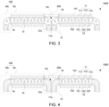
FIG. 3 is a second structural schematic view showing a spliced panel provided by an embodiment of the present disclosure. -
FIG. 4 is a third structural schematic view showing a spliced panel provided by an embodiment of the present disclosure. -
FIG. 5 is a schematic flowchart showing a method of manufacturing a spliced panel provided by an embodiment of the present disclosure. -
FIG. 6 is a fourth structural schematic view showing a spliced panel provided by an embodiment of the present disclosure. - Hereinafter preferred embodiments of the present disclosure will be described with reference to the accompanying drawings to exemplify the embodiments of the present disclosure can be implemented, which can fully describe the technical contents of the present disclosure to make the technical content of the present disclosure clearer and easy to understand. However, the described embodiments are only some of the embodiments of the present disclosure, but not all of the embodiments. All other embodiments obtained by those skilled in the art based on the embodiments of the present disclosure without creative efforts are within the scope of the present disclosure. Embodiments, which are based on the embodiments of the present disclosure, obtained by those skilled in the art without making any inventive efforts are within the scope of protection defined by the present disclosure. It should be noted that described embodiments are merely used to construct the present disclosure and are not intended to limit the present disclosure. In the present disclosure, unless further description is made, terms such as "top" and "bottom" usually refer to a top of a device and a bottom of a device in an actual process or working status, and specifically, to the orientation as shown in the drawings. Terms such as "inside" and "outside" are based on an outline of a device.
- An embodiment of the present provides a spliced panel which is described in detail below. It should be noted that a following description order of embodiments does not denote a preferred description order of the embodiments.
- It should be noted that a spliced
panel 1000 provided by embodiments of the present disclosure as shown inFIGs 1 to 4 includes two display panels disposed in a middle area. This is only an example, and the embodiments are not limited thereto. - Please refer to
FIG. 1 and FIG. 2 , an embodiment of the present disclosure provides the splicedpanel 1000, including at least twodisplay panels 100 and a light-emitting diode (LED)substrate 200. - The at least two
display panels 100 are spliced to each other. Each of the at least twodisplay panels 100 includes a bending part Wz and a non-bending part Nz. The bending part Wz is bent from a side of the non-bending part Nz to a back surface of the at least twodisplay panels 100. The non-bending part Nz is configured to display an image. - In the at least two
display panels 100 spliced to each other, the bending part Wz of one of the at least twodisplay panels 100 is correspondingly spliced to the bending part Wz of another of the at least twodisplay panels 100 to form a support structure Ct. - The
LED substrate 200 is disposed on the support structure Ct. - In the spliced
panel 1000 provided by the present embodiment, part of each of the at least twodisplay panels 100 is bent to form the bending part Wz. Two bending parts Wz are spliced to each other to form the support structure Ct. Then, theLED substrate 200 is disposed on the support structure Ct to cover a splicing gap, thereby preventing the splicing gap from being viewed. In addition, a non-display functional layer of each of the at least twodisplay panels 100 is bent to the back surface of the at least twodisplay panels 100, thereby narrowing a frame. - It should be noted that the back surface of the
display panel 100 is opposite to a display side of thedisplay panel 100. That is, the display side of thedisplay panel 100 is a front surface. - Optionally, the
LED substrate 200 may be a mini LED panel, a micro LED panel, an organic light-emitting diode (OLED) panel, or a quantum-dot light-emitting diode (QLED) panel. - Optionally, the non-bending part Nz is higher than the support structure Ct. In the at least two
display panels 100 spliced to each other, a surface of two non-bending parts Nz and a surface of the support structure Ct form a recess Ho. TheLED substrate 200 is disposed in the recess Ho. - The recess Ho is formed by splicing. The
LED substrate 200 is disposed in the recess Ho, thereby improving flatness of the splicedpanel 1000. - Optionally, a lateral surface of the
LED substrate 200 is connected to the non-bending part Nz by a black adhesive Hj. - The black adhesive Hk is disposed between the lateral surface of the
LED substrate 200 and the non-bending part Nz. Therefore, not only can theLED substrate 200 be stably disposed in the recess Ho, but also a light-shielding effect can be improved. As such, a display contrast can be enhanced. - In some embodiments, the lateral surface of the
LED substrate 200 can be connected to the non-bending part Nz by a non-black adhesive. - Optionally, in the spliced
panel 1000 having a first structure provided by the present embodiment, the at least twodisplay panels 100 are LCD panels, which is taken as a description example. - Each of the at least two
display panels 100 includes afirst substrate 11 and asecond substrate 12 disposed on thefirst substrate 11. - Each of the at least two
display panels 100 further includes aliquid crystal 13 and aframe sealant 14. Theliquid crystal 13 and theframe sealant 14 are disposed between thefirst substrate 11 and thesecond substrate 12. Theframe sealant 14 is disposed surrounding theliquid crystal 13. The non-bending part Nz includes theliquid crystal 13. - The
first substrate 11 includes afirst base 111 and a firstflexible layer 112. The firstflexible layer 112 is disposed on a surface of thefirst base 111 facing thesecond substrate 12. The firstflexible layer 112 includes afirst sub-layer 11a protruding from thefirst base 111. Thefirst sub-layer 11a is bent to be part of the bending part Wz. - In the at least two
display panels 100 spliced to each other, a lateral surface of twofirst bases 111 and a surface of two first sub-layers 11a form the recess Ho. - Optionally, the
second substrate 12 includes asecond base 121, a secondflexible layer 122, and adriving circuit layer 123. The secondflexible layer 122 is disposed on a surface of thesecond base 121 facing thefirst substrate 11. The drivingcircuit layer 123 is disposed on a surface of the secondflexible layer 122 facing thefirst substrate 11. The secondflexible layer 122 includes asecond sub-layer 12a protruding from thesecond base 121. Part of the drivingcircuit layer 123 corresponding to thesecond sub-layer 12a and thesecond sub-layer 12a are bent to be part of the bending part Wz. - Optionally, in a side of the non-bending part Nz close to the bending part Wz, part of the
first base 111 protrudes thesecond base 121, thereby reducing a bending radius of the bending part Wz. - It should be noted that a bending side is the at least two
display panels 100. - Optionally, the bending part Wz includes the
liquid crystal 13. - That is, part of each of the at least two
display panels 100 originally disposed in a display area are the bending part Wz, thereby narrowing a frame. In addition, by setting part of the display area of the at least twodisplay panels 100 to be the bending part Wz, a bending radius of the bending part Wz can be reduced. - Optionally, the
second base 121 may be a simple array substrate, or may be a color filter on array (COA) substrate. The drivingcircuit layer 123 may include a scan line, a data line, a thin-film transistor (TFT), a capacitor, and a pixel electrode, which are disposed on the secondflexible layer 122. Part of the TFT is electrically connected to the pixel electrode. - Optionally, the
first base 111 and thesecond base 121 may be a rigid base or a flexible base. In the present embodiment, thefirst base 111 and thesecond base 121 are the rigid base such as glass, sapphire, or silicon. - Optionally, a material of the first
flexible layer 112 and a material of the secondflexible layer 122 may be selected from one of polystyrene, polylactic acid, polyethylene dicarboxylate, polyethylene terephthalate, polyethylene naphthalate, polycarbonate, polyethersulfone, aromatic fluorine containing polyarylate toluene, polycyclic olefin, polyimide, or polyurethane. - Optionally, the
first substrate 11 further includes ablack matrix layer 113 disposed on a surface of the firstflexible layer 112 facing thesecond substrate 12. A gap jx is defined between theLED substrate 200 and thefirst base 111. - Part of the
black matrix layer 113 covers the gap jx. - Because the bending part Wz is part of the display area, when the at least two
display panels 100 display, the bending part Wz may also display and emit light. TheLED substrate 200 is disposed on the support structure Ct, thereby blocking light emitted from the bending part Wz. The gap jx between theLED substrate 200 and thefirst base 111 is covered by theblack matrix layer 113, thereby preventing light leakage. - Optionally, each of the at least two
display panels 100 further includes afirst polarizer 151 and asecond polarizer 152. Thefirst polarizer 151 is disposed on a surface of thefirst base 111 away from thesecond substrate 12. Thesecond polarizer 152 is disposed on a surface of thesecond base 121 away from thefirst substrate 11. - Please refer to
FIG. 3 . Optionally, differences between an embodiment as shown inFIG. 3 and the above embodiment are: in the present embodiment, the bending part Wz further includes theframe sealant 14. That is, both theliquid crystal 13 and theframe sealant 14 are disposed in the bending part Wz. This structure can increase enlarge the display area of the at least twodisplay panels 100. - Please refer to
FIG. 4 . Optionally, differences between an embodiment as shown inFIG. 4 and the above embodiments are: in the present embodiment, the bending part Wz includes theframe sealant 14, but does not include theliquid crystal 13. That is, in the present embodiment, only part of a non-display area of the splicedpanel 1000 is bent. Therefore, the display area of the at least twodisplay panels 100 is increased, thereby further reducing a risk of light leakage of the splicedpanel 1000. - A method of manufacturing the spliced
panel 1000 of the present embodiment is described below. The at least twodisplay panels 100 are LCD panels, which is taken as a description example. However, the present disclosure is not limited thereto. - Please refer to
FIG. 5 , in the method of manufacturing the splicedpanel 1000 provided by the present embodiment, the splicedpanel 1000 includes twodisplay panels 100 spliced to each other. However, the present disclosure is not limited thereto. The method of manufacturing the splicedpanel 1000 includes following steps: - Step B1, providing at least two display panels. Each of the at least two display panels includes a
first substrate 11 and asecond substrate 12 disposed on thefirst substrate 11. Each of the at least twodisplay panels 100 further includes aliquid crystal 13 and asealant 14. Theliquid crystal 13 and thesealant 14 are disposed between thefirst substrate 11 and thesecond substrate 12. Thesealant 14 is disposed surrounding theliquid crystal 13 to encapsulate theliquid crystal 13. Thefirst substrate 11 includes afirst base 111 and a firstflexible layer 112. The firstflexible layer 112 is disposed on a surface of thefirst base 111 facing thesecond substrate 12. Thesecond substrate 12 includes asecond base 121, a secondflexible layer 122, and adriving circuit layer 123. The secondflexible layer 122 is disposed on a surface of thesecond base 121 facing thefirst substrate 11. A drivingcircuit layer 123 is disposed on a surface of the secondflexible layer 122 facing thefirst substrate 11. - Step B2, respectively cutting part of the
first base 111 and part of thesecond base 121, which correspond to a bending area, thereby making part of the at least twopanels 100 corresponding to the bending area form a bending part Wz that is unfolded. - Step B3, bending the bending part Wz, thereby folding the bending part Wz, and correspondingly splicing the bending parts Wz of the at least two
display panels 100 to each other to form a support structure Ct. - Step B4, disposing an
LED substrate 200 on the support Ct, thereby covering a splicing gap between two bending parts Wz. - Finally, the method of manufacturing the spliced
panel 1000 provided by the present embodiment is completed. - Please refer to
FIG. 6 . Optionally, in some embodiments, the present embodiment provides a splicedpanel 2000, including at least twodisplay panels 100 and anLED substrate 200. - The at least two
display panels 100 are spliced to each other. Each of the at least twodisplay panels 100 includes a bending part Wz and a non-bending part Nz. The bending part Wz is bent from a side of the non-bending part Nz to a back surface of thedisplay panels 100. The non-bending part Nz is configured to display an image. - In the at least two
display panels 100 spliced to each other, the bending part Wz of one of the at least twodisplay panels 100 is correspondingly spliced to the bending part Wz of another of the at least twodisplay panels 100 to form a support structure Ct. - The
LED substrate 200 is disposed on the support structure Ct. - In the spliced
panel 2000 provided by the present embodiment, part of each of the at least twodisplay panels 100 is bent to form the bending part Wz. Two bending parts Wz are spliced to each other to form the support structure Ct. Then, theLED substrate 200 is disposed on the support structure Ct to cover a splicing gap, thereby preventing the splicing gap from being viewed. In addition, a non-display functional layer of each of the at least twodisplay panels 100 is bent to the back surface of the at least twodisplay panels 100, thereby narrowing a frame. - It should be noted that the back surface of the
display panel 100 is opposite to a display side of thedisplay panel 100. That is, the display side of thedisplay panel 100 is a front surface. - Optionally, the
LED substrate 200 may be a mini LED panel, a micro LED panel, an organic light-emitting diode (OLED) panel, or a quantum-dot light-emitting diode (QLED) panel. - Optionally, the non-bending part Nz is higher than the support structure Ct. In the at least two
display panels 100 spliced to each other, a surface of two non-bending parts Nz and a surface of the support structure Ct form a recess Ho. TheLED substrate 200 is disposed in the recess Ho. - The recess Ho is formed by splicing. The
LED substrate 200 is disposed in the recess Ho, thereby improving flatness of the splicedpanel 2000. - Optionally, a lateral surface of the
LED substrate 200 is connected to the non-bending part Nz by a black adhesive Hj. - Optionally, each of the at least two
display panels 100 includes afirst substrate 11 and asecond substrate 12 disposed on thefirst substrate 11. Thefirst substrate 11 is a cover plate. Thesecond substrate 12 includes abase 12c, and aflexible layer 12d, a drivingcircuit layer 12f, a displayfunctional layer 12g, and anencapsulation layer 12h, which are sequentially disposed on thebase 12c. Thefirst substrate 11 is disposed on the displayfunctional layer 12g. Theflexible layer 12d includes a sub-layer 12d1 protruding from thebase 12c. - Optionally, the display
functional layer 12g includes a first electrode, a light-emitting layer, and a second electrode. Optionally, a material of the light-emitting layer may be an organic material or a quantum-dot material. - The
base 12c, part of theflexible layer 12d, part of the drivingcircuit layer 12f, the displayfunctional layer 12g, and thefirst substrate 11 are part of the non-bending part Nz. Part of the drivingcircuit layer 12f corresponding to the sub-layer 12d1 and the sub-layer 12d1 are bent to be part of the bending part Wz. - In the at least two
display panels 100 spliced to each other, an upper surface of the drivingcircuit layer 12f, a lateral surface of twoencapsulation layers 12h, and a lateral surface of twofirst substrates 11 form the recess Ho. - Compared with the above embodiments, the spliced panel of the present embodiment uses LED panels as the at least two
display panels 100. Therefore, it is allowed to only cut part of thebase 12c corresponding to the bending area, thereby simplifying manufacturing steps. - In the present embodiment, the recess Ho has a greater depth. The
LED substrate 200 is disposed in the recess Ho, thereby improving flatness of the splicedpanel 2000. - In addition, a depth of the recess Ho is greater than a thickness of the
LED substrate 200. Therefore, a filling adhesive Tc is filled in the recess Ho to cover theLED substrate 200, thereby protecting and fixing theLED substrate 200. - Optionally, a refractive index of the filling adhesive Tc is equal to a refractive index of the
first substrate 11, thereby reducing a difference between an image displayed by theLED substrate 200 and an image displayed by the at least twodisplay panels 100. - In the spliced panel provided by the present embodiment, each of the at least two display panels is bent to form the bending part, and two bending parts are spliced to each other to form the support structure. Then, the LED substrate is disposed on the support structure, thereby covering a splicing gap. Therefore, the splicing gap will not be viewed. In addition, a non-display functional layer of each of the at least two display panels is bent to the back surface of the at least two display panels, thereby narrowing a frame.
- A spliced panel provided by embodiments of the present disclosure has been described in detail in terms of principles and implementations thereof. However, the description of the above embodiments is only for helping to understand the technical solution of the present disclosure and core ideas thereof, and it is understood by those skilled in the art that many changes and modifications to the described embodiment can be carried out without departing from the scope and the spirit of the disclosure that is intended to be limited only by the appended claims.
Claims (20)
- A spliced panel, comprising:at least two display panels spliced to each other, wherein each of the at least two display panels comprises a bending part and a non-bending part, the bending part is bent from a side of the non-bending part to a back surface of the display panel, the non-bending part is configured to display an image, the bending part of one of the at least two display panels and the bending part of another of the at least two display panels are correspondingly spliced to each other to form a support structure, each of the at least two display panels comprises a first substrate and a second substrate disposed on the first substrate, the first substrate comprises a first base, and the first base is a rigid base or a flexible base; anda light-emitting diode (LED) substrate disposed on the support structure.
- The spliced panel of claim 1, wherein the non-bending part is higher than the support structure, a surface of the non-bending part of the at least two display panels spliced to each other and a surface of the support structure form a recess, and the LED substrate is disposed in the recess.
- The spliced panel of claim 2, wherein a lateral surface of the LED substrate is connected to the non-bending part by a black adhesive.
- The spliced panel of claim 2, wherein the first substrate comprises a first flexible layer, the first flexible layer is disposed on a surface of the first base facing the second substrate, the first flexible layer comprises a first sub-layer protruding from the first base, and the first sub-layer is bent to be part of the bending part; and
a lateral surface of the first base of the at least two display panels spliced to each other and a surface of the first sub-layer of the at least two display panels spliced to each other to form the recess. - The spliced panel of claim 4, wherein a second flexible layer is disposed on a surface of the second base facing the first substrate, a driving circuit layer is disposed on a surface of the second flexible layer facing the first substrate, the second flexible layer comprises a second sub-layer protruding from the second base, and part of the driving circuit layer corresponding to the second sub-layer and the second sub-layer are bent to be part of the bending part.
- The spliced panel of claim 5, wherein each of the at least two display panels comprises a liquid crystal and a frame sealant, the liquid crystal and the frame sealant are disposed between the first substrate and the second substrate, the frame sealant is disposed surrounding the liquid crystal to encapsulate the liquid crystal, and the non-bending part comprises the liquid crystal.
- The spliced panel of claim 6, wherein the bending part comprises the liquid crystal.
- A spliced panel, comprising:at least two display panels spliced to each other, wherein each of the at least two display panels comprises a bending part and a non-bending part, the bending part is bent from a side of the non-bending part to a back surface of the display panel, the non-bending part is configured to display an image, and the bending part of one of the at least two display panels and the bending part of another of the at least two display panels are correspondingly spliced to each other to form a support structure; anda light-emitting diode (LED) substrate disposed on the support structure.
- The spliced panel of claim 8, wherein the non-bending part is higher than the support structure, a surface of the non-bending part of the at least two display panels spliced to each other and a surface of the support structure form a recess, and the LED substrate is disposed in the recess.
- The spliced panel of claim 9, wherein a lateral surface of the LED substrate is connected to the non-bending part by a black adhesive.
- The spliced panel of claim 9, wherein the first substrate comprises a first flexible layer, the first flexible layer is disposed on a surface of the first base facing the second substrate, the first flexible layer comprises a first sub-layer protruding from the first base, and the first sub-layer is bent to be part of the bending part; and
a lateral surface of the first base of the at least two display panels spliced to each other and a surface of the first sub-layer of the at least two display panels spliced to each other to form the recess. - The spliced panel of claim 11, wherein a second flexible layer is disposed on a surface of the second base facing the first substrate, a driving circuit layer is disposed on a surface of the second flexible layer facing the first substrate, the second flexible layer comprises a second sub-layer protruding from the second base, and part of the driving circuit layer corresponding to the second sub-layer and the second sub-layer are bent to be part of the bending part.
- The spliced panel of claim 12, wherein each of the at least two display panels comprises a liquid crystal and a frame sealant, the liquid crystal and the frame sealant are disposed between the first substrate and the second substrate, the frame sealant is disposed surrounding the liquid crystal to encapsulate the liquid crystal, and the non-bending part comprises the liquid crystal.
- The spliced panel of claim 13, wherein the bending part comprises the liquid crystal.
- The spliced panel of claim 14, wherein the bending part comprises the frame sealant.
- The spliced panel of claim 13, wherein the bending part comprises the frame sealant and does not comprise the liquid crystal.
- The spliced panel of claim 14, wherein the first substrate comprises a black matrix layer disposed on a surface of the first flexible layer facing the second substrate, and a gap is defined between the LED substrate and the first base; and
part of the black matrix layer covers the gap. - The spliced panel of claim 9, wherein each of the at least two display panels comprises a first substrate and a second substrate disposed on the first substrate, the first substrate is a cover plate, the second substrate comprises a base, and a flexible layer, a driving circuit layer, a display functional layer, and an encapsulation layer sequentially disposed on the base, the first substrate is disposed on the display functional layer, and the flexible layer comprises a sub-layer protruding from the base;the base, part of the flexible layer, part of the driving circuit layer, part of the display functional layer, part of the encapsulation layer, and the first substrate are part of the non-bending part, and part of the driving circuit layer corresponding to the sub-layer and the sub-layer are bent to be part of the bending part; andin the at least two display panels spliced to each other, an upper surface of two driving circuit layers, a lateral surface of two encapsulation layers, and a lateral surface of two first substrates form the recess.
- The spliced panel of claim 18, wherein a depth of the recess is greater than a thickness of the LED substrate, and a filling adhesive is filled in the recess and covers the LED.
- The spliced panel of claim 19, wherein a refractive index of the filling adhesive is equal to a refractive index of the first substrate.
Applications Claiming Priority (2)
| Application Number | Priority Date | Filing Date | Title |
|---|---|---|---|
| CN202111486712.5A CN114141155B (en) | 2021-12-07 | 2021-12-07 | Spliced panel |
| PCT/CN2021/138912 WO2023103020A1 (en) | 2021-12-07 | 2021-12-16 | Tiled panel |
Publications (2)
| Publication Number | Publication Date |
|---|---|
| EP4447026A1 true EP4447026A1 (en) | 2024-10-16 |
| EP4447026A4 EP4447026A4 (en) | 2025-10-08 |
Family
ID=80384939
Family Applications (1)
| Application Number | Title | Priority Date | Filing Date |
|---|---|---|---|
| EP21827166.6A Pending EP4447026A4 (en) | 2021-12-07 | 2021-12-16 | TILE PANEL |
Country Status (5)
| Country | Link |
|---|---|
| US (1) | US12025873B2 (en) |
| EP (1) | EP4447026A4 (en) |
| JP (1) | JP7590357B2 (en) |
| CN (1) | CN114141155B (en) |
| WO (1) | WO2023103020A1 (en) |
Families Citing this family (4)
| Publication number | Priority date | Publication date | Assignee | Title |
|---|---|---|---|---|
| CN114495731B (en) * | 2022-03-08 | 2024-05-31 | Tcl华星光电技术有限公司 | Display module and display device |
| CN116994490A (en) * | 2022-04-25 | 2023-11-03 | 成都辰显光电有限公司 | Display devices and spliced display devices |
| CN114822273B (en) * | 2022-05-07 | 2022-12-23 | Tcl华星光电技术有限公司 | splice panel |
| CN115083297A (en) | 2022-07-05 | 2022-09-20 | Tcl华星光电技术有限公司 | Spliced display panel |
Family Cites Families (22)
| Publication number | Priority date | Publication date | Assignee | Title |
|---|---|---|---|---|
| US20020163301A1 (en) | 2001-05-02 | 2002-11-07 | Morley Roland M. | Large format emissive display |
| JP2005031247A (en) | 2003-07-09 | 2005-02-03 | Seiko Epson Corp | Image display device |
| CN104464557B (en) | 2013-09-24 | 2019-07-12 | 夏展敏 | A kind of edge shows the scheme integrated with liquid crystal display |
| KR102272216B1 (en) * | 2015-02-13 | 2021-07-02 | 삼성디스플레이 주식회사 | tiled display apparatus |
| CN105448198A (en) * | 2016-01-04 | 2016-03-30 | 京东方科技集团股份有限公司 | Splicing screen, manufacturing method thereof, and display device |
| CN207353253U (en) | 2017-04-14 | 2018-05-11 | 深圳市微阵技术有限公司 | Rimless shows bar and screen splicing system |
| US10593746B2 (en) * | 2017-10-30 | 2020-03-17 | Wuhan China Star Optoelectronics Technology Co., Ltd. | Spliced display device |
| US11322489B2 (en) | 2019-01-31 | 2022-05-03 | Innolux Corporation | Tiled display device |
| CN112309245B (en) * | 2019-07-26 | 2022-08-23 | 群创光电股份有限公司 | Foldable display device |
| KR102648809B1 (en) * | 2019-09-11 | 2024-03-20 | 삼성디스플레이 주식회사 | Display device and tiled display device having the same |
| CN113160701B (en) | 2020-01-22 | 2023-03-07 | 群创光电股份有限公司 | Video wall |
| CN111290154A (en) | 2020-02-24 | 2020-06-16 | 京东方科技集团股份有限公司 | Display device and spliced screen |
| WO2021189433A1 (en) * | 2020-03-27 | 2021-09-30 | 京东方科技集团股份有限公司 | Strip-shaped display structure, display panel and display device |
| CN111369900A (en) * | 2020-04-07 | 2020-07-03 | 深圳市华星光电半导体显示技术有限公司 | Spliced screen |
| CN212161167U (en) * | 2020-05-13 | 2020-12-15 | 深圳雷曼光电科技股份有限公司 | Display device and display screen |
| CN111584475B (en) * | 2020-05-15 | 2021-11-23 | 深圳市华星光电半导体显示技术有限公司 | Spliced display panel and preparation method thereof |
| CN111653207B (en) * | 2020-07-30 | 2022-12-13 | 上海天马微电子有限公司 | Display module assembly, display device and spliced screen |
| CN112382212B (en) | 2020-12-03 | 2021-12-03 | 深圳市华星光电半导体显示技术有限公司 | Display panel, manufacturing method of display panel and display screen |
| CN113031338A (en) | 2021-03-22 | 2021-06-25 | 惠州视维新技术有限公司 | TFT-LCD display panel, manufacturing method thereof and display device |
| CN113160714A (en) | 2021-04-22 | 2021-07-23 | 京东方科技集团股份有限公司 | Spliced screen and preparation method thereof |
| CN113703211B (en) | 2021-08-16 | 2023-02-03 | Tcl华星光电技术有限公司 | Tiled display device |
| CN113658518B (en) | 2021-08-24 | 2023-07-04 | 京东方科技集团股份有限公司 | Display panel, preparation method thereof and display device |
-
2021
- 2021-12-07 CN CN202111486712.5A patent/CN114141155B/en active Active
- 2021-12-16 US US17/622,800 patent/US12025873B2/en active Active
- 2021-12-16 EP EP21827166.6A patent/EP4447026A4/en active Pending
- 2021-12-16 WO PCT/CN2021/138912 patent/WO2023103020A1/en not_active Ceased
- 2021-12-16 JP JP2021576694A patent/JP7590357B2/en active Active
Also Published As
| Publication number | Publication date |
|---|---|
| US12025873B2 (en) | 2024-07-02 |
| EP4447026A4 (en) | 2025-10-08 |
| WO2023103020A1 (en) | 2023-06-15 |
| CN114141155B (en) | 2023-06-30 |
| CN114141155A (en) | 2022-03-04 |
| JP7590357B2 (en) | 2024-11-26 |
| JP2024503157A (en) | 2024-01-25 |
| US20240036376A1 (en) | 2024-02-01 |
Similar Documents
| Publication | Publication Date | Title |
|---|---|---|
| US12025873B2 (en) | Spliced panel | |
| US10175548B2 (en) | Display device, manufacturing method thereof, driving method thereof, and display apparatus | |
| KR101957998B1 (en) | Display panel and method of fabricating the same | |
| KR102077525B1 (en) | Display device and method of manufacturing the same | |
| KR100925312B1 (en) | Electro-optical device, method of manufacturing electro-optical device, and electronic apparatus | |
| US8963897B2 (en) | Display device with pixels of differing display types and fabrication method thereof | |
| JP4007308B2 (en) | Electro-optical device, electronic apparatus, and method of manufacturing electro-optical device | |
| US10651130B2 (en) | Display device | |
| US20120098739A1 (en) | Spliced electrophoretic display panel | |
| KR20100002816A (en) | Liquid crystal display | |
| KR20160056460A (en) | Curved display device | |
| KR20260046356A (en) | Display apparatus | |
| KR102648809B1 (en) | Display device and tiled display device having the same | |
| JP2010224081A (en) | Display device | |
| CN212461009U (en) | Display screen, spliced display screen and display device | |
| JP2009223219A (en) | Electrooptical device and electronic apparatus | |
| KR101667055B1 (en) | Display Device And Manufacturing Method Of The Same | |
| KR101995778B1 (en) | Liquid crystal display device | |
| KR102575599B1 (en) | Flexible display panel and method of fabricating the same | |
| JP2010060883A (en) | Display device | |
| CN119126420A (en) | Display module and spliced display device | |
| JP2011082098A (en) | Organic el device, electro-optical device, and electronic apparatus | |
| CN119335771A (en) | Display device with switchable viewing angle | |
| KR102123947B1 (en) | Multi panel display device | |
| JP6620548B2 (en) | Display device |
Legal Events
| Date | Code | Title | Description |
|---|---|---|---|
| STAA | Information on the status of an ep patent application or granted ep patent |
Free format text: STATUS: UNKNOWN |
|
| STAA | Information on the status of an ep patent application or granted ep patent |
Free format text: STATUS: THE INTERNATIONAL PUBLICATION HAS BEEN MADE |
|
| PUAI | Public reference made under article 153(3) epc to a published international application that has entered the european phase |
Free format text: ORIGINAL CODE: 0009012 |
|
| STAA | Information on the status of an ep patent application or granted ep patent |
Free format text: STATUS: REQUEST FOR EXAMINATION WAS MADE |
|
| 17P | Request for examination filed |
Effective date: 20211227 |
|
| AK | Designated contracting states |
Kind code of ref document: A1 Designated state(s): AL AT BE BG CH CY CZ DE DK EE ES FI FR GB GR HR HU IE IS IT LI LT LU LV MC MK MT NL NO PL PT RO RS SE SI SK SM TR |
|
| DAV | Request for validation of the european patent (deleted) | ||
| DAX | Request for extension of the european patent (deleted) | ||
| A4 | Supplementary search report drawn up and despatched |
Effective date: 20250910 |
|
| RIC1 | Information provided on ipc code assigned before grant |
Ipc: G09F 9/302 20060101AFI20250904BHEP Ipc: G09F 9/30 20060101ALI20250904BHEP Ipc: G02F 1/1333 20060101ALI20250904BHEP Ipc: G09F 9/33 20060101ALI20250904BHEP Ipc: G09F 9/35 20060101ALI20250904BHEP |