EP4446808A2 - Optisches faserwellenleitersystem und verfahren zu seiner herstellung - Google Patents
Optisches faserwellenleitersystem und verfahren zu seiner herstellung Download PDFInfo
- Publication number
- EP4446808A2 EP4446808A2 EP24196755.3A EP24196755A EP4446808A2 EP 4446808 A2 EP4446808 A2 EP 4446808A2 EP 24196755 A EP24196755 A EP 24196755A EP 4446808 A2 EP4446808 A2 EP 4446808A2
- Authority
- EP
- European Patent Office
- Prior art keywords
- core
- waveguide
- guide
- plasmonic
- optical
- Prior art date
- Legal status (The legal status is an assumption and is not a legal conclusion. Google has not performed a legal analysis and makes no representation as to the accuracy of the status listed.)
- Withdrawn
Links
Images


Classifications
-
- H—ELECTRICITY
- H01—ELECTRIC ELEMENTS
- H01S—DEVICES USING THE PROCESS OF LIGHT AMPLIFICATION BY STIMULATED EMISSION OF RADIATION [LASER] TO AMPLIFY OR GENERATE LIGHT; DEVICES USING STIMULATED EMISSION OF ELECTROMAGNETIC RADIATION IN WAVE RANGES OTHER THAN OPTICAL
- H01S3/00—Lasers, i.e. devices using stimulated emission of electromagnetic radiation in the infrared, visible or ultraviolet wave range
- H01S3/05—Construction or shape of optical resonators; Accommodation of active medium therein; Shape of active medium
- H01S3/06—Construction or shape of active medium
- H01S3/063—Waveguide lasers, i.e. whereby the dimensions of the waveguide are of the order of the light wavelength
- H01S3/067—Fibre lasers
- H01S3/06708—Constructional details of the fibre, e.g. compositions, cross-section, shape or tapering
- H01S3/06729—Peculiar transverse fibre profile
-
- H—ELECTRICITY
- H01—ELECTRIC ELEMENTS
- H01S—DEVICES USING THE PROCESS OF LIGHT AMPLIFICATION BY STIMULATED EMISSION OF RADIATION [LASER] TO AMPLIFY OR GENERATE LIGHT; DEVICES USING STIMULATED EMISSION OF ELECTROMAGNETIC RADIATION IN WAVE RANGES OTHER THAN OPTICAL
- H01S3/00—Lasers, i.e. devices using stimulated emission of electromagnetic radiation in the infrared, visible or ultraviolet wave range
- H01S3/09—Processes or apparatus for excitation, e.g. pumping
- H01S3/091—Processes or apparatus for excitation, e.g. pumping using optical pumping
- H01S3/094—Processes or apparatus for excitation, e.g. pumping using optical pumping by coherent light
- H01S3/094076—Pulsed or modulated pumping
-
- G—PHYSICS
- G02—OPTICS
- G02B—OPTICAL ELEMENTS, SYSTEMS OR APPARATUS
- G02B5/00—Optical elements other than lenses
- G02B5/008—Surface plasmon devices
-
- G—PHYSICS
- G02—OPTICS
- G02B—OPTICAL ELEMENTS, SYSTEMS OR APPARATUS
- G02B6/00—Light guides; Structural details of arrangements comprising light guides and other optical elements, e.g. couplings
- G02B6/02—Optical fibres with cladding with or without a coating
- G02B6/02057—Optical fibres with cladding with or without a coating comprising gratings
- G02B6/02061—Grating external to the fibre and in contact with the fibre, e.g. evanescently coupled, gratings applied to the fibre end
-
- G—PHYSICS
- G02—OPTICS
- G02B—OPTICAL ELEMENTS, SYSTEMS OR APPARATUS
- G02B6/00—Light guides; Structural details of arrangements comprising light guides and other optical elements, e.g. couplings
- G02B6/10—Light guides; Structural details of arrangements comprising light guides and other optical elements, e.g. couplings of the optical waveguide type
- G02B6/12—Light guides; Structural details of arrangements comprising light guides and other optical elements, e.g. couplings of the optical waveguide type of the integrated circuit kind
- G02B6/122—Basic optical elements, e.g. light-guiding paths
- G02B6/1226—Basic optical elements, e.g. light-guiding paths involving surface plasmon interaction
-
- G—PHYSICS
- G02—OPTICS
- G02B—OPTICAL ELEMENTS, SYSTEMS OR APPARATUS
- G02B6/00—Light guides; Structural details of arrangements comprising light guides and other optical elements, e.g. couplings
- G02B6/24—Coupling light guides
- G02B6/26—Optical coupling means
- G02B6/28—Optical coupling means having data bus means, i.e. plural waveguides interconnected and providing an inherently bidirectional system by mixing and splitting signals
- G02B6/293—Optical coupling means having data bus means, i.e. plural waveguides interconnected and providing an inherently bidirectional system by mixing and splitting signals with wavelength selective means
- G02B6/29304—Optical coupling means having data bus means, i.e. plural waveguides interconnected and providing an inherently bidirectional system by mixing and splitting signals with wavelength selective means operating by diffraction, e.g. grating
- G02B6/29316—Light guides comprising a diffractive element, e.g. grating in or on the light guide such that diffracted light is confined in the light guide
- G02B6/29323—Coupling to or out of the diffractive element through the lateral surface of the light guide
-
- H—ELECTRICITY
- H01—ELECTRIC ELEMENTS
- H01S—DEVICES USING THE PROCESS OF LIGHT AMPLIFICATION BY STIMULATED EMISSION OF RADIATION [LASER] TO AMPLIFY OR GENERATE LIGHT; DEVICES USING STIMULATED EMISSION OF ELECTROMAGNETIC RADIATION IN WAVE RANGES OTHER THAN OPTICAL
- H01S3/00—Lasers, i.e. devices using stimulated emission of electromagnetic radiation in the infrared, visible or ultraviolet wave range
- H01S3/05—Construction or shape of optical resonators; Accommodation of active medium therein; Shape of active medium
- H01S3/06—Construction or shape of active medium
- H01S3/063—Waveguide lasers, i.e. whereby the dimensions of the waveguide are of the order of the light wavelength
- H01S3/067—Fibre lasers
- H01S3/06708—Constructional details of the fibre, e.g. compositions, cross-section, shape or tapering
- H01S3/06725—Fibre characterized by a specific dispersion, e.g. for pulse shaping in soliton lasers or for dispersion compensating [DCF]
-
- H—ELECTRICITY
- H01—ELECTRIC ELEMENTS
- H01S—DEVICES USING THE PROCESS OF LIGHT AMPLIFICATION BY STIMULATED EMISSION OF RADIATION [LASER] TO AMPLIFY OR GENERATE LIGHT; DEVICES USING STIMULATED EMISSION OF ELECTROMAGNETIC RADIATION IN WAVE RANGES OTHER THAN OPTICAL
- H01S3/00—Lasers, i.e. devices using stimulated emission of electromagnetic radiation in the infrared, visible or ultraviolet wave range
- H01S3/09—Processes or apparatus for excitation, e.g. pumping
- H01S3/091—Processes or apparatus for excitation, e.g. pumping using optical pumping
- H01S3/094—Processes or apparatus for excitation, e.g. pumping using optical pumping by coherent light
- H01S3/094003—Processes or apparatus for excitation, e.g. pumping using optical pumping by coherent light the pumped medium being a fibre
- H01S3/094019—Side pumped fibre, whereby pump light is coupled laterally into the fibre via an optical component like a prism, or a grating, or via V-groove coupling
-
- H—ELECTRICITY
- H01—ELECTRIC ELEMENTS
- H01S—DEVICES USING THE PROCESS OF LIGHT AMPLIFICATION BY STIMULATED EMISSION OF RADIATION [LASER] TO AMPLIFY OR GENERATE LIGHT; DEVICES USING STIMULATED EMISSION OF ELECTROMAGNETIC RADIATION IN WAVE RANGES OTHER THAN OPTICAL
- H01S3/00—Lasers, i.e. devices using stimulated emission of electromagnetic radiation in the infrared, visible or ultraviolet wave range
- H01S3/09—Processes or apparatus for excitation, e.g. pumping
- H01S3/091—Processes or apparatus for excitation, e.g. pumping using optical pumping
- H01S3/094—Processes or apparatus for excitation, e.g. pumping using optical pumping by coherent light
- H01S3/0941—Processes or apparatus for excitation, e.g. pumping using optical pumping by coherent light of a laser diode
-
- H—ELECTRICITY
- H01—ELECTRIC ELEMENTS
- H01S—DEVICES USING THE PROCESS OF LIGHT AMPLIFICATION BY STIMULATED EMISSION OF RADIATION [LASER] TO AMPLIFY OR GENERATE LIGHT; DEVICES USING STIMULATED EMISSION OF ELECTROMAGNETIC RADIATION IN WAVE RANGES OTHER THAN OPTICAL
- H01S3/00—Lasers, i.e. devices using stimulated emission of electromagnetic radiation in the infrared, visible or ultraviolet wave range
- H01S3/05—Construction or shape of optical resonators; Accommodation of active medium therein; Shape of active medium
- H01S3/06—Construction or shape of active medium
- H01S3/063—Waveguide lasers, i.e. whereby the dimensions of the waveguide are of the order of the light wavelength
- H01S3/067—Fibre lasers
- H01S3/06708—Constructional details of the fibre, e.g. compositions, cross-section, shape or tapering
- H01S3/06729—Peculiar transverse fibre profile
- H01S3/06737—Fibre having multiple non-coaxial cores, e.g. multiple active cores or separate cores for pump and gain
-
- H—ELECTRICITY
- H01—ELECTRIC ELEMENTS
- H01S—DEVICES USING THE PROCESS OF LIGHT AMPLIFICATION BY STIMULATED EMISSION OF RADIATION [LASER] TO AMPLIFY OR GENERATE LIGHT; DEVICES USING STIMULATED EMISSION OF ELECTROMAGNETIC RADIATION IN WAVE RANGES OTHER THAN OPTICAL
- H01S3/00—Lasers, i.e. devices using stimulated emission of electromagnetic radiation in the infrared, visible or ultraviolet wave range
- H01S3/05—Construction or shape of optical resonators; Accommodation of active medium therein; Shape of active medium
- H01S3/06—Construction or shape of active medium
- H01S3/063—Waveguide lasers, i.e. whereby the dimensions of the waveguide are of the order of the light wavelength
- H01S3/067—Fibre lasers
- H01S3/0675—Resonators including a grating structure, e.g. distributed Bragg reflectors [DBR] or distributed feedback [DFB] fibre lasers
Definitions
- the present disclosure relates to optical fibers, and more particularly to systems and methods for controlling optical fiber properties through the use of plasmonic structures formed or secured on an optical fiber.
- Plasmonic light-waves are electromagnetic waves propagating on metal surfaces coupled with surface electron oscillations.
- the coupling to electron oscillations enables extreme modifications to the propagating light, but this comes at a price of enhanced attenuation.
- careful design of complex metal-optic structures is a key-enabler for many ground breaking technologies. Merging plasmonics and optical fiber technologies has been previously explored, but primarily for sensing applications.
- an optical waveguide system may include a first waveguide having a core-guide and a material portion surrounding and encasing the core-guide, the core-guide enabling a core-guide mode for an optical signal travelling through the core-guide.
- a second waveguide may be included which forms a lossy waveguide. The construction of the second waveguide is such as to achieve a desired coupling between the core-guide mode and the lossy waveguide to control an energy level of the optical signal travelling through the core-guide.
- the present disclosure relates to a surface emitting fiber laser including an optical fiber forming a first waveguide, and having a core-guide and a material portion surrounding and encasing the core-guide, the core-guide enabling a core-guide mode for an optical signal travelling through the core-guide.
- a second waveguide may be included which is formed from metal secured to an outer surface of the first waveguide.
- the second waveguide forms a plasmonic device which implements a plasmonic mode waveguide.
- the construction of the second waveguide is such as to achieve a desired coupling between the core-guide mode and the plasmonic mode waveguide.
- An optical pump source may be included for injecting optical pump energy into the core-guide via the coupling between the plasmonic device and the core-guide.
- the present disclosure relates to a method for forming an optical waveguide.
- the method may include providing a first waveguide having a core-guide and a material portion surrounding and encasing the core-guide, the core-guide enabling a core-guide mode for an optical signal travelling through the core-guide.
- the method may further include disposing a second waveguide, formed from metal, on an outer surface of the first waveguide, the second waveguide forming a plasmonic device which implements a plasmonic mode waveguide.
- the method may further include using the second waveguide to achieve a desired coupling between the core-guide mode and the plasmonic mode waveguide to control an energy level of the optical signal travelling through the core-guide.
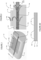
- the system 10 may comprise a length of D-shaped optical fiber 12 having a cladding 12a with a flat surface portion 12b, and a core-guide 12c encased within the cladding 12a.
- the core-guide 12c is a glass fiber that enables a core-guide mode when an optical input signal 16 is input into the core-guide 12c.
- a relatively thin metal layer 14 is secured or formed thereon on the flat surface portion 12b of the cladding 12a.
- the thin metal layer 14 forms a plasmonic device (hereinafter "plasmonic device 14"), which supports a plasmonic mode when the optical signal 16 is travelling through the core-guide 12c.
- the core-to-fiber surface distance is reduced in a specific region, as indicated by dimension D1 in the side cross sectional view of Figure 2 , enabling the enhanced coupling to the plasmonic device 14.
- the thin metal layer which forms the plasmonic device 14 may be, for example, constructed from, for example and without limitation, gold (Au), silver (Ag) or copper (Cu), and be on the order of between about tens of nanometers to hundreds of nanometers in thickness, or possibly even thicker.
- the plasmonic device 14 forms a lattice-like structure having a plurality of spaced apart strips 14a which form grooves 14b therebetween.
- the grooves 14b in this example are formed normal to a longitudinal axis of the core-guide, indicated by line "A" in Figure 2 .
- the strips 14a in this example may be spaced apart by a distance of up to hundreds of micrometers, or possibly even greater, and each strip has a width that will be selected based on the specific application, in one example up to hundreds of micrometers in width, or possibly even greater.
- the thin metal layer forming the plasmonic device 14 may have no grooves at all.
- the plasmonic device 14 may be created/applied through any suitable, well-known process, for example, by masked evaporation, sputtering, lithography or even controlled plating.
- the plasmonic device 14 supports a plasmonic local mode (or alternatively a lossy waveguide made with absorbing medium).
- a plasmonic local mode or alternatively a lossy waveguide made with absorbing medium.
- the energy level of the optical signal 16 travelling through the core-guide 12c can be controlled (and will usually depend on the optical frequency), such as, for example, to create a controlled spectral transmission.
- the controlled spectral transmission may be used to controllably attenuate the optical signal travelling through the core-guide 12c.
- One valuable application of the system 10 may be as a frequency notch filter.
- the propagation in an optical fiber could be simplistically viewed in a ray optics description as a ray zig-zag bouncing inside the fiber due to total internal refractions.
- the ray propagation angle is different (representative of the waveguide modal wavenumber, k-vector).
- the curve that details the k-vector of the propagating mode as a function of the frequency is the dispersion curve characterizing the waveguide.
- the metal layer forming the plasmonic device 14 i.e., being a plasmonic waveguide
- the two waveguides i.e., plasmonic device 14 and core-guide 12c
- the coupling between their modes is created, and at certain frequencies the angle of propagation of the two matches better, which results in enhanced coupling (i.e., more optical energy transferred to the plasmonic device 14, as indicated by waveform 16a in Figure 2 ).
- the attenuation of the propagating mode will therefore be enhanced, resulting in a notch filter. Since the notch location depends on structural properties, this sets the basis for a pulse spectrum reshaping scheme by cascading two or more filters.
- fast pedestal suppression function (at the speed of the nonlinear effect) can be achieved.
- the "pedestal” referred to represents the lower intensity parts of the pulse away from its central peak.
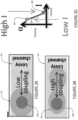
- the fast pedestal suppression is shown 3A.
- Figure 3C also shows that at high intensity, indicated by point 20, for the coupling of Figure 3A , fast pedestal suppression is achieved.
- the coupling at low intensity is set to be high, resulting in a low transmission from the core-guide mode 12c to the plasmonic device 14.
- the coupling, " ⁇ " is designed to be reduced by the change in the nonlinear index between the two waveguides - resulting in increased transmission, as shown in Figure 3C by the curve 22 and the difference between the low intensity point 24 and the high intensity point 20.
- the system 10 is thus implementing a pedestal suppression function, and the details of the function are being set by the nonlinear optical coupling scheme between the two waveguides formed by the core-guide 12c and the plasmonic device 14.
- Such a "passive optical valve” component can improve the contrast between the "ON" state and the noise level.
- the nonlinearity would result from the deposited nonlinear material layer making up the plasmonic device 14 or from the metal nonlinearity itself.
- This concept of designing a nonlinear optical transmission function to an optical fiber segment could be further explored to obtain other complex transmission shapes, for example by depositing plasmonic cavities onto the flat surface of the D-shaped fiber instead of a uniform thickness metal layer, which adds dispersion curve resonances.
- An additional example is a saturable absorber function resulting in a flat top shaped pulse.
- the above teachings for designing the nonlinear transmission could be further extended to affecting the accumulated phase. Similar to how spatially modifying the index (e.g., lens), and thus spatially the accumulated phase, could reshape the light spatially, temporal reshaping of the phase could reshape the pulse in time.
- the coupling between the two waveguides formed by the core-guide 12c and the plasmonic device 14 modifies the intensity profile and, due to the optical nonlinearity, results in a modified refractive index.
- the net modal index (related to the phase accumulation of the propagating mode) could be estimated as the overlap integral of the modified refractive index and the field distribution shape.
- a b-integral compensator could be implemented using KTP crystal near the phase matching angle (through a cascaded vic-2 nonlinearity).
- the system 10, modified as described above, would have the advantage of being an in-fiber integrated device, and have the wavelength configurability based on the design.
- Still another function that could be tailored using the system 10, which forms plasmonic fibers, is unique fiber dispersion. As shown in Figure 3D , this optional configuration could be achieved by forming resonant cavities 18 deposited onto the flat surface 12b of the D-shaped fiber 12, and could be even further enhanced by strong coupling of plasmonic structures and cavities with excitons in dye molecules and quantum dots.
- the dye molecules are lossy at a given narrow band wavelength, and could replace the metal material as the lossy media, or alternatively could be added to it, to thus reshape the response.
- the optical fiber 100 includes a cladding 100a having a core-guide mode 100b and an outer surface portion 100c.
- a carefully designed sub-wavelength metal array 102, having grooves 102a, is known to enable a maximum constructive interference in the far-field, that is, in the direction normal to the optical fiber 100 (i.e., indicated by arrows 104), which has been demonstrated for laser diodes facets.
- the angle may be tuned as needed to meet a specific application; in other words the angle does not have to be normal to the optical fiber 100.
- the side emitting plasmonic section formed by the metal array 102 could be repeated along the length of the optical fiber 100 to create an array of emitters for emitting optical energy. Furthermore, each emitter could exhibit a different phase in a controllable way, resulting in a phased array controlled beam.
- Figure 5 shows an embodiment of an optical fiber 200 coiled with a plurality of aligned, side emitting segments metal segments 202 for emitting optical energy, such as shown in Figure 4 , which form plasmonic devices. Coiling of the optical fiber 200 creates a two dimensional array of coherently added lasers, with total emitter area much larger than the area of the fiber core-guide 12c.
- Another potential modification may be the addition of a mirror 106, as shown in Figures 6 and 7 , near the side emitter of the metal array 102.
- the lens-like shape of the D-shaped fiber cross-section 100a of the optical fiber 100 may be used to couple the normal-to-fiber radiation 103, from a pump source 108, for example a broad area diode laser, which is controlled by an electronic controller 109, into a fiber propagating mode (i.e., into a core-guide mode).
- a pump source 108 for example a broad area diode laser, which is controlled by an electronic controller 109
- Broad-area laser diodes have been recently proposed to set attractive pumping sources for fiber lasers due to their relatively high power ( ⁇ 10W).
- the fiber coupled broad area diode configuration shown in Figures 6 and 7 is expected to be of high interest as a pumping scheme since it allows coupling of the pump light from one or more optical pump sources into the longitudinally propagating light 110 in the core-guide 100c of the optical fiber 100.
- This configuration furthermore enables combining the power of several pump sources 108 providing optical pump energy 108a at spaced apart locations along the length of an optical fiber 100, as shown in the embodiment of Figure 8 .
- Surface emitting fiber lasers have been suggested in previous work but have typically involved using a complex structure of hollow core fiber filled with a gain medium and radial dielectric multi-layer side walls.
- the system shown in Figure 6 is constructed with significantly fewer component elements and allows for spatial control of the emitted beam.
- the various embodiments described herein enable control over optical fiber properties by patterning a plasmonic structure (or plasmonic structures) directly onto optical fibers.
- a plasmonic structure or plasmonic structures
- Using the strong light-matter interaction of plasmonics enables the design of unique pulse shaping functions and/or filtering to be achieved, as well as allowing for the construction of side emitting and pumping of fiber lasers.
- first, second, third, etc. may be used herein to describe various elements, components, regions, layers and/or sections, these elements, components, regions, layers and/or sections should not be limited by these terms. These terms may be only used to distinguish one element, component, region, layer or section from another region, layer or section. Terms such as “first,” “second,” and other numerical terms when used herein do not imply a sequence or order unless clearly indicated by the context. Thus, a first element, component, region, layer or section discussed below could be termed a second element, component, region, layer or section without departing from the teachings of the example embodiments.
- spatially relative terms such as “inner,” “outer,” “beneath,” “below,” “lower,” “above,” “upper,” and the like, may be used herein for ease of description to describe one element or feature's relationship to another element(s) or feature(s) as illustrated in the figures.
- Spatially relative terms may be intended to encompass different orientations of the device in use or operation in addition to the orientation depicted in the figures. For example, if the device in the figures is turned over, elements described as “below” or “beneath” other elements or features would then be oriented “above” the other elements or features.
- the example term “below” can encompass both an orientation of above and below.
- the device may be otherwise oriented (rotated 90 degrees or at other orientations) and the spatially relative descriptors used herein interpreted accordingly.
- optical waveguide system including:
- the second waveguide comprises metal which forms a plasmonic device, and which implements a plasmonic mode waveguide.
- the material portion surrounding the core-guide includes a flat surface portion, and the plasmonic device is disposed on the flat surface portion.
- the core-guide has a D-shaped construction when viewed in cross section.
- the plasmonic device comprises a lattice like structure having a plurality of spaced apart strips.
- the plasmonic device is formed by a plurality of metal sections with grooves formed therein, the grooves opening normal to the core-guide, and the plasmonic device forming an emitter for emitting optical energy.
- the diode comprises a broad area diode.
- the core-guide is arranged in a coil
- the plasmonic device includes a plurality of independent plasmonic devices aligned adjacent to one another on the outer surface, which collectively form a two dimensional emitter.
- the plasmonic device is constructed from at least one of:
- the invention may be also summarized as a surface emitting fiber laser including:
- the surface emitting fiber laser further comprising a plurality of optical pump sources disposed along a length of the optical fiber.
- the previous surface emitting fiber laser further comprising a plurality of mirrors, one mirror of said plurality of mirrors being associated with each said optical pump source.
- the invention may be also summarized a method for forming an optical waveguide, including:
Landscapes
- Physics & Mathematics (AREA)
- Electromagnetism (AREA)
- Optics & Photonics (AREA)
- Engineering & Computer Science (AREA)
- Plasma & Fusion (AREA)
- General Physics & Mathematics (AREA)
- Microelectronics & Electronic Packaging (AREA)
- Optical Couplings Of Light Guides (AREA)
- Optical Modulation, Optical Deflection, Nonlinear Optics, Optical Demodulation, Optical Logic Elements (AREA)
- Optical Integrated Circuits (AREA)
Applications Claiming Priority (3)
| Application Number | Priority Date | Filing Date | Title |
|---|---|---|---|
| US16/037,837 US10756503B2 (en) | 2018-07-17 | 2018-07-17 | System and method for plasmonic control of short pulses in optical fibers |
| EP19838026.3A EP3807692B1 (de) | 2018-07-17 | 2019-07-17 | Optisches faserwellenleitersystem und dessen herstellungsverfahren |
| PCT/US2019/042266 WO2020018706A1 (en) | 2018-07-17 | 2019-07-17 | System and method for plasmonic control of short pulses in optical fibers |
Related Parent Applications (2)
| Application Number | Title | Priority Date | Filing Date |
|---|---|---|---|
| EP19838026.3A Division-Into EP3807692B1 (de) | 2018-07-17 | 2019-07-17 | Optisches faserwellenleitersystem und dessen herstellungsverfahren |
| EP19838026.3A Division EP3807692B1 (de) | 2018-07-17 | 2019-07-17 | Optisches faserwellenleitersystem und dessen herstellungsverfahren |
Publications (2)
| Publication Number | Publication Date |
|---|---|
| EP4446808A2 true EP4446808A2 (de) | 2024-10-16 |
| EP4446808A3 EP4446808A3 (de) | 2025-01-01 |
Family
ID=69161244
Family Applications (2)
| Application Number | Title | Priority Date | Filing Date |
|---|---|---|---|
| EP24196755.3A Withdrawn EP4446808A3 (de) | 2018-07-17 | 2019-07-17 | Optisches faserwellenleitersystem und verfahren zu seiner herstellung |
| EP19838026.3A Active EP3807692B1 (de) | 2018-07-17 | 2019-07-17 | Optisches faserwellenleitersystem und dessen herstellungsverfahren |
Family Applications After (1)
| Application Number | Title | Priority Date | Filing Date |
|---|---|---|---|
| EP19838026.3A Active EP3807692B1 (de) | 2018-07-17 | 2019-07-17 | Optisches faserwellenleitersystem und dessen herstellungsverfahren |
Country Status (3)
| Country | Link |
|---|---|
| US (2) | US10756503B2 (de) |
| EP (2) | EP4446808A3 (de) |
| WO (1) | WO2020018706A1 (de) |
Families Citing this family (2)
| Publication number | Priority date | Publication date | Assignee | Title |
|---|---|---|---|---|
| US11204466B2 (en) * | 2019-11-22 | 2021-12-21 | Corning Research & Development Corporation | Optical fiber photonic integrated chip connector interfaces, photonic integrated chip assemblies, and methods of fabricating the same |
| WO2021243266A1 (en) * | 2020-05-29 | 2021-12-02 | Baylor University | Tunable nanocircuit and waveguide system and method on optical fiber |
Family Cites Families (9)
| Publication number | Priority date | Publication date | Assignee | Title |
|---|---|---|---|---|
| US5444723A (en) * | 1993-08-18 | 1995-08-22 | Institut National D'optique | Optical switch and Q-switched laser |
| US5729641A (en) * | 1996-05-30 | 1998-03-17 | Sdl, Inc. | Optical device employing edge-coupled waveguide geometry |
| CN101910935A (zh) | 2007-11-19 | 2010-12-08 | 哈佛大学的校长及成员们 | 改进辐射束准直的方法和装置 |
| US7920766B2 (en) * | 2009-02-10 | 2011-04-05 | Alcatel-Lucent Usa Inc. | Surface-plasmon-assisted optical frequency conversion |
| US8233358B2 (en) | 2009-06-15 | 2012-07-31 | Headway Technologies, Inc. | Plasmon antenna with magnetic core for thermally assisted magnetic recording |
| US8908189B2 (en) * | 2011-04-15 | 2014-12-09 | Carl Zeiss Meditec, Inc. | Systems and methods for swept-source optical coherence tomography |
| US9459163B2 (en) | 2013-01-22 | 2016-10-04 | The Regents Of The University Of California | Ultra-sensitive force sensing based on evanescent light |
| EP3096131A1 (de) * | 2015-05-18 | 2016-11-23 | International Iberian Nanotechnology Laboratory | Optische faser zur verwendung in einem system zur detektion einer oder mehrerer verbindungen in einer flüssigkeit |
| WO2018118807A1 (en) | 2016-12-19 | 2018-06-28 | Lawrence Livermore National Security, Llc | Wavelength selective transfer of optical energy |
-
2018
- 2018-07-17 US US16/037,837 patent/US10756503B2/en active Active
-
2019
- 2019-07-17 WO PCT/US2019/042266 patent/WO2020018706A1/en not_active Ceased
- 2019-07-17 EP EP24196755.3A patent/EP4446808A3/de not_active Withdrawn
- 2019-07-17 EP EP19838026.3A patent/EP3807692B1/de active Active
-
2020
- 2020-08-21 US US16/999,714 patent/US11374378B2/en active Active
Also Published As
| Publication number | Publication date |
|---|---|
| EP3807692B1 (de) | 2024-10-23 |
| WO2020018706A1 (en) | 2020-01-23 |
| EP3807692A4 (de) | 2022-03-23 |
| US20200028315A1 (en) | 2020-01-23 |
| EP3807692A1 (de) | 2021-04-21 |
| US10756503B2 (en) | 2020-08-25 |
| US20210057870A1 (en) | 2021-02-25 |
| EP4446808A3 (de) | 2025-01-01 |
| US11374378B2 (en) | 2022-06-28 |
Similar Documents
| Publication | Publication Date | Title |
|---|---|---|
| DE60027087T2 (de) | Vorrichtung zum seitlichen optischen Pumpen einer optischen Faser | |
| CA2029051C (en) | Wavelength tunable optical filter | |
| US6687447B2 (en) | Stub-tuned photonic crystal waveguide | |
| US6229939B1 (en) | High power fiber ribbon laser and amplifier | |
| US8849080B1 (en) | Monolithically integrated fiber optic coupler | |
| CA2550677A1 (en) | Tunable resonant grating filters | |
| US11374378B2 (en) | System and method for plasmonic control of short pulses in optical fibers | |
| US8009716B2 (en) | Plasmon stabilized unimodal laser diodes | |
| US10416376B2 (en) | Low-latency, hollow-core optical fiber with total internal reflection mode confinement | |
| EP2259107A2 (de) | Punktdefektstörungs-Lichtresonator und Lichtreflektor mit zweidimensionalem photonischem Kkristall | |
| DE602004013460T2 (de) | Faseroptischer verstärker | |
| US7257333B2 (en) | Dynamic control of planck radiation in photonic crystals | |
| DE3781089T2 (de) | Gewellte reflektor-vorrichtung und freielektronenlaser-verfahren. | |
| EP1793248B1 (de) | Wellenleiter und Vorrichtung damit | |
| US3600062A (en) | Wide angle narrow band optical filter | |
| Sugaya et al. | Gain enhancement of optical leaky wave antenna excited by parabolic reflector with photonic crystal | |
| JP4956741B2 (ja) | フォトニック結晶導波路 | |
| Abdulhadi et al. | THz waves propagation through photonic crystal fiber | |
| US7366385B2 (en) | Tunable fiber amplifier and laser | |
| JP5532722B2 (ja) | 電磁波導波路及びバンドパスフィルタ | |
| LaMountain et al. | Temporal Shaping of Light at the Nanoscale with Photonic Funnels | |
| Sumaya-Martinez et al. | Achieving Extraordinary Acoustic Transmission in a Single Slit by Boundary Impedance Engineering | |
| US20050213884A1 (en) | Method for fabricating a tapered optical coupling into a slab waveguide | |
| CA2513214A1 (en) | Traverse bragg resonance lasers and amplifiers and method of operating the same | |
| Chen et al. | Phase-shifted photonic crystal waveguide gratings and their application for wavelength demultiplexing |
Legal Events
| Date | Code | Title | Description |
|---|---|---|---|
| PUAI | Public reference made under article 153(3) epc to a published international application that has entered the european phase |
Free format text: ORIGINAL CODE: 0009012 |
|
| STAA | Information on the status of an ep patent application or granted ep patent |
Free format text: STATUS: THE APPLICATION HAS BEEN PUBLISHED |
|
| AC | Divisional application: reference to earlier application |
Ref document number: 3807692 Country of ref document: EP Kind code of ref document: P |
|
| AK | Designated contracting states |
Kind code of ref document: A2 Designated state(s): AL AT BE BG CH CY CZ DE DK EE ES FI FR GB GR HR HU IE IS IT LI LT LU LV MC MK MT NL NO PL PT RO RS SE SI SK SM TR |
|
| REG | Reference to a national code |
Ref country code: DE Ref legal event code: R079 Free format text: PREVIOUS MAIN CLASS: G02F0001365000 Ipc: G02B0006293000 |
|
| PUAL | Search report despatched |
Free format text: ORIGINAL CODE: 0009013 |
|
| AK | Designated contracting states |
Kind code of ref document: A3 Designated state(s): AL AT BE BG CH CY CZ DE DK EE ES FI FR GB GR HR HU IE IS IT LI LT LU LV MC MK MT NL NO PL PT RO RS SE SI SK SM TR |
|
| RIC1 | Information provided on ipc code assigned before grant |
Ipc: G02F 1/365 20060101ALI20241127BHEP Ipc: H01S 3/067 20060101ALI20241127BHEP Ipc: H01S 3/094 20060101ALI20241127BHEP Ipc: G02B 5/00 20060101ALI20241127BHEP Ipc: G02B 6/42 20060101ALI20241127BHEP Ipc: G02B 6/122 20060101ALI20241127BHEP Ipc: G02B 6/293 20060101AFI20241127BHEP |
|
| STAA | Information on the status of an ep patent application or granted ep patent |
Free format text: STATUS: THE APPLICATION IS DEEMED TO BE WITHDRAWN |
|
| 18D | Application deemed to be withdrawn |
Effective date: 20250702 |