EP4444042A1 - Light emitting diode module and lighting system - Google Patents
Light emitting diode module and lighting system Download PDFInfo
- Publication number
- EP4444042A1 EP4444042A1 EP23166950.8A EP23166950A EP4444042A1 EP 4444042 A1 EP4444042 A1 EP 4444042A1 EP 23166950 A EP23166950 A EP 23166950A EP 4444042 A1 EP4444042 A1 EP 4444042A1
- Authority
- EP
- European Patent Office
- Prior art keywords
- type led
- pcb
- led die
- matrix material
- led
- Prior art date
- Legal status (The legal status is an assumption and is not a legal conclusion. Google has not performed a legal analysis and makes no representation as to the accuracy of the status listed.)
- Granted
Links
Images



Classifications
-
- H—ELECTRICITY
- H05—ELECTRIC TECHNIQUES NOT OTHERWISE PROVIDED FOR
- H05B—ELECTRIC HEATING; ELECTRIC LIGHT SOURCES NOT OTHERWISE PROVIDED FOR; CIRCUIT ARRANGEMENTS FOR ELECTRIC LIGHT SOURCES, IN GENERAL
- H05B45/00—Circuit arrangements for operating light-emitting diodes [LED]
- H05B45/20—Controlling the colour of the light
-
- F—MECHANICAL ENGINEERING; LIGHTING; HEATING; WEAPONS; BLASTING
- F21—LIGHTING
- F21V—FUNCTIONAL FEATURES OR DETAILS OF LIGHTING DEVICES OR SYSTEMS THEREOF; STRUCTURAL COMBINATIONS OF LIGHTING DEVICES WITH OTHER ARTICLES, NOT OTHERWISE PROVIDED FOR
- F21V33/00—Structural combinations of lighting devices with other articles, not otherwise provided for
- F21V33/0064—Health, life-saving or fire-fighting equipment
-
- F—MECHANICAL ENGINEERING; LIGHTING; HEATING; WEAPONS; BLASTING
- F21—LIGHTING
- F21Y—INDEXING SCHEME ASSOCIATED WITH SUBCLASSES F21K, F21L, F21S and F21V, RELATING TO THE FORM OR THE KIND OF THE LIGHT SOURCES OR OF THE COLOUR OF THE LIGHT EMITTED
- F21Y2105/00—Planar light sources
- F21Y2105/10—Planar light sources comprising a two-dimensional [2D] array of point-like light-generating elements
- F21Y2105/14—Planar light sources comprising a two-dimensional [2D] array of point-like light-generating elements characterised by the overall shape of the two-dimensional [2D] array
- F21Y2105/16—Planar light sources comprising a two-dimensional [2D] array of point-like light-generating elements characterised by the overall shape of the two-dimensional [2D] array square or rectangular, e.g. for light panels
-
- F—MECHANICAL ENGINEERING; LIGHTING; HEATING; WEAPONS; BLASTING
- F21—LIGHTING
- F21Y—INDEXING SCHEME ASSOCIATED WITH SUBCLASSES F21K, F21L, F21S and F21V, RELATING TO THE FORM OR THE KIND OF THE LIGHT SOURCES OR OF THE COLOUR OF THE LIGHT EMITTED
- F21Y2113/00—Combination of light sources
- F21Y2113/10—Combination of light sources of different colours
- F21Y2113/13—Combination of light sources of different colours comprising an assembly of point-like light sources
-
- F—MECHANICAL ENGINEERING; LIGHTING; HEATING; WEAPONS; BLASTING
- F21—LIGHTING
- F21Y—INDEXING SCHEME ASSOCIATED WITH SUBCLASSES F21K, F21L, F21S and F21V, RELATING TO THE FORM OR THE KIND OF THE LIGHT SOURCES OR OF THE COLOUR OF THE LIGHT EMITTED
- F21Y2115/00—Light-generating elements of semiconductor light sources
- F21Y2115/10—Light-emitting diodes [LED]
Definitions
- the present invention regards an LED module and a lighting system comprising such an LED module, wherein the LED module is configured to emit light having a UV-B component for enhancing human production of vitamin D in the skin.
- the terms “light” and “visible light” may be used as synonyms.
- the term “light emitting diode” is abbreviated by "LED”
- Vitamin D serves a plurality of purposes in the human body, for example, regulating the absorption of calcium and phosphorus and facilitating normal immune system function, which is extremely important in similar pandemic situations like today.
- the daily amount of vitamin D needed by a human is estimated to be around 20 ⁇ g.
- Vitamin D is included in a plurality of different food products and can also be supplemented by dietary supplements.
- the human body is able to produce vitamin D in response to exposing the skin to UV-B radiation.
- the spectrum in which the skin is responsive to UV-B radiation is rather narrow so that even natural sunlight does not provide sufficient UV-B radiation to cause the human body to generate vitamin D during wintertime.
- a light emitting diode module (LED module) is provided.
- the LED module comprises a substrate, a printed circuit board (PCB) arranged on the substrate, at least one first type LED configured to emit radiation suitable for generating white light, and at least one second type LED die configured to emit UV-B radiation.
- the PCB comprises an opening, and the at least one second type LED die is arranged on the substrate within the opening of the PCB.
- the LED module comprises the at least one first type LED and the at least one second type LED die it is configured to provide UV-B radiation while functioning as a white light source.
- the UV-B radiation allows increasing vitamin D production.
- the entire LED module is configured to emit white light, e.g. for illuminating an area or room, and additionally UV-B radiation.
- the LED module is suitable to expose the skin of humans to radiation having a wavelength range that causes an increased vitamin D production. This has the advantage, that in an area where people spend quite a lot of time, and without any need of changing their habits, the production of vitamin D is improved.
- the exposure time of the skin of people to UV-B radiation is significantly increased compared to the average exposure times in sunlight only.
- using at least one second type LED die as the source of UV-B radiation in the LED module is cheaper compared to using one or more LED packages configured to emit UV-B radiation.
- the material of a package of an LED package configured to emit UV-B radiation is more expensive compared to the material of a package of an LED package for emitting visible light, such as white light.
- the material of the package of an LED package for emitting UV-B needs to be suitable for the UV-B radiation, i.e. it may not be damaged by the UV-B radiation (e.g. age at a higher aging rate due to the UV-B radiation). Therefore, it is not possible to use simple and cost effective (i.e.
- an LED package for emitting visible light e.g. white light
- packaged LED may be used as a synonym for the term "LED package”.
- An LED package for emitting radiation such as UV-B radiation or visible light (e.g. white light)
- the package packages at least one LED light source for emitting the radiation, such as the UV-B radiation or the visible light (e.g. white light).
- the terms "to house”, “to encase” and “to enclose” may be used as a synonym for the term "to package”.
- the LED module according to the first aspect allows providing an LED module configured to emit UV-B radiation in addition to light, such as white light, for the same price as an LED module that is merely configured for illumination, i.e. emitting light, such as white light.
- through opening may be used as synonyms for the term “opening”.
- opening of the printed circuit board is to be understood such that within the opening the PCB is removed, i.e. not present.
- the opening is an opening or passage from one surface of the PCB (e.g. the surface in contact with the substrate) to the other surface of the PCB.
- the at least one first type LED may comprise one or more blue LED light sources (one or more monochromatic LED light sources) for emitting blue light.
- the at least one first type LED and/or the LED module may comprise a conversion layer, such as a fluorescent phosphor layer, for converting blue light to light that together with the emitted blue light generates white light.
- the aforementioned light (that together with blue light generates white light) may for example comprise at least one of the following colors: green, greenish-yellow and yellow.
- any conversion layer that is known may be used.
- the at least one first type LED may be configured to emit light of two or more different colors for emitting white light.
- the at least one first type LED and/or the LED module may comprise a layer, such as a diffuser layer, for mixing the light of two or more different colors to generate white light.
- a layer such as a diffuser layer
- any layer for mixing light of two or more different colors to generate white light that is known may be used.
- chip may be used as a synonym for the term “die”. Both terms refer to an unpackaged element. That is, an LED die or LED chip may be understood as an unpackaged LED unit, i.e. an LED unit without a package.
- the at least one second type LED die may be configured to emit electromagnetic waves with a wavelength between 280 nm and 350 nm.
- the at least one second type LED die is configured to emit UV-B radiation with a peak wavelength in a range between 300 and 320 nm, e.g. with a peak wavelength of 308 nm.
- the at least one second type LED die may for example be adhered or soldered to the substrate.
- the at least one second type LED die may be arranged on the substrate such that it may be wire bonded, using one or more wire bonds, to the PCB, e.g. to one or more pads of the PCB, for electrically connecting the at least one second type LED die with the PCB.
- the wire bonding may be performed by gold wire bonding.
- the wire bonds may be gold wire bonds.
- the second type LED dies may be arranged in the form of a matrix on the substrate.
- the at least one second type LED die may be arranged in the middle of the opening.
- the at least one second type LED is arranged near the border (i.e. perimeter) of the opening of the PCB, less UV-B radiation is present at the border of the opening and, thus, less UV-B radiation reaches the PCB. Therefore, an aging effect of the PCB due to the UV-B radiation may be reduced.
- the UV-B radiation of the at least one second type LED die in a lateral (i.e. sideways) direction may be small, because the UV-B radiation of the at least one second type LED die may be mainly in axial direction, i.e. perpendicular to the at least one second type LED die.
- the at least one second type LED die may be peripherally arranged on the substrate, i.e. near the border of the opening. Since the UV-B radiation of the at least one second type LED die in a lateral (i.e. sideways) direction may be small, because the UV-B radiation of the at least one second type LED die may be mainly in axial direction (i.e. perpendicular to the at least one second type LED die), an aging effect of the PCB due to the UV-B radiation may be acceptable or negligible.
- the PCB may comprise or be covered by a material that is suited for UV-B radiation, e.g. durable with respect to aging due to UV-B radiation. Arranging the at least one second type LED die peripherally may allow an easier and cheaper manufacturing process for manufacturing the LED module.
- the LED module may comprise one or more connectors for being electrically connected directly to an LED module driver, e.g. ballast, that is configured to drive the LED module, e.g. provide electrical supply for the LED module in order to drive the LED light sources of the LED module to emit light.
- LED driver may be used as a synonym for the term "LED module driver”.
- the substrate may be a metal substrate, such as an aluminum substrate. It is a heat sink of the LED module. In addition or alternatively, the substrate may be made of any other known material(s) suitable for providing a heat sink.
- the PCB may comprise a matrix material and electrical wiring, e.g. copper wiring, on the matrix material. In case the matrix material encapsulates something, it may be referred to as "encapsulating matrix material”. In case the matrix material is filling something, it may be referred to as "filler matrix material”.
- the matrix material may be an FR-4 material. In other words, the PCB may be an FR-4 PCB.
- the matrix material may comprise epoxy material and/or composite material.
- the present invention is not limited to a specific PCB and, thus, the PCB may be made of any material known for implementing a PCB.
- the PCB layer on the substrate may be referred to as "laminate".
- the terms "epoxy” and “epoxy material” may be used as synonyms.
- the substrate may be a metal substrate (e.g. aluminum substrate) and the PCB may be an FR-4 PCB.
- the at least one first type LED is at least one first type LED die that is arranged on the substrate within the opening of the PCB.
- the at least one first type LED die may be at least one blue LED die (monochromatic LED die) for emitting blue light.
- a conversion layer such as a fluorescent phosphor layer, may cover the at least one blue LED die for converting the blue light to light that together with the emitted blue light generates white light.
- the aforementioned light may for example comprise at least one of the following colors: green, greenish-yellow and yellow. Any conversion layer that is known may be used.
- the conversion layer may cover the at least one blue LED die and the at least one second type LED die.
- the conversion layer may cover the opening of the PCB.
- the at least one first type LED die may be any other known monochromatic LED die configured to emit light that may be converted by any known conversion layer to white light.
- any known LED die configured to emit radiation suitable for generating white light may be used as the at least one first type LED die.
- the at least one first type LED die may be arranged on the substrate such that it may be wire bonded, using one or more wire bonds, to the PCB, e.g. to one or more pads of the PCB, for electrically connecting the at least one first type LED die with the PCB.
- the wire bonding may be performed by gold wire bonding.
- the wire bonds may be gold wire bonds.
- the description with regard to the at least one second type LED die may be correspondingly valid for the at least one first type LED die and vice versa.
- the first type LED dies may be arranged in the form of a matrix on the substrate.
- the at least one first type LED may be peripherally arranged on the substrate, i.e. near the border of the opening.
- the at least first type LED die may be peripherally arranged on the substrate and the at least one second type LED die may be arranged on the substrate in the middle of the opening.
- the LED module comprises multiple first type LED dies
- the at least one second type LED die may be arranged on the substrate in the middle of the opening and the first type LED dies may be arranged on the substrate around the at least one second type LED die, optionally in the form of a matrix.
- the first type LED dies may be arranged on the substrate in the middle of the opening, optionally in the form of a matrix; wherein the at least one second type LED die may be peripherally arranged.
- the second type LED dies may be symmetrically arranged to each other near the border of the opening.
- the at least one first type LED is at least one surface mounted technology first type LED (SMT first type LED) that is arranged on the PCB.
- SMT first type LED surface mounted technology first type LED
- SMT first type LED may be used as a synonym for the term "SMT first type LED".
- the SMT first type LED comprises a package configured for being electrically connected to the PCB by SMT, i.e. being surface mounted on the PCB for electrical connection with the PCB.
- the package packages at least one LED light source for emitting radiation suitable for generating white light.
- the at least one SMT first type LED may comprise at least one monochromatic LED light source (e.g. at least one blue LED light source) and a conversion layer (e.g. a fluorescent phosphor layer) for converting the light emitted by the at least one monochromatic LED light to light that together with the emitted light (emitted by the at least one monochromatic LED light) generates white light.
- the at least one SMT first type LED may comprise two or more LED light sources (e.g. two or more monochromatic LED light sources) for emitting light of two or more different colors and a layer, such as a diffuser layer, for mixing the light of the two or more different colors to generate white light.
- the at least one SMT first type LED may be configured to emit white light. Any known SMT LED configured to emit white light or radiation suitable for generating white light may be used as the at least one SMT first type LED.
- At least one SMT first type LED allows not using a conversion layer, such as a fluorescent phosphor layer, in the area of the opening of the PCB, where the at least one second type LED die is arranged on the substrate.
- a conversion layer such as a fluorescent phosphor layer
- the efficiency of the UV-B radiation emitted by the at least one second type LED die may be increased, because there is no such conversion layer that would cause absorption of the UV-B radiation.
- the absorption of the UV-B radiation by such conversion layer is small enough that covering the at least one second type LED die or the opening with such conversion layer still allows a UV-B radiation sufficient for achieving the above described positive effects, e.g. sufficient for enhancing Vitamin D production in a human body.
- the at least one first type LED is at least one first type LED die arranged on the substrate within the opening of the PCB, and at least one SMT first type LED, which is configured to emit radiation suitable for generating white light, is arranged on the PCB.
- the description with regard to the at least one first type LED being at least one SMT first type LED may be correspondingly valid for the aforementioned at least one SMT first type LED.
- the at least one first type LED is at least one SMT first type LED arranged on the PCB, and at least one first type LED die, which is configured to emit radiation suitable for generating white light, is arranged on the substrate within the opening of the PCB.
- the description with regard to the at least one first type LED being at least one first type LED die may be correspondingly valid for the aforementioned at least one first type LED die.
- the at least one second type LED die is electrically wired with the PCB, and an matrix material encapsulates the at least one second type LED die electrically wired with the PCB.
- the matrix material encapsulates the at least one second type LED die it allows the UV-B radiation emitted by the at least one second type LED die to pass through. In other words, the matrix material negligibly absorbs the UV-B radiation.
- the matrix material may comprise one or more silicone(s), e.g. silicone rubber(s), and/or silicone(s) used in flexible UV transmitting lenses.
- silicone(s) may be used as a synonym for the term "silicone(s)".
- the at least one first type LED is the at least one first type LED die
- the at least one second type LED die and the at least one first type LED die may be electrically wired with the PCB.
- the matrix material may encapsulate the at least one second type LED die and the at least one first type LED die electrically wired with the PCB.
- the matrix material encapsulates the at least one second type LED die and the at least one first type LED die it allows the UV-B radiation emitted by the at least one second type LED die and visible light (e.g. white light) to pass through. In other words, the matrix material negligibly absorbs the UV-B radiation and visible light.
- the matrix material may comprise one or more silicone(s), e.g. silicone rubber(s), and/or silicone(s) used in flexible UV transmitting lenses.
- the matrix material encapsulates a conversion layer (e.g. a fluorescent phosphor layer) for converting light (e.g. blue light) emitted by the at least one first type LED die (e.g.
- the matrix material may comprise a conversion material (e.g. fluorescent phosphor) for converting light (e.g. blue light) emitted by the at least one first type LED die (e.g. being at least one blue LED die for emitting blue light) to light that together with the emitted light (e.g. blue light) generates white light.
- a conversion material e.g. fluorescent phosphor
- light e.g. blue light
- the at least one first type LED die e.g. being at least one blue LED die for emitting blue light
- the emitted light e.g. blue light
- the encapsulating matrix material may be referred to by the term "globe top".
- the LED module may comprise a globe top that encapsulates the at least one second type LED die and optionally the optional at least one first type LED die electrically wired with the PCB, wherein the globe top is formed by the matrix material.
- the at least one second type LED die and optionally the optional at least one first type LED die may be electrically wired by wire bonding with the PCB.
- the matrix material may comprise at least one epoxy and/or at least one silicone.
- the matrix material may comprise one or more resins, such as one or more silicone resins and/or one or more epoxy resins.
- the matrix material may comprise one or more rubbers, such as one or more silicone rubbers and/or one or more epoxy rubbers.
- the aforementioned resin(s) may become due to a heat treatment rubber(s).
- the matrix material may allow UV-B radiation and optionally visible light, e.g. white light, to pass through.
- the matrix material may be transparent or translucent.
- the matrix material may act as a diffusor for the UV-B radiation, optionally for the UV-B radiation and white light.
- the at least one second type LED die is electrically wired by wire bonding, using one or more wire bonds, with the PCB, and the matrix material encapsulates the at least one second type LED die and at least partly the one or more wire bonds.
- the LED module may comprise one or more pads arranged on the PCB for electrically connecting the at least one second type LED die with the PCB.
- the at least one second type LED die may be electrically wired by wire bonding with the one or more pads.
- the matrix material may encapsulate or partly encapsulate the one or more pads.
- the matrix material may encapsulate the one or more wire bonds or partly encapsulate the one or more wire bonds.
- the matrix material may encapsulate the part of the one or more wire bonds that is arranged within the opening.
- the at least one first type LED die is electrically wired by wire bonding, using one or more wire bonds, with the PCB, and the matrix material encapsulates the at least one first type LED die and at least partly the one or more wire bonds.
- the LED module may comprise one or more pads arranged on the PCB for electrically connecting the at least one first type LED die with the PCB.
- the at least one first type LED die may be electrically wired by wire bonding with the one or more pads.
- the matrix material may encapsulate or partly encapsulate the one or more pads.
- the matrix material may encapsulate the one or more wire bonds or partly encapsulate the one or more wire bonds.
- the matrix material may encapsulate the part of the one or more wire bonds that is arranged within the opening.
- a dam is arranged on the PCB such that the opening is arranged within a perimeter of the dam.
- the at least one second type LED die may be electrically wired with the PCB, and an matrix material may be filled inside the perimeter of the dam such that the matrix material covers the at least one second type LED die electrically wired with the PCB.
- the dam may be made of one or more resins, such as one or more silicone resins and/or one or more epoxy resins.
- the dam may be made of one or more rubbers, such as one or more silicone rubbers and/or one or more epoxy rubbers.
- the aforementioned resin(s) may become due to a heat treatment rubber(s).
- the matrix material filled inside the perimeter of the dam may comprise luminescent and/or scattering particles.
- luminescent and/or scattering particles may be embedded into the matrix material filled inside the perimeter of the dam.
- the matrix material covers the at least one second type LED die it allows the UV-B radiation emitted by the at least one second type LED die to pass through. In other words, the matrix material negligibly absorbs the UV-B radiation.
- the matrix material may comprise one or more silicone(s), e.g. silicone rubber(s), and/or silicone(s) used in flexible UV transmitting lenses.
- a dam is optionally arranged on the PCB such that the opening is arranged within a perimeter of the dam.
- the at least one second type LED die and the at least one first type LED die may be electrically wired with the PCB.
- the matrix material may be filled inside the perimeter of the dam such that the matrix material covers the at least one second type LED die and the at least one first type LED die electrically wired with the PCB.
- the matrix material covers the at least one second type LED die and the at least one first type LED die it allows the UV-B radiation emitted by the at least one second type LED die and visible light (e.g. white light) to pass through. In other words, the matrix material negligibly absorbs the UV-B radiation and visible light.
- the matrix material may comprise one or more silicone(s), e.g. silicone rubber(s), and/or silicone(s) used in flexible UV transmitting lenses.
- the matrix material covers a conversion layer (e.g. a fluorescent phosphor layer) for converting light (e.g. blue light) emitted by the at least one first type LED die (e.g.
- the matrix material may comprise a conversion material (e.g. fluorescent phosphor) for converting light (e.g. blue light) emitted by the at least one first type LED die (e.g. being at least one blue LED die for emitting blue light) to light that together with the emitted light (e.g. blue light) generates white light.
- a conversion material e.g. fluorescent phosphor
- light e.g. blue light
- the at least one first type LED die e.g. being at least one blue LED die for emitting blue light
- the emitted light e.g. blue light
- the at least one second type LED die and optionally the optional at least one first type LED die may be enclosed by a dam-and-fill technique using a matrix material.
- the matrix material may comprise at least one epoxy and/or at least one silicone.
- the matrix material may comprise one or more resins, such as one or more silicone resins and/or one or more epoxy resins.
- the matrix material may comprise one or more rubbers, such as one or more silicone rubbers and/or one or more epoxy rubbers.
- the aforementioned resin(s) may become due to a heat treatment rubber(s).
- the matrix material may allow UV-B radiation and optionally visible light, e.g. white light, to pass through.
- the matrix material may be transparent or translucent.
- the perimeter of the dam equals the perimeter of the opening.
- the perimeter of the dam may have the shape of the perimeter of the opening. That is the perimeter of the dam may be arranged along the perimeter of the opening.
- the matrix material may act as a diffusor for the UV-B radiation, optionally for the UV-B radiation and white light.
- a part of the dam may be arranged inside the opening on the substrate.
- the passage "the dam is arranged on the PCB such that the opening is arranged within a perimeter of the dam” means that the rest of the opening, on which the part of the dam is not arranged, is arranged within the perimeter of the dam.
- the at least one second type LED die is electrically wired by wire bonding, using one or more wire bonds, with the PCB, and the matrix material filled inside the perimeter of the dam covers the at least one second type LED die and the one or more wire bonds.
- the matrix material filled inside the perimeter of the dam covers the at least one second type LED die and the part of the one or more wire bonds that is arranged within the opening of the PCB.
- the at least one second type LED die is electrically wired by wire bonding, using the one or more wire bonds, with one or more pads arranged on the PCB, and the dam covers at least partly the one or more pads.
- the one or more pads for electrically connecting the at least one second type LED die with the PCB may be at least partly arranged at a location where the dam is arranged.
- the one or more pads are partly arranged within the perimeter of the dam.
- the perimeter of the dam is greater than the perimeter of the opening such that the dam covers at least partly the one or more pads.
- the perimeter of the dam is greater than the perimeter of the opening.
- the perimeter of the dam may have the shape of the perimeter of the opening.
- the at least one first type LED die is electrically wired by wire bonding, using one or more wire bonds, with the PCB, and the matrix material filled inside the perimeter of the dam covers the at least one first type LED die and the one or more wire bonds.
- the matrix material filled inside the perimeter of the dam covers the at least one first type LED die and the part of the one or more wire bonds that is arranged within the opening of the PCB.
- the at least one first type LED die is electrically wired by wire bonding, using the one or more wire bonds, with one or more pads arranged on the PCB, and the dam covers at least partly the one or more pads.
- the one or more pads for electrically connecting the at least one first type LED die with the PCB may be at least partly arranged at a location where the dam is arranged.
- the one or more pads are partly arranged within the perimeter of the dam.
- the perimeter of the dam is greater than the perimeter of the opening such that the dam covers at least partly the one or more pads.
- the inside surface of the dam is reflective for UV-B radiation.
- the inside surface of the dam may be reflective for UV-B radiation and white light.
- the inside surface of the dam may be white.
- reflective and/or scattering particles may be embedded in the dam.
- the inside surface of the dam may comprise reflective and/or scattering particles.
- the aforementioned reflective and/or scattering particles may be configured to reflect and/or scatter UV-B radiation and optionally white light.
- the opening is arranged at a symmetry axis of the PCB, optionally in the middle of the PCB.
- the opening may have a circular, elliptic or a rectangular shape.
- a lighting system comprising an LED driver, and an LED module according to the first aspect, as described above, that is electrically connected to the LED driver.
- the LED driver is configured to electrically supply the LED module.
- the lighting system may be a luminaire.
- the lighting system may be an LED lamp, such as a retrofit LED lamp.
- the term "illuminant” may be used as a synonym for the term "lamp”.
- a retrofit LED lamp may be understood as an LED light source that has the form and electrical connection of a classical lamp, such as a light bulb, halogen bulb etc., usable in classical luminaires.
- the luminaire may be a down-light luminaire.
- the lighting system according to the second aspect achieves the same advantages as the LED module according to the first aspect.
- Figure 1 is a cross-sectional view of an example of an LED module according to the present invention.
- the LED module 1 of Figure 1 is an example of the LED module according to the first aspect of this invention.
- the description of the LED module according to the first aspect of this invention is correspondingly valid for the LED module 1 of Figure 1 .
- the LED module 1 comprises a substrate 2, a printed circuit board (PCB) 3 arranged on the substrate 2, first type LEDs 5a configured to emit radiation suitable for generating white light, and a second type LED die 5b configured to emit UV-B radiation.
- the PCB 3 comprises an opening 4, and the second type LED die 5b is arranged on the substrate 2 within the opening 4 of the PCB 3.
- the LED module 1 comprises twelve first type LEDs 5a. This is only by way of example and the LED module 1 may comprise a different number of first type LED 5a and the following description is correspondingly valid for the LED module comprising a different number of first type LEDs 5a. That is, the LED module 1 may comprise one or more first type LEDs 5a.
- the LED module 1 comprises one second type LED die 5b. This number is only by way of example and the LED module 1 may comprise more than one second type LED die 5b and the following description is correspondingly valid for an LED module comprising more than one second type LED die 5b.
- the first type LEDs are first type LED dies 5a that are arranged on the substrate 2 within the opening 4 of the PCB 3. That is, the first type LED dies 5a and the second type LED die 5b are together arranged on the substrate 2 within the opening 4 of the PCB 3.
- the first type LED dies 5a are blue LED dies for emitting blue light and the LED module 1 comprises a conversion layer (not shown in Figure 1 ), such as a fluorescent phosphor layer, that covers the blue LED dies 5a for converting the blue light (emitted by the blue LED dies 5a) to light that together with the emitted blue light generates white light.
- the conversion layer may also cover the second type LED die 5b.
- the first type LED dies 5a may be any other known monochromatic LED dies configured to emit light that may be converted by any known conversion layer to white light and the conversion layer is configured to convert the light emitted by the monochromatic LED dies to white light.
- the conversion layer may cover the opening 4 of the PCB 3.
- the first type LED dies 5a and the second type LED die 5b may be covered by an matrix material (not shown in Figure 1 ) allowing visible light and the UV-B radiation to pass through.
- the matrix material may cover the opening 4 of the PCB 3.
- the matrix material may be at least one epoxy and/or at least one silicone.
- the at least one silicone, i.e. the one or more silicones may be for example at least one of silicone rubber(s), and silicone(s) used in flexible UV transmitting lenses.
- the matrix material may comprise one or more resins, such as one or more silicone resins and/or one or more epoxy resins.
- the matrix material may comprise one or more rubbers, such as one or more silicone rubbers and/or one or more epoxy rubbers. The aforementioned resin(s) may become due to a heat treatment rubber(s).
- the matrix material may be arranged as outlined with regard to Figure 3 or Figures 4 (A) and 4 (B) . That is, the matrix material may encapsulate the first type LED dies 5a and the second type LED die 5b.
- the encapsulating matrix material may be referred to by the term "globe top”.
- the LED module may comprise a globe top that encapsulates the first type LED dies 5a and the second type LED die 5a, wherein the globe top is formed by the matrix material.
- the LED module may comprise a dam (not shown in Figure 1 ) that is arranged on the PCB 3 such that the opening 4 is within the perimeter of the dam; and the matrix material is filled inside the perimeter of the dam such that the matrix material covers the first type LED dies 5a and the second type LED die 5b.
- the dam and/or the matrix material may comprise one or more resins, such as one or more silicone resins and/or one or more epoxy resins.
- the dam and/or the matrix material may comprise one or more rubbers, such as one or more silicone rubbers and/or one or more epoxy rubbers. The aforementioned resin(s) may become due to a heat treatment rubber(s).
- the first type LED dies 5a and the second type LED die 5b may be wire bonded, using wire bonds, with the PCB 3, e.g. with pads arranged on the PCB 3 for connecting the respective LED die with the PCB 3 (not shown in Figure 1 ).
- the matrix material may encapsulate or cover at least partly the wire bonds.
- the matrix material may encapsulate or cover the part of the wire bonds arranged within the opening 4. This allows preventing any mechanical damage to the bond wires and ensuring that the wire bonds and the substrate 2 (e.g. being an aluminum substrate) are not in contact or do not come into contact.
- the second type LED die 5b may be arranged in the middle of the opening 4 of the PCB 3. This may reduce an aging effect of the PCB 3 due to the UV-B radiation emitted by the second type LED die 5b, as outlined above.
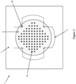
- FIG 2 is a top view of a further example of an LED module according to the present invention.
- the LED module 1 of Figure 2 corresponds to the LED module 1 of Figure 1 , wherein the number and arrangement of the second type LED die 5b and the number of first type LED dies 5a is different compared to Figure 1 .
- the description of the LED module 1 of Figure 1 is correspondingly valid for the LED module 1 of Figure 2 and in the following mainly the difference(s) and optional additional feature(s) of the LED module 1 of Figure 2 are described.
- the number of the first type LED dies 5a shown in Figure 2 is only by way of example and, thus, may be different.
- the number of the second type LED dies 5b shown in Figure 2 is only by way of example and, thus, may be different.
- the first type LED dies 5a may be arranged in the form of a matrix.
- the second type LED dies 5b (e.g. the four second type LED dies 5b as shown in Figure 2 ) may be arranged at the periphery of the opening 4 of the PCB 3, i.e. near the perimeter of the opening 4. This may allow an easier and cheaper manufacturing process for manufacturing the LED module 1.
- the second type LED dies 5b may be symmetrically arranged to each other on the substrate 2.
- wire bonds 6 are exemplarily shown that electrically connect the second type LED dies 5b (by wire bonding) with the PCB 3.
- the shape of the opening 4 of the PCB 3 of the LED module 1 of Figure 2 is circular. This is only by way of example and, thus, the shape may be differently, e.g. it may be elliptic or rectangular.
- FIG 3 is a top view of a further example of an LED module according to the present invention.
- the LED module 1 of Figure 3 is an example of the LED module according to the first aspect of this invention.
- the description of the LED module according to the first aspect of this invention is correspondingly valid for the LED module 1 of Figure 3 .
- the LED module 1 of Figure 3 differs from the LED modules 1 of Figures 1 and 2 in that according to the example of Figure 3 the first type LEDs 5a are surface mounted technology (SMT) first type LEDs, whereas according to the examples of Figures 1 and 2 the first type LEDs 5a are first type LED dies.
- SMT surface mounted technology
- the LED module 1 comprises a substrate 2, a printed circuit board (PCB) 3 arranged on the substrate 2, first type LEDs 5a configured to emit radiation suitable for generating white light, and a second type LED die 5b configured to emit UV-B radiation.
- the PCB 3 comprises an opening 4, and the second type LED die 5b is arranged on the substrate 2 within the opening 4 of the PCB 3.
- the LED module 1 comprises multiple first type LEDs 5a. This is only by way of example and the LED module 1 may comprise a different number of first type LED 5a and the following description is correspondingly valid for the LED module comprising a different number of first type LEDs 5a. That is, the LED module 1 may comprise one or more first type LEDs 5a.
- the LED module 1 comprises one second type LED die 5b. This number is only by way of example and the LED module 1 may comprise more than one second type LED die 5b and the following description is correspondingly valid for an LED module comprising more than one second type LED die 5b.
- the first type LEDs are SMT first type LEDs 5a that are arranged on the PCB 3. That is, the SMT first type LEDs 5a are arranged on the PCB 3, whereas the second type LED die 5b is arranged on the substrate 2 within the opening 4 of the PCB 3.
- the second type LED die 5b is electrically wired by wire bonding, using one or more wire bonds 6 (for example two wire bonds 6, as shown in Figure 3 ), with the PCB 3.
- An matrix material 8 encapsulates the second type LED die 5b and at least partly the one or more wire bonds 6.
- the LED module may comprise a globe top 8 that encapsulates the second type LED die 5b electrically wired with the PCB 3, wherein the globe top is formed by the matrix material 8.
- the matrix material 8 may comprise at least one epoxy and/or at least one silicone.
- the at least one silicone, i.e. the one or more silicones may be for example at least one of silicone rubber(s), and silicone(s) used in flexible UV transmitting lenses.
- the matrix material 8 may comprise one or more resins, such as one or more silicone resins and/or one or more epoxy resins.
- the matrix material 8 may comprise one or more rubbers, such as one or more silicone rubbers and/or one or more epoxy rubbers.
- the aforementioned resin(s) may become due to a heat treatment rubber(s).
- the matrix material 8 may allow UV-B radiation and optionally visible light, e.g. white light, to pass through.
- the matrix material 8 may be transparent or translucent.
- the matrix material 8 may act as a diffusor for the UV-B radiation, optionally for the UV-B radiation and white light.
- the matrix material 8 may be arranged such that it covers the opening 4 of the PCB 3 and optionally a part of the PCB 3.
- the aforementioned part of the PCB 3 may comprise no electric components, e.g. no SMT first type LED 5a.
- the LED module 1 may comprise one or more pads 7 (for example two pads 7, as shown in Figure 3 ) arranged on the PCB 3 for electrically connecting the second type LED die 5b with the PCB 3.
- the second type LED die 5b may be electrically wired by wire bonding, using one or more wire bonds 6, with the one or more pads 7 (in Figure 3 , two wire bonds 6 are exemplarily shown).
- the matrix material 8 may encapsulate or partly encapsulate the one or more pads 7 (not shown in Figure 3 ).
- the matrix material 8 may encapsulate the one or more wire bonds 6 (not shown in Figure 3 ) or partly encapsulate the one or more wire bonds 6 (as shown in Figure 3 ).
- the matrix material 8 may encapsulate the part of the one or more wire bonds 6 that is arranged within the opening 4 of the PCB 3.
- the opening 4 of the PCB 3 may be arranged at a symmetry axis of the PCB. According to the example of Figure 3 , the opening 4 is arranged in the middle of the PCB 3.
- the SMT first type LEDs 5a may be arranged on the PCB 3 around the opening 4 of the PCB 3.
- the SMT first type LEDs 5a may be arranged in the form of a matrix on the PCB 3 around the opening 4 of the PCB 3.
- the number of wire bonds 6 and the number of pads 7 shown in Figure 3 is only by way of example and may be different. The description of Figure 3 is correspondingly valid in case of a different number of wire bonds 6 and/or different number of pads 7 compared to the respective number shown in Figure 3 .
- Figure 4 (A) is a top view of a further example of an LED module according to the present invention
- Figure 4 (B) is a side view of the LED module of Figure 4 (A)
- the LED module 1 of Figures 4 (A) and 4 (B) corresponds to the LED module 1 of Figure 3 , wherein an implementation with regard to the second type LED die 5b is different.
- the description of the LED module 1 of Figure 3 is correspondingly valid for the LED module 1 of Figures 4 (A) and 4 (B) and in the following mainly the difference(s) and optional additional feature(s) of the LED module 1 of Figures 4 (A) and 4 (b) are described.
- the LED module 1 of Figures 4 (A) and 4 (B) comprises a dam 9 that is arranged on the PCB 3 such that the opening 4 of the PCB 3 is arranged within a perimeter of the dam 9.
- the second type LED die 5b is electrically wired with the PCB 3
- an matrix material 10 may be filled inside the perimeter of the dam 9 such that the matrix material 10 covers the second type LED die 5b electrically wired with the PCB 3.
- the dam 9 may be made of one or more resins, such as one or more silicone resins and/or one or more epoxy resins.
- the dam 9 may be made of one or more rubbers, such as one or more silicone rubbers and/or one or more epoxy rubbers.
- the matrix material 10 may comprise one or more resins, such as one or more silicone resins and/or one or more epoxy resins.
- the matrix material 10 may comprise one or more rubbers, such as one or more silicone rubbers and/or one or more epoxy rubbers.
- the matrix material 10 may be as described with regard to the matrix material 8 used in the LED module 1 of Figure 3 .
- the second type LED die 5b may be covered by a dam-and-fill technique using the dam 9 and the matrix material 10.
- the perimeter of the dam 9 equals the perimeter of the opening 4 of the PCB 3 (as exemplarily shown in Figure 4 (A) and 4 (B) ).
- a part of the dam 9 may be arranged inside the opening 4 of the PCB 3 on the substrate 2 (not shown in Figure 4 (A) and 4 (B) ).
- the passage "the dam 9 is arranged on the PCB 3 such that the opening 4 is arranged within a perimeter of the dam 9" means that the rest of the opening 4, on which the part of the dam 9 is not arranged, is arranged within the perimeter of the dam 9.
- the perimeter of the dam 9 may have the shape of the perimeter of the opening 4.
- the perimeter of the dam 9 and the perimeter of the opening 4 have an elliptic shape. This is only by way of example and, thus, the shape may be different, e.g. circular or rectangular.
- the perimeter of the dam 9 may be arranged along the perimeter of the opening 4.
- the matrix material 10 may act as a diffusor for the UV-B radiation, optionally for the UV-B radiation and white light.
- the second type LED die 5b may be electrically wired by wire bonding, using one or more wire bonds 6, with the PCB 3, and the matrix material 10 filled inside the perimeter of the dam 9 covers the second type LED die 5b and the one or more wire bonds 6.
- the matrix material 10 filled inside the perimeter of the dam 9 covers the second type LED die 5b and the part of the one or more wire bonds 6 that is arranged within the opening 4 of the PCB 3.
- the second type LED die 5b may be electrically wired by wire bonding, using the one or more wire bonds 6, with one or more pads 7 arranged on the PCB.
- the one or more pads are arranged on the PCB 3 for electrically connecting the second type LED die 5b with the PCB 3.
- the dam 9 covers at least partly the one or more pads 7.
- the one or more pads 7 for electrically connecting the second type LED die 5b with the PCB 3 may be at least partly arranged at a location where the dam 9 is arranged.
- the one or more pads 7 are partly arranged within the perimeter of the dam 9.
- the perimeter of the dam 9 and the perimeter of the opening 4 are equal and have the same shape so that they may be aligned.
- the perimeter of the dam 9 may be greater than the perimeter of the opening 4 of the PCB 3.
- the dam 9 may be arranged on the PCB 3 such that the dam 9 covers at least partly the one or more pads 7.
- the shape of the perimeter of the opening 4 and the perimeter of the dam 9 may be different.
- the inside surface of the dam 9 may be reflective for UV-B radiation, optionally for UV-B radiation and white light.
- the inside surface of the dam 9 may be white.
- reflective and/or scattering particles may be embedded in the dam 9.
- the inside surface of the dam 9 may comprise reflective and/or scattering particles.
- the aforementioned reflective and/or scattering particles may be configured to reflect and/or scatter UV-B radiation and optionally white light.
- the matrix material 10 may comprise luminescent and/or scattering particles.
- luminescent and/or scattering particles may be embedded into the matrix material 10 filled inside the perimeter of the dam 9.
- the number of wire bonds 6 and the number of pads 7 shown in Figures 4 (A) and 4 (B) is only by way of example and may be different.
- the description of Figures 4 (A) and 4 (B) is correspondingly valid in case of a different number of wire bonds 6 and/or different number of pads 7 compared to the respective number shown in Figures 4 (A) and 4 (B) .
- a lighting system may comprise an LED driver and any LED module of the LED modules of Figures 1 , 2 , 3 , 4 (A) and 4 (B) .
- the LED module is electrically connected to the LED driver and the LED driver is configured to electrically supply the LED module.
- the lighting system may be a luminaire.
- the luminaire may be a down-light luminaire.
- the lighting system may be an LED lamp, such as a retrofit LED lamp.
- the matrix material (e.g. silicone) and/or the conversion layer (fluorescent phosphor) described herein may have a small or negligible absorption of electromagnetic waves at a wavelength of 308 nm.
Landscapes
- Engineering & Computer Science (AREA)
- General Engineering & Computer Science (AREA)
- Led Device Packages (AREA)
Abstract
Description
- The present invention regards an LED module and a lighting system comprising such an LED module, wherein the LED module is configured to emit light having a UV-B component for enhancing human production of vitamin D in the skin. The terms "light" and "visible light" may be used as synonyms. Herein, the term "light emitting diode" is abbreviated by "LED"
- For human health and well-being, it is important that enough vitamin D is available. Vitamin D serves a plurality of purposes in the human body, for example, regulating the absorption of calcium and phosphorus and facilitating normal immune system function, which is extremely important in similar pandemic situations like today. The daily amount of vitamin D needed by a human is estimated to be around 20 µg. Vitamin D is included in a plurality of different food products and can also be supplemented by dietary supplements. Apart from that, the human body is able to produce vitamin D in response to exposing the skin to UV-B radiation. However, the spectrum in which the skin is responsive to UV-B radiation is rather narrow so that even natural sunlight does not provide sufficient UV-B radiation to cause the human body to generate vitamin D during wintertime.
- Nowadays, the problem gets even worse because many people do not spend much time outside in natural sunlight. One reason for that is that people in modern societies rather spend more time indoors maybe even because of the risk of skin cancer, which may be caused by sunlight. Compensating this reduction of a production of vitamin D by dietary supplements requires the people being aware of the fact that their need of vitamin D is higher than what they actually ingest.
- Over the last years, light therapies using dedicated narrowband light sources for quite a number of different diseases became more and more popular. However, a lack of vitamin D is not really a disease in the first place and applying a therapy does not seem suitable to help compensating for a general lack of exposure to sunlight. Such lack of exposure to sunlight is not only a problem for people who do spend most of the time indoors but may also be caused by winter season or longer foggy time periods when the access to natural light is very limited.
- Therefore, it is an object of the present invention to provide an LED module that allows increasing the production of vitamin D by the human body without the need of applying a dedicated therapy or changing the habits, in particular the eating habits.
- This and other objects, which become apparent upon reading the following description, are solved by the subject-matter of the independent claim. The dependent claims refer to preferred embodiments of the invention.
- According to a first aspect of the invention, a light emitting diode module (LED module) is provided. The LED module comprises a substrate, a printed circuit board (PCB) arranged on the substrate, at least one first type LED configured to emit radiation suitable for generating white light, and at least one second type LED die configured to emit UV-B radiation. The PCB comprises an opening, and the at least one second type LED die is arranged on the substrate within the opening of the PCB.
- Since the LED module comprises the at least one first type LED and the at least one second type LED die it is configured to provide UV-B radiation while functioning as a white light source. The UV-B radiation allows increasing vitamin D production. In other words, the entire LED module is configured to emit white light, e.g. for illuminating an area or room, and additionally UV-B radiation. Thus, the LED module is suitable to expose the skin of humans to radiation having a wavelength range that causes an increased vitamin D production. This has the advantage, that in an area where people spend quite a lot of time, and without any need of changing their habits, the production of vitamin D is improved. Thus, the exposure time of the skin of people to UV-B radiation is significantly increased compared to the average exposure times in sunlight only.
- In addition, using at least one second type LED die as the source of UV-B radiation in the LED module is cheaper compared to using one or more LED packages configured to emit UV-B radiation. The material of a package of an LED package configured to emit UV-B radiation is more expensive compared to the material of a package of an LED package for emitting visible light, such as white light. The material of the package of an LED package for emitting UV-B needs to be suitable for the UV-B radiation, i.e. it may not be damaged by the UV-B radiation (e.g. age at a higher aging rate due to the UV-B radiation). Therefore, it is not possible to use simple and cost effective (i.e. cheap) plastic material(s) as are usually used for packaging electric components, such as an LED package for emitting visible light (e.g. white light). The term "packaged LED" may be used as a synonym for the term "LED package". An LED package for emitting radiation, such as UV-B radiation or visible light (e.g. white light), may be understood as an LED unit comprising a package configured for being electrically connected to a PCB, e.g. by soldering or surface mounted technology (SMT). The package packages at least one LED light source for emitting the radiation, such as the UV-B radiation or the visible light (e.g. white light). The terms "to house", "to encase" and "to enclose" may be used as a synonym for the term "to package".
- Therefore, the LED module according to the first aspect allows providing an LED module configured to emit UV-B radiation in addition to light, such as white light, for the same price as an LED module that is merely configured for illumination, i.e. emitting light, such as white light.
- The terms "through opening", "recess" or "cutout" may be used as synonyms for the term "opening". The term "opening of the printed circuit board" is to be understood such that within the opening the PCB is removed, i.e. not present. Thus, the opening is an opening or passage from one surface of the PCB (e.g. the surface in contact with the substrate) to the other surface of the PCB.
- Optionally, the at least one first type LED may comprise one or more blue LED light sources (one or more monochromatic LED light sources) for emitting blue light. The at least one first type LED and/or the LED module may comprise a conversion layer, such as a fluorescent phosphor layer, for converting blue light to light that together with the emitted blue light generates white light. The aforementioned light (that together with blue light generates white light) may for example comprise at least one of the following colors: green, greenish-yellow and yellow. For implementing the aforementioned example of the at least one first type LED any conversion layer that is known may be used.. Optionally, the at least one first type LED may be configured to emit light of two or more different colors for emitting white light. The at least one first type LED and/or the LED module may comprise a layer, such as a diffuser layer, for mixing the light of two or more different colors to generate white light. For implementing the aforementioned second example of the at least one first type LED any layer for mixing light of two or more different colors to generate white light that is known may be used.
- The term "chip" may be used as a synonym for the term "die". Both terms refer to an unpackaged element. That is, an LED die or LED chip may be understood as an unpackaged LED unit, i.e. an LED unit without a package.
- The at least one second type LED die may be configured to emit electromagnetic waves with a wavelength between 280 nm and 350 nm. Optionally, the at least one second type LED die is configured to emit UV-B radiation with a peak wavelength in a range between 300 and 320 nm, e.g. with a peak wavelength of 308 nm. The at least one second type LED die may for example be adhered or soldered to the substrate. The at least one second type LED die may be arranged on the substrate such that it may be wire bonded, using one or more wire bonds, to the PCB, e.g. to one or more pads of the PCB, for electrically connecting the at least one second type LED die with the PCB. The wire bonding may be performed by gold wire bonding. Thus, the wire bonds may be gold wire bonds. In case the LED module comprises multiple second type LED dies, the second type LED dies may be arranged in the form of a matrix on the substrate.
- Optionally, the at least one second type LED die may be arranged in the middle of the opening. In this case, compared to a case where the at least one second type LED is arranged near the border (i.e. perimeter) of the opening of the PCB, less UV-B radiation is present at the border of the opening and, thus, less UV-B radiation reaches the PCB. Therefore, an aging effect of the PCB due to the UV-B radiation may be reduced. Anyway, the UV-B radiation of the at least one second type LED die in a lateral (i.e. sideways) direction may be small, because the UV-B radiation of the at least one second type LED die may be mainly in axial direction, i.e. perpendicular to the at least one second type LED die.
- Optionally, the at least one second type LED die may be peripherally arranged on the substrate, i.e. near the border of the opening. Since the UV-B radiation of the at least one second type LED die in a lateral (i.e. sideways) direction may be small, because the UV-B radiation of the at least one second type LED die may be mainly in axial direction (i.e. perpendicular to the at least one second type LED die), an aging effect of the PCB due to the UV-B radiation may be acceptable or negligible. For example the PCB may comprise or be covered by a material that is suited for UV-B radiation, e.g. durable with respect to aging due to UV-B radiation. Arranging the at least one second type LED die peripherally may allow an easier and cheaper manufacturing process for manufacturing the LED module.
- The LED module may comprise one or more connectors for being electrically connected directly to an LED module driver, e.g. ballast, that is configured to drive the LED module, e.g. provide electrical supply for the LED module in order to drive the LED light sources of the LED module to emit light. The term "LED driver" may be used as a synonym for the term "LED module driver".
- The substrate may be a metal substrate, such as an aluminum substrate. It is a heat sink of the LED module. In addition or alternatively, the substrate may be made of any other known material(s) suitable for providing a heat sink. The PCB may comprise a matrix material and electrical wiring, e.g. copper wiring, on the matrix material. In case the matrix material encapsulates something, it may be referred to as "encapsulating matrix material". In case the matrix material is filling something, it may be referred to as "filler matrix material". The matrix material may be an FR-4 material. In other words, the PCB may be an FR-4 PCB. The matrix material may comprise epoxy material and/or composite material. The present invention is not limited to a specific PCB and, thus, the PCB may be made of any material known for implementing a PCB. The PCB layer on the substrate may be referred to as "laminate". The terms "epoxy" and "epoxy material" may be used as synonyms. Optionally, the substrate may be a metal substrate (e.g. aluminum substrate) and the PCB may be an FR-4 PCB.
- Optionally, the at least one first type LED is at least one first type LED die that is arranged on the substrate within the opening of the PCB.
- For example, the at least one first type LED die may be at least one blue LED die (monochromatic LED die) for emitting blue light. A conversion layer, such as a fluorescent phosphor layer, may cover the at least one blue LED die for converting the blue light to light that together with the emitted blue light generates white light. The aforementioned light may for example comprise at least one of the following colors: green, greenish-yellow and yellow. Any conversion layer that is known may be used. The conversion layer may cover the at least one blue LED die and the at least one second type LED die. Optionally, the conversion layer may cover the opening of the PCB.
- Optionally, the at least one first type LED die may be any other known monochromatic LED die configured to emit light that may be converted by any known conversion layer to white light. The above description with regard to the blue LED die and the conversion layer for generating white light is correspondingly valid. Any known LED die configured to emit radiation suitable for generating white light may be used as the at least one first type LED die.
- The at least one first type LED die may be arranged on the substrate such that it may be wire bonded, using one or more wire bonds, to the PCB, e.g. to one or more pads of the PCB, for electrically connecting the at least one first type LED die with the PCB. The wire bonding may be performed by gold wire bonding. Thus, the wire bonds may be gold wire bonds. The description with regard to the at least one second type LED die may be correspondingly valid for the at least one first type LED die and vice versa.
- In case the LED module comprises multiple first type LED dies, the first type LED dies may be arranged in the form of a matrix on the substrate.
- Optionally, the at least one first type LED may be peripherally arranged on the substrate, i.e. near the border of the opening. The at least first type LED die may be peripherally arranged on the substrate and the at least one second type LED die may be arranged on the substrate in the middle of the opening. For example, in case the LED module comprises multiple first type LED dies, the at least one second type LED die may be arranged on the substrate in the middle of the opening and the first type LED dies may be arranged on the substrate around the at least one second type LED die, optionally in the form of a matrix. Optionally, in case the LED module comprises multiple first type LED dies, the first type LED dies may be arranged on the substrate in the middle of the opening, optionally in the form of a matrix; wherein the at least one second type LED die may be peripherally arranged. For example, when the LED module comprises multiple second type LED dies in the aforementioned optional case, the second type LED dies may be symmetrically arranged to each other near the border of the opening.
- Optionally, the at least one first type LED is at least one surface mounted technology first type LED (SMT first type LED) that is arranged on the PCB.
- The term "surface mounted device (SMD) first type LED" may be used as a synonym for the term "SMT first type LED". The SMT first type LED comprises a package configured for being electrically connected to the PCB by SMT, i.e. being surface mounted on the PCB for electrical connection with the PCB. The package packages at least one LED light source for emitting radiation suitable for generating white light.
- Optionally, the at least one SMT first type LED may comprise at least one monochromatic LED light source (e.g. at least one blue LED light source) and a conversion layer (e.g. a fluorescent phosphor layer) for converting the light emitted by the at least one monochromatic LED light to light that together with the emitted light (emitted by the at least one monochromatic LED light) generates white light. Optionally, the at least one SMT first type LED may comprise two or more LED light sources (e.g. two or more monochromatic LED light sources) for emitting light of two or more different colors and a layer, such as a diffuser layer, for mixing the light of the two or more different colors to generate white light. The at least one SMT first type LED may be configured to emit white light. Any known SMT LED configured to emit white light or radiation suitable for generating white light may be used as the at least one SMT first type LED.
- The use of at least one SMT first type LED as the at least one first type LED allows not using a conversion layer, such as a fluorescent phosphor layer, in the area of the opening of the PCB, where the at least one second type LED die is arranged on the substrate. As a result the efficiency of the UV-B radiation emitted by the at least one second type LED die may be increased, because there is no such conversion layer that would cause absorption of the UV-B radiation. Nevertheless, the absorption of the UV-B radiation by such conversion layer is small enough that covering the at least one second type LED die or the opening with such conversion layer still allows a UV-B radiation sufficient for achieving the above described positive effects, e.g. sufficient for enhancing Vitamin D production in a human body.
- Optionally, the at least one first type LED is at least one first type LED die arranged on the substrate within the opening of the PCB, and at least one SMT first type LED, which is configured to emit radiation suitable for generating white light, is arranged on the PCB. The description with regard to the at least one first type LED being at least one SMT first type LED may be correspondingly valid for the aforementioned at least one SMT first type LED.
- Optionally, the at least one first type LED is at least one SMT first type LED arranged on the PCB, and at least one first type LED die, which is configured to emit radiation suitable for generating white light, is arranged on the substrate within the opening of the PCB. The description with regard to the at least one first type LED being at least one first type LED die may be correspondingly valid for the aforementioned at least one first type LED die.
- Optionally, the at least one second type LED die is electrically wired with the PCB, and an matrix material encapsulates the at least one second type LED die electrically wired with the PCB.
- Since the matrix material encapsulates the at least one second type LED die it allows the UV-B radiation emitted by the at least one second type LED die to pass through. In other words, the matrix material negligibly absorbs the UV-B radiation. The matrix material may comprise one or more silicone(s), e.g. silicone rubber(s), and/or silicone(s) used in flexible UV transmitting lenses. The term "silicone material(s)" may be used as a synonym for the term "silicone(s)".
- In case the at least one first type LED is the at least one first type LED die, the at least one second type LED die and the at least one first type LED die may be electrically wired with the PCB. The matrix material may encapsulate the at least one second type LED die and the at least one first type LED die electrically wired with the PCB.
- Since the matrix material encapsulates the at least one second type LED die and the at least one first type LED die it allows the UV-B radiation emitted by the at least one second type LED die and visible light (e.g. white light) to pass through. In other words, the matrix material negligibly absorbs the UV-B radiation and visible light. The matrix material may comprise one or more silicone(s), e.g. silicone rubber(s), and/or silicone(s) used in flexible UV transmitting lenses. Optionally, the matrix material encapsulates a conversion layer (e.g. a fluorescent phosphor layer) for converting light (e.g. blue light) emitted by the at least one first type LED die (e.g. being at least one blue LED die for emitting blue light) to light that together with the emitted light (e.g. blue light) generates white light. Optionally, the matrix material may comprise a conversion material (e.g. fluorescent phosphor) for converting light (e.g. blue light) emitted by the at least one first type LED die (e.g. being at least one blue LED die for emitting blue light) to light that together with the emitted light (e.g. blue light) generates white light.
- The encapsulating matrix material may be referred to by the term "globe top". In other words, the LED module may comprise a globe top that encapsulates the at least one second type LED die and optionally the optional at least one first type LED die electrically wired with the PCB, wherein the globe top is formed by the matrix material. The at least one second type LED die and optionally the optional at least one first type LED die may be electrically wired by wire bonding with the PCB. The matrix material may comprise at least one epoxy and/or at least one silicone. For example, the matrix material may comprise one or more resins, such as one or more silicone resins and/or one or more epoxy resins. The matrix material may comprise one or more rubbers, such as one or more silicone rubbers and/or one or more epoxy rubbers. The aforementioned resin(s) may become due to a heat treatment rubber(s). The matrix material may allow UV-B radiation and optionally visible light, e.g. white light, to pass through. The matrix material may be transparent or translucent. The matrix material may act as a diffusor for the UV-B radiation, optionally for the UV-B radiation and white light.
- Optionally, the at least one second type LED die is electrically wired by wire bonding, using one or more wire bonds, with the PCB, and the matrix material encapsulates the at least one second type LED die and at least partly the one or more wire bonds.
- The LED module may comprise one or more pads arranged on the PCB for electrically connecting the at least one second type LED die with the PCB. The at least one second type LED die may be electrically wired by wire bonding with the one or more pads. The matrix material may encapsulate or partly encapsulate the one or more pads. The matrix material may encapsulate the one or more wire bonds or partly encapsulate the one or more wire bonds. The matrix material may encapsulate the part of the one or more wire bonds that is arranged within the opening.
- Optionally, the at least one first type LED die is electrically wired by wire bonding, using one or more wire bonds, with the PCB, and the matrix material encapsulates the at least one first type LED die and at least partly the one or more wire bonds.
- The LED module may comprise one or more pads arranged on the PCB for electrically connecting the at least one first type LED die with the PCB. The at least one first type LED die may be electrically wired by wire bonding with the one or more pads. The matrix material may encapsulate or partly encapsulate the one or more pads. The matrix material may encapsulate the one or more wire bonds or partly encapsulate the one or more wire bonds. The matrix material may encapsulate the part of the one or more wire bonds that is arranged within the opening.
- Optionally, a dam is arranged on the PCB such that the opening is arranged within a perimeter of the dam. The at least one second type LED die may be electrically wired with the PCB, and an matrix material may be filled inside the perimeter of the dam such that the matrix material covers the at least one second type LED die electrically wired with the PCB.
- The dam may be made of one or more resins, such as one or more silicone resins and/or one or more epoxy resins. For example, the dam may be made of one or more rubbers, such as one or more silicone rubbers and/or one or more epoxy rubbers. The aforementioned resin(s) may become due to a heat treatment rubber(s). The matrix material filled inside the perimeter of the dam may comprise luminescent and/or scattering particles. For examples, luminescent and/or scattering particles may be embedded into the matrix material filled inside the perimeter of the dam.
- Since the matrix material covers the at least one second type LED die it allows the UV-B radiation emitted by the at least one second type LED die to pass through. In other words, the matrix material negligibly absorbs the UV-B radiation. The matrix material may comprise one or more silicone(s), e.g. silicone rubber(s), and/or silicone(s) used in flexible UV transmitting lenses.
- In case the at least one first type LED is the at least one first type LED die, a dam is optionally arranged on the PCB such that the opening is arranged within a perimeter of the dam. The at least one second type LED die and the at least one first type LED die may be electrically wired with the PCB. The matrix material may be filled inside the perimeter of the dam such that the matrix material covers the at least one second type LED die and the at least one first type LED die electrically wired with the PCB.
- Since the matrix material covers the at least one second type LED die and the at least one first type LED die it allows the UV-B radiation emitted by the at least one second type LED die and visible light (e.g. white light) to pass through. In other words, the matrix material negligibly absorbs the UV-B radiation and visible light. The matrix material may comprise one or more silicone(s), e.g. silicone rubber(s), and/or silicone(s) used in flexible UV transmitting lenses. Optionally, the matrix material covers a conversion layer (e.g. a fluorescent phosphor layer) for converting light (e.g. blue light) emitted by the at least one first type LED die (e.g. being at least one blue LED die for emitting blue light) to light that together with the emitted light (e.g. blue light) generates white light. Optionally, the matrix material may comprise a conversion material (e.g. fluorescent phosphor) for converting light (e.g. blue light) emitted by the at least one first type LED die (e.g. being at least one blue LED die for emitting blue light) to light that together with the emitted light (e.g. blue light) generates white light.
- In other words the at least one second type LED die and optionally the optional at least one first type LED die may be enclosed by a dam-and-fill technique using a matrix material. The matrix material may comprise at least one epoxy and/or at least one silicone. For example, the matrix material may comprise one or more resins, such as one or more silicone resins and/or one or more epoxy resins. The matrix material may comprise one or more rubbers, such as one or more silicone rubbers and/or one or more epoxy rubbers. The aforementioned resin(s) may become due to a heat treatment rubber(s). The matrix material may allow UV-B radiation and optionally visible light, e.g. white light, to pass through. The matrix material may be transparent or translucent.
- Optionally, the perimeter of the dam equals the perimeter of the opening. The perimeter of the dam may have the shape of the perimeter of the opening. That is the perimeter of the dam may be arranged along the perimeter of the opening. The matrix material may act as a diffusor for the UV-B radiation, optionally for the UV-B radiation and white light. Optionally, a part of the dam may be arranged inside the opening on the substrate. In this case, the passage "the dam is arranged on the PCB such that the opening is arranged within a perimeter of the dam" means that the rest of the opening, on which the part of the dam is not arranged, is arranged within the perimeter of the dam.
- Optionally, the at least one second type LED die is electrically wired by wire bonding, using one or more wire bonds, with the PCB, and the matrix material filled inside the perimeter of the dam covers the at least one second type LED die and the one or more wire bonds.
- For example, the matrix material filled inside the perimeter of the dam covers the at least one second type LED die and the part of the one or more wire bonds that is arranged within the opening of the PCB.
- Optionally, the at least one second type LED die is electrically wired by wire bonding, using the one or more wire bonds, with one or more pads arranged on the PCB, and the dam covers at least partly the one or more pads.
- In other words, the one or more pads for electrically connecting the at least one second type LED die with the PCB may be at least partly arranged at a location where the dam is arranged. Optionally, the one or more pads are partly arranged within the perimeter of the dam. Optionally, the perimeter of the dam is greater than the perimeter of the opening such that the dam covers at least partly the one or more pads. Optionally, the perimeter of the dam is greater than the perimeter of the opening. The perimeter of the dam may have the shape of the perimeter of the opening.
- Optionally, the at least one first type LED die is electrically wired by wire bonding, using one or more wire bonds, with the PCB, and the matrix material filled inside the perimeter of the dam covers the at least one first type LED die and the one or more wire bonds.
- For example, the matrix material filled inside the perimeter of the dam covers the at least one first type LED die and the part of the one or more wire bonds that is arranged within the opening of the PCB.
- Optionally, the at least one first type LED die is electrically wired by wire bonding, using the one or more wire bonds, with one or more pads arranged on the PCB, and the dam covers at least partly the one or more pads.
- In other words, the one or more pads for electrically connecting the at least one first type LED die with the PCB may be at least partly arranged at a location where the dam is arranged. Optionally, the one or more pads are partly arranged within the perimeter of the dam. Optionally, the perimeter of the dam is greater than the perimeter of the opening such that the dam covers at least partly the one or more pads.
- Optionally, the inside surface of the dam is reflective for UV-B radiation. The inside surface of the dam may be reflective for UV-B radiation and white light.
- For example, the inside surface of the dam may be white. In addition or alternatively, reflective and/or scattering particles may be embedded in the dam. For example, the inside surface of the dam may comprise reflective and/or scattering particles. The aforementioned reflective and/or scattering particles may be configured to reflect and/or scatter UV-B radiation and optionally white light.
- Optionally, the opening is arranged at a symmetry axis of the PCB, optionally in the middle of the PCB.
- The opening may have a circular, elliptic or a rectangular shape.
- In order to achieve the LED module according to the first aspect of the present invention, some or all of the above-described optional features may be combined with each other.
- According to a second aspect of the invention, a lighting system is provided. The lighting system comprises an LED driver, and an LED module according to the first aspect, as described above, that is electrically connected to the LED driver. The LED driver is configured to electrically supply the LED module.
- The lighting system may be a luminaire. The lighting system may be an LED lamp, such as a retrofit LED lamp. The term "illuminant" may be used as a synonym for the term "lamp". A retrofit LED lamp may be understood as an LED light source that has the form and electrical connection of a classical lamp, such as a light bulb, halogen bulb etc., usable in classical luminaires. The luminaire may be a down-light luminaire.
- The above description with regard to the LED module according to the first aspect of the present invention is also valid for the lighting system according to the second aspect.
- The lighting system according to the second aspect achieves the same advantages as the LED module according to the first aspect.
- All steps which are performed by the various entities described in the present application as well as the functionalities described to be performed by the various entities are intended to mean that the respective entity is adapted to or configured to perform the respective steps and functionalities.
- In the following, the invention is described exemplarily with reference to the enclosed Figures, in which
- Figure 1
- is a cross-sectional view of an example of an LED module according to the present invention;
- Figure 2
- is a top view of a further example of an LED module according to the present invention;
- Figure 3
- is a top view of a further example of an LED module according to the present invention;
- Figure 4 (A)
- is a top view of a further example of an LED module according to the present invention; and
- Figure 4 (B)
- is a side view of the LED module of
Figure 4 (A) . - In the Figures, corresponding elements have the same reference signs. The proportions and dimensions of the elements shown in the Figures do not represent the LED module to scale, but are merely chosen to describe the structure and function of the LED module.
-
Figure 1 is a cross-sectional view of an example of an LED module according to the present invention. TheLED module 1 ofFigure 1 is an example of the LED module according to the first aspect of this invention. The description of the LED module according to the first aspect of this invention is correspondingly valid for theLED module 1 ofFigure 1 . - As shown in
Figure 1 , theLED module 1 comprises asubstrate 2, a printed circuit board (PCB) 3 arranged on thesubstrate 2,first type LEDs 5a configured to emit radiation suitable for generating white light, and a secondtype LED die 5b configured to emit UV-B radiation. ThePCB 3 comprises anopening 4, and the secondtype LED die 5b is arranged on thesubstrate 2 within theopening 4 of thePCB 3. According toFigure 1 , theLED module 1 comprises twelvefirst type LEDs 5a. This is only by way of example and theLED module 1 may comprise a different number offirst type LED 5a and the following description is correspondingly valid for the LED module comprising a different number offirst type LEDs 5a. That is, theLED module 1 may comprise one or morefirst type LEDs 5a. The terms "one or more" and "at least one" may be used as synonyms. According toFigure 1 , theLED module 1 comprises one secondtype LED die 5b. This number is only by way of example and theLED module 1 may comprise more than one secondtype LED die 5b and the following description is correspondingly valid for an LED module comprising more than one secondtype LED die 5b. - According to the example of
Figure 1 , the first type LEDs are first type LED dies 5a that are arranged on thesubstrate 2 within theopening 4 of thePCB 3. That is, the first type LED dies 5a and the secondtype LED die 5b are together arranged on thesubstrate 2 within theopening 4 of thePCB 3. - For example, the first type LED dies 5a are blue LED dies for emitting blue light and the
LED module 1 comprises a conversion layer (not shown inFigure 1 ), such as a fluorescent phosphor layer, that covers the blue LED dies 5a for converting the blue light (emitted by the blue LED dies 5a) to light that together with the emitted blue light generates white light. The conversion layer may also cover the secondtype LED die 5b. Optionally, the first type LED dies 5a may be any other known monochromatic LED dies configured to emit light that may be converted by any known conversion layer to white light and the conversion layer is configured to convert the light emitted by the monochromatic LED dies to white light. The conversion layer may cover theopening 4 of thePCB 3. - In addition or alternatively, the first type LED dies 5a and the second
type LED die 5b may be covered by an matrix material (not shown inFigure 1 ) allowing visible light and the UV-B radiation to pass through. The matrix material may cover theopening 4 of thePCB 3. The matrix material may be at least one epoxy and/or at least one silicone. The at least one silicone, i.e. the one or more silicones, may be for example at least one of silicone rubber(s), and silicone(s) used in flexible UV transmitting lenses. For example, the matrix material may comprise one or more resins, such as one or more silicone resins and/or one or more epoxy resins. The matrix material may comprise one or more rubbers, such as one or more silicone rubbers and/or one or more epoxy rubbers. The aforementioned resin(s) may become due to a heat treatment rubber(s). - The matrix material may be arranged as outlined with regard to
Figure 3 orFigures 4 (A) and4 (B) . That is, the matrix material may encapsulate the first type LED dies 5a and the secondtype LED die 5b. The encapsulating matrix material may be referred to by the term "globe top". In other words, the LED module may comprise a globe top that encapsulates the first type LED dies 5a and the secondtype LED die 5a, wherein the globe top is formed by the matrix material. Alternatively, the LED module may comprise a dam (not shown inFigure 1 ) that is arranged on thePCB 3 such that theopening 4 is within the perimeter of the dam; and the matrix material is filled inside the perimeter of the dam such that the matrix material covers the first type LED dies 5a and the secondtype LED die 5b. The dam and/or the matrix material may comprise one or more resins, such as one or more silicone resins and/or one or more epoxy resins. For example, the dam and/or the matrix material may comprise one or more rubbers, such as one or more silicone rubbers and/or one or more epoxy rubbers. The aforementioned resin(s) may become due to a heat treatment rubber(s). - The first type LED dies 5a and the second
type LED die 5b may be wire bonded, using wire bonds, with thePCB 3, e.g. with pads arranged on thePCB 3 for connecting the respective LED die with the PCB 3 (not shown inFigure 1 ). The matrix material may encapsulate or cover at least partly the wire bonds. For example, the matrix material may encapsulate or cover the part of the wire bonds arranged within theopening 4. This allows preventing any mechanical damage to the bond wires and ensuring that the wire bonds and the substrate 2 (e.g. being an aluminum substrate) are not in contact or do not come into contact. - As shown in
Figure 1 , the secondtype LED die 5b may be arranged in the middle of theopening 4 of thePCB 3. This may reduce an aging effect of thePCB 3 due to the UV-B radiation emitted by the secondtype LED die 5b, as outlined above. - For further details on the
LED module 1 ofFigure 1 reference is made to the description of the LED module according to the first aspect of the invention. -
Figure 2 is a top view of a further example of an LED module according to the present invention. TheLED module 1 ofFigure 2 corresponds to theLED module 1 ofFigure 1 , wherein the number and arrangement of the secondtype LED die 5b and the number of first type LED dies 5a is different compared toFigure 1 . Thus, the description of theLED module 1 ofFigure 1 is correspondingly valid for theLED module 1 ofFigure 2 and in the following mainly the difference(s) and optional additional feature(s) of theLED module 1 ofFigure 2 are described. The number of the first type LED dies 5a shown inFigure 2 is only by way of example and, thus, may be different. The number of the second type LED dies 5b shown inFigure 2 is only by way of example and, thus, may be different. - As shown in
Figure 2 , the first type LED dies 5a may be arranged in the form of a matrix. The second type LED dies 5b (e.g. the four second type LED dies 5b as shown inFigure 2 ) may be arranged at the periphery of theopening 4 of thePCB 3, i.e. near the perimeter of theopening 4. This may allow an easier and cheaper manufacturing process for manufacturing theLED module 1. The second type LED dies 5b may be symmetrically arranged to each other on thesubstrate 2. - In
Figure 2 wire bonds 6 are exemplarily shown that electrically connect the second type LED dies 5b (by wire bonding) with thePCB 3. The shape of theopening 4 of thePCB 3 of theLED module 1 ofFigure 2 is circular. This is only by way of example and, thus, the shape may be differently, e.g. it may be elliptic or rectangular. - For further details on the
LED module 1 ofFigure 2 reference is made to the description of the LED module according to the first aspect of the invention and theLED module 1 ofFigure 1 . -
Figure 3 is a top view of a further example of an LED module according to the present invention. TheLED module 1 ofFigure 3 is an example of the LED module according to the first aspect of this invention. The description of the LED module according to the first aspect of this invention is correspondingly valid for theLED module 1 ofFigure 3 . TheLED module 1 ofFigure 3 differs from theLED modules 1 ofFigures 1 and2 in that according to the example ofFigure 3 thefirst type LEDs 5a are surface mounted technology (SMT) first type LEDs, whereas according to the examples ofFigures 1 and2 thefirst type LEDs 5a are first type LED dies. - As shown in
Figure 3 , theLED module 1 comprises asubstrate 2, a printed circuit board (PCB) 3 arranged on thesubstrate 2,first type LEDs 5a configured to emit radiation suitable for generating white light, and a secondtype LED die 5b configured to emit UV-B radiation. ThePCB 3 comprises anopening 4, and the secondtype LED die 5b is arranged on thesubstrate 2 within theopening 4 of thePCB 3. According toFigure 1 , theLED module 1 comprises multiplefirst type LEDs 5a. This is only by way of example and theLED module 1 may comprise a different number offirst type LED 5a and the following description is correspondingly valid for the LED module comprising a different number offirst type LEDs 5a. That is, theLED module 1 may comprise one or morefirst type LEDs 5a. According toFigure 1 , theLED module 1 comprises one secondtype LED die 5b. This number is only by way of example and theLED module 1 may comprise more than one secondtype LED die 5b and the following description is correspondingly valid for an LED module comprising more than one secondtype LED die 5b. - According to the example of
Figure 3 , the first type LEDs are SMTfirst type LEDs 5a that are arranged on thePCB 3. That is, the SMTfirst type LEDs 5a are arranged on thePCB 3, whereas the secondtype LED die 5b is arranged on thesubstrate 2 within theopening 4 of thePCB 3. - As shown in
Figure 3 , the secondtype LED die 5b is electrically wired by wire bonding, using one or more wire bonds 6 (for example twowire bonds 6, as shown inFigure 3 ), with thePCB 3. Anmatrix material 8 encapsulates the secondtype LED die 5b and at least partly the one ormore wire bonds 6. In other words, the LED module may comprise aglobe top 8 that encapsulates the second type LED die 5b electrically wired with thePCB 3, wherein the globe top is formed by thematrix material 8. Thematrix material 8 may comprise at least one epoxy and/or at least one silicone. The at least one silicone, i.e. the one or more silicones, may be for example at least one of silicone rubber(s), and silicone(s) used in flexible UV transmitting lenses. For example, thematrix material 8 may comprise one or more resins, such as one or more silicone resins and/or one or more epoxy resins. Thematrix material 8 may comprise one or more rubbers, such as one or more silicone rubbers and/or one or more epoxy rubbers. The aforementioned resin(s) may become due to a heat treatment rubber(s). Thematrix material 8 may allow UV-B radiation and optionally visible light, e.g. white light, to pass through. Thematrix material 8 may be transparent or translucent. Thematrix material 8 may act as a diffusor for the UV-B radiation, optionally for the UV-B radiation and white light. Thematrix material 8 may be arranged such that it covers theopening 4 of thePCB 3 and optionally a part of thePCB 3. The aforementioned part of thePCB 3 may comprise no electric components, e.g. no SMTfirst type LED 5a. - As indicated in
Figure 3 , theLED module 1 may comprise one or more pads 7 (for example twopads 7, as shown inFigure 3 ) arranged on thePCB 3 for electrically connecting the secondtype LED die 5b with thePCB 3. The secondtype LED die 5b may be electrically wired by wire bonding, using one ormore wire bonds 6, with the one or more pads 7 (inFigure 3 , twowire bonds 6 are exemplarily shown). Thematrix material 8 may encapsulate or partly encapsulate the one or more pads 7 (not shown inFigure 3 ). Thematrix material 8 may encapsulate the one or more wire bonds 6 (not shown inFigure 3 ) or partly encapsulate the one or more wire bonds 6 (as shown inFigure 3 ). Thematrix material 8 may encapsulate the part of the one ormore wire bonds 6 that is arranged within theopening 4 of thePCB 3. - As shown in
Figure 3 , theopening 4 of thePCB 3 may be arranged at a symmetry axis of the PCB. According to the example ofFigure 3 , theopening 4 is arranged in the middle of thePCB 3. The SMTfirst type LEDs 5a may be arranged on thePCB 3 around theopening 4 of thePCB 3. For example, as shown inFigure 3 , the SMTfirst type LEDs 5a may be arranged in the form of a matrix on thePCB 3 around theopening 4 of thePCB 3. - The description with regard to using the
globe top 8 for encapsulating or covering the secondtype LED die 5b of theLED module 1 ofFigure 3 may be correspondingly true for describing an optional way of encapsulating or covering the at least one secondtype LED die 5b and optionally the first type LED dies 5a of theLED module 1 ofFigure 1 orFigure 2 . - The number of
wire bonds 6 and the number ofpads 7 shown inFigure 3 is only by way of example and may be different. The description ofFigure 3 is correspondingly valid in case of a different number ofwire bonds 6 and/or different number ofpads 7 compared to the respective number shown inFigure 3 . - For further details on the
LED module 1 ofFigure 3 reference is made to the description of the LED module according to the first aspect of the invention. -
Figure 4 (A) is a top view of a further example of an LED module according to the present invention; andFigure 4 (B) is a side view of the LED module ofFigure 4 (A) . TheLED module 1 ofFigures 4 (A) and 4 (B) corresponds to theLED module 1 ofFigure 3 , wherein an implementation with regard to the secondtype LED die 5b is different. Thus, the description of theLED module 1 ofFigure 3 is correspondingly valid for theLED module 1 ofFigures 4 (A) and 4 (B) and in the following mainly the difference(s) and optional additional feature(s) of theLED module 1 ofFigures 4 (A) and 4 (b) are described. - Instead of using a
globe top 8 for encapsulating or covering the secondtype LED die 5b (as is done in the example ofFigure 3 ), theLED module 1 ofFigures 4 (A) and 4 (B) comprises adam 9 that is arranged on thePCB 3 such that theopening 4 of thePCB 3 is arranged within a perimeter of thedam 9. As shown inFigures 4 (A) and 4 (B) , the secondtype LED die 5b is electrically wired with thePCB 3, and anmatrix material 10 may be filled inside the perimeter of thedam 9 such that thematrix material 10 covers the second type LED die 5b electrically wired with thePCB 3. Thedam 9 may be made of one or more resins, such as one or more silicone resins and/or one or more epoxy resins. Optionally, thedam 9 may be made of one or more rubbers, such as one or more silicone rubbers and/or one or more epoxy rubbers. Thematrix material 10 may comprise one or more resins, such as one or more silicone resins and/or one or more epoxy resins. Optionally, thematrix material 10 may comprise one or more rubbers, such as one or more silicone rubbers and/or one or more epoxy rubbers. - The
matrix material 10 may be as described with regard to thematrix material 8 used in theLED module 1 ofFigure 3 . - In other words, according to
Figures 4 (A) and 4 (b) , the secondtype LED die 5b may be covered by a dam-and-fill technique using thedam 9 and thematrix material 10. - Optionally, the perimeter of the
dam 9 equals the perimeter of theopening 4 of the PCB 3 (as exemplarily shown inFigure 4 (A) and 4 (B) ). Optionally, a part of thedam 9 may be arranged inside theopening 4 of thePCB 3 on the substrate 2 (not shown inFigure 4 (A) and 4 (B) ). In this case, the passage "thedam 9 is arranged on thePCB 3 such that theopening 4 is arranged within a perimeter of thedam 9" means that the rest of theopening 4, on which the part of thedam 9 is not arranged, is arranged within the perimeter of thedam 9. The perimeter of thedam 9 may have the shape of the perimeter of theopening 4. According toFigure 4 (A) , the perimeter of thedam 9 and the perimeter of theopening 4 have an elliptic shape. This is only by way of example and, thus, the shape may be different, e.g. circular or rectangular. The perimeter of thedam 9 may be arranged along the perimeter of theopening 4. Thematrix material 10 may act as a diffusor for the UV-B radiation, optionally for the UV-B radiation and white light. - As shown in
Figures 4 (A) and 4 (B) , the secondtype LED die 5b may be electrically wired by wire bonding, using one ormore wire bonds 6, with thePCB 3, and thematrix material 10 filled inside the perimeter of thedam 9 covers the secondtype LED die 5b and the one ormore wire bonds 6. For example, thematrix material 10 filled inside the perimeter of thedam 9 covers the secondtype LED die 5b and the part of the one ormore wire bonds 6 that is arranged within theopening 4 of thePCB 3. - As shown in
Figures 4 (A) and 4 (B) , the secondtype LED die 5b may be electrically wired by wire bonding, using the one ormore wire bonds 6, with one ormore pads 7 arranged on the PCB. The one or more pads are arranged on thePCB 3 for electrically connecting the secondtype LED die 5b with thePCB 3. Thedam 9 covers at least partly the one ormore pads 7. In other words, the one ormore pads 7 for electrically connecting the secondtype LED die 5b with thePCB 3 may be at least partly arranged at a location where thedam 9 is arranged. Optionally, the one ormore pads 7 are partly arranged within the perimeter of thedam 9. - According to the example of
Figures 4 (A) and 4 (B) , the perimeter of thedam 9 and the perimeter of theopening 4 are equal and have the same shape so that they may be aligned. Alternatively, the perimeter of thedam 9 may be greater than the perimeter of theopening 4 of thePCB 3. In this case, thedam 9 may be arranged on thePCB 3 such that thedam 9 covers at least partly the one ormore pads 7. The shape of the perimeter of theopening 4 and the perimeter of thedam 9 may be different. - The inside surface of the
dam 9 may be reflective for UV-B radiation, optionally for UV-B radiation and white light. For example, the inside surface of thedam 9 may be white. In addition or alternatively, reflective and/or scattering particles may be embedded in thedam 9. For example, the inside surface of thedam 9 may comprise reflective and/or scattering particles. The aforementioned reflective and/or scattering particles may be configured to reflect and/or scatter UV-B radiation and optionally white light. Thematrix material 10 may comprise luminescent and/or scattering particles. For examples, luminescent and/or scattering particles may be embedded into thematrix material 10 filled inside the perimeter of thedam 9. - The description with regard to using the dam-and-fill technique for covering the second
type LED die 5b of theLED module 1 ofFigures 4 (A) and 4(B) may be correspondingly true for describing an optional way of covering the at least one secondtype LED die 5b and optionally the first type LED dies 5a of theLED module 1 ofFigure 1 orFigure 2 . - The number of
wire bonds 6 and the number ofpads 7 shown inFigures 4 (A) and 4 (B) is only by way of example and may be different. The description ofFigures 4 (A) and 4 (B) is correspondingly valid in case of a different number ofwire bonds 6 and/or different number ofpads 7 compared to the respective number shown inFigures 4 (A) and 4 (B) . - For further details on the
LED module 1 ofFigure 4 (A) and 4 (B) reference is made to the description of the LED module according to the first aspect of the invention and theLED module 1 ofFigure 3 . - According to examples of the present invention, a lighting system may comprise an LED driver and any LED module of the LED modules of
Figures 1 ,2 ,3 ,4 (A) and4 (B) . The LED module is electrically connected to the LED driver and the LED driver is configured to electrically supply the LED module. - The lighting system may be a luminaire. The luminaire may be a down-light luminaire. Alternatively, the lighting system may be an LED lamp, such as a retrofit LED lamp.
- The matrix material (e.g. silicone) and/or the conversion layer (fluorescent phosphor) described herein may have a small or negligible absorption of electromagnetic waves at a wavelength of 308 nm.
- In the claims as well as in the description the word "comprising" does not exclude other elements or steps and the indefinite article "a" or "an" does not exclude a plurality. A single element or other unit may fulfill the functions of several entities or items recited in the claims. The mere fact that certain measures are recited in the mutual different dependent claims does not indicate that a combination of these measures cannot be used in an advantageous implementation.
Claims (14)
- A light emitting diode module (1), LED module, comprising- a substrate (2),- a printed circuit board (3), PCB, arranged on the substrate (2),- at least one first type LED (5a) configured to emit radiation suitable for generating white light, and- at least one second type LED die (5b) configured to emit UV-B radiation; wherein- the PCB (3) comprises an opening (4), and- the at least one second type LED die (5b) is arranged on the substrate (2) within the opening (4) of the PCB (3).
- The LED module (1) according to claim 1, wherein- the at least one first type LED (5a) is at least one first type LED die that is arranged on the substrate (2) within the opening (4) of the PCB (3).
- The LED module (1) according to claim 1, wherein- the at least one first type LED (5a) is at least one surface mounted technology first type LED, SMT first type LED, that is arranged on the PCB (3).
- The LED module (1) according to any one of the previous claims, wherein- the at least one second type LED die (5b), optionally the at least one second type LED die (5b) and the at least one first type LED die (5a), is electrically wired with the PCB (3), and- an matrix material (8) encapsulates the at least one second type LED die (5b), optionally the at least one second type LED die (5b) and the at least one first type LED die (5a), electrically wired with the PCB (3).
- The LED module (1) according to claim 4, wherein- the at least one second type LED die (5b) is electrically wired by wire bonding, using one or more wire bonds (6), with the PCB (3), and- the matrix material (8) encapsulates the at least one second type LED die (5b) and at least partly the one or more wire bonds (6).
- The LED module (1) according to claim 4 or 5 when depending on claim 2, wherein- the at least one first type LED die (5a) is electrically wired by wire bonding, using one or more wire bonds, with the PCB (3), and- the matrix material (8) encapsulates the at least one first type LED die (5a) and at least partly the one or more wire bonds.
- The LED module (1) according to any one of claims 1 to 3, wherein- a dam (9) is arranged on the PCB (3) such that the opening (4) is arranged within a perimeter of the dam (9),- the at least one second type LED die (5a), optionally the at least one second type LED die (5b) and the at least one first type LED die (5a), is electrically wired with the PCB (3), and- an matrix material (10) is filled inside the perimeter of the dam (9) such that the matrix material (10) covers the at least one second type LED die (5b), optionally the at least one second type LED die (5b) and the at least one first type LED die (5a), electrically wired with the PCB (3).
- The LED module (1) according to claim 7, wherein- the at least one second type LED die (5b) is electrically wired by wire bonding, using one or more wire bonds (6), with the PCB (3), and- the matrix material (10) filled inside the perimeter of the dam (9) covers the at least one second type LED die (5b) and the one or more wire bonds (6).
- The LED module (1) according to claim 8, wherein- the at least one second type LED die (5b) is electrically wired by wire bonding, using the one or more wire bonds (6), with one or more pads (7) arranged on the PCB (3), and- the dam (9) covers at least partly the one or more pads (7).
- The LED module (1) according to any one of claims 7 to 9 when depending on claim 2, wherein- the at least one first type LED die (5a) is electrically wired by wire bonding, using one or more wire bonds, with the PCB (3), and- the matrix material filled inside the perimeter of the dam (9) covers the at least one first type LED die (5a) and the one or more wire bonds.
- The LED module (1) according to claim 10, wherein- the at least one first type LED die (5a) is electrically wired by wire bonding, using the one or more wire bonds, with one or more pads (7) arranged on the PCB (3), and- the dam (9) covers at least partly the one or more pads (7).
- The LED module (1) according to any one of claims 7 to 11, wherein- the inside surface of the dam (9) is reflective for UV-B radiation, optionally for UV-B radiation and white light.
- The LED module (1) according to any one of the previous claims, wherein- the opening (4) is arranged at a symmetry axis of the PCB (3), optionally in a middle of the PCB (3).
- A lighting system, comprising- an LED driver, and- an LED module (1) according to any one of the previous claims electrically connected to the LED driver; wherein- the LED driver is configured to electrically supply the LED module (1).
Priority Applications (1)
| Application Number | Priority Date | Filing Date | Title |
|---|---|---|---|
| EP23166950.8A EP4444042B1 (en) | 2023-04-06 | 2023-04-06 | Light emitting diode module and lighting system |
Applications Claiming Priority (1)
| Application Number | Priority Date | Filing Date | Title |
|---|---|---|---|
| EP23166950.8A EP4444042B1 (en) | 2023-04-06 | 2023-04-06 | Light emitting diode module and lighting system |
Publications (2)
| Publication Number | Publication Date |
|---|---|
| EP4444042A1 true EP4444042A1 (en) | 2024-10-09 |
| EP4444042B1 EP4444042B1 (en) | 2026-03-04 |
Family
ID=85980504
Family Applications (1)
| Application Number | Title | Priority Date | Filing Date |
|---|---|---|---|
| EP23166950.8A Active EP4444042B1 (en) | 2023-04-06 | 2023-04-06 | Light emitting diode module and lighting system |
Country Status (1)
| Country | Link |
|---|---|
| EP (1) | EP4444042B1 (en) |
Citations (4)
| Publication number | Priority date | Publication date | Assignee | Title |
|---|---|---|---|---|
| US20120162979A1 (en) * | 2010-12-23 | 2012-06-28 | Avago Technologies Ecbu Ip (Singapore) Pte. Ltd. | Light source with tunable cri |
| EP2527729A1 (en) * | 2010-01-19 | 2012-11-28 | Panasonic Corporation | Illumination apparatus |
| US20180092308A1 (en) * | 2016-09-30 | 2018-04-05 | Sensor Electronic Technology, Inc. | Controlling Ultraviolet Intensity Over a Surface of a Light Sensitive Object |
| US20180145059A1 (en) * | 2016-11-22 | 2018-05-24 | Cree, Inc. | Light emitting diode (led) devices, components and methods |
-
2023
- 2023-04-06 EP EP23166950.8A patent/EP4444042B1/en active Active
Patent Citations (4)
| Publication number | Priority date | Publication date | Assignee | Title |
|---|---|---|---|---|
| EP2527729A1 (en) * | 2010-01-19 | 2012-11-28 | Panasonic Corporation | Illumination apparatus |
| US20120162979A1 (en) * | 2010-12-23 | 2012-06-28 | Avago Technologies Ecbu Ip (Singapore) Pte. Ltd. | Light source with tunable cri |
| US20180092308A1 (en) * | 2016-09-30 | 2018-04-05 | Sensor Electronic Technology, Inc. | Controlling Ultraviolet Intensity Over a Surface of a Light Sensitive Object |
| US20180145059A1 (en) * | 2016-11-22 | 2018-05-24 | Cree, Inc. | Light emitting diode (led) devices, components and methods |
Also Published As
| Publication number | Publication date |
|---|---|
| EP4444042B1 (en) | 2026-03-04 |
Similar Documents
| Publication | Publication Date | Title |
|---|---|---|
| US9857035B2 (en) | Light emitting device, light source for illumination, and illumination apparatus | |
| CN101794762B (en) | Light source module and lighting device | |
| CN107534051B (en) | Method and apparatus for chip-on-board packaging of flexible light emitting diodes | |
| JP5810758B2 (en) | Light emitting device | |
| US6942360B2 (en) | Methods and apparatus for an LED light engine | |
| JP5999391B2 (en) | Light emitting device, illumination light source, and illumination device | |
| US6903380B2 (en) | High power light emitting diode | |
| JP5908673B2 (en) | LED bulb | |
| US20140218892A1 (en) | Wide emission angle led package with remote phosphor component | |
| US9297500B2 (en) | Light emitting module, lighting device, and lighting apparatus | |
| JP2013219340A (en) | Light-emitting diode and luminaire and lighting fixture using the same | |
| US10679975B2 (en) | Lighting device with UV LED | |
| JPWO2013018175A1 (en) | Light emitting device and lighting device | |
| JP2011192703A (en) | Light emitting device, and illumination apparatus | |
| CN109237319A (en) | By the engagement of LED bare and lead-frame ribbon | |
| US8928219B2 (en) | Lighting device with spectral converter | |
| EP4444042B1 (en) | Light emitting diode module and lighting system | |
| JP6320941B2 (en) | LIGHT EMITTING DEVICE AND LIGHT EMITTING DEVICE MANUFACTURING METHOD | |
| KR20150019828A (en) | Light emitting device package and method of manufacturing the same | |
| KR20160066569A (en) | An integrated chip suchas a die-brightness, high-power LED elements using plant | |
| TWI312586B (en) | Method and apparatus for an led light engine | |
| TW201530832A (en) | Light-emitting diode component and light-emitting diode lamp using same | |
| CN100470117C (en) | Method and device for light-emitting diode light-emitting panel | |
| CN101630678B (en) | Luminous device and method for manufacturing same | |
| KR101896669B1 (en) | The light emitting system |
Legal Events
| Date | Code | Title | Description |
|---|---|---|---|
| PUAI | Public reference made under article 153(3) epc to a published international application that has entered the european phase |
Free format text: ORIGINAL CODE: 0009012 |
|
| STAA | Information on the status of an ep patent application or granted ep patent |
Free format text: STATUS: THE APPLICATION HAS BEEN PUBLISHED |
|
| AK | Designated contracting states |
Kind code of ref document: A1 Designated state(s): AL AT BE BG CH CY CZ DE DK EE ES FI FR GB GR HR HU IE IS IT LI LT LU LV MC ME MK MT NL NO PL PT RO RS SE SI SK SM TR |
|
| STAA | Information on the status of an ep patent application or granted ep patent |
Free format text: STATUS: REQUEST FOR EXAMINATION WAS MADE |
|
| 17P | Request for examination filed |
Effective date: 20241017 |
|
| RBV | Designated contracting states (corrected) |
Designated state(s): AL AT BE BG CH CY CZ DE DK EE ES FI FR GB GR HR HU IE IS IT LI LT LU LV MC ME MK MT NL NO PL PT RO RS SE SI SK SM TR |
|
| GRAP | Despatch of communication of intention to grant a patent |
Free format text: ORIGINAL CODE: EPIDOSNIGR1 |
|
| STAA | Information on the status of an ep patent application or granted ep patent |
Free format text: STATUS: GRANT OF PATENT IS INTENDED |
|
| RIC1 | Information provided on ipc code assigned before grant |
Ipc: H05B 45/20 20200101AFI20251126BHEP Ipc: F21V 1/00 20060101ALI20251126BHEP Ipc: F21V 33/00 20060101ALI20251126BHEP Ipc: F21Y 105/16 20160101ALI20251126BHEP Ipc: F21Y 113/13 20160101ALI20251126BHEP Ipc: F21Y 115/10 20160101ALI20251126BHEP |
|
| INTG | Intention to grant announced |
Effective date: 20251216 |
|
| GRAS | Grant fee paid |
Free format text: ORIGINAL CODE: EPIDOSNIGR3 |
|
| GRAA | (expected) grant |
Free format text: ORIGINAL CODE: 0009210 |
|
| STAA | Information on the status of an ep patent application or granted ep patent |
Free format text: STATUS: THE PATENT HAS BEEN GRANTED |
|
| AK | Designated contracting states |
Kind code of ref document: B1 Designated state(s): AL AT BE BG CH CY CZ DE DK EE ES FI FR GB GR HR HU IE IS IT LI LT LU LV MC ME MK MT NL NO PL PT RO RS SE SI SK SM TR |
|
| REG | Reference to a national code |
Ref country code: CH Ref legal event code: F10 Free format text: ST27 STATUS EVENT CODE: U-0-0-F10-F00 (AS PROVIDED BY THE NATIONAL OFFICE) Effective date: 20260304 Ref country code: GB Ref legal event code: FG4D |
|
| P01 | Opt-out of the competence of the unified patent court (upc) registered |
Free format text: CASE NUMBER: UPC_APP_0005592_4444042/2026 Effective date: 20260216 |
|
| REG | Reference to a national code |
Ref country code: IE Ref legal event code: FG4D |
|
| REG | Reference to a national code |
Ref country code: DE Ref legal event code: R096 Ref document number: 602023012837 Country of ref document: DE |
|
| REG | Reference to a national code |
Ref country code: DE Ref legal event code: R084 Ref document number: 602023012837 Country of ref document: DE |
|
| PG25 | Lapsed in a contracting state [announced via postgrant information from national office to epo] |
Ref country code: RS Free format text: LAPSE BECAUSE OF FAILURE TO SUBMIT A TRANSLATION OF THE DESCRIPTION OR TO PAY THE FEE WITHIN THE PRESCRIBED TIME-LIMIT Effective date: 20260604 |
|
| PG25 | Lapsed in a contracting state [announced via postgrant information from national office to epo] |
Ref country code: ES Free format text: LAPSE BECAUSE OF FAILURE TO SUBMIT A TRANSLATION OF THE DESCRIPTION OR TO PAY THE FEE WITHIN THE PRESCRIBED TIME-LIMIT Effective date: 20260304 |
|
| REG | Reference to a national code |
Ref country code: NL Ref legal event code: MP Effective date: 20260304 |
|
| PG25 | Lapsed in a contracting state [announced via postgrant information from national office to epo] |
Ref country code: PL Free format text: LAPSE BECAUSE OF FAILURE TO SUBMIT A TRANSLATION OF THE DESCRIPTION OR TO PAY THE FEE WITHIN THE PRESCRIBED TIME-LIMIT Effective date: 20260304 |
|
| PG25 | Lapsed in a contracting state [announced via postgrant information from national office to epo] |
Ref country code: GR Free format text: LAPSE BECAUSE OF FAILURE TO SUBMIT A TRANSLATION OF THE DESCRIPTION OR TO PAY THE FEE WITHIN THE PRESCRIBED TIME-LIMIT Effective date: 20260605 |
|
| REG | Reference to a national code |
Ref country code: LT Ref legal event code: MG9D |
|
| PG25 | Lapsed in a contracting state [announced via postgrant information from national office to epo] |
Ref country code: LT Free format text: LAPSE BECAUSE OF FAILURE TO SUBMIT A TRANSLATION OF THE DESCRIPTION OR TO PAY THE FEE WITHIN THE PRESCRIBED TIME-LIMIT Effective date: 20260304 |
|
| PGFP | Annual fee paid to national office [announced via postgrant information from national office to epo] |
Ref country code: DE Payment date: 20260421 Year of fee payment: 4 |
|
| PG25 | Lapsed in a contracting state [announced via postgrant information from national office to epo] |
Ref country code: NO Free format text: LAPSE BECAUSE OF FAILURE TO SUBMIT A TRANSLATION OF THE DESCRIPTION OR TO PAY THE FEE WITHIN THE PRESCRIBED TIME-LIMIT Effective date: 20260604 |
|
| PG25 | Lapsed in a contracting state [announced via postgrant information from national office to epo] |
Ref country code: SE Free format text: LAPSE BECAUSE OF FAILURE TO SUBMIT A TRANSLATION OF THE DESCRIPTION OR TO PAY THE FEE WITHIN THE PRESCRIBED TIME-LIMIT Effective date: 20260304 Ref country code: FI Free format text: LAPSE BECAUSE OF FAILURE TO SUBMIT A TRANSLATION OF THE DESCRIPTION OR TO PAY THE FEE WITHIN THE PRESCRIBED TIME-LIMIT Effective date: 20260304 |
|
| PG25 | Lapsed in a contracting state [announced via postgrant information from national office to epo] |
Ref country code: HR Free format text: LAPSE BECAUSE OF FAILURE TO SUBMIT A TRANSLATION OF THE DESCRIPTION OR TO PAY THE FEE WITHIN THE PRESCRIBED TIME-LIMIT Effective date: 20260304 |
|
| PGFP | Annual fee paid to national office [announced via postgrant information from national office to epo] |
Ref country code: FR Payment date: 20260423 Year of fee payment: 4 |
|
| PG25 | Lapsed in a contracting state [announced via postgrant information from national office to epo] |
Ref country code: LV Free format text: LAPSE BECAUSE OF FAILURE TO SUBMIT A TRANSLATION OF THE DESCRIPTION OR TO PAY THE FEE WITHIN THE PRESCRIBED TIME-LIMIT Effective date: 20260304 |
|
| PG25 | Lapsed in a contracting state [announced via postgrant information from national office to epo] |
Ref country code: BG Free format text: LAPSE BECAUSE OF FAILURE TO SUBMIT A TRANSLATION OF THE DESCRIPTION OR TO PAY THE FEE WITHIN THE PRESCRIBED TIME-LIMIT Effective date: 20260304 |